EP2772947A1 - Solar cell module having double glass structure - Google Patents
Solar cell module having double glass structure Download PDFInfo
- Publication number
- EP2772947A1 EP2772947A1 EP12843919.7A EP12843919A EP2772947A1 EP 2772947 A1 EP2772947 A1 EP 2772947A1 EP 12843919 A EP12843919 A EP 12843919A EP 2772947 A1 EP2772947 A1 EP 2772947A1
- Authority
- EP
- European Patent Office
- Prior art keywords
- glass substrate
- resin sealant
- solar cell
- solar cells
- thickness
- Prior art date
- Legal status (The legal status is an assumption and is not a legal conclusion. Google has not performed a legal analysis and makes no representation as to the accuracy of the status listed.)
- Withdrawn
Links
- 239000011521 glass Substances 0.000 title claims abstract description 82
- 229920005989 resin Polymers 0.000 claims abstract description 127
- 239000011347 resin Substances 0.000 claims abstract description 127
- 239000000565 sealant Substances 0.000 claims abstract description 121
- 239000000758 substrate Substances 0.000 claims abstract description 80
- 239000005340 laminated glass Substances 0.000 claims abstract description 39
- 238000007789 sealing Methods 0.000 claims abstract description 4
- 229920000554 ionomer Polymers 0.000 claims description 4
- 230000000052 comparative effect Effects 0.000 description 37
- 238000000926 separation method Methods 0.000 description 27
- 238000006243 chemical reaction Methods 0.000 description 22
- WABPQHHGFIMREM-UHFFFAOYSA-N lead(0) Chemical compound [Pb] WABPQHHGFIMREM-UHFFFAOYSA-N 0.000 description 16
- 238000003475 lamination Methods 0.000 description 8
- XOLBLPGZBRYERU-UHFFFAOYSA-N tin dioxide Chemical compound O=[Sn]=O XOLBLPGZBRYERU-UHFFFAOYSA-N 0.000 description 5
- XLOMVQKBTHCTTD-UHFFFAOYSA-N Zinc monoxide Chemical compound [Zn]=O XLOMVQKBTHCTTD-UHFFFAOYSA-N 0.000 description 4
- JNDMLEXHDPKVFC-UHFFFAOYSA-N aluminum;oxygen(2-);yttrium(3+) Chemical compound [O-2].[O-2].[O-2].[Al+3].[Y+3] JNDMLEXHDPKVFC-UHFFFAOYSA-N 0.000 description 4
- 229910019901 yttrium aluminum garnet Inorganic materials 0.000 description 4
- 238000002474 experimental method Methods 0.000 description 3
- 239000000047 product Substances 0.000 description 3
- 238000000151 deposition Methods 0.000 description 2
- 230000008021 deposition Effects 0.000 description 2
- 239000005038 ethylene vinyl acetate Substances 0.000 description 2
- 239000011888 foil Substances 0.000 description 2
- 238000000034 method Methods 0.000 description 2
- 229920001200 poly(ethylene-vinyl acetate) Polymers 0.000 description 2
- 229920000139 polyethylene terephthalate Polymers 0.000 description 2
- 239000005020 polyethylene terephthalate Substances 0.000 description 2
- 229910052782 aluminium Inorganic materials 0.000 description 1
- XAGFODPZIPBFFR-UHFFFAOYSA-N aluminium Chemical compound [Al] XAGFODPZIPBFFR-UHFFFAOYSA-N 0.000 description 1
- 229910021417 amorphous silicon Inorganic materials 0.000 description 1
- 238000005229 chemical vapour deposition Methods 0.000 description 1
- 230000007547 defect Effects 0.000 description 1
- 230000000694 effects Effects 0.000 description 1
- 238000010894 electron beam technology Methods 0.000 description 1
- 239000000284 extract Substances 0.000 description 1
- AMGQUBHHOARCQH-UHFFFAOYSA-N indium;oxotin Chemical compound [In].[Sn]=O AMGQUBHHOARCQH-UHFFFAOYSA-N 0.000 description 1
- 239000013067 intermediate product Substances 0.000 description 1
- 238000001755 magnetron sputter deposition Methods 0.000 description 1
- 238000012986 modification Methods 0.000 description 1
- 230000004048 modification Effects 0.000 description 1
- 238000005268 plasma chemical vapour deposition Methods 0.000 description 1
- -1 polyethylene terephthalate Polymers 0.000 description 1
- 239000004065 semiconductor Substances 0.000 description 1
- 229910052709 silver Inorganic materials 0.000 description 1
- 239000004332 silver Substances 0.000 description 1
- 229910000679 solder Inorganic materials 0.000 description 1
- 238000002230 thermal chemical vapour deposition Methods 0.000 description 1
- 229910001887 tin oxide Inorganic materials 0.000 description 1
- 238000007740 vapor deposition Methods 0.000 description 1
- 239000011787 zinc oxide Substances 0.000 description 1
Images




Classifications
-
- H—ELECTRICITY
- H10—SEMICONDUCTOR DEVICES; ELECTRIC SOLID-STATE DEVICES NOT OTHERWISE PROVIDED FOR
- H10F—INORGANIC SEMICONDUCTOR DEVICES SENSITIVE TO INFRARED RADIATION, LIGHT, ELECTROMAGNETIC RADIATION OF SHORTER WAVELENGTH OR CORPUSCULAR RADIATION
- H10F19/00—Integrated devices, or assemblies of multiple devices, comprising at least one photovoltaic cell covered by group H10F10/00, e.g. photovoltaic modules
- H10F19/80—Encapsulations or containers for integrated devices, or assemblies of multiple devices, having photovoltaic cells
- H10F19/807—Double-glass encapsulation, e.g. photovoltaic cells arranged between front and rear glass sheets
-
- H—ELECTRICITY
- H10—SEMICONDUCTOR DEVICES; ELECTRIC SOLID-STATE DEVICES NOT OTHERWISE PROVIDED FOR
- H10F—INORGANIC SEMICONDUCTOR DEVICES SENSITIVE TO INFRARED RADIATION, LIGHT, ELECTROMAGNETIC RADIATION OF SHORTER WAVELENGTH OR CORPUSCULAR RADIATION
- H10F19/00—Integrated devices, or assemblies of multiple devices, comprising at least one photovoltaic cell covered by group H10F10/00, e.g. photovoltaic modules
- H10F19/30—Integrated devices, or assemblies of multiple devices, comprising at least one photovoltaic cell covered by group H10F10/00, e.g. photovoltaic modules comprising thin-film photovoltaic cells
- H10F19/31—Integrated devices, or assemblies of multiple devices, comprising at least one photovoltaic cell covered by group H10F10/00, e.g. photovoltaic modules comprising thin-film photovoltaic cells having multiple laterally adjacent thin-film photovoltaic cells deposited on the same substrate
-
- H—ELECTRICITY
- H10—SEMICONDUCTOR DEVICES; ELECTRIC SOLID-STATE DEVICES NOT OTHERWISE PROVIDED FOR
- H10F—INORGANIC SEMICONDUCTOR DEVICES SENSITIVE TO INFRARED RADIATION, LIGHT, ELECTROMAGNETIC RADIATION OF SHORTER WAVELENGTH OR CORPUSCULAR RADIATION
- H10F19/00—Integrated devices, or assemblies of multiple devices, comprising at least one photovoltaic cell covered by group H10F10/00, e.g. photovoltaic modules
- H10F19/30—Integrated devices, or assemblies of multiple devices, comprising at least one photovoltaic cell covered by group H10F10/00, e.g. photovoltaic modules comprising thin-film photovoltaic cells
- H10F19/31—Integrated devices, or assemblies of multiple devices, comprising at least one photovoltaic cell covered by group H10F10/00, e.g. photovoltaic modules comprising thin-film photovoltaic cells having multiple laterally adjacent thin-film photovoltaic cells deposited on the same substrate
- H10F19/35—Structures for the connecting of adjacent photovoltaic cells, e.g. interconnections or insulating spacers
-
- H—ELECTRICITY
- H10—SEMICONDUCTOR DEVICES; ELECTRIC SOLID-STATE DEVICES NOT OTHERWISE PROVIDED FOR
- H10F—INORGANIC SEMICONDUCTOR DEVICES SENSITIVE TO INFRARED RADIATION, LIGHT, ELECTROMAGNETIC RADIATION OF SHORTER WAVELENGTH OR CORPUSCULAR RADIATION
- H10F77/00—Constructional details of devices covered by this subclass
- H10F77/93—Interconnections
- H10F77/933—Interconnections for devices having potential barriers
- H10F77/935—Interconnections for devices having potential barriers for photovoltaic devices or modules
- H10F77/939—Output lead wires or elements
-
- Y—GENERAL TAGGING OF NEW TECHNOLOGICAL DEVELOPMENTS; GENERAL TAGGING OF CROSS-SECTIONAL TECHNOLOGIES SPANNING OVER SEVERAL SECTIONS OF THE IPC; TECHNICAL SUBJECTS COVERED BY FORMER USPC CROSS-REFERENCE ART COLLECTIONS [XRACs] AND DIGESTS
- Y02—TECHNOLOGIES OR APPLICATIONS FOR MITIGATION OR ADAPTATION AGAINST CLIMATE CHANGE
- Y02E—REDUCTION OF GREENHOUSE GAS [GHG] EMISSIONS, RELATED TO ENERGY GENERATION, TRANSMISSION OR DISTRIBUTION
- Y02E10/00—Energy generation through renewable energy sources
- Y02E10/50—Photovoltaic [PV] energy
Definitions
- the present invention relates to a solar cell module having a laminated glass structure.
- a solar cell module having a laminated glass structure is configured as disclosed in a prior art document, Japanese Patent Laying-Open No. 2008-258269 (hereinafter referred to as Patent Document (PTD) 1).
- PTD 1 describes the solar cell module having the laminated glass structure including a glass substrate and a protection glass and applying a transparent resin or similar sealant therebetween to seal a plurality of solar cells, wiring, and the like therebetween.
- the solar cell module having the laminated glass structure as described in PTD 1 and the like be formed of a smaller number of members and have a thin profile for reduced cost.
- the present invention has been made to address the above issue and contemplates a solar cell module having a laminated glass structure that is inexpensive and has a thin profile.
- the present invention provides a solar cell module having a laminated glass structure, including: a first glass substrate; a plurality of solar cells provided on the first glass substrate and electrically interconnected; and a leader line provided on the plurality of solar cells for extracting electric power generated by the plurality of solar cells.
- the solar cell module having the laminated glass structure includes: a second glass substrate opposite to the first glass substrate with the plurality of solar cells and a portion of the leader line posed therebetween; and a resin sealant sealing the plurality of solar cells and the portion of the leader line located between the first glass substrate and the second glass substrate.
- the leader line has the portion set in thickness to at most 30% relative to that of the resin sealant located between the plurality of solar cells and the second glass substrate.
- the resin sealant located between the plurality of solar cells and the second glass substrate is at most 400 ⁇ m in thickness.
- the resin sealant is thermally set at 100-200 degrees centigrade.
- the resin sealant includes ionomer resin.
- the present invention can thus provide a solar cell module having a laminated glass structure that is reduced in thickness.
- the present invention in one embodiment provides a solar cell module having a laminated glass structure, as will be described hereinafter.
- components identically or correspondingly shown in the figures are identically denoted and will not be described repeatedly.
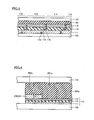
- Fig. 1 is an exploded perspective view of a portion in configuration of a solar cell module having a laminated glass structure according to one embodiment of the present invention.
- Fig. 2 is a partial cross section of a solar cell shown in Fig. 1 , as taken and seen along an arrow II-II shown in Fig 1 .
- a first glass substrate or a glass substrate 100 bears a plurality of elongate solar cells 110 thereon in parallel.
- solar cell 110 includes glass substrate 100 located at a front surface (or a light receiving surface), a transparent electrode layer (an electrode layer adjacent to the front surface) 111 provided behind glass substrate 100, a photoelectric conversion layer 113 provided behind transparent electrode layer 111, and a back surface electrode layer 115 provided behind photoelectric conversion layer 113.
- Transparent electrode layer 111, photoelectric conversion layer 113, and back surface electrode layer 115 are each patterned as prescribed.
- Transparent electrode layer 111, photoelectric conversion layer 113, and back surface electrode layer 115 are provided with a first separation line 112, a second separation line 114, and a third separation line 116,respectively, extending along solar cell 110.
- First separation line 112 provided in transparent electrode layer 111 has photoelectric conversion layer 113 introduced therein.
- Second separation line 114 provided in photoelectric conversion layer 113 has back surface electrode layer 115 introduced therein.
- Individual photoelectric conversion layers 113 divided by second separation line 114 are sandwiched between individual transparent electrode layers 111 divided by first separation line 112 and individual back surface electrode layers 115 divided by third separation line 116.
- Back surface electrode layer 115 that is opposite to one transparent electrode layer 111 is connected to another transparent electrode layer 111 adjacent to the one transparent electrode layer 111 via a portion of back surface electrode layer 115 that is introduced in second separation line 114 dividing photoelectric conversion layer 113. Note that the portion of back surface electrode layer 115 is referred to as a contact line, in particular.
- Solar cell 110 is fabricated in a method, as will be described hereinafter.
- Thermal chemical vapor deposition (CVD) or the like is employed to deposit transparent electrode layer 111 on glass substrate 100.
- Transparent electrode layer 111 can for example be tin oxide (SnO 2 ) film, zinc oxide (ZnO) film, indium tin oxide (ITO) film, or the like.
- transparent electrode layer 111 is laser-scribed or the like and thus partially removed to form a plurality of first separation lines 112. This divides transparent electrode layer 111 into a plurality thereof. This can be done by using laser light that is a fundamental wave of yttrium aluminum garnet (YAG) laser (wavelength: 1064 nm) or the like for example.
- YAG yttrium aluminum garnet
- Photoelectric conversion layer 113 can be thin semiconductor film, and can for example be p, i and n layers formed of thin amorphous silicon film and successively stacked, one on another. This deposition allows first separation line 112 to have photoelectric conversion layer 113 introduced therein.
- photoelectric conversion layer 113 is laser-scribed or the like and thus partially removed to form a plurality of second separation lines 114.
- Back surface electrode layers 115 can for example be zinc oxide (ZnO) film/silver (Ag) film, ZnO film/aluminum (Al) film, ITO film/Ag film, SnO 2 film/Ag film, or similar films stacked in layers.
- ZnO zinc oxide
- Si silver
- Al zinc oxide
- ITO film/Ag film ITO film/Ag film
- SnO 2 film/Ag film or similar films stacked in layers.
- back surface electrode layer 115 is laser-scribed or the like and thus partially removed to form a plurality of third separation lines 116. This divides back surface electrode layer 115 into a plurality thereof. This can be done by using laser light that is second harmonic of YAG laser (wavelength: 532 nm) or the like for example.
- Solar cell string 120 thus formed has opposite ends, i.e., solar cell 110 located at an end portion in a direction in which the plurality of solar cells 110 are aligned, to serve as a region to extract electric power from solar cell string 120.
- bus bar 130 is an elongate plate of metallic foil.
- Bus bar 130 has a generally center portion, as seen along bus bar 130, connected to a lead wire 140 at one end thereof serving as a connection portion 141.
- Lead wire 140 extends in a direction transverse to bus bar 130.
- Lead wire 140 is an elongate plate of metallic foil.
- Lead wire 140 has the other end provided with a terminal portion 142 bent to be orthogonal to a direction in which lead wire 140 extends.
- Lead wire 140 at a side thereof excluding its opposite ends and facing solar cell 110 is covered with an insulating film 150.
- Bus bar 130 and lead wire 140 configure a leader line for extracting electric power generated by the plurality of solar cells 110.
- Bus bar 130 and lead wire 140 are previously connected together via solder or the like before bus bar 130 is connected to solar cell 110.
- solar cell string 120 When solar cell string 120 has one end to serve as a positive side, it has the other end to serve as a negative side. As such, bus bar 130 and lead wire 140 are disposed at the positive and negative sides and thus configure a pair of leader lines.
- Fig. 3 is a perspective view of the solar cell with the leader line thereon.
- Fig. 4 is an exploded perspective view in configuration of the solar cell module having the laminated glass structure according to the present embodiment.
- Fig. 5 is a partial cross section of the solar cell module having the laminated glass structure according to the present embodiment, as seen in the same direction as Fig. 2 .
- bus bar 130 is connected to back surface electrode layer 115 via a conductive paste previously applied to back surface electrode layer 115.
- solar cell string 120 has the positive and negative sides led to terminal portion 142 of the pair of leader lines.
- the solar cell module having the laminated glass structure includes a second glass substrate or glass substrate 170 cooperating with glass substrate 100 to sandwich the plurality of solar cells 110 and a portion of the leader line other than terminal portion 142.
- Glass substrate 170 has an opening 170h allowing the leader line to have terminal portion 142 passing therethrough.
- the solar cell module having the laminated glass structure includes a resin sealant 160 sealing the plurality of solar cells 110 and the portion of the leader line other than terminal portion 142 between glass substrate 100 and glass substrate 170.
- Resin sealant 160 has an opening 160h allowing the leader line to have terminal portion 142 passing therethrough.
- Resin sealant 160 can for example be polyethylene terephthalate (PET) resin, ethylene vinyl acetate copolymer resin (EVA), ionomer resin, or the like.
- a vacuum lamination device is used to sandwich glass substrates 100 and 170 and thus externally apply pressure thereto and therewhile heat the intermediate product to fuse resin sealant 160, and thereafter it is set. Note that it is heated to 100-200 degrees centigrade.
- the solar cell module having the laminated glass structure is thus produced.
- the solar cell module having the laminated glass structure thus produced has back surface electrode layer 115 covered with resin sealant 160 provided therebehind, as shown in Fig. 5 .
- Third separation line 116 formed in back surface electrode layer 115 has resin sealant 160 introduced therein.
- Resin sealant 160 is covered with glass substrate 170 provided therebehind.
- the leader line has terminal portion 142 extracted outside resin sealant 160 and glass substrate 170, and a terminal box (not shown) is attached to terminal portion 142 behind glass substrate 170.
- solar cell 110 may have transparent electrode layer 111 and photoelectric conversion layer 113 peeled off from each other or photoelectric conversion layer 113 and back surface electrode layer 115 peeled off from each other.
- solar cell 110 may have transparent electrode layer 111 and photoelectric conversion layer 113 peeled off from each other or photoelectric conversion layer 113 and back surface electrode layer 115 peeled off from each other, and a method for solving the same.
- Fig. 6 dimensionally shows in cross section as a comparative example 1 a solar cell module having a laminated glass structure that is not of thin profile with a resin sealant heated to 125 degrees centigrade and thus fused. Note that Fig. 6 does not show first separation line 112, second separation line 114, or third separation line 116 for simplicity.
- a vacuum lamination device is employed to heat the resin sealant to 125 degrees centigrade and thus fuse the resin sealant, which is shown in the figure as resin sealant 260a, and resin sealant 260a has a portion between the plurality of solar cells 110 and glass substrate 170 which is shown in the figure as resin sealant 261a having a thickness L 1 for the sake of illustration.
- the leader line has a portion, i.e., bus bar 230 and the lead wire's connection portion 241, having a thickness d 1 for the sake of illustration.
- the resin sealant heated by the vacuum lamination device to 125 degrees centigrade and thus fused, or resin sealant 260a will have a portion between the leader line and glass substrate 170 which is shown in the figure as resin sealant 262a having a thickness L 1 - d 1 .
- Resin sealant 260a fused is thermally set at 100-200 degrees centigrade.
- Fig. 7 dimensionally shows in cross section comparative example 1 with the resin sealant thermally set and subsequently cooled to 25 degrees centigrade and having shrunk freely.
- the resin sealant has a coefficient of linear expansion represented as ⁇ x 10 -2 /K for the sake of illustration.
- resin sealant 261b located between the plurality of solar cells 110 and glass substrate 170 will shrink in thickness in an amount L 1 x ⁇ .
- resin sealant 262b located between the leader line and glass substrate 170 will shrink in thickness in an amount (L 1 - d 1 ) x ⁇ .
- resin sealant 261b and resin sealant 262b shrink in thickness in amounts, respectively, with a difference of d 1 x ⁇ . That is, the resin sealant shrinks in thickness in amounts with a difference in proportion to the leader line's thickness.
- Fig. 8 dimensionally shows in cross section comparative example 1 with the resin sealant thermally set and subsequently cooled to 25 degrees centigrade and having shrunk.
- resin sealant 260 that has been thermally set has been bonded to glass substrate 170 and accordingly, it cannot shrink freely when it is cooled to 25 degrees centigrade.
- resin sealant 261 that is located between the plurality of solar cells 110 and glass substrate 170 and shrinks in a large amount can, in reality, only shrink in thickness to that of resin sealant 262 that is located between the leader line and glass substrate 170 and shrinks in a small amount.
- Fig. 9 dimensionally shows in cross section as comparative example 2 a solar cell module having a laminated glass structure with the resin sealant reduced in thickness, and heated to 125 degrees centigrade and thus fused. Note that Fig. 9 does not show first separation line 112, second separation line 114, or third separation line 116 for simplicity.
- the vacuum lamination device is employed to heat the resin sealant to 125 degrees centigrade and thus fuse the resin sealant, which is shown in the figure as resin sealant 160a, and resin sealant 160a has a portion between the plurality of solar cells 110 and glass substrate 170 which is shown in the figure as resin sealant 161a having a thickness L 2 for the sake of illustration.
- L 1 > L 2 .
- the leader line has a portion, i.e., bus bar 230 and the lead wire's connection portion 241, having thickness d 1 for the sake of illustration.
- the resin sealant heated by the vacuum lamination device to 125 degrees centigrade and thus fused, or resin sealant 160a will have a portion between the leader line and glass substrate 170 which is shown in the figure as resin sealant 162a having a thickness L 2 - d 1 .
- Fig. 10 dimensionally shows in cross section comparative example 2 with the resin sealant thermally set and subsequently cooled to 25 degrees centigrade and having shrunk freely.
- resin sealant 161b located between the plurality of solar cells 110 and glass substrate 170 will shrink in thickness in an amount L 2 x ⁇ .
- resin sealant 162b located between the leader line and glass substrate 170 will shrink in thickness in an amount (L 2 - d 1 ) x ⁇ .
- resin sealant 161b and resin sealant 162b shrink in thickness in amounts, respectively, with a difference d 1 x ⁇ . That is, comparative example 2 also has the resin sealant shrinking in thickness in amounts with a difference in proportion to the leader line's thickness. Comparative example 2 has resin sealant 160 smaller in thickness than comparative example 1, and accordingly, a ratio of a difference between amounts by which the resin sealant shrinks to the resin sealant's thickness is larger in comparative example 2 than in comparative example 1.
- Fig. 11 dimensionally shows in cross section comparative example 2 with the resin sealant thermally set and subsequently cooled to 25 degrees centigrade and having shrunk.
- resin sealant 160 that has been thermally set has been bonded to glass substrate 170 and accordingly, it cannot shrink freely when it is cooled to 25 degrees centigrade.
- resin sealant 161 that is located between the plurality of solar cells 110 and glass substrate 170 and shrinks in a large amount can, in reality, only shrink in thickness to that of resin sealant 162 that is located between the leader line and glass substrate 170 and shrinks in a small amount.
- comparative example 2 has a larger ratio of a difference between amounts by which the resin sealant shrinks to the resin sealant's thickness than comparative example 1, and accordingly, comparative example 2 has resin sealant 161 experiencing larger internal stress than comparative example 1.
- comparative example 2 has glass substrate 170 and solar cell 110 experiencing larger depthwise tensile stress than comparative example 1.
- solar cell 110 may have transparent electrode layer 111 and photoelectric conversion layer 113 peeled off from each other or back surface electrode layer 115 and photoelectric conversion layer 113 peeled off from each other.
- the leader line is reduced in thickness to correspond to the resin sealant in thickness to alleviate internal stress caused in the resin sealant.
- Fig. 12 dimensionally shows in cross section the present embodiment that is a solar cell module having a laminated glass structure with a resin sealant reduced in thickness, and heated to 125 degrees centigrade and thus fused. Note that Fig. 12 does not show first separation line 112, second separation line 114, or third separation line 116 for simplicity.
- the vacuum lamination device is employed to heat the resin sealant to 125 degrees centigrade and thus fuse the resin sealant, which is shown in the figure as resin sealant 160a, and resin sealant 160a has a portion between the plurality of solar cells 110 and glass substrate 170 which is shown in the figure as resin sealant 161a having thickness L 2 for the sake of illustration.
- L 2 is 1.5 mm or smaller, for example.
- the leader line has a portion, i.e., bus bar 130 and the lead wire 140 connection portion 141, having a thickness d 2 for the sake of illustration. Note that d 1 > d 2 .
- the resin sealant heated by the vacuum lamination device to 125 degrees centigrade and thus fused, or resin sealant 160a will have a portion between the leader line and glass substrate 170 which is shown in the figure as resin sealant 162a having a thickness L 2 - d 2 .
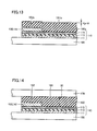
- Fig. 13 dimensionally shows in cross section the present embodiment with the resin sealant thermally set and subsequently cooled to 25 degrees centigrade and having shrunk freely.
- resin sealant 161b located between the plurality of solar cells 110 and glass substrate 170 will shrink in thickness in an amount L 2 x ⁇ .
- resin sealant 162b located between the leader line and glass substrate 170 will shrink in thickness in an amount (L 2 - d 2 ) x ⁇ .
- resin sealant 161b and resin sealant 162b shrink in thickness in amounts, respectively, with a difference d 2 x ⁇ . That is, the present embodiment also has the resin sealant shrinking in thickness in amounts with a difference in proportion to the leader line's thickness.
- the present embodiment has a leader line smaller in thickness than comparative example 2, and accordingly, the present embodiment has the resin sealant shrinking in thickness in amounts with a difference smaller than comparative example 2 does.
- Fig. 14 dimensionally shows in cross section the present embodiment with the resin sealant thermally set and subsequently cooled to 25 degrees centigrade and having shrunk.
- resin sealant 160 that has been thermally set has been bonded to glass substrate 170 and accordingly, it cannot shrink freely when it is cooled to 25 degrees centigrade.
- resin sealant 161 that is located between the plurality of solar cells 110 and glass substrate 170 and shrinks in a large amount can, in reality, only shrink in thickness to that of resin sealant 162 that is located between the leader line and glass substrate 170 and shrinks in a small amount.
- the present embodiment has the resin sealant shrinking in thickness in amounts with a difference smaller than comparative example 2, and accordingly, the present embodiment has resin sealant 161 experiencing smaller internal stress than comparative example 2.
- the present embodiment has glass substrate 170 and solar cell 110 experiencing smaller depthwise tensile stress than comparative example 2.
- the leader line reduced in thickness to correspond to the resin sealant in thickness can contribute to alleviated internal stress caused in the resin sealant. This can minimize film peeling off in solar cell 110 in a solar cell module having a laminated glass structure of thin profile.
- Resin sealant 160 of HIMILAN ® containing ionomer resin was used to fabricate a solar cell module having a laminated glass structure similar in configuration to the solar cell module having the laminated glass structure according to the present embodiment.
- Resin sealant 160 reduced in thickness to 400 ⁇ m or smaller allows the solar cell module to have an end face allowing resin sealant 160 to have only a limited area externally exposed and can thus minimize external moisture or the like entering the solar cell module and hence enhance the solar cell module in weatherability.
- Resin sealant 160 heated by the vacuum lamination device to 125 degrees centigrade and thus fused has a portion between the plurality of solar cells 110 and glass substrate 170, i.e., resin sealant 161, having a thickness L 3 for the sake of illustration. Furthermore, between glass substrate 100 and glass substrate 170 the leader line has a portion, i.e., bus bar 130 and the lead wire 140 connection portion 141, having a thickness d 3 for the sake of illustration.
- the solar cell module having the laminated glass structure of thin profile having a plurality of solar cells 110 and glass substrate 170 with resin sealant 161 of 400 ⁇ m or smaller in thickness therebetween, with a leader line having a portion (i.e., bus bar 130 and the lead wire 140 connection portion 141) set in thickness to 30% or smaller relative to that of resin sealant 161 located between the plurality of solar cells 110 and glass substrate 170, can alleviate internal stress caused in resin sealant 161 and minimize film peeling off in solar cell 110.
- a solar cell module having a laminated glass structure that has a thin profile and can also minimize an increasing defect rate, and is significantly transparent, can be constantly produced.
- the leader line preferably has a portion (i.e., bus bar 130 and the lead wire 140 connection portion 141) set in thickness to 17% or larger relative to that of resin sealant 161 located between the plurality of solar cells 110 and glass substrate 170.
Landscapes
- Photovoltaic Devices (AREA)
Abstract
Description
- The present invention relates to a solar cell module having a laminated glass structure.
- A solar cell module having a laminated glass structure is configured as disclosed in a prior art document, Japanese Patent Laying-Open No.
2008-258269 - PTD 1: Japanese Patent Laying-Open No.
2008-258269 - There is a demand that the solar cell module having the laminated glass structure as described in PTD 1 and the like be formed of a smaller number of members and have a thin profile for reduced cost.
- The present invention has been made to address the above issue and contemplates a solar cell module having a laminated glass structure that is inexpensive and has a thin profile.
- The present invention provides a solar cell module having a laminated glass structure, including: a first glass substrate; a plurality of solar cells provided on the first glass substrate and electrically interconnected; and a leader line provided on the plurality of solar cells for extracting electric power generated by the plurality of solar cells. Furthermore, the solar cell module having the laminated glass structure includes: a second glass substrate opposite to the first glass substrate with the plurality of solar cells and a portion of the leader line posed therebetween; and a resin sealant sealing the plurality of solar cells and the portion of the leader line located between the first glass substrate and the second glass substrate. The leader line has the portion set in thickness to at most 30% relative to that of the resin sealant located between the plurality of solar cells and the second glass substrate.
- Preferably, the resin sealant located between the plurality of solar cells and the second glass substrate is at most 400 µm in thickness.
- In one embodiment of the present invention, the resin sealant is thermally set at 100-200 degrees centigrade.
- In one embodiment of the present invention, the resin sealant includes ionomer resin.
- The present invention can thus provide a solar cell module having a laminated glass structure that is reduced in thickness.
-
-
Fig. 1 is an exploded perspective view of a portion in configuration of a solar cell module having a laminated glass structure according to an embodiment of the present invention. -
Fig. 2 is a partial cross section of a solar cell shown inFig. 1 , as taken and seen along an arrow II-II shown inFig 1 . -
Fig. 3 is a perspective view of the solar cell with a leader line thereon. -
Fig. 4 is an exploded perspective view in configuration of the solar cell module having the laminated glass structure according to the present embodiment. -
Fig. 5 is a cross section of the solar cell module having the laminated glass structure according to the present embodiment, as seen in the same direction asFig. 2 . -
Fig. 6 dimensionally shows in cross section as a comparative example 1 a solar cell module having a laminated glass structure that is not of thin profile with a resin sealant heated to 125 degrees centigrade and thus fused. -
Fig. 7 dimensionally shows in cross section comparative example 1 with the resin sealant thermally set and subsequently cooled to 25 degrees centigrade and having shrunk freely. -
Fig. 8 dimensionally shows in cross section comparative example 1 with the resin sealant thermally set and subsequently cooled to 25 degrees centigrade and having shrunk. -
Fig. 9 dimensionally shows in cross section as a comparative example 2 a solar cell module having a laminated glass structure with a resin sealant reduced in thickness, and heated to 125 degrees centigrade and thus fused. -
Fig. 10 dimensionally shows in cross section comparative example 2 with the resin sealant thermally set and subsequently cooled to 25 degrees centigrade and having shrunk freely. -
Fig. 11 dimensionally shows in cross section comparative example 2 with the resin sealant thermally set and subsequently cooled to 25 degrees centigrade and having shrunk. -
Fig. 12 dimensionally shows in cross section the present embodiment that is a solar cell module having a laminated glass structure with a resin sealant reduced in thickness, and heated to 125 degrees centigrade and thus fused. -
Fig. 13 dimensionally shows in cross section the present embodiment with the resin sealant thermally set and subsequently cooled to 25 degrees centigrade and having shrunk freely. -
Fig. 14 dimensionally shows in cross section the present embodiment with the resin sealant thermally set and subsequently cooled to 25 degrees centigrade and having shrunk. - The present invention in one embodiment provides a solar cell module having a laminated glass structure, as will be described hereinafter. In describing the following embodiment(s), components identically or correspondingly shown in the figures are identically denoted and will not be described repeatedly.
-
Fig. 1 is an exploded perspective view of a portion in configuration of a solar cell module having a laminated glass structure according to one embodiment of the present invention.Fig. 2 is a partial cross section of a solar cell shown inFig. 1 , as taken and seen along an arrow II-II shown inFig 1 . - As shown in
Fig. 1 , a first glass substrate or aglass substrate 100 bears a plurality of elongatesolar cells 110 thereon in parallel. - As shown in
Fig. 2 ,solar cell 110 includesglass substrate 100 located at a front surface (or a light receiving surface), a transparent electrode layer (an electrode layer adjacent to the front surface) 111 provided behindglass substrate 100, aphotoelectric conversion layer 113 provided behindtransparent electrode layer 111, and a backsurface electrode layer 115 provided behindphotoelectric conversion layer 113. -
Transparent electrode layer 111,photoelectric conversion layer 113, and backsurface electrode layer 115 are each patterned as prescribed.Transparent electrode layer 111,photoelectric conversion layer 113, and backsurface electrode layer 115 are provided with afirst separation line 112, asecond separation line 114, and athird separation line 116,respectively, extending alongsolar cell 110. -
First separation line 112 provided intransparent electrode layer 111 hasphotoelectric conversion layer 113 introduced therein.Second separation line 114 provided inphotoelectric conversion layer 113 has backsurface electrode layer 115 introduced therein. - Individual
photoelectric conversion layers 113 divided bysecond separation line 114 are sandwiched between individualtransparent electrode layers 111 divided byfirst separation line 112 and individual backsurface electrode layers 115 divided bythird separation line 116. - Back
surface electrode layer 115 that is opposite to onetransparent electrode layer 111 is connected to anothertransparent electrode layer 111 adjacent to the onetransparent electrode layer 111 via a portion of backsurface electrode layer 115 that is introduced insecond separation line 114 dividingphotoelectric conversion layer 113. Note that the portion of backsurface electrode layer 115 is referred to as a contact line, in particular. - This allows individual
photoelectric conversion layers 113 to be electrically interconnected via backsurface electrode layer 115 andtransparent electrode layer 111 and thus connects a plurality ofsolar cells 110 that are included in asolar cell string 120 in series. -
Solar cell 110 is fabricated in a method, as will be described hereinafter. Thermal chemical vapor deposition (CVD) or the like is employed to deposittransparent electrode layer 111 onglass substrate 100.Transparent electrode layer 111 can for example be tin oxide (SnO2) film, zinc oxide (ZnO) film, indium tin oxide (ITO) film, or the like. - Then,
transparent electrode layer 111 is laser-scribed or the like and thus partially removed to form a plurality offirst separation lines 112. This dividestransparent electrode layer 111 into a plurality thereof. This can be done by using laser light that is a fundamental wave of yttrium aluminum garnet (YAG) laser (wavelength: 1064 nm) or the like for example. - Subsequently, plasma CVD or the like is employed to deposit
photoelectric conversion layer 113 ontransparent electrode layer 111.Photoelectric conversion layer 113 can be thin semiconductor film, and can for example be p, i and n layers formed of thin amorphous silicon film and successively stacked, one on another. This deposition allowsfirst separation line 112 to havephotoelectric conversion layer 113 introduced therein. - Then,
photoelectric conversion layer 113 is laser-scribed or the like and thus partially removed to form a plurality ofsecond separation lines 114. This dividesphotoelectric conversion layer 113 into a plurality thereof. This can be done by using laser light that is second harmonic of YAG laser (wavelength: 532 nm) or the like for example. - Subsequently, magnetron sputtering, electron-beam vapor deposition or the like is employed to deposit back
surface electrode layer 115 onphotoelectric conversion layer 113. Backsurface electrode layers 115 can for example be zinc oxide (ZnO) film/silver (Ag) film, ZnO film/aluminum (Al) film, ITO film/Ag film, SnO2 film/Ag film, or similar films stacked in layers. This deposition allowssecond separation line 114 to have backsurface electrode layer 115 introduced therein and thus forms the contact line as described above. - Then, back
surface electrode layer 115 is laser-scribed or the like and thus partially removed to form a plurality ofthird separation lines 116. This divides backsurface electrode layer 115 into a plurality thereof. This can be done by using laser light that is second harmonic of YAG laser (wavelength: 532 nm) or the like for example. -
Solar cell string 120 thus formed has opposite ends, i.e.,solar cell 110 located at an end portion in a direction in which the plurality ofsolar cells 110 are aligned, to serve as a region to extract electric power fromsolar cell string 120. - Hereinafter, a leader line will be described that extracts generated electric power from the plurality of
solar cells 110. As shown inFig. 1 ,solar cell string 120 has the opposite ends with theirsolar cells 110 opposite tobus bars 130, respectively.Bus bar 130 is an elongate plate of metallic foil.Bus bar 130 has a generally center portion, as seen alongbus bar 130, connected to alead wire 140 at one end thereof serving as aconnection portion 141. -
Lead wire 140 extends in a direction transverse tobus bar 130.Lead wire 140 is an elongate plate of metallic foil.Lead wire 140 has the other end provided with aterminal portion 142 bent to be orthogonal to a direction in which leadwire 140 extends.Lead wire 140 at a side thereof excluding its opposite ends and facingsolar cell 110 is covered with an insulatingfilm 150. -
Bus bar 130 andlead wire 140 configure a leader line for extracting electric power generated by the plurality ofsolar cells 110.Bus bar 130 andlead wire 140 are previously connected together via solder or the like beforebus bar 130 is connected tosolar cell 110. - When
solar cell string 120 has one end to serve as a positive side, it has the other end to serve as a negative side. As such,bus bar 130 andlead wire 140 are disposed at the positive and negative sides and thus configure a pair of leader lines. -
Fig. 3 is a perspective view of the solar cell with the leader line thereon.Fig. 4 is an exploded perspective view in configuration of the solar cell module having the laminated glass structure according to the present embodiment.Fig. 5 is a partial cross section of the solar cell module having the laminated glass structure according to the present embodiment, as seen in the same direction asFig. 2 . - As shown in
Fig. 3 ,bus bar 130 is connected to backsurface electrode layer 115 via a conductive paste previously applied to backsurface electrode layer 115. As a result,solar cell string 120 has the positive and negative sides led toterminal portion 142 of the pair of leader lines. - As shown in
Fig. 4 , the solar cell module having the laminated glass structure includes a second glass substrate orglass substrate 170 cooperating withglass substrate 100 to sandwich the plurality ofsolar cells 110 and a portion of the leader line other thanterminal portion 142.Glass substrate 170 has anopening 170h allowing the leader line to haveterminal portion 142 passing therethrough. - Furthermore, the solar cell module having the laminated glass structure includes a
resin sealant 160 sealing the plurality ofsolar cells 110 and the portion of the leader line other thanterminal portion 142 betweenglass substrate 100 andglass substrate 170.Resin sealant 160 has anopening 160h allowing the leader line to haveterminal portion 142 passing therethrough.Resin sealant 160 can for example be polyethylene terephthalate (PET) resin, ethylene vinyl acetate copolymer resin (EVA), ionomer resin, or the like. - After
resin sealant 160 andglass substrate 170 are disposed, a vacuum lamination device is used tosandwich glass substrates resin sealant 160, and thereafter it is set. Note that it is heated to 100-200 degrees centigrade. The solar cell module having the laminated glass structure is thus produced. - The solar cell module having the laminated glass structure thus produced has back
surface electrode layer 115 covered withresin sealant 160 provided therebehind, as shown inFig. 5 .Third separation line 116 formed in backsurface electrode layer 115 hasresin sealant 160 introduced therein.Resin sealant 160 is covered withglass substrate 170 provided therebehind. - The leader line has
terminal portion 142 extracted outsideresin sealant 160 andglass substrate 170, and a terminal box (not shown) is attached toterminal portion 142 behindglass substrate 170. - The present inventors have found that when the solar cell module having the laminated glass structure produced as described above is reduced in thickness there is a possibility that
solar cell 110 may havetransparent electrode layer 111 andphotoelectric conversion layer 113 peeled off from each other orphotoelectric conversion layer 113 and backsurface electrode layer 115 peeled off from each other. - Hereinafter will be described how
solar cell 110 may havetransparent electrode layer 111 andphotoelectric conversion layer 113 peeled off from each other orphotoelectric conversion layer 113 and backsurface electrode layer 115 peeled off from each other, and a method for solving the same. -
Fig. 6 dimensionally shows in cross section as a comparative example 1 a solar cell module having a laminated glass structure that is not of thin profile with a resin sealant heated to 125 degrees centigrade and thus fused. Note thatFig. 6 does not showfirst separation line 112,second separation line 114, orthird separation line 116 for simplicity. - As shown in
Fig. 6 , in comparative example 1, a vacuum lamination device is employed to heat the resin sealant to 125 degrees centigrade and thus fuse the resin sealant, which is shown in the figure asresin sealant 260a, andresin sealant 260a has a portion between the plurality ofsolar cells 110 andglass substrate 170 which is shown in the figure asresin sealant 261a having a thickness L1 for the sake of illustration. Furthermore, in comparative example 1, betweenglass substrate 100 andglass substrate 170 the leader line has a portion, i.e., bus bar 230 and the lead wire's connection portion 241, having a thickness d1 for the sake of illustration. - Accordingly, in comparative example 1, the resin sealant heated by the vacuum lamination device to 125 degrees centigrade and thus fused, or
resin sealant 260a, will have a portion between the leader line andglass substrate 170 which is shown in the figure asresin sealant 262a having a thickness L1 - d1. -
Resin sealant 260a fused is thermally set at 100-200 degrees centigrade.Fig. 7 dimensionally shows in cross section comparative example 1 with the resin sealant thermally set and subsequently cooled to 25 degrees centigrade and having shrunk freely. Herein, the resin sealant has a coefficient of linear expansion represented as α x 10-2/K for the sake of illustration. - When
glass substrate 170 is not disposed, and the product is cooled by 100 degrees centigrade andresin sealant 260b thermally set shrinks,resin sealant 261b located between the plurality ofsolar cells 110 andglass substrate 170 will shrink in thickness in an amount L1 x α. In contrast,resin sealant 262b located between the leader line andglass substrate 170 will shrink in thickness in an amount (L1 - d1) x α. - As shown in
Fig. 7 ,resin sealant 261b andresin sealant 262b shrink in thickness in amounts, respectively, with a difference of d1 x α. That is, the resin sealant shrinks in thickness in amounts with a difference in proportion to the leader line's thickness. -
Fig. 8 dimensionally shows in cross section comparative example 1 with the resin sealant thermally set and subsequently cooled to 25 degrees centigrade and having shrunk. As shown inFig. 8 ,resin sealant 260 that has been thermally set has been bonded toglass substrate 170 and accordingly, it cannot shrink freely when it is cooled to 25 degrees centigrade. - In other words,
resin sealant 261 that is located between the plurality ofsolar cells 110 andglass substrate 170 and shrinks in a large amount can, in reality, only shrink in thickness to that ofresin sealant 262 that is located between the leader line andglass substrate 170 and shrinks in a small amount. - This causes internal stress in
resin sealant 261. By this internal stress, as indicated inFig. 8 by anarrow 10,glass substrate 170 andsolar cell 110 experience depthwise tensile stress. - Hereinafter will be described a solar cell module having a laminated glass structure of a comparative example 2 having the resin sealant reduced in thickness for thin profile.
-
Fig. 9 dimensionally shows in cross section as comparative example 2 a solar cell module having a laminated glass structure with the resin sealant reduced in thickness, and heated to 125 degrees centigrade and thus fused. Note thatFig. 9 does not showfirst separation line 112,second separation line 114, orthird separation line 116 for simplicity. - As shown in
Fig. 9 , in comparative example 2, the vacuum lamination device is employed to heat the resin sealant to 125 degrees centigrade and thus fuse the resin sealant, which is shown in the figure asresin sealant 160a, andresin sealant 160a has a portion between the plurality ofsolar cells 110 andglass substrate 170 which is shown in the figure asresin sealant 161a having a thickness L2 for the sake of illustration. Note that L1 > L2. Furthermore, in comparative example 2, betweenglass substrate 100 andglass substrate 170 the leader line has a portion, i.e., bus bar 230 and the lead wire's connection portion 241, having thickness d1 for the sake of illustration. - Accordingly, in comparative example 2, the resin sealant heated by the vacuum lamination device to 125 degrees centigrade and thus fused, or
resin sealant 160a, will have a portion between the leader line andglass substrate 170 which is shown in the figure asresin sealant 162a having a thickness L2 - d1. -
Fig. 10 dimensionally shows in cross section comparative example 2 with the resin sealant thermally set and subsequently cooled to 25 degrees centigrade and having shrunk freely. - When
glass substrate 170 is not disposed, and the product is cooled by 100 degrees centigrade andresin sealant 160b thermally set shrinks,resin sealant 161b located between the plurality ofsolar cells 110 andglass substrate 170 will shrink in thickness in an amount L2 x α. In contrast,resin sealant 162b located between the leader line andglass substrate 170 will shrink in thickness in an amount (L2 - d1) x α. - As shown in
Fig. 10 ,resin sealant 161b andresin sealant 162b shrink in thickness in amounts, respectively, with a difference d1 x α. That is, comparative example 2 also has the resin sealant shrinking in thickness in amounts with a difference in proportion to the leader line's thickness. Comparative example 2 hasresin sealant 160 smaller in thickness than comparative example 1, and accordingly, a ratio of a difference between amounts by which the resin sealant shrinks to the resin sealant's thickness is larger in comparative example 2 than in comparative example 1. -
Fig. 11 dimensionally shows in cross section comparative example 2 with the resin sealant thermally set and subsequently cooled to 25 degrees centigrade and having shrunk. As shown inFig. 11 ,resin sealant 160 that has been thermally set has been bonded toglass substrate 170 and accordingly, it cannot shrink freely when it is cooled to 25 degrees centigrade. - In other words,
resin sealant 161 that is located between the plurality ofsolar cells 110 andglass substrate 170 and shrinks in a large amount can, in reality, only shrink in thickness to that ofresin sealant 162 that is located between the leader line andglass substrate 170 and shrinks in a small amount. - As has been set forth above, comparative example 2 has a larger ratio of a difference between amounts by which the resin sealant shrinks to the resin sealant's thickness than comparative example 1, and accordingly, comparative example 2 has
resin sealant 161 experiencing larger internal stress than comparative example 1. By this internal stress, as indicated inFig. 11 by anarrow 20, comparative example 2 hasglass substrate 170 andsolar cell 110 experiencing larger depthwise tensile stress than comparative example 1. - In that case,
solar cell 110 may havetransparent electrode layer 111 andphotoelectric conversion layer 113 peeled off from each other or backsurface electrode layer 115 andphotoelectric conversion layer 113 peeled off from each other. - Accordingly, in the present embodiment, the leader line is reduced in thickness to correspond to the resin sealant in thickness to alleviate internal stress caused in the resin sealant.
Fig. 12 dimensionally shows in cross section the present embodiment that is a solar cell module having a laminated glass structure with a resin sealant reduced in thickness, and heated to 125 degrees centigrade and thus fused. Note thatFig. 12 does not showfirst separation line 112,second separation line 114, orthird separation line 116 for simplicity. - As shown in
Fig. 12 , in the present embodiment, the vacuum lamination device is employed to heat the resin sealant to 125 degrees centigrade and thus fuse the resin sealant, which is shown in the figure asresin sealant 160a, andresin sealant 160a has a portion between the plurality ofsolar cells 110 andglass substrate 170 which is shown in the figure asresin sealant 161a having thickness L2 for the sake of illustration. L2 is 1.5 mm or smaller, for example. Furthermore, in the present embodiment, betweenglass substrate 100 andglass substrate 170 the leader line has a portion, i.e.,bus bar 130 and thelead wire 140connection portion 141, having a thickness d2 for the sake of illustration. Note that d1 > d2. - Accordingly, in the present embodiment, the resin sealant heated by the vacuum lamination device to 125 degrees centigrade and thus fused, or
resin sealant 160a, will have a portion between the leader line andglass substrate 170 which is shown in the figure asresin sealant 162a having a thickness L2 - d2. -
Fig. 13 dimensionally shows in cross section the present embodiment with the resin sealant thermally set and subsequently cooled to 25 degrees centigrade and having shrunk freely. - When
glass substrate 170 is not disposed, and the product is cooled by 100 degrees centigrade andresin sealant 160b thermally set shrinks,resin sealant 161b located between the plurality ofsolar cells 110 andglass substrate 170 will shrink in thickness in an amount L2 x α. In contrast,resin sealant 162b located between the leader line andglass substrate 170 will shrink in thickness in an amount (L2 - d2) x α. - As shown in
Fig. 13 ,resin sealant 161b andresin sealant 162b shrink in thickness in amounts, respectively, with a difference d2 x α. That is, the present embodiment also has the resin sealant shrinking in thickness in amounts with a difference in proportion to the leader line's thickness. The present embodiment has a leader line smaller in thickness than comparative example 2, and accordingly, the present embodiment has the resin sealant shrinking in thickness in amounts with a difference smaller than comparative example 2 does. -
Fig. 14 dimensionally shows in cross section the present embodiment with the resin sealant thermally set and subsequently cooled to 25 degrees centigrade and having shrunk. As shown inFig. 14 ,resin sealant 160 that has been thermally set has been bonded toglass substrate 170 and accordingly, it cannot shrink freely when it is cooled to 25 degrees centigrade. - In other words,
resin sealant 161 that is located between the plurality ofsolar cells 110 andglass substrate 170 and shrinks in a large amount can, in reality, only shrink in thickness to that ofresin sealant 162 that is located between the leader line andglass substrate 170 and shrinks in a small amount. - As has been set forth above, the present embodiment has the resin sealant shrinking in thickness in amounts with a difference smaller than comparative example 2, and accordingly, the present embodiment has
resin sealant 161 experiencing smaller internal stress than comparative example 2. By this internal stress, as indicated inFig. 14 by anarrow 30, the present embodiment hasglass substrate 170 andsolar cell 110 experiencing smaller depthwise tensile stress than comparative example 2. - Thus the leader line reduced in thickness to correspond to the resin sealant in thickness can contribute to alleviated internal stress caused in the resin sealant. This can minimize film peeling off in
solar cell 110 in a solar cell module having a laminated glass structure of thin profile. - Hereinafter will be described an exemplary experiment conducted with the resin sealant and the leader line varied in thickness to examine whether
solar cell 110 has peeling off therein. -
Resin sealant 160 of HIMILAN® containing ionomer resin was used to fabricate a solar cell module having a laminated glass structure similar in configuration to the solar cell module having the laminated glass structure according to the present embodiment. - While a solar cell module having a laminated glass structure of thin profile is typically fabricated with
resin sealant 160 having a thickness of 1.5 mm or smaller, the exemplary experiment was conducted withresin sealant 160 reduced in thickness to 400 µm or smaller.Resin sealant 160 reduced in thickness to 400 µm or smaller allows the solar cell module to have an end face allowingresin sealant 160 to have only a limited area externally exposed and can thus minimize external moisture or the like entering the solar cell module and hence enhance the solar cell module in weatherability. -
Resin sealant 160 heated by the vacuum lamination device to 125 degrees centigrade and thus fused has a portion between the plurality ofsolar cells 110 andglass substrate 170, i.e.,resin sealant 161, having a thickness L3 for the sake of illustration. Furthermore, betweenglass substrate 100 andglass substrate 170 the leader line has a portion, i.e.,bus bar 130 and thelead wire 140connection portion 141, having a thickness d3 for the sake of illustration. - In a comparative example, L3 = 300 µm, d3 = 120 µm, and (d3/L3) x 100 = 40%. In an example 1, L3 = 300 µm, d3 = 52 µm, and (d3/L3) x 100 = 17%. In an example 2, L3 = 400 µm, d3 = 120 µm, and (d3/L3) x 100 = 30%.
- Whether
solar cell 110 had peeling off therein was examined, and the comparative example has been found to have peeling off alongbus bar 130, whereas examples 1 and 2 had no peeling off found. - Thus the solar cell module having the laminated glass structure of thin profile having a plurality of
solar cells 110 andglass substrate 170 withresin sealant 161 of 400 µm or smaller in thickness therebetween, with a leader line having a portion (i.e.,bus bar 130 and thelead wire 140 connection portion 141) set in thickness to 30% or smaller relative to that ofresin sealant 161 located between the plurality ofsolar cells 110 andglass substrate 170, can alleviate internal stress caused inresin sealant 161 and minimize film peeling off insolar cell 110. - As a result, a solar cell module having a laminated glass structure that has a thin profile and can also minimize an increasing defect rate, and is significantly transparent, can be constantly produced.
- Note, however, that if the leader line is excessively reduced in thickness the leader line is increased in electric resistance and reduced in strength and its members are inefficiently produced or the like, and accordingly, the leader line preferably has a portion (i.e.,
bus bar 130 and thelead wire 140 connection portion 141) set in thickness to 17% or larger relative to that ofresin sealant 161 located between the plurality ofsolar cells 110 andglass substrate 170. - It should be understood that the embodiments disclosed herein have been described for the purpose of illustration only and in a non-restrictive manner in any respect. The scope of the present invention is defined by the terms of the claims, rather than the description above, and is intended to include any modifications within the meaning and scope equivalent to the terms of the claims.
- 100, 170: glass substrate; 110: solar cell; 111: transparent electrode layer; 112: first separation line; 113: photoelectric conversion layer; 114: second separation line; 115: back surface electrode layer; 116: third separation line; 120: solar cell string; 130, 230: bus bar; 140, 241: lead wire; 141: connection portion; 142: terminal portion; 150: insulating film; 160, 160a, 160b, 161, 161a, 161b, 162, 162a, 162b, 260, 260a, 260b, 261, 261a, 261b, 262, 262a, 262b: resin sealant; 160h, 170h: opening.
Claims (4)
- A solar cell module having a laminated glass structure, comprising:a first glass substrate (100);a plurality of solar cells (110) provided on said first glass substrate (100) and electrically interconnected;a leader line provided on said plurality of solar cells (110) for extracting electric power generated by said plurality of solar cells (110);a second glass substrate (170) opposite to said first glass substrate (100) with said plurality of solar cells (110) and a portion of said leader line posed therebetween; anda resin sealant (160) sealing said plurality of solar cells (110) and said portion of said leader line located between said first glass substrate (100) and said second glass substrate (170), said leader line having said portion set in thickness to at most 30% relative to that of said resin sealant (161) located between said plurality of solar cells (110) and said second glass substrate (170).
- The solar cell module having the laminated glass structure according to claim 1, wherein said resin sealant (161) located between said plurality of solar cells (110) and said second glass substrate (170) is at most 400 µm in thickness.
- The solar cell module having the laminated glass structure according to claim 1 or 2, wherein said resin sealant (160) is thermally set at 100-200 degrees centigrade.
- The solar cell module having the laminated glass structure according to claim 3, wherein said resin sealant (160) includes ionomer resin.
Applications Claiming Priority (2)
| Application Number | Priority Date | Filing Date | Title |
|---|---|---|---|
| JP2011236015 | 2011-10-27 | ||
| PCT/JP2012/075935 WO2013061757A1 (en) | 2011-10-27 | 2012-10-05 | Solar cell module having double glass structure |
Publications (2)
| Publication Number | Publication Date |
|---|---|
| EP2772947A1 true EP2772947A1 (en) | 2014-09-03 |
| EP2772947A4 EP2772947A4 (en) | 2015-07-15 |
Family
ID=48167591
Family Applications (1)
| Application Number | Title | Priority Date | Filing Date |
|---|---|---|---|
| EP12843919.7A Withdrawn EP2772947A4 (en) | 2011-10-27 | 2012-10-05 | PHOTOPILE MODULE HAVING DOUBLE GLASS STRUCTURE |
Country Status (4)
| Country | Link |
|---|---|
| US (1) | US20140283900A1 (en) |
| EP (1) | EP2772947A4 (en) |
| JP (1) | JP5702472B2 (en) |
| WO (1) | WO2013061757A1 (en) |
Cited By (2)
| Publication number | Priority date | Publication date | Assignee | Title |
|---|---|---|---|---|
| CN107256901A (en) * | 2017-07-19 | 2017-10-17 | 日氟荣高分子材料(上海)有限公司 | A kind of pair of glass photovoltaic module and its production and use |
| EP3370262A4 (en) * | 2015-10-29 | 2018-11-14 | Petalux Inc. | Pn junction element and electronic device using same |
Families Citing this family (5)
| Publication number | Priority date | Publication date | Assignee | Title |
|---|---|---|---|---|
| DK2596527T3 (en) * | 2010-07-22 | 2019-08-12 | Ferro Corp | METHOD FOR HERMETIC SEALING OF AN ACTIVE LAYER AND SIMILAR PHOTOVOLTAIC DEVICE |
| WO2014139099A1 (en) * | 2013-03-13 | 2014-09-18 | China Sunergy (Nanjing) Co., Ltd. | Soldering system |
| US11489483B2 (en) | 2015-12-09 | 2022-11-01 | Brian Patrick Janowski | Solar window construction and methods |
| AU2018207278A1 (en) * | 2017-01-10 | 2019-08-22 | Ubiquitous Energy, Inc. | Window-integrated transparent photovoltaic module |
| JP7315047B2 (en) * | 2020-11-12 | 2023-07-26 | 大日本印刷株式会社 | Encapsulant sheet for solar cell module, solar cell module using same, and method for manufacturing solar cell module |
Family Cites Families (11)
| Publication number | Priority date | Publication date | Assignee | Title |
|---|---|---|---|---|
| US5733382A (en) * | 1995-12-18 | 1998-03-31 | Hanoka; Jack I. | Solar cell modules and method of making same |
| US5998729A (en) * | 1997-04-11 | 1999-12-07 | Canon Kabushiki Kaisha | Solar cell module having improved flexibility |
| US6114046A (en) * | 1997-07-24 | 2000-09-05 | Evergreen Solar, Inc. | Encapsulant material for solar cell module and laminated glass applications |
| JP2000068542A (en) * | 1998-08-26 | 2000-03-03 | Sharp Corp | Integrated thin-film solar cell module |
| JP2008258269A (en) | 2007-04-02 | 2008-10-23 | Sharp Corp | Solar cell module and manufacturing method thereof |
| EP2146355A1 (en) * | 2007-05-09 | 2010-01-20 | Hitachi Chemical Company, Ltd. | Conductor connection member, connection structure, and solar cell module |
| JP5676280B2 (en) * | 2008-03-11 | 2015-02-25 | サン−ゴバン グラス フランス エス アー | Solar module |
| JP5191406B2 (en) * | 2009-01-16 | 2013-05-08 | シャープ株式会社 | Manufacturing method of solar cell module |
| JP5660030B2 (en) * | 2009-03-16 | 2015-01-28 | コニカミノルタ株式会社 | Organic electronics panel and method for producing organic electronics panel |
| JP5591228B2 (en) * | 2009-04-20 | 2014-09-17 | シャープ株式会社 | Solar cell module |
| WO2011086878A1 (en) * | 2010-01-12 | 2011-07-21 | 三菱電機株式会社 | Thin-film solar battery module and method for manufacturing same |
-
2012
- 2012-10-05 EP EP12843919.7A patent/EP2772947A4/en not_active Withdrawn
- 2012-10-05 JP JP2013540710A patent/JP5702472B2/en not_active Expired - Fee Related
- 2012-10-05 US US14/352,384 patent/US20140283900A1/en not_active Abandoned
- 2012-10-05 WO PCT/JP2012/075935 patent/WO2013061757A1/en not_active Ceased
Cited By (2)
| Publication number | Priority date | Publication date | Assignee | Title |
|---|---|---|---|---|
| EP3370262A4 (en) * | 2015-10-29 | 2018-11-14 | Petalux Inc. | Pn junction element and electronic device using same |
| CN107256901A (en) * | 2017-07-19 | 2017-10-17 | 日氟荣高分子材料(上海)有限公司 | A kind of pair of glass photovoltaic module and its production and use |
Also Published As
| Publication number | Publication date |
|---|---|
| WO2013061757A1 (en) | 2013-05-02 |
| JPWO2013061757A1 (en) | 2015-04-02 |
| US20140283900A1 (en) | 2014-09-25 |
| EP2772947A4 (en) | 2015-07-15 |
| JP5702472B2 (en) | 2015-04-15 |
Similar Documents
| Publication | Publication Date | Title |
|---|---|---|
| EP2772947A1 (en) | Solar cell module having double glass structure | |
| CN102804393B (en) | Wiring sheet, solar cell with wiring sheet, solar cell module and wiring sheet roll | |
| CN101345266B (en) | Solar cell module | |
| EP1246249A2 (en) | Thin-film solar cell module of see-through type | |
| JPWO2015152020A1 (en) | Solar cell module and manufacturing method thereof | |
| JP5031698B2 (en) | Solar cell module | |
| JP5253249B2 (en) | Manufacturing method of solar cell module | |
| CN104205356A (en) | Back contact type solar cell module | |
| JP5089548B2 (en) | Solar cell module and method for manufacturing solar cell module | |
| JP2008300449A (en) | Solar cell module and manufacturing method thereof | |
| JP7353272B2 (en) | Solar cell device and method for manufacturing solar cell device | |
| EP2752886B1 (en) | Solar cell module | |
| CN205336211U (en) | Flexible solar panel module | |
| EP3200239B1 (en) | Solar cell module and method for manufacturing solar cell module | |
| CN101847668A (en) | solar cell module | |
| JP6134918B2 (en) | Solar cell module | |
| JP2013219162A (en) | Solar cell module with laminated glass structure | |
| US20250176281A1 (en) | Solar module | |
| JP2025180024A (en) | Solar cell module and method for manufacturing the solar cell module | |
| JP5919494B2 (en) | Solar cell module | |
| JP2016015515A (en) | Solar cell module | |
| WO2017056354A1 (en) | Solar cell module and method for producing solar cell module | |
| JP2013098306A (en) | Solar cell module and method for manufacturing the same | |
| JP2013214604A (en) | Solar cell module and method for manufacturing the same |
Legal Events
| Date | Code | Title | Description |
|---|---|---|---|
| PUAI | Public reference made under article 153(3) epc to a published international application that has entered the european phase |
Free format text: ORIGINAL CODE: 0009012 |
|
| 17P | Request for examination filed |
Effective date: 20140416 |
|
| AK | Designated contracting states |
Kind code of ref document: A1 Designated state(s): AL AT BE BG CH CY CZ DE DK EE ES FI FR GB GR HR HU IE IS IT LI LT LU LV MC MK MT NL NO PL PT RO RS SE SI SK SM TR |
|
| DAX | Request for extension of the european patent (deleted) | ||
| RA4 | Supplementary search report drawn up and despatched (corrected) |
Effective date: 20150616 |
|
| RIC1 | Information provided on ipc code assigned before grant |
Ipc: H01L 31/048 20140101AFI20150610BHEP Ipc: H01L 31/046 20140101ALI20150610BHEP |
|
| STAA | Information on the status of an ep patent application or granted ep patent |
Free format text: STATUS: THE APPLICATION IS DEEMED TO BE WITHDRAWN |
|
| 18D | Application deemed to be withdrawn |
Effective date: 20160114 |