EP2770546A2 - Light emitting module and lighting device - Google Patents
Light emitting module and lighting device Download PDFInfo
- Publication number
- EP2770546A2 EP2770546A2 EP13184905.1A EP13184905A EP2770546A2 EP 2770546 A2 EP2770546 A2 EP 2770546A2 EP 13184905 A EP13184905 A EP 13184905A EP 2770546 A2 EP2770546 A2 EP 2770546A2
- Authority
- EP
- European Patent Office
- Prior art keywords
- phosphor
- light emitting
- module according
- wavelength
- peak
- Prior art date
- Legal status (The legal status is an assumption and is not a legal conclusion. Google has not performed a legal analysis and makes no representation as to the accuracy of the status listed.)
- Withdrawn
Links
Images


Classifications
-
- H—ELECTRICITY
- H05—ELECTRIC TECHNIQUES NOT OTHERWISE PROVIDED FOR
- H05B—ELECTRIC HEATING; ELECTRIC LIGHT SOURCES NOT OTHERWISE PROVIDED FOR; CIRCUIT ARRANGEMENTS FOR ELECTRIC LIGHT SOURCES, IN GENERAL
- H05B33/00—Electroluminescent light sources
- H05B33/12—Light sources with substantially two-dimensional [2D] radiating surfaces
-
- H—ELECTRICITY
- H10—SEMICONDUCTOR DEVICES; ELECTRIC SOLID-STATE DEVICES NOT OTHERWISE PROVIDED FOR
- H10H—INORGANIC LIGHT-EMITTING SEMICONDUCTOR DEVICES HAVING POTENTIAL BARRIERS
- H10H20/00—Individual inorganic light-emitting semiconductor devices having potential barriers, e.g. light-emitting diodes [LED]
- H10H20/80—Constructional details
- H10H20/85—Packages
- H10H20/851—Wavelength conversion means
- H10H20/8511—Wavelength conversion means characterised by their material, e.g. binder
- H10H20/8512—Wavelength conversion materials
- H10H20/8513—Wavelength conversion materials having two or more wavelength conversion materials
-
- H—ELECTRICITY
- H10—SEMICONDUCTOR DEVICES; ELECTRIC SOLID-STATE DEVICES NOT OTHERWISE PROVIDED FOR
- H10H—INORGANIC LIGHT-EMITTING SEMICONDUCTOR DEVICES HAVING POTENTIAL BARRIERS
- H10H20/00—Individual inorganic light-emitting semiconductor devices having potential barriers, e.g. light-emitting diodes [LED]
- H10H20/80—Constructional details
- H10H20/85—Packages
- H10H20/851—Wavelength conversion means
- H10H20/8511—Wavelength conversion means characterised by their material, e.g. binder
Definitions
- Embodiments described herein relate generally to a light emitting module and a lighting device.
- Most light emitting modules used as a light source of lighting equipment include a blue light emitting element and a phosphor which is excited by emitted light from the blue light emitting element, and output white light obtained by combining blue light emitted from the blue light emitting element and longer wavelength light emitted from the phosphor. Then, for the phosphor converting the blue light into the long wavelength light, it is desirable to use a phosphor which has a high luminous efficiency and exhibits less decrease of luminous flux as increasing ambient temperature. For example, in view of such characteristics, a YAG phosphor emitting yellow light and a CASN phosphor emitting red light are used.
- a light emitting module includes a substrate; a light emitting body disposed on the substrate; and a phosphor layer having a first phosphor and a second phosphor which are excited by emitted light of the light emitting body.
- the first phosphor has a light emitting peak whose half-value width is 20 nm or less in a wavelength range from 610 nm to less than 650 nm
- the second phosphor has a light emitting peak in the wavelength range between a peak wavelength of a light emitting spectrum of the light emitting body and the peak wavelength of the light emitting spectrum of the first phosphor.
- a distribution of the first phosphor in the phosphor layer has density gradient, where the density of the first phosphor increases toward at least one end of the phosphor layer in a direction perpendicular to the substrate.
- the light emitting spectrum of a CASN or SCASN phosphor used as a red phosphor includes a wavelength band of low relative visibility exceeding 650 nm, and a long wavelength end of an excitation band exceeds 600 nm. That is, there is an aspect of absorbing light in a wavelength region of high relative visibility and emitting the light of the low relative visibility. Therefore, in the light emitting module containing many red phosphors and having a low correlated color temperature, average color rendering index and luminous efficiency are reduced. Accordingly, one embodiment provides a light emitting module and a lighting device which can improve color rendering properties and the luminous efficiency.
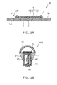
- FIGS. 1A and 1B are schematic cross-sectional views illustrating a light emitting module 10 and a lighting device 100 according to the embodiment.
- FIG. 1A illustrates the light emitting module 10
- FIG. 1B illustrates the lighting device 100 in which the light emitting module is embedded.
- the light emitting module 10 includes a substrate 3, a light emitting body 5 disposed on the substrate 3, and a phosphor layer 9.
- the phosphor layer 9 includes a first phosphor and a second phosphor which are excited by emitted light of the light emitting body 5.
- the first phosphor is a red phosphor 15 emitting red light.
- the second phosphor has a light emitting peak in the wavelength band between the peak wavelength of the light emitting spectrum of the light emitting body 5 and the peak wavelength of the light emitting spectrum of the red phosphor 15.
- a yellow phosphor 17 emitting yellow light As the second phosphor, a green phosphor may be used, and the yellow phosphor and the green phosphor may be mixed together for use.
- the substrate 3 is a ceramic substrate.
- the light emitting body 5 emits the light of 400 to 480 nanometers (nm) in the wavelength, and excites the red phosphor 15 and the yellow phosphor 17.
- the light emitting body 5 is a Light Emitting Diode (LED) and for example, emits blue light of 450 to 460 nm in a dominant wavelength.
- LED Light Emitting Diode
- the light emitting body 5 is mounted on an upper surface 3a of the substrate 3 via an adhesive.
- Multiple light emitting bodies 5 are mounted on the substrate 3, and are connected to each other in series or in parallel using a metal wire.
- a bank 7 is disposed so as to surround the periphery of a region on which the multiple light emitting bodies 5 are mounted.
- the bank 7 includes a white resin.
- the red phosphor 15 includes a phosphor represented by a chemical formula of K 2 SiF 6 :Mn, and for example, the yellow phosphor 17 is a YAG phosphor.
- the light emitting module 10 is embedded in the lighting device 100 as a light source.
- the lighting device 100 is an electric bulb type lamp, and includes the light emitting module 10, a housing 21 on which the light emitting module 10 is mounted, and a cover 30 covering the light emitting module 10.
- the lighting device 100 illustrated herein is one example, and thus, the embodiment is not limited thereto.
- a power conversion unit 40 supplying power to the light emitting module 10 is disposed inside the housing 21.
- the power conversion unit 40 is electrically connected to the light emitting module 10 and a socket 50 via lead wires 41 and 42.
- the power conversion unit 40 is accommodated in an insulating case 23 disposed inside the housing 21.
- the power conversion unit 40 receives AC power supply from a commercial power supply (not illustrated) via the socket 50, and for example, supplies the power to the light emitting module 10 by converting the AC power into DC power.
- the light emitting module 10 emits white light by receiving the power supply from the power conversion unit 40. That is, the white light is emitted by mixing the blue light emitted from the light emitting body 5, the red light emitted from the red phosphor 15 and the yellow light emitted from the yellow phosphor 17.
- FIGS. 2A to 4 are graphs illustrating the characteristics of the red phosphor 15 included in the phosphor layer 9.
- FIG. 2A is a graph illustrating a light emitting spectrum of a phosphor.
- a horizontal axis represents a light emitting wavelength ⁇ , and a vertical axis represents a light emitting intensity I L .
- a graph A in FIG. 2A illustrates the light emitting spectrum of the red phosphor 15, and a graph B illustrates the light emitting spectrum of a CASN phosphor according to a comparative example.
- the red phosphor 15 has light emitting peaks P 1 , P 2 and P 3 whose half-value width is 20 nm or less in the wavelength range from 610 nm to less than 650 nm.
- the light emitting intensity I L in the wavelength region of 650 nm or more is equal to or less than half of the light emitting peaks P 1 and P 2 .
- the CASN phosphor has the light emitting peaks in the wavelength range from 610 to 620 nm, and the half-value width reaches approximately 170 nm. Then, the light emitting intensity in the wavelength of 650 nm is approximately 80% of the light emitting intensity in the peak wavelength.
- the intensity of the light emitting spectrum in the wavelength band of 650 nm or more where relative visibility is reduced is lower than that of the CASN phosphor. Therefore, if the correlated color temperature and the average color rendering index are the same as each other, luminous flux of the light emitting module using the red phosphor 15 is larger than that of one using the CASN phosphor. That is, the luminous efficiency is high.
- FIG. 2B is a graph illustrating an excitation spectrum of a phosphor.
- the horizontal axis represents an excited-light wavelength ⁇ , and the vertical axis represents a relative light emitting intensity ⁇ E .
- the graph A in FIG. 2B illustrates the excitation spectrum of the red phosphor 15, and the graph B illustrates the excitation spectrum of a CASN phosphor according to a comparative example.
- the red phosphor 15 has an excitation band in the wavelength range from 300 nm to 550 nm, and has absorption peaks ⁇ 1 and ⁇ 2 of excited light in the vicinity of the wavelength of 350 nm and 450 nm.
- the CASN phosphor has a spectrum gradually decreasing from the wavelength of 300 nm toward a longer wavelength side, and has the excitation band in the wavelength range exceeding 600 nm from a wavelength side shorter than 300 nm.
- the excitation band represents a wavelength range where the phosphor absorbs energy of the excited light and emits the light.
- the absorption peak ⁇ 2 of the red phosphor 15 is overlapped with the peak wavelength of the light emitting spectrum of a blue LED. Then, the excitation band of the red phosphor 15 in the wavelength range of 500 nm or more is equal to or less than 10% of the absorption peak ⁇ 2 . That is, in the red phosphor 15, a long wavelength end of the excitation band is located in the vicinity of 500 nm. Accordingly, the red phosphor 15 efficiently absorbs the emitted light of the blue LED, but scarcely absorbs the emitted light of the yellow phosphor 17.
- the excitation band of the CASN phosphor is spread toward the longer wavelength side up to the wavelength exceeding 600 nm. Then, the CASN phosphor absorbs the emitted light of the yellow phosphor 17 and converts the light into the red light. That is, in the light emitting module using the CASN phosphor, output light thereof includes components to be absorbed by both of the yellow phosphor 17 and the CASN phosphor. For this reason, the luminous efficiency of the light emitting module is reduced.
- the long wavelength end of the excitation band of the first phosphor be located at the wavelength side shorter than the peak wavelength of the light emitting spectrum of the second phosphor.
- the excitation band of K 2 SiF 6 :Mn included in the red phosphor 15 according to the embodiment is located at the wavelength side shorter than 520 nm, and the emitted light of the yellow phosphor 17 and the green phosphor is scarcely absorbed. Therefore, it is possible to increase the luminous efficiency of the light emitting module 10 by using K 2 SiF 6 :Mn.
- the luminous efficiency when using the CASN phosphor is 83 lumens (Im)/watt (W).
- the luminous efficiency when using the red phosphor 15 including K 2 SiF 6 :Mn is 100 Im/W.
- the average color rendering index of the light emitting module using the CASN phosphor is 80
- the average color rendering index of the light emitting module using the red phosphor 15 is 90. That is, in the light emitting module using the red phosphor 15 including K 2 SiF 6 :Mn, it is possible to increase at least any one of the luminous efficiency and the average color rendering index Ra.
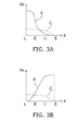
- FIGS. 3A and 3B are schematic views illustrating density distribution of a phosphor in a direction perpendicular to the substrate 3 of the phosphor layer 9 (X direction illustrated in FIG. 1A ).
- a graph A illustrates the density distribution of the red phosphor 15, and a graph C illustrates the density distribution of the yellow phosphor 17.
- FIG. 3A illustrates a case where an average particle diameter of the red phosphor 15 is larger than the average particle diameter of the yellow phosphor 17.
- FIG. 3B illustrates a case where the average particle diameter of the red phosphor 15 is the same as or smaller than an average particle diameter of the yellow phosphor 17.
- the translucent resin 13 which is a main component of the phosphor layer 9
- a thermosetting resin such as silicone
- viscosity of the translucent resin 13 during a curing process thereof is decreased by heating. Therefore, the red phosphor 15 and the yellow phosphor 17 which are dispersed in the translucent resin 13 are redistributed depending on particle diameters. For example, the phosphor having a large particle diameter is precipitated in the direction of the substrate 3, and the precipitation rate is faster as the particle diameter becomes larger.
- a density N F of the red phosphor 15 is a high density in a lower end LE side (substrate 3 side) of the distribution. Then, the distribution has a density gradient where the density N F is decreased in the direction of an upper end UE.
- the average particle diameter of the red phosphor 15 be equal to or more than 1.6 times the average particle diameter of the yellow phosphor 17. In this manner, it is possible to improve an absorption rate of the excited light by increasing the density of the red phosphor 15 of the substrate 3 side (light emitting body 5 side). As a result, as compared to a case where the red phosphors 15 are uniformly distributed on the phosphor layer 9, it is possible to reduce the content (weight percent: wt%). In addition, if the average particle diameter of the phosphor is large, the absorption rate of the excited light is high. From this point of view, it is possible to reduce the amount of the red phosphor 15 to be included in the phosphor layer 9. That is, it is possible to achieve cost reduction by reducing the amount of the red phosphor 15 to be used.
- the red phosphor 15 has the high density in the upper end UE side of the density distribution. Then, the distribution has the density gradient where the density N F is increased from the lower end LE in the direction of the upper end UE.
- the density of the red phosphor 15 may be increased in the upper end UE side of the distribution (upper end side of the phosphor layer 9). Accordingly, it is possible to reduce the content of the red phosphor 15 of the phosphor layer 9 by increasing the absorption rate of the excited light as compared to the case of uniformly distributing the red phosphor 15 on the phosphor layer 9. In addition, it is possible to reduce influence of temperature rising of the light emitting body 5 by distributing the red phosphor 15 on the upper end side of the phosphor layer 9 so as to be separated from the light emitting body 5.
- the density gradient of increasing the density toward at least any one of the upper end UE and the lower end LE it is preferable to have the density gradient of increasing the density toward at least any one of the upper end UE and the lower end LE. In this manner, it is possible to reduce manufacturing costs by suppressing the amount of the red phosphor 15 to be used.
- the average particle diameter of the red phosphor 15 is set to 10 ⁇ m and the average particle diameter of the red phosphor 15 is set to 16 ⁇ m, the content (weight percent: wt%) of the red phosphor 15 is approximately 5 times the content of the yellow phosphor 17. In contrast, if the average particle diameter of the red phosphor 15 is set to 45 ⁇ m, the content thereof is reduced to 3.8 times the content of the yellow phosphor 17.
- the CASN phosphor absorbs the emitted light of the yellow phosphor 17, since the excitation spectrum is spread up to the wavelength of 650 nm. Therefore, in order to achieve a desired correlated color temperature, it is necessary to increase the yellow phosphor 17 by the amount to compensate for the absorption of the CASN phosphor.
- the long wavelength end of the excitation spectrum is 520 nm. Therefore, the emitted light of the yellow phosphor 17 need not be absorbed and thus it is not necessary to compensate for the absorption. Therefore, it is possible to reduce the content of the yellow phosphor 17.
- the content (wt%) of the red phosphor 15 is equal to or more than 3 times the content (wt%) of the yellow phosphor 17.
- the correlated color temperature is 2,800 K
- the average particle diameter of the red phosphor 15 is set to 20 to 30 ⁇ m
- the content thereof is 6 to 7 times the content of the yellow phosphor 17 (YAG phosphor).
- FIG. 4 is a graph illustrating temperature characteristics of the red phosphor 15 according to the embodiment.
- the horizontal axis represents a temperature of the light emitting module 10 and the vertical axis represents relative intensity Ip of the light emitting peak of the red phosphor 15.
- the red phosphor 15 has multiple light emitting peaks P 1 , P 2 and P 3 in the wavelength range from 610 nm to less than 650 nm (refer to FIG. 2A ). These light emitting peaks respectively have the peak wavelength of 615 nm, 633 nm and 618 nm, corresponding to the light emitting peak of K 2 SiF 6 :Mn. Then, the half-value widths are respectively 20 nm or less.
- FIG. 4 illustrates a temperature change of the light emitting intensity in each light emitting peak, based on the light emitting intensity of 25°C.
- the light emitting intensity of the light emitting peak P 1 of the wavelength of 615 nm is not decreased in a temperature range from 25°C to 200°C, but is rather increased from 25°C to 100°C.
- the light emitting intensity of the light emitting peaks P 2 and P 3 in the peak wavelength of 633 nm and 648 nm is monotonically decreased along with the temperature rising, and is decreased to approximately 70% of 25°C at 200°C.
- the red phosphor 15 has a large stroke loss, and the temperature thereof is likely to rise. Therefore, if decrease in the light emitting intensity due to the temperature rising in the wavelength region where the relative visibility is high can be suppressed, it is possible to improve the temperature characteristics of the light emitting module 10. For example, in the light emitting module 10 using the red phosphor 15, it is possible to suppress temperature quenching in an operation for a large quantity of light.
- FIG. 5 is a schematic cross-sectional view of a light emitting module 20 according to a modification example of the embodiment.
- the light emitting module 20 includes the substrate 3, the light emitting body 5 disposed on the substrate 3, and the phosphor layer 9. Then, an intermediate layer 19 covering the light emitting body 5 is further provided on the substrate 3. The phosphor layer 9 is disposed on the intermediate layer 19. The intermediate layer 19 allows the emitted light of the light emitting body 5 to be transmitted.
- transmission is not limited to the transmission of all the emitted light of the light emitting body 5, but includes a case of absorbing a portion thereof.
- the intermediate layer 19 is a translucent resin such as silicone, and includes translucent inorganic oxide or glass.
- the intermediate layer 19 contains, for example, 20 wt% or more of the translucent inorganic oxide or the glass.
- the light emitting body 5 is directly covered with the phosphor layer 9. Accordingly, the light emitting of the red phosphor 15 and the yellow phosphor 17 in the phosphor layer 9 is influenced by the temperature rising of the light emitting body 5.
- the intermediate layer 19 isolates the phosphor layer 9 from the light emitting body 5. In this manner, it is possible to suppress, for example, the decrease in the luminous efficiency of each phosphor or the rising of the correlated color temperature by reducing the influence of the temperature rising of the light emitting body 5.
- the light emitting module adopts the red phosphor 15 which does not emit the light in the wavelength region of 650 nm or more where the relative visibility is low and further does not absorb the emitted light in a visible light region where the visibility is high. In this manner, color rendering properties are improved, thereby enabling the high luminous efficiency to be obtained in the module of the low correlated color temperature.
- the density distribution of the red phosphor 15 is controlled so that the density is increased on at least any one side of the upper end and the lower end thereof. In this manner, it is possible to achieve the cost reduction of the light emitting module by reducing the content of the red phosphor 15.
Landscapes
- Led Device Packages (AREA)
- Luminescent Compositions (AREA)
- Non-Portable Lighting Devices Or Systems Thereof (AREA)
Abstract
A light emitting module according to one embodiment includes a substrate (3); a light emitting body (5) disposed on the substrate (3); and a phosphor layer (9) having a first phosphor (15) and a second phosphor (17) which are excited by emitted light of the light emitting body (5). The first phosphor (15) has a light emitting peak whose half-value width is 20 nm or less in a wavelength range from 610 nm to less than 650 nm, and the second phosphor (17) has the light emitting peak in the wavelength range between a peak wavelength of a light emitting spectrum of the light emitting body (5) and the peak wavelength of the light emitting spectrum of the first phosphor (15). Then, a distribution of the first phosphor (15) in the phosphor layer (9) has density gradient, where the density of the first phosphor (15) increases toward at least one end of the phosphor layer (9) in a direction perpendicular to the substrate (3).

Description
- Embodiments described herein relate generally to a light emitting module and a lighting device.
- Most light emitting modules used as a light source of lighting equipment include a blue light emitting element and a phosphor which is excited by emitted light from the blue light emitting element, and output white light obtained by combining blue light emitted from the blue light emitting element and longer wavelength light emitted from the phosphor. Then, for the phosphor converting the blue light into the long wavelength light, it is desirable to use a phosphor which has a high luminous efficiency and exhibits less decrease of luminous flux as increasing ambient temperature. For example, in view of such characteristics, a YAG phosphor emitting yellow light and a CASN phosphor emitting red light are used.
-
-
FIGS. 1A and 1B are schematic cross-sectional views illustrating a light emitting module and a lighting device according to an embodiment; -
FIGS. 2A and 2B are graphs illustrating characteristics of a phosphor according to the embodiment; -
FIGS. 3A and 3B are schematic diagrams illustrating distribution of a phosphor according to the embodiment; -
FIG. 4 is a graph illustrating temperature characteristics of a phosphor according to the embodiment; and -
FIG. 5 is a schematic cross-sectional view illustrating a light emitting module according to a modification example of the embodiment. - A light emitting module according to one embodiment includes a substrate; a light emitting body disposed on the substrate; and a phosphor layer having a first phosphor and a second phosphor which are excited by emitted light of the light emitting body. The first phosphor has a light emitting peak whose half-value width is 20 nm or less in a wavelength range from 610 nm to less than 650 nm, and the second phosphor has a light emitting peak in the wavelength range between a peak wavelength of a light emitting spectrum of the light emitting body and the peak wavelength of the light emitting spectrum of the first phosphor. Then, a distribution of the first phosphor in the phosphor layer has density gradient, where the density of the first phosphor increases toward at least one end of the phosphor layer in a direction perpendicular to the substrate.
- The light emitting spectrum of a CASN or SCASN phosphor used as a red phosphor includes a wavelength band of low relative visibility exceeding 650 nm, and a long wavelength end of an excitation band exceeds 600 nm. That is, there is an aspect of absorbing light in a wavelength region of high relative visibility and emitting the light of the low relative visibility. Therefore, in the light emitting module containing many red phosphors and having a low correlated color temperature, average color rendering index and luminous efficiency are reduced. Accordingly, one embodiment provides a light emitting module and a lighting device which can improve color rendering properties and the luminous efficiency.
- Hereinafter, the embodiment will be described with reference to the drawings. The same reference numerals are given to the same elements in the drawing, and detailed description thereof will be appropriately omitted, and different elements will be described. The drawings are schematically and conceptually prepared, and thus, a relationship between a thickness and a width of each element and a ratio of sizes between the elements are not necessarily limited to real things. In addition, even if the same element is represented, in some cases, the element may be represented by mutually different dimensions or ratios depending on the drawing.
-
FIGS. 1A and 1B are schematic cross-sectional views illustrating alight emitting module 10 and alighting device 100 according to the embodiment.FIG. 1A illustrates thelight emitting module 10 andFIG. 1B illustrates thelighting device 100 in which the light emitting module is embedded. - As illustrated in
FIG. 1A , thelight emitting module 10 includes asubstrate 3, alight emitting body 5 disposed on thesubstrate 3, and aphosphor layer 9. Thephosphor layer 9 includes a first phosphor and a second phosphor which are excited by emitted light of thelight emitting body 5. - The first phosphor is a
red phosphor 15 emitting red light. The second phosphor has a light emitting peak in the wavelength band between the peak wavelength of the light emitting spectrum of thelight emitting body 5 and the peak wavelength of the light emitting spectrum of thered phosphor 15. Hereinafter, an example will be described using ayellow phosphor 17 emitting yellow light as the second phosphor, but is not limited thereto. For example, as the second phosphor, a green phosphor may be used, and the yellow phosphor and the green phosphor may be mixed together for use. - For example, the
substrate 3 is a ceramic substrate. Thelight emitting body 5 emits the light of 400 to 480 nanometers (nm) in the wavelength, and excites thered phosphor 15 and theyellow phosphor 17. Specifically, thelight emitting body 5 is a Light Emitting Diode (LED) and for example, emits blue light of 450 to 460 nm in a dominant wavelength. - For example, the
light emitting body 5 is mounted on anupper surface 3a of thesubstrate 3 via an adhesive. Multiplelight emitting bodies 5 are mounted on thesubstrate 3, and are connected to each other in series or in parallel using a metal wire. Then, abank 7 is disposed so as to surround the periphery of a region on which the multiplelight emitting bodies 5 are mounted. For example, thebank 7 includes a white resin. - Further, a
translucent resin 13 in which thered phosphor 15 and theyellow phosphor 17 are dispersed together is poured and cured inside thebank 7. In this manner, thephosphor layer 9 covering thelight emitting body 5 is disposed. For example, thered phosphor 15 includes a phosphor represented by a chemical formula of K2SiF6:Mn, and for example, theyellow phosphor 17 is a YAG phosphor. - For example, the
light emitting module 10 is embedded in thelighting device 100 as a light source. As illustrated inFIG. 1B , for example, thelighting device 100 is an electric bulb type lamp, and includes thelight emitting module 10, ahousing 21 on which thelight emitting module 10 is mounted, and acover 30 covering thelight emitting module 10. Thelighting device 100 illustrated herein is one example, and thus, the embodiment is not limited thereto. - A
power conversion unit 40 supplying power to thelight emitting module 10 is disposed inside thehousing 21. Thepower conversion unit 40 is electrically connected to thelight emitting module 10 and asocket 50 vialead wires power conversion unit 40 is accommodated in aninsulating case 23 disposed inside thehousing 21. Thepower conversion unit 40 receives AC power supply from a commercial power supply (not illustrated) via thesocket 50, and for example, supplies the power to thelight emitting module 10 by converting the AC power into DC power. - The
light emitting module 10 emits white light by receiving the power supply from thepower conversion unit 40. That is, the white light is emitted by mixing the blue light emitted from thelight emitting body 5, the red light emitted from thered phosphor 15 and the yellow light emitted from theyellow phosphor 17. - Next, referring to
FIGS. 2A to 4 , characteristics of thelight emitting module 10 will be described.FIGS. 2A to 4 are graphs illustrating the characteristics of thered phosphor 15 included in thephosphor layer 9. -
FIG. 2A is a graph illustrating a light emitting spectrum of a phosphor. A horizontal axis represents a light emitting wavelength λ, and a vertical axis represents a light emitting intensity IL. A graph A inFIG. 2A illustrates the light emitting spectrum of thered phosphor 15, and a graph B illustrates the light emitting spectrum of a CASN phosphor according to a comparative example. - As illustrated in the graph A, the
red phosphor 15 has light emitting peaks P1, P2 and P3 whose half-value width is 20 nm or less in the wavelength range from 610 nm to less than 650 nm. In addition, the light emitting intensity IL in the wavelength region of 650 nm or more is equal to or less than half of the light emitting peaks P1 and P2. In contrast, as illustrated in graph B, the CASN phosphor has the light emitting peaks in the wavelength range from 610 to 620 nm, and the half-value width reaches approximately 170 nm. Then, the light emitting intensity in the wavelength of 650 nm is approximately 80% of the light emitting intensity in the peak wavelength. - In the
red phosphor 15 according to the present embodiment, the intensity of the light emitting spectrum in the wavelength band of 650 nm or more where relative visibility is reduced is lower than that of the CASN phosphor. Therefore, if the correlated color temperature and the average color rendering index are the same as each other, luminous flux of the light emitting module using thered phosphor 15 is larger than that of one using the CASN phosphor. That is, the luminous efficiency is high. -
FIG. 2B is a graph illustrating an excitation spectrum of a phosphor. The horizontal axis represents an excited-light wavelength λ, and the vertical axis represents a relative light emitting intensity αE. The graph A inFIG. 2B illustrates the excitation spectrum of thered phosphor 15, and the graph B illustrates the excitation spectrum of a CASN phosphor according to a comparative example. - As illustrated in the graph A, the
red phosphor 15 has an excitation band in the wavelength range from 300 nm to 550 nm, and has absorption peaks α1 and α2 of excited light in the vicinity of the wavelength of 350 nm and 450 nm. In contrast, as illustrated in the graph B, for example, the CASN phosphor has a spectrum gradually decreasing from the wavelength of 300 nm toward a longer wavelength side, and has the excitation band in the wavelength range exceeding 600 nm from a wavelength side shorter than 300 nm. - Here, the excitation band represents a wavelength range where the phosphor absorbs energy of the excited light and emits the light.
- The absorption peak α2 of the
red phosphor 15 is overlapped with the peak wavelength of the light emitting spectrum of a blue LED. Then, the excitation band of thered phosphor 15 in the wavelength range of 500 nm or more is equal to or less than 10% of the absorption peak α2. That is, in thered phosphor 15, a long wavelength end of the excitation band is located in the vicinity of 500 nm. Accordingly, thered phosphor 15 efficiently absorbs the emitted light of the blue LED, but scarcely absorbs the emitted light of theyellow phosphor 17. - In contrast, the excitation band of the CASN phosphor is spread toward the longer wavelength side up to the wavelength exceeding 600 nm. Then, the CASN phosphor absorbs the emitted light of the
yellow phosphor 17 and converts the light into the red light. That is, in the light emitting module using the CASN phosphor, output light thereof includes components to be absorbed by both of theyellow phosphor 17 and the CASN phosphor. For this reason, the luminous efficiency of the light emitting module is reduced. - Thus, it is desirable that the long wavelength end of the excitation band of the first phosphor be located at the wavelength side shorter than the peak wavelength of the light emitting spectrum of the second phosphor. The excitation band of K2SiF6:Mn included in the
red phosphor 15 according to the embodiment is located at the wavelength side shorter than 520 nm, and the emitted light of theyellow phosphor 17 and the green phosphor is scarcely absorbed. Therefore, it is possible to increase the luminous efficiency of thelight emitting module 10 by using K2SiF6:Mn. - For example, if compared by using the light emitting module of the average color rendering index of Ra 80 and the correlated color temperature of 2800 Kelvin (K), the luminous efficiency when using the CASN phosphor is 83 lumens (Im)/watt (W). In contrast, the luminous efficiency when using the
red phosphor 15 including K2SiF6:Mn is 100 Im/W. In addition, when the same luminous efficiency is set, whereas the average color rendering index of the light emitting module using the CASN phosphor is 80, the average color rendering index of the light emitting module using thered phosphor 15 is 90. That is, in the light emitting module using thered phosphor 15 including K2SiF6:Mn, it is possible to increase at least any one of the luminous efficiency and the average color rendering index Ra. -
FIGS. 3A and 3B are schematic views illustrating density distribution of a phosphor in a direction perpendicular to thesubstrate 3 of the phosphor layer 9 (X direction illustrated inFIG. 1A ). A graph A illustrates the density distribution of thered phosphor 15, and a graph C illustrates the density distribution of theyellow phosphor 17.FIG. 3A illustrates a case where an average particle diameter of thered phosphor 15 is larger than the average particle diameter of theyellow phosphor 17.FIG. 3B illustrates a case where the average particle diameter of thered phosphor 15 is the same as or smaller than an average particle diameter of theyellow phosphor 17. - As the
translucent resin 13 which is a main component of thephosphor layer 9, for example, a thermosetting resin such as silicone is used. Then, viscosity of thetranslucent resin 13 during a curing process thereof is decreased by heating. Therefore, thered phosphor 15 and theyellow phosphor 17 which are dispersed in thetranslucent resin 13 are redistributed depending on particle diameters. For example, the phosphor having a large particle diameter is precipitated in the direction of thesubstrate 3, and the precipitation rate is faster as the particle diameter becomes larger. - Therefore, as illustrated in the graph A of
FIG. 3A , when the average particle diameter of thered phosphor 15 is larger than that of theyellow phosphor 17, thered phosphor 15 is more precipitated on thesubstrate 3 side. Accordingly, a density NF of thered phosphor 15 is a high density in a lower end LE side (substrate 3 side) of the distribution. Then, the distribution has a density gradient where the density NF is decreased in the direction of an upper end UE. - For example, it is preferable that the average particle diameter of the
red phosphor 15 be equal to or more than 1.6 times the average particle diameter of theyellow phosphor 17. In this manner, it is possible to improve an absorption rate of the excited light by increasing the density of thered phosphor 15 of thesubstrate 3 side (light emitting body 5 side). As a result, as compared to a case where thered phosphors 15 are uniformly distributed on thephosphor layer 9, it is possible to reduce the content (weight percent: wt%). In addition, if the average particle diameter of the phosphor is large, the absorption rate of the excited light is high. From this point of view, it is possible to reduce the amount of thered phosphor 15 to be included in thephosphor layer 9. That is, it is possible to achieve cost reduction by reducing the amount of thered phosphor 15 to be used. - In contrast, when the average particle diameter of the
red phosphor 15 is the same as or smaller than that of theyellow phosphor 17, precipitation of thered phosphor 15 is suppressed. For example, specific gravity of K2SiF6:Mn is less weighed than the specific gravity of the YAG phosphor. Therefore, as illustrated inFIG. 3B , thered phosphor 15 has the high density in the upper end UE side of the density distribution. Then, the distribution has the density gradient where the density NF is increased from the lower end LE in the direction of the upper end UE. - In this manner, the density of the
red phosphor 15 may be increased in the upper end UE side of the distribution (upper end side of the phosphor layer 9). Accordingly, it is possible to reduce the content of thered phosphor 15 of thephosphor layer 9 by increasing the absorption rate of the excited light as compared to the case of uniformly distributing thered phosphor 15 on thephosphor layer 9. In addition, it is possible to reduce influence of temperature rising of thelight emitting body 5 by distributing thered phosphor 15 on the upper end side of thephosphor layer 9 so as to be separated from thelight emitting body 5. - As described above, in the density distribution in a direction perpendicular to the
substrate 3 of thered phosphor 15, it is preferable to have the density gradient of increasing the density toward at least any one of the upper end UE and the lower end LE. In this manner, it is possible to reduce manufacturing costs by suppressing the amount of thered phosphor 15 to be used. - Further, it is possible to reduce the amount to be used by increasing the average particle diameter of the
red phosphor 15. For example, in the light emitting module including the blue LED as thelight emitting body 5, when the correlated color temperature is set to 2,800 K, if the average particle diameter of theyellow phosphor 17 is set to 10 µm and the average particle diameter of thered phosphor 15 is set to 16 µm, the content (weight percent: wt%) of thered phosphor 15 is approximately 5 times the content of theyellow phosphor 17. In contrast, if the average particle diameter of thered phosphor 15 is set to 45 µm, the content thereof is reduced to 3.8 times the content of theyellow phosphor 17. - In addition, it is possible to reduce the amount of the
yellow phosphor 17 to be used by using thered phosphor 15 according to the present embodiment. For example, the CASN phosphor absorbs the emitted light of theyellow phosphor 17, since the excitation spectrum is spread up to the wavelength of 650 nm. Therefore, in order to achieve a desired correlated color temperature, it is necessary to increase theyellow phosphor 17 by the amount to compensate for the absorption of the CASN phosphor. - On the other hand, in K2SiF6:Mn included in the
red phosphor 15 according to the present embodiment, the long wavelength end of the excitation spectrum is 520 nm. Therefore, the emitted light of theyellow phosphor 17 need not be absorbed and thus it is not necessary to compensate for the absorption. Therefore, it is possible to reduce the content of theyellow phosphor 17. For example, in the light emitting module where the correlated color temperature is 3,000 K or less, the content (wt%) of thered phosphor 15 is equal to or more than 3 times the content (wt%) of theyellow phosphor 17. For example, in the light emitting module where the correlated color temperature is 2,800 K, when the average particle diameter of thered phosphor 15 is set to 20 to 30 µm, the content thereof is 6 to 7 times the content of the yellow phosphor 17 (YAG phosphor). -
FIG. 4 is a graph illustrating temperature characteristics of thered phosphor 15 according to the embodiment. The horizontal axis represents a temperature of thelight emitting module 10 and the vertical axis represents relative intensity Ip of the light emitting peak of thered phosphor 15. - The
red phosphor 15 has multiple light emitting peaks P1, P2 and P3 in the wavelength range from 610 nm to less than 650 nm (refer toFIG. 2A ). These light emitting peaks respectively have the peak wavelength of 615 nm, 633 nm and 618 nm, corresponding to the light emitting peak of K2SiF6:Mn. Then, the half-value widths are respectively 20 nm or less. -
FIG. 4 illustrates a temperature change of the light emitting intensity in each light emitting peak, based on the light emitting intensity of 25°C. As illustrated inFIG. 4 , the light emitting intensity of the light emitting peak P1 of the wavelength of 615 nm is not decreased in a temperature range from 25°C to 200°C, but is rather increased from 25°C to 100°C. On the other hand, the light emitting intensity of the light emitting peaks P2 and P3 in the peak wavelength of 633 nm and 648 nm is monotonically decreased along with the temperature rising, and is decreased to approximately 70% of 25°C at 200°C. - Human relative visibility reaches a peak in the wavelength of 555 nm, and is decreased as the wavelength is longer. Therefore, in the
red phosphor 15, the light emitting intensity of the light emitting peak P1 in the peak wavelength of 615 nm where the relative visibility is high is not decreased in contrast to the temperature rising of the module. On the other hand, in the light emitting peaks P2 and P3 where the temperature change of the light emitting intensity is considerable, the visibility is low. Therefore, when considering the relative visibility, the temperature change of the light emitting intensity of thered phosphor 15 is suppressed. - In addition, the
red phosphor 15 has a large stroke loss, and the temperature thereof is likely to rise. Therefore, if decrease in the light emitting intensity due to the temperature rising in the wavelength region where the relative visibility is high can be suppressed, it is possible to improve the temperature characteristics of thelight emitting module 10. For example, in thelight emitting module 10 using thered phosphor 15, it is possible to suppress temperature quenching in an operation for a large quantity of light. -
FIG. 5 is a schematic cross-sectional view of alight emitting module 20 according to a modification example of the embodiment. As illustrated inFIG. 5 , thelight emitting module 20 includes thesubstrate 3, thelight emitting body 5 disposed on thesubstrate 3, and thephosphor layer 9. Then, anintermediate layer 19 covering thelight emitting body 5 is further provided on thesubstrate 3. Thephosphor layer 9 is disposed on theintermediate layer 19. Theintermediate layer 19 allows the emitted light of thelight emitting body 5 to be transmitted. Here, the term "transmission" is not limited to the transmission of all the emitted light of thelight emitting body 5, but includes a case of absorbing a portion thereof. - For example, the
intermediate layer 19 is a translucent resin such as silicone, and includes translucent inorganic oxide or glass. In addition, theintermediate layer 19 contains, for example, 20 wt% or more of the translucent inorganic oxide or the glass. - For example, in the
light emitting module 10 illustrated inFIG. 1A , thelight emitting body 5 is directly covered with thephosphor layer 9. Accordingly, the light emitting of thered phosphor 15 and theyellow phosphor 17 in thephosphor layer 9 is influenced by the temperature rising of thelight emitting body 5. In contrast, in thelight emitting module 20, theintermediate layer 19 isolates thephosphor layer 9 from thelight emitting body 5. In this manner, it is possible to suppress, for example, the decrease in the luminous efficiency of each phosphor or the rising of the correlated color temperature by reducing the influence of the temperature rising of thelight emitting body 5. - As described above, the light emitting module according to the present embodiments adopts the
red phosphor 15 which does not emit the light in the wavelength region of 650 nm or more where the relative visibility is low and further does not absorb the emitted light in a visible light region where the visibility is high. In this manner, color rendering properties are improved, thereby enabling the high luminous efficiency to be obtained in the module of the low correlated color temperature. In addition, in thephosphor layer 9, the density distribution of thered phosphor 15 is controlled so that the density is increased on at least any one side of the upper end and the lower end thereof. In this manner, it is possible to achieve the cost reduction of the light emitting module by reducing the content of thered phosphor 15. - While certain embodiments have been described, these embodiments have been presented by way of example only, and are not intended to limit the scope of the inventions. Indeed, the novel embodiments described herein may be embodied in a variety of other forms; furthermore, various omissions, substitutions and changes in the form of the embodiments described herein may be made without departing from the spirit of the inventions. The accompanying claims and their equivalents are intended to cover such forms or modifications as would fall within the scope of the invention.
Claims (15)
- A light emitting module comprising:a substrate (3);a light emitting body (5) disposed on the substrate (3); anda phosphor layer (9) having a first phosphor (15) and a second phosphor (17) which are excited by emitted light of the light emitting body (5), the first phosphor (15) having a light emitting peak whose half-value width is 20 nm or less in a wavelength range from 610 nm to less than 650 nm, the second phosphor (17) having the light emitting peak in the wavelength range between a peak wavelength of a light emitting spectrum of the light emitting body (5) and the peak wavelength of the light emitting spectrum of the first phosphor (15), and a distribution of the first phosphor (15) in the phosphor layer (9) having density gradient, where the density of the first phosphor increases toward at least one end of the phosphor layer (9) in a direction perpendicular to the substrate (3).
- The module according to claim 1,
wherein an average particle diameter of the first phosphor (15) is larger than an average particle diameter of the second phosphor (17), and
the first phosphor (15) is disposed so that the density of the first phosphor (15) increases toward the substrate (3). - The module according to claim 2,
wherein the average particle diameter of the first phosphor (15) is 1.6 or more times the average particle diameter of the second phosphor (17). - The module according to claim 1,
wherein the average particle diameter of the first phosphor (15) is the same as or smaller than the average particle diameter of the second phosphor (17), and
the first phosphor (15) is disposed so that the density of the first phosphor (15) increases as increasing separation from the substrate (3). - The module according to any one of claims 1 to 4,
wherein light emitting intensity in a wavelength region of 650 nm or more of the first phosphor (15) is equal to or less than half of intensity of the light emitting peak. - The module according to any one of claims 1 to 5,
wherein the first phosphor (15) has multiple light emitting peaks in the wavelength range from 610 nm to less than 650 nm, and
a temperature change of light emitting intensity in the light emitting peak located in a shorter wavelength side among the multiple light emitting peaks is smaller than the temperature change of the light emitting intensity in the light emitting peak located in a longer wavelength side. - The module according to any one of claims 1 to 6,
wherein the first phosphor (15) has an excitation band in the wavelength range from 300 nm to 550 nm, and has an absorption peak of excitation light in a wavelength range between 350 nm and 450 nm. - The module according to claim 7,
wherein intensity of the excitation band of the first phosphor (15) in the wavelength range of 500 nm or more is equal to or less than 10% of the intensity of the absorption peak. - The module according to any one of claims 1 to 8,
wherein content of the first phosphor (15) is equal to or more than three times the content of the second phosphor (17). - The module according to claim 9,
wherein the content of the first phosphor (15) is from 3.8 times to 5 times content of the second phosphor (17). - The module according to any one of claims 1 to 10,
wherein the first phosphor (15) includes a phosphor represented by a chemical formula of K2SiF6:Mn. - The module according to any one of claims 1 to 11,
wherein the light emitting body (5) emits light in a wavelength range from 400 nm to 480 nm. - The module according to any one of claims 1 to 12, further comprising:an intermediate layer (19) covering the light emitting body (5) on the substrate (3) and allowing the emitted light of the light emitting body (5) to be transmitted,wherein the phosphor layer (9) is disposed on the intermediate layer (19).
- The module according to claim 13,
wherein the intermediate layer (19) includes at least any one of translucent inorganic oxide and glass. - A lighting device comprising:the light emitting module (10) according to any one of claims 1 to 14; anda housing (21) on which the light emitting module is mounted.
Applications Claiming Priority (1)
| Application Number | Priority Date | Filing Date | Title |
|---|---|---|---|
| JP2013032644A JP2014165225A (en) | 2013-02-21 | 2013-02-21 | Light-emitting module and illuminating device |
Publications (1)
| Publication Number | Publication Date |
|---|---|
| EP2770546A2 true EP2770546A2 (en) | 2014-08-27 |
Family
ID=49182161
Family Applications (1)
| Application Number | Title | Priority Date | Filing Date |
|---|---|---|---|
| EP13184905.1A Withdrawn EP2770546A2 (en) | 2013-02-21 | 2013-09-18 | Light emitting module and lighting device |
Country Status (5)
| Country | Link |
|---|---|
| US (1) | US8952607B2 (en) |
| EP (1) | EP2770546A2 (en) |
| JP (1) | JP2014165225A (en) |
| CN (1) | CN104009148A (en) |
| TW (1) | TW201433755A (en) |
Families Citing this family (5)
| Publication number | Priority date | Publication date | Assignee | Title |
|---|---|---|---|---|
| KR102191211B1 (en) * | 2014-02-28 | 2020-12-15 | 서울반도체 주식회사 | Light emitting diode package |
| JP6472728B2 (en) | 2015-08-04 | 2019-02-20 | 日亜化学工業株式会社 | LIGHT EMITTING DEVICE AND BACKLIGHT WITH LIGHT EMITTING DEVICE |
| JP6447557B2 (en) * | 2016-03-24 | 2019-01-09 | 日亜化学工業株式会社 | Method for manufacturing light emitting device |
| TWI757315B (en) * | 2017-07-28 | 2022-03-11 | 晶元光電股份有限公司 | Light-emitting device and manufacturing method thereof |
| EP4449512A4 (en) * | 2021-12-14 | 2026-01-14 | Lumileds Llc | COLOR-COUNTABLE LIGHT-EMISSIVING DEVICES |
Family Cites Families (23)
| Publication number | Priority date | Publication date | Assignee | Title |
|---|---|---|---|---|
| US6252254B1 (en) * | 1998-02-06 | 2001-06-26 | General Electric Company | Light emitting device with phosphor composition |
| JP4296644B2 (en) * | 1999-01-29 | 2009-07-15 | 豊田合成株式会社 | Light emitting diode |
| JP2003179269A (en) * | 2001-01-24 | 2003-06-27 | Nichia Chem Ind Ltd | Optical semiconductor device |
| MY145695A (en) * | 2001-01-24 | 2012-03-30 | Nichia Corp | Light emitting diode, optical semiconductor device, epoxy resin composition suited for optical semiconductor device, and method for manufacturing the same |
| JP2004055138A (en) * | 2001-12-13 | 2004-02-19 | Nobuyuki Fujikawa | All types of DC bulbs with semi-permanent DC current variation voltage and shock resistant and low power consumption design |
| CN1641897A (en) * | 2004-01-14 | 2005-07-20 | 诠兴开发科技股份有限公司 | Improvement method of white light LED |
| JP2005244075A (en) * | 2004-02-27 | 2005-09-08 | Matsushita Electric Works Ltd | Light emitting device |
| JP4729281B2 (en) * | 2004-09-13 | 2011-07-20 | 株式会社フジクラ | Light emitting diode and light emitting diode manufacturing method |
| US7497973B2 (en) | 2005-02-02 | 2009-03-03 | Lumination Llc | Red line emitting phosphor materials for use in LED applications |
| JP4473285B2 (en) * | 2006-03-31 | 2010-06-02 | Dowaエレクトロニクス株式会社 | Light emitting device and manufacturing method thereof |
| JP2008027979A (en) * | 2006-07-18 | 2008-02-07 | Lumi Tech:Kk | Light emitting device |
| JP5428147B2 (en) * | 2006-12-07 | 2014-02-26 | 三菱化学株式会社 | Organic phosphor material |
| JP2009019163A (en) * | 2007-07-13 | 2009-01-29 | Sharp Corp | Phosphor particle assembly for light emitting device, light emitting device, and backlight device for liquid crystal display |
| JP2010287680A (en) * | 2009-06-10 | 2010-12-24 | Mitsubishi Chemicals Corp | Light emitting device |
| JP5446511B2 (en) * | 2009-06-30 | 2014-03-19 | 三菱化学株式会社 | Phosphor and method for producing the same, phosphor-containing composition and light emitting device using the phosphor, and image display device and lighting device using the light emitting device |
| JP2012015330A (en) * | 2010-06-30 | 2012-01-19 | Toshiba Lighting & Technology Corp | Light emitting module and lighting system |
| US8057706B1 (en) * | 2010-07-27 | 2011-11-15 | General Electric Company | Moisture-resistant phosphor and associated method |
| CN201829530U (en) * | 2010-09-02 | 2011-05-11 | 深圳市海隆兴光电子有限公司 | Light-source lamp of light emitting diode (LED) white light emitting diode |
| JP5273108B2 (en) * | 2010-09-06 | 2013-08-28 | 三菱化学株式会社 | LIGHT EMITTING ELEMENT, LIGHTING DEVICE USING SAME, AND IMAGE DISPLAY DEVICE |
| JP2013201274A (en) * | 2012-03-23 | 2013-10-03 | Toshiba Lighting & Technology Corp | Luminaire |
| JP6094254B2 (en) * | 2013-02-21 | 2017-03-15 | 東芝ライテック株式会社 | Light emitting module and lighting device |
| US9698314B2 (en) * | 2013-03-15 | 2017-07-04 | General Electric Company | Color stable red-emitting phosphors |
| US9580648B2 (en) * | 2013-03-15 | 2017-02-28 | General Electric Company | Color stable red-emitting phosphors |
-
2013
- 2013-02-21 JP JP2013032644A patent/JP2014165225A/en active Pending
- 2013-09-16 CN CN201310421507.XA patent/CN104009148A/en active Pending
- 2013-09-17 TW TW102133714A patent/TW201433755A/en unknown
- 2013-09-18 EP EP13184905.1A patent/EP2770546A2/en not_active Withdrawn
- 2013-09-19 US US14/031,554 patent/US8952607B2/en not_active Expired - Fee Related
Non-Patent Citations (1)
| Title |
|---|
| None |
Also Published As
| Publication number | Publication date |
|---|---|
| JP2014165225A (en) | 2014-09-08 |
| US20140232257A1 (en) | 2014-08-21 |
| CN104009148A (en) | 2014-08-27 |
| TW201433755A (en) | 2014-09-01 |
| US8952607B2 (en) | 2015-02-10 |
Similar Documents
| Publication | Publication Date | Title |
|---|---|---|
| CN103322511B (en) | Lighting device | |
| CN104521016B (en) | Phosphor converted LEDs, lamp and luminaire | |
| JP6365159B2 (en) | Light emitting device | |
| US8723412B2 (en) | White lighting device | |
| JP5956655B2 (en) | Yellow light emitting phosphor and light emitting device package using the same | |
| CN103080635B (en) | LED light bulb | |
| JP6855245B2 (en) | Fluorescent LED package | |
| EP2770547A2 (en) | Light emitting module and lighting device | |
| EP2869353A1 (en) | White light emitting device with adapted melatonin secretion | |
| US8952607B2 (en) | Light emitting module and lighting device | |
| US20100295069A1 (en) | High Luminous Flux Warm White Solid State Lighting Device | |
| US8519611B2 (en) | Hybrid illumination system with improved color quality | |
| TWI625380B (en) | Phosphor assembly for a light emitting device | |
| KR102244220B1 (en) | Semiconductor light emitting device | |
| JP6550889B2 (en) | Light emitting device and manufacturing method thereof | |
| US11901492B2 (en) | High color rendering white light emitting devices and high color rendering photoluminescence compositions | |
| CN121219527A (en) | LED filament |
Legal Events
| Date | Code | Title | Description |
|---|---|---|---|
| PUAI | Public reference made under article 153(3) epc to a published international application that has entered the european phase |
Free format text: ORIGINAL CODE: 0009012 |
|
| 17P | Request for examination filed |
Effective date: 20130918 |
|
| AK | Designated contracting states |
Kind code of ref document: A2 Designated state(s): AL AT BE BG CH CY CZ DE DK EE ES FI FR GB GR HR HU IE IS IT LI LT LU LV MC MK MT NL NO PL PT RO RS SE SI SK SM TR |
|
| AX | Request for extension of the european patent |
Extension state: BA ME |
|
| STAA | Information on the status of an ep patent application or granted ep patent |
Free format text: STATUS: THE APPLICATION HAS BEEN WITHDRAWN |
|
| 18W | Application withdrawn |
Effective date: 20150529 |