EP2770477A1 - Dynamically reconfigurable pipelined pre-processor - Google Patents
Dynamically reconfigurable pipelined pre-processor Download PDFInfo
- Publication number
- EP2770477A1 EP2770477A1 EP14164566.3A EP14164566A EP2770477A1 EP 2770477 A1 EP2770477 A1 EP 2770477A1 EP 14164566 A EP14164566 A EP 14164566A EP 2770477 A1 EP2770477 A1 EP 2770477A1
- Authority
- EP
- European Patent Office
- Prior art keywords
- module
- parameters
- pipeline
- processor
- control
- Prior art date
- Legal status (The legal status is an assumption and is not a legal conclusion. Google has not performed a legal analysis and makes no representation as to the accuracy of the status listed.)
- Granted
Links
Images





Classifications
-
- G—PHYSICS
- G06—COMPUTING OR CALCULATING; COUNTING
- G06T—IMAGE DATA PROCESSING OR GENERATION, IN GENERAL
- G06T1/00—General purpose image data processing
- G06T1/20—Processor architectures; Processor configuration, e.g. pipelining
-
- H—ELECTRICITY
- H04—ELECTRIC COMMUNICATION TECHNIQUE
- H04N—PICTORIAL COMMUNICATION, e.g. TELEVISION
- H04N19/00—Methods or arrangements for coding, decoding, compressing or decompressing digital video signals
- H04N19/85—Methods or arrangements for coding, decoding, compressing or decompressing digital video signals using pre-processing or post-processing specially adapted for video compression
Definitions
- a stream of video frames such as that generated by a video camera or read from a memory, frequently requires processing to improve the quality of the video or to extract features from the video.
- This processing is traditionally done by software in a post-processing operation.
- the post-processing operation may vary because (i) the parameters/coefficients of the algorithmic processing modules need to be modified; (ii) fine variations of a given algorithm need to be performed; and/or (iii) the operations that need to be performed on the video need to be changed.
- a software solution while versatile, is slow and expensive in terms of processing power.
- Hardware-based algorithms are typically faster and more efficient, but hardware, by its nature, is difficult to reconfigure quickly and easily, especially when it must keep pace with live, streaming video.
- Existing hardware-based image processing systems thus produce non-optimal results because of their limitations in flexibility.
- a pipelined video pre-processor is made up of several algorithmic transformation image-processing modules that may be connected to each other in a variety of different, customizable configurations. Each of these modules has a plurality of parameter registers that control finite variations of a given algorithm implementation.
- the parameters of the modules may be re-configured on a frame-by-frame basis with no loss of data, and the configuration of modules may be changed with minimal or no loss of data.
- the parameters may be changed via a connected processor, via DMA access, or both simultaneously.
- the differing control schemes are designed to be compatible with each other, ensuring seamless transitions between them.
- a pipelined video pre-processor includes a plurality of image-processing modules arranged in a pipeline.
- An input port receives configuration parameters for the plurality of modules, and an image-pipe controller decodes the configuration parameters.
- a shadow register applies the configuration parameters to the plurality of modules, thereby altering the image-processing characteristics of the modules.
- the pipeline may be a memory pipeline for processing image data from a memory or a camera pipeline for processing image data from a digital camera.
- One or more additional pipelines may be included.
- the configuration parameters may be received from a processor or a direct-memory access (“DMA") engine.
- the configuration parameters may be arranged in a memory in a block-control structure and are accessed via a DMA channel; the block-control structure may include a block-control header and one or more block-control words.
- the offsets of the block-control words in the block-control structure may correspond to addresses in a memory-mapped register ("MMR") space.
- the configuration parameters may be applied to a first frame of video data, and updated configuration parameters may be applied to a second frame of video data. Different pipeline stages in a module may receive the updated configuration parameters at different points in time in accordance with a data boundary.
- a method of processing image frames in a pipelined video pre-processor includes receiving configuration parameters for a plurality of image-processing modules in the pipelined video pre-processor.
- the configuration parameters may be stored in a shadow register and applied to the plurality of image-processing modules to thereby alter the image-processing characteristics of the modules.
- the configuration parameters may be received from a processor or a DMA engine; the modules may be arranged in one or more pipelines.
- the one or more pipelines may include a memory pipeline for processing image data from a memory or a camera pipeline for processing image data from a digital camera.
- the configuration parameters may be arranged in a memory in a block-control structure and may be accessed via a DMA channel.
- the block-control structure may include a block-control header and one or more block-control words.
- the offsets of the block-control words in the block-control structure may correspond to addresses in a memory-mapped register ("MMR") space.
- MMR memory-mapped register
- the configuration parameters may be applied to a first frame of video data and updated configuration parameters may be applied to a second frame of video data. Different pipeline stages in a module may receive the updated configuration parameters at different points in time in accordance with a data boundary.
- a pipelined video pre-processor in a digital-signal processor includes a plurality of image-processing modules arranged in a pipeline and an input port for receiving configuration parameters for the plurality of modules.
- An image-pipe controller decodes the configuration parameters, and a shadow register applies the configuration parameters to the plurality of modules, thereby altering the image-processing characteristics of the modules.
- the pipeline may be a memory pipeline for processing image data from a memory or a camera pipeline for processing image data from a digital camera.
- a system for configuring modules in a pipelined pre-processor includes a first input port for receiving a first control signal from a processor and a second input port for receiving a second control signal from a memory.
- An arbitration unit resolves a conflict between the first and second control signals.
- a controller decodes the first and second control signals and applies configuration parameters derived therefrom to the modules.
- An interface e.g., an advanced peripheral bus (“APB”) interface
- the first control signal may be a memory-mapped register (“MMR") input
- the second control signal may be received from one or more direct-memory access (“DMA”) channels.
- the first control signal may control a first subset of the modules and, simultaneously, the second control input may control a second subset of the modules.
- a module may be controlled by both the first and second control signals.
- a shadow register may receive one of the decoded first and second control signals.
- the shadow register may writes an application register in at least one module to thereby apply the configuration parameters to the module.
- the arbitration unit may stall the second control signal in the event of a conflict.
- a method for configuring modules in a pipelined pre-processor includes receiving a first control signal from a processor and a second control signal from a memory. A conflict is resolved between the first and second control signals. The first and second control signals are decoded, and configuration parameters derived therefrom are applied to the modules.
- a shadow register may be filled with information derived from one of the first or second control signals.
- a module may be configured in accordance with the contents of the shadow register.
- the first control signal may be ignored during configuring of the module.
- the second control signal may be stalled in the event of a conflict.
- the second control signal may be received from one or more DMA channels.
- the first control signal may control a first subset of the modules and, simultaneously, the second control input may control a second subset of the modules.
- a module may be controlled by both the first and second control signals.
- a pipelined video pre-processor having configurable modules in a digital-signal processor includes a first input port for receiving a first control signal from the digital-signal processor and a second input port for receiving a second control signal from a memory.
- An arbitration unit resolves a conflict between the first and second control signals.
- a controller decodes the first and second control signals and configuration parameters derived therefrom are applied to the modules.
- the first control signal may be an MMR input and the second control signal may be a DMA input.
- a system for programming reconfigurable modules in a pipelined video pre-processor includes an input port for receiving a block-control structure from a memory via a direct-memory access ("DMA") channel.
- An image-pipe controller decodes a block-control header in the block-control structure and selects a block-control word in the block-control structure in accordance with the decoded block-control header.
- a shadow register receives the block-control word and applies parameters in the block-control word to an application register in a reconfigurable module, thereby adjusting a parameter of the module.
- the block-control header may include a block address that uniquely identifies the module.
- the input port may further receive a block-control list comprising a plurality of block-control structures.
- the block-control header may include a word count that comprises a number of block-control structures.
- An order of the block-control structures may correspond to an order of modules in a pipeline.
- the block-control header may include an offset indicating which application register receives the block-control word. The offset may be equivalent to the difference between an memory-mapped register ("MMR") address of an application register in the module and an MMR base address of the module.
- the block-control header may include multiplexer-select information for specifying how the module connects to a second module.
- An offset of a block-control word intended for an application register may correspond to an address of the same application register in a memory-mapped register ("MMR") space. The offset of the block-control word may be obtained by shifting the address.
- a method for programming reconfigurable modules in a pipelined video pre-processor includes receiving a block-control structure from a memory via a direct-memory access (“DMA") channel and decoding a block-control header in the block-control structure.
- a block-control word in the block-control structure is selected in accordance with the decoded block-control header. Parameters in the block-control word are applied to an application register in a reconfigurable module, thereby adjusting a parameter of the module.
- DMA direct-memory access
- Decoding the block-control header may include decoding a block address that uniquely identifies the module.
- a block-control list comprising a plurality of block-control structures may be received.
- Decoding the block-control header may include decoding a word count that comprises a number of block-control structures.
- Block-control words in each of the block-control structures may be applied to each of a plurality of modules.
- An order of the block-control structures may correspond to an order of the modules in a pipe. Parameters in the block-control word may be applied to a multiplexer select to thereby configure a connection between two modules.
- a status register may be read from a module in accordance with a status count in the block-control header.
- a pipelined video pre-processor having a plurality of reconfigurable modules in a digital-signal processor includes an input port for receiving a block-control structure from a memory via a direct-memory access ("DMA") channel.
- An image-pipe controller decodes a block-control header in the block-control structure and selects a block-control word in the block-control structure in accordance with the decoded block-control header.
- a shadow register receives the block-control word and applies parameters in the block-control word to an application register in a reconfigurable module, thereby adjusting a parameter of the module.
- An offset of a block-control word intended for an application register may correspond to an address of the same application register in a memory-mapped register ("MMR") space.
- MMR memory-mapped register
- a system for programming reconfigurable modules in a pipelined video pre-processor includes a reconfigurable hardware module for processing image data.
- a shadow register stores an updated set of module parameters.
- An image-pipe controller applies the updated set of parameters to the module.
- An application register within the module receives the updated set of parameters.
- Different pipeline stages in the module receive the updated set of parameters at different times in accordance with the propagation of a data boundary through the pipeline.
- the updated set of module parameters may be received from one of a processor or a direct-memory access ("DMA") channel.
- the image data may include image frames and the data boundary is a frame boundary.
- the updated set of module parameters may be applied to one of a continuous series of image frames or to a fixed number of image frames.
- Image data processed using the updated set of module parameters may be tagged accordingly; the tagged information may be output using a DMA channel or a processor output.
- the pipeline may be flushed in accordance with a drain command.
- a connection between the module and a second module may be altered when the pipeline is flushed.
- the module may assert a control signal when the updated set of parameters has been applied to every stage in its pipeline.
- a downstream module may begin applying the updated set of parameters upon assertion of the control signal.
- a method for programming reconfigurable modules in a pipelined video pre-processor includes receiving, in a shadow register, an updated set of parameters for a module for processing image data.
- the updated set of parameters is sent to the module.
- the updated set of parameters is sent to different pipeline stages in the module at different points in time in accordance with the propagation of a data boundary through the pipeline.
- the image data may include image frames and the data boundary may be a frame boundary.
- the updated set of module parameters may be applied to one of a continuous series of image frames or to a fixed number of image frames.
- Image data processed using the updated set of module parameters may be tagged, and the tagged image data may be output using a DMA channel or a processor output.
- the pipeline may be flushed in accordance with a drain command; a connection between the module and a second module may be altered when the pipeline is flushed.
- a pipelined video pre-processor system having a plurality of reconfigurable modules in a digital-signal processor includes a reconfigurable hardware module for processing image data.
- a shadow register stores an updated set of module parameters.
- An image-pipe controller applies the updated set of parameters to the module.
- An application register within the module receives the updated set of parameters.
- Different pipeline stages in the module receive the updated set of parameters at different times in accordance with the propagation of a data boundary through the pipeline.
- the updated set of module parameters may be received from one of the digital-signal processor or a direct-memory access ("DMA") channel.
- the image data may include image frames and the data boundary may be a frame boundary.
- FIG. 1 illustrates an embodiment of a pipelined video pre-processor ("PVP") 100.
- the PVP may operate on any incoming data; in one embodiment, the data is video image data captured from a camera sensor and/or video image data fetched from a memory.
- the PVP may be placed on a stand-alone silicon chip; in other embodiments, the PVP is placed on a chip along with a processor, such as a digital-signal processor.
- a first input-data formatter 102 may be used to format incoming camera data 104 from a camera source, and a second input-data formatter 106 may be used to format memory data 108 from a memory source. Data from one or more sources may be processed simultaneously.
- the present invention is not limited to any particular number or kind of input sources, and the input data sources may include one or more camera sources 104 and/or one or more memory sources 108. Each source 104, 108 may be received by its own input-data formatter 102, 106 or may share input-data formatters 102, 106 with other sources 102, 104.
- the input-data formatters 102, 106 output formatted input data to one or more reconfigurable pipelines 110, 112, 114, 116.
- Each pipeline 110, 112, 114, 116 contains one or more processing modules 118.
- the processing modules 118 perform a variety of different image-processing functions and tasks and may be selected and configured in accordance with a desired image-processing result.
- the number of modules 118 per pipeline, the order of the modules 118 within the pipeline, and the configuration of the modules 118 within a pipeline may be reconfigured as necessary, and a given module 118 may be selected for use in different pipelines 110, 112, 114, 116.
- FIG. 1 illustrates four modules 118 in the first pipeline 110 (two modules 118 being configured to operate in parallel), two modules 118 in the second pipeline 112, one module 118 in the third pipeline 114, and two modules 118 in the fourth pipeline 116.
- This configuration of modules is presented as only one possible configuration of the PVP 100, however, and one of skill in the art will understand that many other configurations are possible.
- the outputs of the pipelines 110, 112, 114, 116 are received by output-data formatters 120, 122, 124, 126, which prepare the output data (by, for example, compressing or packing it) and send it off-chip via output ports 128.
- the output-data formatters 120, 122, 124, 126 are connected via peer-to-peer connections to dynamic-data exchange ("DDE") modules used for connection with a bus protocol (e.g., an AXI bus).
- DDE dynamic-data exchange
- each pipeline 110, 112, 114, 116 has its own output-data formatter 120, 122, 124, 126; in other embodiments, one or more pipelines 110, 112, 114, 116 may share a single output-data formatters (via use of, for example, a multiplexer to select between the pipelines).
- Each module 118 may have internal configuration parameters that are controlled by an outside source. Each module 118 may have its own set of local parameter registers that determine the nature of processing offered by that module within the confines of a given algorithm; additional parameter registers may be common to some or all of the modules 118.
- the parameter registers may include application registers 130 and/or status registers 132; only one set of these registers is shown for illustrative purposes, but each module 118 may contain its own set of application 130 and status 132 registers.
- control and status information is input and output via the use of shadow registers 138; the shadow registers 138 read and write to the application registers 130 and/or status registers 132 in accordance with the timing of image data currently moving through a pipeline 110, 112, 114, 116 so that, for example, a first set of parameters is applied to a first frame in the pipeline and a second set of parameters is applied to a second frame in the pipeline.
- An image-pipe controller 140 may be used to coordinate control of the modules 118, as explained in greater detail below.
- the modules 118 may include a convolution/down-scaler engine (“CNV”); a pixel-magnitude and angle-computation unit (“PMA”); a threshold, histogram and compression engine (“THC”); an arithmetic computation unit (“ACU”); a pixel-edge classifier (“PEC”); an integral image computation (“IIM”); and/or an up-down scaler (“UDS”).
- CNV convolution/down-scaler engine
- PMA pixel-magnitude and angle-computation unit
- THC threshold, histogram and compression engine
- ACU arithmetic computation unit
- PEC pixel-edge classifier
- IIM integral image computation
- UDS up-down scaler
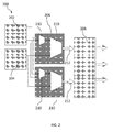
- the modules 118 may be configured using multiplexers placed between them.
- a first module 202 having three output ports and a second module 204 having one output port are connected via a system of multiplexers 206 to a third module 208 having two input ports (and three output ports).
- the third module 208 may receive any of the outputs of the first 202 and second 204 modules as either of its two inputs 212.
- the select lines 210 may be configured via processor or DMA control, in a manner similar to the configuration of other module parameters.
- One of skill in the art will understand that other configurations for the multiplexers 206 are also within the scope of the invention.
- Any given module may be moved across the camera pipe and/or memory pipe as part of the pipe reconfiguration.
- the camera pipes may work on the pixel clock and the memory pipe may work on the system clock; both clocks may be asynchronous with respect to each other.
- the PVP architecture may ensure proper synchronization across clock domains so that a module may be switched between the pipes.
- the image-processing modules in the PVP may be accessed by a linked processor via, for example, memory-mapped registers ("MMRs") accessible via an APB interface (such as the interface 134 shown in FIG. 1 ).
- MMRs memory-mapped registers
- APB interface such as the interface 134 shown in FIG. 1
- a hardware interrupt may be asserted, for example, and the processor may read and write status and control information to and from the PVP and its modules.
- the flow of image data may be dictated either by the processor or by a DMA engine.
- the image-processing modules may be configured by either or both of the APB interface (i.e., via the processor) and one or more DMA interfaces.
- all of the processing modules are controlled at a first point in time by direct processor control and, at a second point in time, by DMA control.
- a first subset of the modules is configurable by direct processor control while, simultaneously, a second subset is configurable by DMA control.
- the first subset of modules may be modules that process data stored in a memory (i.e., a memory pipe) and the second subset may be modules that process data coming from a camera sensor (i.e., a camera pipe).
- a first DMA control channel may control the first subset of modules and a second DMA control channel may control the second subset of modules.
- the first DMA control channel controls the camera pipe and the second controls the memory pipe.
- One of skill in the art will understand that other combinations of read and write control are possible and that the current invention is not limited to any particular division of direct and DMA control.
- direct or DMA control of the registers is accomplished by reading or writing first to a set of scratch registers; once these scratch registers are fully written, for example, their contents are then applied to the actual application registers. Likewise, reading of the control registers may first fill one or more scratch registers, and then the scratch registers are read via DMA control.
- the scratch registers may be the shadow registers 130, 132 shown in FIG. 1 .
- direct processor control by the APB interface is not allowed during loading or unloading of the shadow registers (i.e., during the time the contents of the shadow registers are being applied to the application registers or during the time the status registers are filling the shadow registers).
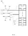
- FIG. 3A illustrates an illustrative arbitration scheme 300 in accordance with an embodiment of the invention.
- a first DMA channel 302 is used to configure modules in a camera pipeline; modules in a memory pipeline may be configured using either a second DMA channel 304 or an APB link 306 for direct control by a processor.
- An arbitration unit 308 is used to resolve conflicts between the second DMA channel 304 and the APB link 306.
- the arbitration unit 308 may include a stall or blackout mechanism to delay access to the DMA engine during some or all of its loading phase and/or error signaling to thereby safeguard the validity of any simultaneous accesses by the APB link 306.
- the arbitration module 308 interfaces with the DMA engine 304 and the APB link 306 and controls how the control data is programmed/arbitrated to the image-processing modules.
- the arbitration module 308 is incorporated into the image-pipe controller ("IPC") 140, shown in FIG. 1 , and communicates with the DMA engine and processor via P2P and APB buses, respectively.
- the image-processing modules may use an internal bus, such as an AHB bus.
- FIG. 3B One embodiment of an implementation of the arbitration logic is shown in FIG. 3B .
- the clock controlling some or all of the image-processing modules may be on a different domain than that of the clock domain of the DMA and processor interfaces. In this case, the clocks may be synchronized across the different domains.
- subsets of the image-processing modules are arranged in a plurality of different-length pipes, and data may finish processing in a shorter pipe (and, e.g., assert a load_done signal to indicate completion) before it finishes processing in a longer pipe.
- a synchronization module 310 may delay synchronization of the early data until the later data is also available by, for example, receiving a load_done signal from each of the pipelines and sending a synchronization signal to the arbitration unit 308 when some or all of the load_done signals have been received.
- DMA status channels may be used to scan out one or more values in the parameter registers. For example, a histogram status may be scanned out, from the THC module, on the DMA status channel.
- the trigger of the DMA status channel may be based on a vsync output at a given module. If two statuses are requested over the same channel, an identifying field (e.g., numbers or letters) may be included in a status header for each module's status, and the two statuses may be sequenced, one after the other, after recording the event.
- a special control-word format called a block-control structure list (“BCL") may be defined in a system memory.
- the BCL is an array of control information intended for the application registers in the image-processing modules in the PVP; this control information is grouped by module, and each group contains header information (e.g., a block-control header or "BCH”) instructing the PVP where and how to apply the control information.
- the BCL is read in via DMA, the header information is decoded by the image-pipe controller, and the control information is thereby applied to the modules.
- the structure of the BCL may allow a new module to be added easily by, e.g., appending or inserting a new module's BCH in the BCL.
- FIG. 4 illustrates one embodiment of a BCL 400.
- a number of BCHs 402 are shown, each having an associated list of block-control words 404.
- FIG. 5 illustrates an expanded view of a BCH 500.
- a first field BLOCK 502 indicates a unique address assigned to each image-processing module in the PVP, and thereby instructs the image-pipe controller to which module to apply the parameters.
- a second field WCNT 504 indicates the number of control words contained in this block, thereby indicating the location of the next BCH. The use of the WCNT field may obviate the need for, for example, an end-of-block indicating field at the end of the block.
- WOFF 506 indicates an offset to be applied to the control words; for example, if a given module has a set of 256 registers, specifying an offset of 10 means that the control words are applied beginning at the tenth register. If WCNT is 12 (for example), registers 10 through 22 are programmed.
- IPORT fields 508 may be used to select a first level of multiplexers
- IBLOCK fields 510 may be used to select a second level of multiplexers.
- select bits are within the scope of the current invention.
- all the IBLOCK(s) and IPORT(s) may be removed from the BCH and a separate crossbar-control header format (i.e., a crossbar-control structure or "CCS" packet) may be defined.
- CCS crossbar-control structure
- START bit 512 indicates whether a module should be enabled or disabled
- PIPE field 514 indicates to which pipe a module should belong (i.e., a camera or memory pipe).
- STATWCNT 516 indicates how many status registers in a module should be read out in a read operation.
- a BCL for a given pipe begins with a configuration of an input-data format module, includes configuration of one or more image-processing modules, and ends with a configuration of an output-data format module.
- the order of the configuration information for each image-processing module may correspond to the positions of the modules in the pipe.
- the BCH for a module may be repeated within a BCL (e.g., two or more times) to allow programming of two separate groups of registers for a given module inside a pipe. For example, a first BCH may be used to program registers 10-22 of a module, and a second BCH may be used to program registers 100-110 of the same module.
- the configuration of the BCH for a given module may correlate to the direct processor control of the module via memory-mapped registers.
- a given module may have a fixed base address for access via the processor; the BLOCK 502 identification number of the module (used for DMA control) may be derived from this base address.
- the BLOCK 502 identification may be found by right-shifting the base address by five bits.
- the difference between an actual MMR address and the base address may correlate directly to the WOFF offset field in the BCH.
- each control word in the BCL is arranged in the same order that they appear in the MMR address space, thereby simplifying the design of the BCH and of any software that configures the registers in the modules using either control scheme.
- a programmer and/or software utility may seamlessly shift between the two control schemes without the use of, for example, a decoder/mapping utility to translate between the schemes.
- Reading status via DMA is performed in a manner similar to writing control information through DMA.
- module status values are moved into one or more shadow registers in accordance with the output capabilities of a given module (i.e., according to the clock rate of the module).
- the status information is then periodically sent via DMA in accordance with configuration registers (e.g., once every frame boundary or once every certain number of frames).
- the status information may be sent on a single DMA channel or simultaneously over multiple DMA channels.
- a STATWCNT field 516 in the BCH indicates the number of status registers in a module to be read and sent.
- embodiments of the present invention allow seamless reprogramming of parameter registers for modules comprising of any given pipe, such that back-to-back frames may be processed with different coefficients or variations of the algorithm provided by each module.
- a given module may have a latency of more than one clock cycle; the pipeline stages at the end of the module may, for example, be processing a first frame while the pipeline stages at the beginning of the module may be processing a second frame.
- the application registers that influence the behavior of the module may thus be updated at different times for each pipeline of the module to ensure that each frame is processed in accordance with its intended parameters.
- the application registers in each pipeline are updated as a frame boundary propagates through the pipeline in the module.
- shadow registers may be used to update the application registers at the appropriate times; either the direct-processor MMR mechanism or the DMA control mechanism updates the shadow registers only, and the updating of the application registers is staggered in time.
- the engine may control the granularity at which a given set of parameters or a given configuration is applied: continuously for every frame or for a fixed set of frames.
- the camera pipe continuously gets frames from the camera sensor, while the memory pipe receives fixed sets of frames; either mode may be used with either pipe, however.
- the processor may be switched from continuous mode to fixed mode (and vice versa) without disabling the entire PVP engine.
- a flag may be set (e.g., a frame count or "FCNT" value may be programmed to zero). If a new set of control values are programmed, the new values are be applied on the next frame boundary and applied to subsequent frames continuously thereafter.
- the architecture may also provide a TAG mechanism on a separate status DMA channel for ease of identification of the frames which have been processed with new control parameters; the processor may use this TAG mechanism to determine which frames received processing using a certain set of parameters.
- the TAG data may be sent on the status DMA channel and may also be available for processor read.
- the FCNT value may be programmed to a nonzero value and thereafter monitored. Once the predetermined number of frames has been processed, the pipeline halts (and the last frame is stuck in the pipeline). Once a next group of frames is identified and queued for processing, the FCNT value is set again, and the next group begins processing (with, perhaps, a different set of module parameters). Processing of the next group of frames pushes out the last frame of the previous set that was stuck in the pipeline.
- the pipeline may be flushed if another parameter (e.g., a DRAIN bit) is set. If, for example, a finite set of frames is identified for processing and the DRAIN bit is set, upon completion of the last frame, the pipeline is flushed with dummy pixels so that the last frame in the set is output by the pipeline. As the last frame passes through the pipeline, the modules in the pipeline are disabled. In one embodiment, if the pipeline is in a continuous-frame mode and the DRAIN bit is set, the pipeline is immediately flushed and disabled. In either case, the next set of control words may be set to wake up the pipeline (by use of, for example, a START bit in the BCH of the frames).
- a DRAIN bit e.g., a DRAIN bit
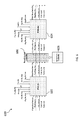
- FIG. 6 illustrates an exemplary embodiment 600 of a first module 602, a second module 604, a data control and crossbar unit 606 connecting them, and an image-pipe controller 608.
- a "daisychainload" signal is driven together with a frame sync signal to the first module 602.
- the first module 602 updates its application registers in accordance with its internal pipeline delays as the first pixel in the input data passes through the module 602 (i.e., if the first module includes five pipeline stages, it applies the application-register values in turn to each of the five stages as the pixel data is processed through).
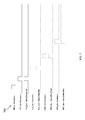
- FIG. 7 A timing diagram 700 of the daisychainload signal and the frame sync signal is shown in FIG. 7
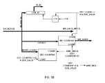
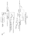
- FIG. 8 illustrates a logic circuit 800 for gating the clocks and generating block reset based on a drain_done and start bit.
- the pipelines themselves may be reconfigured by adding or deleting modules.
- the engine may include a mechanism that permits a seamless, dynamic reconfiguration of the modules comprising the camera pipes with a loss of one frame data only.
- the engine may include a mechanism that permits dynamic reconfiguration with a finite stall and no frame loss.
- FIG. 9 illustrates an exemplary embodiment 900 of a PVP architecture.
- the system includes a camera input 902 and a memory input 904.
- the camera input 902 feeds three camera pipelines 906, 908, 910, and the memory input 904 feeds two memory pipelines 912, 914.
- the first camera pipeline 906 includes two convolution/down-scaler modules, a pixel-magnitude and angle computation module, and a pixel-edge classifier module;
- the second camera pipeline 908 includes a convolution/down-scaler module and an integral image computation module;
- the third camera pipeline 910 contains a threshold, histogram, and compression module;
- the first memory pipeline 912 includes a convolution/down-scaler module and an arithmetic computation unit; and the second memory pipeline includes an up-down scaler.
- FIG. 10 illustrates a system 1000 including a PVP 1002 and its support and interface circuitry.
- a processor 1004 may directly control the PVP 1002 via an MMR interface.
- a VSS crossbar circuit 1006 provides data to the camera pipeline; the crossbar 1006 may select between a variety of input sources (e.g., PPI and PIXC inputs), thereby providing multiple camera inputs.
- DDE arbitration units 1008 interface with external buses (e.g., AXI buses) to allow for DMA control; DDE units 1010 off-load output data from the output-data format modules within the PVP 1002, provide input and output control and status data, and provide an input to the memory pipeline.
Landscapes
- Engineering & Computer Science (AREA)
- Physics & Mathematics (AREA)
- General Physics & Mathematics (AREA)
- Theoretical Computer Science (AREA)
- Multimedia (AREA)
- Signal Processing (AREA)
- Image Processing (AREA)
- Compression Or Coding Systems Of Tv Signals (AREA)
- Advance Control (AREA)
- Stored Programmes (AREA)
- Bus Control (AREA)
- Microcomputers (AREA)
- Television Signal Processing For Recording (AREA)
- Multi Processors (AREA)
- Cash Registers Or Receiving Machines (AREA)
- Information Transfer Systems (AREA)
- Studio Devices (AREA)
Abstract
Description
- This application claims priority to
U.S. Provisional Patent Application No. 61/547,442, filed on October 14, 2011 - A stream of video frames, such as that generated by a video camera or read from a memory, frequently requires processing to improve the quality of the video or to extract features from the video. This processing is traditionally done by software in a post-processing operation. The post-processing operation may vary because (i) the parameters/coefficients of the algorithmic processing modules need to be modified; (ii) fine variations of a given algorithm need to be performed; and/or (iii) the operations that need to be performed on the video need to be changed. A software solution, however, while versatile, is slow and expensive in terms of processing power. Hardware-based algorithms are typically faster and more efficient, but hardware, by its nature, is difficult to reconfigure quickly and easily, especially when it must keep pace with live, streaming video. Existing hardware-based image processing systems thus produce non-optimal results because of their limitations in flexibility. A need therefore exists for a fast, efficient, and reconfigurable hardware-based image-processing system.
- In one embodiment of the current invention, a pipelined video pre-processor ("PVP") is made up of several algorithmic transformation image-processing modules that may be connected to each other in a variety of different, customizable configurations. Each of these modules has a plurality of parameter registers that control finite variations of a given algorithm implementation. The parameters of the modules may be re-configured on a frame-by-frame basis with no loss of data, and the configuration of modules may be changed with minimal or no loss of data. The parameters may be changed via a connected processor, via DMA access, or both simultaneously. The differing control schemes are designed to be compatible with each other, ensuring seamless transitions between them.
- In one aspect, a pipelined video pre-processor includes a plurality of image-processing modules arranged in a pipeline. An input port receives configuration parameters for the plurality of modules, and an image-pipe controller decodes the configuration parameters. A shadow register applies the configuration parameters to the plurality of modules, thereby altering the image-processing characteristics of the modules.
- The pipeline may be a memory pipeline for processing image data from a memory or a camera pipeline for processing image data from a digital camera. One or more additional pipelines (e.g., memory pipelines or camera pipelines) may be included. The configuration parameters may be received from a processor or a direct-memory access ("DMA") engine. The configuration parameters may be arranged in a memory in a block-control structure and are accessed via a DMA channel; the block-control structure may include a block-control header and one or more block-control words. The offsets of the block-control words in the block-control structure may correspond to addresses in a memory-mapped register ("MMR") space. The configuration parameters may be applied to a first frame of video data, and updated configuration parameters may be applied to a second frame of video data. Different pipeline stages in a module may receive the updated configuration parameters at different points in time in accordance with a data boundary.
- In another aspect, a method of processing image frames in a pipelined video pre-processor includes receiving configuration parameters for a plurality of image-processing modules in the pipelined video pre-processor. The configuration parameters may be stored in a shadow register and applied to the plurality of image-processing modules to thereby alter the image-processing characteristics of the modules.
- The configuration parameters may be received from a processor or a DMA engine; the modules may be arranged in one or more pipelines. The one or more pipelines may include a memory pipeline for processing image data from a memory or a camera pipeline for processing image data from a digital camera. The configuration parameters may be arranged in a memory in a block-control structure and may be accessed via a DMA channel. The block-control structure may include a block-control header and one or more block-control words. The offsets of the block-control words in the block-control structure may correspond to addresses in a memory-mapped register ("MMR") space. The configuration parameters may be applied to a first frame of video data and updated configuration parameters may be applied to a second frame of video data. Different pipeline stages in a module may receive the updated configuration parameters at different points in time in accordance with a data boundary.
- In another aspect, a pipelined video pre-processor in a digital-signal processor includes a plurality of image-processing modules arranged in a pipeline and an input port for receiving configuration parameters for the plurality of modules. An image-pipe controller decodes the configuration parameters, and a shadow register applies the configuration parameters to the plurality of modules, thereby altering the image-processing characteristics of the modules. The pipeline may be a memory pipeline for processing image data from a memory or a camera pipeline for processing image data from a digital camera.
- In another aspect, a system for configuring modules in a pipelined pre-processor includes a first input port for receiving a first control signal from a processor and a second input port for receiving a second control signal from a memory. An arbitration unit resolves a conflict between the first and second control signals. A controller decodes the first and second control signals and applies configuration parameters derived therefrom to the modules.
- An interface (e.g., an advanced peripheral bus ("APB") interface) may be used to decode the first control input. The first control signal may be a memory-mapped register ("MMR") input, and the second control signal may be received from one or more direct-memory access ("DMA") channels. The first control signal may control a first subset of the modules and, simultaneously, the second control input may control a second subset of the modules. A module may be controlled by both the first and second control signals. A shadow register may receive one of the decoded first and second control signals. The shadow register may writes an application register in at least one module to thereby apply the configuration parameters to the module. The arbitration unit may stall the second control signal in the event of a conflict.
- In another aspect, a method for configuring modules in a pipelined pre-processor includes receiving a first control signal from a processor and a second control signal from a memory. A conflict is resolved between the first and second control signals. The first and second control signals are decoded, and configuration parameters derived therefrom are applied to the modules.
- A shadow register may be filled with information derived from one of the first or second control signals. A module may be configured in accordance with the contents of the shadow register. The first control signal may be ignored during configuring of the module. The second control signal may be stalled in the event of a conflict. The second control signal may be received from one or more DMA channels. The first control signal may control a first subset of the modules and, simultaneously, the second control input may control a second subset of the modules. A module may be controlled by both the first and second control signals.
- In another aspect, a pipelined video pre-processor having configurable modules in a digital-signal processor includes a first input port for receiving a first control signal from the digital-signal processor and a second input port for receiving a second control signal from a memory. An arbitration unit resolves a conflict between the first and second control signals. A controller decodes the first and second control signals and configuration parameters derived therefrom are applied to the modules. The first control signal may be an MMR input and the second control signal may be a DMA input.
- In another aspect, a system for programming reconfigurable modules in a pipelined video pre-processor includes an input port for receiving a block-control structure from a memory via a direct-memory access ("DMA") channel. An image-pipe controller decodes a block-control header in the block-control structure and selects a block-control word in the block-control structure in accordance with the decoded block-control header. A shadow register receives the block-control word and applies parameters in the block-control word to an application register in a reconfigurable module, thereby adjusting a parameter of the module.
- The block-control header may include a block address that uniquely identifies the module. The input port may further receive a block-control list comprising a plurality of block-control structures. The block-control header may include a word count that comprises a number of block-control structures. An order of the block-control structures may correspond to an order of modules in a pipeline. The block-control header may include an offset indicating which application register receives the block-control word. The offset may be equivalent to the difference between an memory-mapped register ("MMR") address of an application register in the module and an MMR base address of the module. The block-control header may include multiplexer-select information for specifying how the module connects to a second module. An offset of a block-control word intended for an application register may correspond to an address of the same application register in a memory-mapped register ("MMR") space. The offset of the block-control word may be obtained by shifting the address.
- In another aspect, a method for programming reconfigurable modules in a pipelined video pre-processor includes receiving a block-control structure from a memory via a direct-memory access ("DMA") channel and decoding a block-control header in the block-control structure. A block-control word in the block-control structure is selected in accordance with the decoded block-control header. Parameters in the block-control word are applied to an application register in a reconfigurable module, thereby adjusting a parameter of the module.
- Decoding the block-control header may include decoding a block address that uniquely identifies the module. A block-control list comprising a plurality of block-control structures may be received. Decoding the block-control header may include decoding a word count that comprises a number of block-control structures. Block-control words in each of the block-control structures may be applied to each of a plurality of modules. An order of the block-control structures may correspond to an order of the modules in a pipe. Parameters in the block-control word may be applied to a multiplexer select to thereby configure a connection between two modules. A status register may be read from a module in accordance with a status count in the block-control header.
- In another aspect, a pipelined video pre-processor having a plurality of reconfigurable modules in a digital-signal processor includes an input port for receiving a block-control structure from a memory via a direct-memory access ("DMA") channel. An image-pipe controller decodes a block-control header in the block-control structure and selects a block-control word in the block-control structure in accordance with the decoded block-control header. A shadow register receives the block-control word and applies parameters in the block-control word to an application register in a reconfigurable module, thereby adjusting a parameter of the module. An offset of a block-control word intended for an application register may correspond to an address of the same application register in a memory-mapped register ("MMR") space.
- In another aspect, a system for programming reconfigurable modules in a pipelined video pre-processor includes a reconfigurable hardware module for processing image data. A shadow register stores an updated set of module parameters. An image-pipe controller applies the updated set of parameters to the module. An application register within the module receives the updated set of parameters. Different pipeline stages in the module receive the updated set of parameters at different times in accordance with the propagation of a data boundary through the pipeline.
- The updated set of module parameters may be received from one of a processor or a direct-memory access ("DMA") channel. The image data may include image frames and the data boundary is a frame boundary. The updated set of module parameters may be applied to one of a continuous series of image frames or to a fixed number of image frames. Image data processed using the updated set of module parameters may be tagged accordingly; the tagged information may be output using a DMA channel or a processor output. The pipeline may be flushed in accordance with a drain command. A connection between the module and a second module may be altered when the pipeline is flushed. The module may assert a control signal when the updated set of parameters has been applied to every stage in its pipeline. A downstream module may begin applying the updated set of parameters upon assertion of the control signal.
- In another aspect, a method for programming reconfigurable modules in a pipelined video pre-processor includes receiving, in a shadow register, an updated set of parameters for a module for processing image data. The updated set of parameters is sent to the module. The updated set of parameters is sent to different pipeline stages in the module at different points in time in accordance with the propagation of a data boundary through the pipeline.
- The image data may include image frames and the data boundary may be a frame boundary. The updated set of module parameters may be applied to one of a continuous series of image frames or to a fixed number of image frames. Image data processed using the updated set of module parameters may be tagged, and the tagged image data may be output using a DMA channel or a processor output. The pipeline may be flushed in accordance with a drain command; a connection between the module and a second module may be altered when the pipeline is flushed.
- In another aspect, a pipelined video pre-processor system having a plurality of reconfigurable modules in a digital-signal processor includes a reconfigurable hardware module for processing image data. A shadow register stores an updated set of module parameters. An image-pipe controller applies the updated set of parameters to the module. An application register within the module receives the updated set of parameters. Different pipeline stages in the module receive the updated set of parameters at different times in accordance with the propagation of a data boundary through the pipeline. The updated set of module parameters may be received from one of the digital-signal processor or a direct-memory access ("DMA") channel. The image data may include image frames and the data boundary may be a frame boundary.
- These and other objects, along with advantages and features of the present invention herein disclosed, will become more apparent through reference to the following description, the accompanying drawings, and the claims. Furthermore, it is to be understood that the features of the various embodiments described herein are not mutually exclusive and can exist in various combinations and permutations.
- In the drawings, like reference characters generally refer to the same parts throughout the different views. In the following description, various embodiments of the present invention are described with reference to the following drawings, in which:
-
FIG. 1 is a block diagram of a PVP in accordance with an embodiment of the present invention; -
FIG. 2 is a block diagram of module configuration in accordance with an embodiment of the present invention; -
FIGS. 3A and3B are implementations of an arbitration scheme in accordance with an embodiment of the present invention; -
FIG. 4 is an illustration of a block-control list in accordance with an embodiment of the present invention; -
FIG. 5 is an illustration of a block-control header in accordance with an embodiment of the present invention; -
FIG. 6 is a block diagram of a frame-by-frame parameter update scheme in accordance with an embodiment of the present invention; -
FIG. 7 is a timing diagram of frame-by-frame updating in accordance with an embodiment of the present invention; -
FIG. 8 alogic circuit 800 for gating the clocks and generating block reset in accordance with an embodiment of the present invention; -
FIG. 9 is an exemplary PVP in accordance with an embodiment of the present invention; and -
FIG. 10 is block diagram of a system incorporating a PVP in accordance with an embodiment of the present invention. -
FIG. 1 illustrates an embodiment of a pipelined video pre-processor ("PVP") 100. The PVP may operate on any incoming data; in one embodiment, the data is video image data captured from a camera sensor and/or video image data fetched from a memory. The PVP may be placed on a stand-alone silicon chip; in other embodiments, the PVP is placed on a chip along with a processor, such as a digital-signal processor. A first input-data formatter 102 may be used to formatincoming camera data 104 from a camera source, and a second input-data formatter 106 may be used to formatmemory data 108 from a memory source. Data from one or more sources may be processed simultaneously. The present invention is not limited to any particular number or kind of input sources, and the input data sources may include one ormore camera sources 104 and/or one ormore memory sources 108. Eachsource data formatter data formatters other sources - The input-
data formatters reconfigurable pipelines pipeline more processing modules 118. As explained in greater detail below, theprocessing modules 118 perform a variety of different image-processing functions and tasks and may be selected and configured in accordance with a desired image-processing result. The number ofmodules 118 per pipeline, the order of themodules 118 within the pipeline, and the configuration of themodules 118 within a pipeline may be reconfigured as necessary, and a givenmodule 118 may be selected for use indifferent pipelines FIG. 1 illustrates fourmodules 118 in the first pipeline 110 (twomodules 118 being configured to operate in parallel), twomodules 118 in thesecond pipeline 112, onemodule 118 in thethird pipeline 114, and twomodules 118 in thefourth pipeline 116. This configuration of modules is presented as only one possible configuration of thePVP 100, however, and one of skill in the art will understand that many other configurations are possible. - The outputs of the
pipelines data formatters output ports 128. In one embodiment, the output-data formatters pipeline data formatter more pipelines - Each
module 118 may have internal configuration parameters that are controlled by an outside source. Eachmodule 118 may have its own set of local parameter registers that determine the nature of processing offered by that module within the confines of a given algorithm; additional parameter registers may be common to some or all of themodules 118. The parameter registers may include application registers 130 and/or status registers 132; only one set of these registers is shown for illustrative purposes, but eachmodule 118 may contain its own set ofapplication 130 andstatus 132 registers. As explained in greater detail below, the parameter registers may be read or written by a variety of sources, including a connected processor (via aninterface 134, such as an advanced peripheral bus or "APB" interface) or via direct-memory access ("DMA") though the use of input andoutput modules 136. In one embodiment, control and status information is input and output via the use of shadow registers 138; the shadow registers 138 read and write to the application registers 130 and/or status registers 132 in accordance with the timing of image data currently moving through apipeline pipe controller 140 may be used to coordinate control of themodules 118, as explained in greater detail below. - In various embodiments, the
modules 118 may include a convolution/down-scaler engine ("CNV"); a pixel-magnitude and angle-computation unit ("PMA"); a threshold, histogram and compression engine ("THC"); an arithmetic computation unit ("ACU"); a pixel-edge classifier ("PEC"); an integral image computation ("IIM"); and/or an up-down scaler ("UDS"). One of skill in the art will understand that other modules may be included and that the present invention is not limited to only these modules. Themodules 118 may be selectively connected to each other to create one or more different pipelines using any method known in the art such as, e.g., a programmable crossbar switch. In one embodiment, illustrated inFIG. 2 , themodules 118 may be configured using multiplexers placed between them. In thesystem 200 shown inFIG. 2 , afirst module 202 having three output ports and asecond module 204 having one output port are connected via a system ofmultiplexers 206 to athird module 208 having two input ports (and three output ports). By controlling theselect lines 210 of themultiplexers 206, thethird module 208 may receive any of the outputs of the first 202 and second 204 modules as either of its twoinputs 212. Theselect lines 210 may be configured via processor or DMA control, in a manner similar to the configuration of other module parameters. One of skill in the art will understand that other configurations for themultiplexers 206 are also within the scope of the invention. - Any given module may be moved across the camera pipe and/or memory pipe as part of the pipe reconfiguration. The camera pipes may work on the pixel clock and the memory pipe may work on the system clock; both clocks may be asynchronous with respect to each other. The PVP architecture may ensure proper synchronization across clock domains so that a module may be switched between the pipes.
- In one embodiment, the image-processing modules in the PVP may be accessed by a linked processor via, for example, memory-mapped registers ("MMRs") accessible via an APB interface (such as the
interface 134 shown inFIG. 1 ). A hardware interrupt may be asserted, for example, and the processor may read and write status and control information to and from the PVP and its modules. Once the processing modules are appropriately configured, the flow of image data may be dictated either by the processor or by a DMA engine. - In another embodiment, the image-processing modules may be configured by either or both of the APB interface (i.e., via the processor) and one or more DMA interfaces. In one embodiment, all of the processing modules are controlled at a first point in time by direct processor control and, at a second point in time, by DMA control. In another embodiment, a first subset of the modules is configurable by direct processor control while, simultaneously, a second subset is configurable by DMA control. For example, in the PVP, the first subset of modules may be modules that process data stored in a memory (i.e., a memory pipe) and the second subset may be modules that process data coming from a camera sensor (i.e., a camera pipe). In another embodiment, there may be a plurality (e.g., two or more) separate DMA control channels. A first DMA control channel may control the first subset of modules and a second DMA control channel may control the second subset of modules. For example, the first DMA control channel controls the camera pipe and the second controls the memory pipe. One of skill in the art will understand that other combinations of read and write control are possible and that the current invention is not limited to any particular division of direct and DMA control.
- In one embodiment, direct or DMA control of the registers is accomplished by reading or writing first to a set of scratch registers; once these scratch registers are fully written, for example, their contents are then applied to the actual application registers. Likewise, reading of the control registers may first fill one or more scratch registers, and then the scratch registers are read via DMA control. The scratch registers may be the shadow registers 130, 132 shown in
FIG. 1 . In one embodiment, direct processor control by the APB interface is not allowed during loading or unloading of the shadow registers (i.e., during the time the contents of the shadow registers are being applied to the application registers or during the time the status registers are filling the shadow registers). - Because control of the modules may come from different sources, conflicts may arise between multiple simultaneous requests. In one embodiment, arbitration may be used to resolve conflicts between the different control mechanisms.
FIG. 3A illustrates anillustrative arbitration scheme 300 in accordance with an embodiment of the invention. In this embodiment, afirst DMA channel 302 is used to configure modules in a camera pipeline; modules in a memory pipeline may be configured using either asecond DMA channel 304 or anAPB link 306 for direct control by a processor. Anarbitration unit 308 is used to resolve conflicts between thesecond DMA channel 304 and theAPB link 306. Thearbitration unit 308 may include a stall or blackout mechanism to delay access to the DMA engine during some or all of its loading phase and/or error signaling to thereby safeguard the validity of any simultaneous accesses by theAPB link 306. In one embodiment, thearbitration module 308 interfaces with theDMA engine 304 and theAPB link 306 and controls how the control data is programmed/arbitrated to the image-processing modules. In one embodiment, thearbitration module 308 is incorporated into the image-pipe controller ("IPC") 140, shown inFIG. 1 , and communicates with the DMA engine and processor via P2P and APB buses, respectively. The image-processing modules may use an internal bus, such as an AHB bus. One embodiment of an implementation of the arbitration logic is shown inFIG. 3B . - The clock controlling some or all of the image-processing modules may be on a different domain than that of the clock domain of the DMA and processor interfaces. In this case, the clocks may be synchronized across the different domains. In one embodiment, subsets of the image-processing modules are arranged in a plurality of different-length pipes, and data may finish processing in a shorter pipe (and, e.g., assert a load_done signal to indicate completion) before it finishes processing in a longer pipe. A
synchronization module 310 may delay synchronization of the early data until the later data is also available by, for example, receiving a load_done signal from each of the pipelines and sending a synchronization signal to thearbitration unit 308 when some or all of the load_done signals have been received. - The bits of the parameter registers may be set or cleared by the processor using polling or interrupts. In one embodiment, DMA status channels may be used to scan out one or more values in the parameter registers. For example, a histogram status may be scanned out, from the THC module, on the DMA status channel. The trigger of the DMA status channel may be based on a vsync output at a given module. If two statuses are requested over the same channel, an identifying field (e.g., numbers or letters) may be included in a status header for each module's status, and the two statuses may be sequenced, one after the other, after recording the event.
- To facilitate control through DMA, a special control-word format called a block-control structure list ("BCL") may be defined in a system memory. The BCL is an array of control information intended for the application registers in the image-processing modules in the PVP; this control information is grouped by module, and each group contains header information (e.g., a block-control header or "BCH") instructing the PVP where and how to apply the control information. The BCL is read in via DMA, the header information is decoded by the image-pipe controller, and the control information is thereby applied to the modules. The structure of the BCL may allow a new module to be added easily by, e.g., appending or inserting a new module's BCH in the BCL.
-
FIG. 4 illustrates one embodiment of aBCL 400. A number ofBCHs 402 are shown, each having an associated list of block-control words 404.FIG. 5 illustrates an expanded view of aBCH 500. Afirst field BLOCK 502 indicates a unique address assigned to each image-processing module in the PVP, and thereby instructs the image-pipe controller to which module to apply the parameters. Asecond field WCNT 504 indicates the number of control words contained in this block, thereby indicating the location of the next BCH. The use of the WCNT field may obviate the need for, for example, an end-of-block indicating field at the end of the block. Another field,WOFF 506, indicates an offset to be applied to the control words; for example, if a given module has a set of 256 registers, specifying an offset of 10 means that the control words are applied beginning at the tenth register. If WCNT is 12 (for example), registers 10 through 22 are programmed. - Further fields in the BCH indicate how a module should be connected to upstream and downstream modules using, for example, the multiplexer control illustrated in
FIG. 2 . For example, IPORT fields 508 may be used to select a first level of multiplexers, andIBLOCK fields 510 may be used to select a second level of multiplexers. One of skill in the art will understand, however, that any other method of specifying multiplexer programming using select bits is within the scope of the current invention. Alternatively, all the IBLOCK(s) and IPORT(s) may be removed from the BCH and a separate crossbar-control header format (i.e., a crossbar-control structure or "CCS" packet) may be defined. Other fields include aSTART bit 512 that indicates whether a module should be enabled or disabled and aPIPE field 514 that indicates to which pipe a module should belong (i.e., a camera or memory pipe). Another field,STATWCNT 516, indicates how many status registers in a module should be read out in a read operation. - In one embodiment, a BCL for a given pipe begins with a configuration of an input-data format module, includes configuration of one or more image-processing modules, and ends with a configuration of an output-data format module. The order of the configuration information for each image-processing module may correspond to the positions of the modules in the pipe. The BCH for a module may be repeated within a BCL (e.g., two or more times) to allow programming of two separate groups of registers for a given module inside a pipe. For example, a first BCH may be used to program registers 10-22 of a module, and a second BCH may be used to program registers 100-110 of the same module.
- The configuration of the BCH for a given module may correlate to the direct processor control of the module via memory-mapped registers. For example, a given module may have a fixed base address for access via the processor; the
BLOCK 502 identification number of the module (used for DMA control) may be derived from this base address. In one embodiment, theBLOCK 502 identification may be found by right-shifting the base address by five bits. Similarly, the difference between an actual MMR address and the base address may correlate directly to the WOFF offset field in the BCH. Thus, each control word in the BCL is arranged in the same order that they appear in the MMR address space, thereby simplifying the design of the BCH and of any software that configures the registers in the modules using either control scheme. For example, if a given register is 36 address units removed from the base address in the MMR address space, that same register is 36 units offset from theBLOCK 502 identification number in the DMA control scheme. Using this configuration, a programmer and/or software utility may seamlessly shift between the two control schemes without the use of, for example, a decoder/mapping utility to translate between the schemes. - Reading status via DMA is performed in a manner similar to writing control information through DMA. In one embodiment, module status values are moved into one or more shadow registers in accordance with the output capabilities of a given module (i.e., according to the clock rate of the module). The status information is then periodically sent via DMA in accordance with configuration registers (e.g., once every frame boundary or once every certain number of frames). The status information may be sent on a single DMA channel or simultaneously over multiple DMA channels. As explained above, a
STATWCNT field 516 in the BCH indicates the number of status registers in a module to be read and sent. - For a given pipe configuration, embodiments of the present invention allow seamless reprogramming of parameter registers for modules comprising of any given pipe, such that back-to-back frames may be processed with different coefficients or variations of the algorithm provided by each module. A given module may have a latency of more than one clock cycle; the pipeline stages at the end of the module may, for example, be processing a first frame while the pipeline stages at the beginning of the module may be processing a second frame. The application registers that influence the behavior of the module may thus be updated at different times for each pipeline of the module to ensure that each frame is processed in accordance with its intended parameters. In one embodiment, the application registers in each pipeline are updated as a frame boundary propagates through the pipeline in the module. As described above, shadow registers may be used to update the application registers at the appropriate times; either the direct-processor MMR mechanism or the DMA control mechanism updates the shadow registers only, and the updating of the application registers is staggered in time.
- The engine may control the granularity at which a given set of parameters or a given configuration is applied: continuously for every frame or for a fixed set of frames. Typically, the camera pipe continuously gets frames from the camera sensor, while the memory pipe receives fixed sets of frames; either mode may be used with either pipe, however. The processor may be switched from continuous mode to fixed mode (and vice versa) without disabling the entire PVP engine. To apply the parameters to every frame, a flag may be set (e.g., a frame count or "FCNT" value may be programmed to zero). If a new set of control values are programmed, the new values are be applied on the next frame boundary and applied to subsequent frames continuously thereafter. The architecture may also provide a TAG mechanism on a separate status DMA channel for ease of identification of the frames which have been processed with new control parameters; the processor may use this TAG mechanism to determine which frames received processing using a certain set of parameters. The TAG data may be sent on the status DMA channel and may also be available for processor read.
- To apply the parameters to a fixed set of frames, the FCNT value may be programmed to a nonzero value and thereafter monitored. Once the predetermined number of frames has been processed, the pipeline halts (and the last frame is stuck in the pipeline). Once a next group of frames is identified and queued for processing, the FCNT value is set again, and the next group begins processing (with, perhaps, a different set of module parameters). Processing of the next group of frames pushes out the last frame of the previous set that was stuck in the pipeline.
- The pipeline may be flushed if another parameter (e.g., a DRAIN bit) is set. If, for example, a finite set of frames is identified for processing and the DRAIN bit is set, upon completion of the last frame, the pipeline is flushed with dummy pixels so that the last frame in the set is output by the pipeline. As the last frame passes through the pipeline, the modules in the pipeline are disabled. In one embodiment, if the pipeline is in a continuous-frame mode and the DRAIN bit is set, the pipeline is immediately flushed and disabled. In either case, the next set of control words may be set to wake up the pipeline (by use of, for example, a START bit in the BCH of the frames).
-
FIG. 6 illustrates anexemplary embodiment 600 of afirst module 602, asecond module 604, a data control andcrossbar unit 606 connecting them, and an image-pipe controller 608. When a new set of application register values are loaded into the shadow registers either by DMA or direct-processor control, a "daisychainload" signal is driven together with a frame sync signal to thefirst module 602. Thefirst module 602 updates its application registers in accordance with its internal pipeline delays as the first pixel in the input data passes through the module 602 (i.e., if the first module includes five pipeline stages, it applies the application-register values in turn to each of the five stages as the pixel data is processed through). When thefirst module 602 completes processing of the first pixel, it asserts the daisychainload signal on its output, thereby instructing thesecond module 604 to also begin applying the new application-register values (in accordance with its own pipeline configuration). A timing diagram 700 of the daisychainload signal and the frame sync signal is shown inFIG. 7 , andFIG. 8 illustrates alogic circuit 800 for gating the clocks and generating block reset based on a drain_done and start bit. - In addition to reconfiguring the parameters of modules for existing pipelines, the pipelines themselves may be reconfigured by adding or deleting modules. For the real-time pipes (e.g., the camera pipes, or other pipes handling real-time data), the engine may include a mechanism that permits a seamless, dynamic reconfiguration of the modules comprising the camera pipes with a loss of one frame data only. For non-real-time pipes (e.g., a memory pipe), the engine may include a mechanism that permits dynamic reconfiguration with a finite stall and no frame loss.
- This mechanism may be implemented using a DRAIN bit in a register and an auto-disabling START bit in the respective modules. After a finite set of frames, conditional to DRAIN=1, the modules in the pipe are disabled (by, e.g., setting the START bit to 0). The new set of modules making up the new configuration of the pipe may have the START bit set in the next programming structure.
-
FIG. 9 illustrates anexemplary embodiment 900 of a PVP architecture. The system includes acamera input 902 and amemory input 904. Thecamera input 902 feeds threecamera pipelines memory input 904 feeds twomemory pipelines first camera pipeline 906 includes two convolution/down-scaler modules, a pixel-magnitude and angle computation module, and a pixel-edge classifier module; thesecond camera pipeline 908 includes a convolution/down-scaler module and an integral image computation module; thethird camera pipeline 910 contains a threshold, histogram, and compression module; thefirst memory pipeline 912 includes a convolution/down-scaler module and an arithmetic computation unit; and the second memory pipeline includes an up-down scaler. -
FIG. 10 illustrates asystem 1000 including aPVP 1002 and its support and interface circuitry. A processor 1004 may directly control thePVP 1002 via an MMR interface. AVSS crossbar circuit 1006 provides data to the camera pipeline; thecrossbar 1006 may select between a variety of input sources (e.g., PPI and PIXC inputs), thereby providing multiple camera inputs.DDE arbitration units 1008 interface with external buses (e.g., AXI buses) to allow for DMA control;DDE units 1010 off-load output data from the output-data format modules within thePVP 1002, provide input and output control and status data, and provide an input to the memory pipeline.
Claims (15)
- A system for programming reconfigurable modules in a pipelined video pre-processor, the system comprising:a reconfigurable hardware module for processing image data;a shadow register for storing module parameters;a controller for applying the module parameters to the module; andan application register within the module for receiving the module parameters;wherein different pipeline stages in the module receive the updated set of parameters at different times in accordance with the propagation of a data boundary through the pipeline.
- The system of claim 1, wherein the application register is configured to receive the module parameters from one of a processor or a direct-memory access ("DMA") channel.
- The system of claim 1, wherein the image data comprises image frames and the data boundary comprises a frame boundary.
- The system of claim 1, wherein the controller is configured to apply the module parameters to one of a continuous series of image frames or to a fixed number of image frames.
- The system of claim 1, wherein the controller is configured to tag image data processed using the module parameters, and the tagged information is output using a DMA channel or a processor output.
- The system of claim 1, wherein the video pipeline processor is flushed in response to a drain command.
- The system of claim 1, wherein a connection between the module and a second module is altered when the pipeline is flushed.
- The system of claim 1, wherein the module is configured to assert a control signal when the parameters have been applied to every stage in its pipeline.
- The system of claim 8, wherein a downstream module begins applying the updated set of parameters upon assertion of the control signal.
- A method for programming reconfigurable modules in a pipelined video pre-processor, the method comprising:receiving parameters for a module for processing image data:sending the updated set of parameters to the module: andapplying the parameters to different pipeline stages in the module at different points in time in accordance with the propagation of a data boundary through the pipeline.
- The method of claim 10, wherein the image data comprises image frames and the data boundary is a frame boundary.
- The method of claim 10, further comprising applying the updated set of module parameters to one of a continuous series of image frames or to a fixed number of image frames.
- The method of claim 10 where at least one of the following applies:a) the method further comprises tagging image data processed using updated set of module parameters;b) the method further comprises outputting the tagged image data using a DMA channel or a processor output;c) the method further comprises flushing the pipeline in accordance with a drain command;d) the method further comprises altering a connection between the module and a second module when the pipeline is flushed.
- A digital-signal processor comprising a pipelined video pre-processor system having a plurality of reconfigurable modules, the pipelined video pre-processor comprising:a reconfigurable hardware module for processing image data;a register for storing module parameters;a controller for applying the parameters to the module; andan application register within the module for receiving the parameters;wherein different pipeline stages in the module receive the updated set of parameters at different times in accordance to the propagation of a data boundary through the pipeline.
- The digital-signal processor of claim 14, wherein the application register is configured to receive the module parameters from one of the digital-signal processor or a direct-memory access ("DMA") channel, and/or wherein the image data comprises image frames and the data boundary comprises a frame boundary.
Applications Claiming Priority (3)
| Application Number | Priority Date | Filing Date | Title |
|---|---|---|---|
| US201161547442P | 2011-10-14 | 2011-10-14 | |
| PCT/US2012/060159 WO2013056198A1 (en) | 2011-10-14 | 2012-10-14 | Dynamically reconfigurable pipelined pre-processor |
| EP12791591.6A EP2766871A1 (en) | 2011-10-14 | 2012-10-14 | Dynamically reconfigurable pipelined pre-processor |
Related Parent Applications (2)
| Application Number | Title | Priority Date | Filing Date |
|---|---|---|---|
| EP12791591.6A Division EP2766871A1 (en) | 2011-10-14 | 2012-10-14 | Dynamically reconfigurable pipelined pre-processor |
| EP12791591.6A Division-Into EP2766871A1 (en) | 2011-10-14 | 2012-10-14 | Dynamically reconfigurable pipelined pre-processor |
Publications (3)
| Publication Number | Publication Date |
|---|---|
| EP2770477A1 true EP2770477A1 (en) | 2014-08-27 |
| EP2770477B1 EP2770477B1 (en) | 2019-08-07 |
| EP2770477B8 EP2770477B8 (en) | 2019-09-18 |
Family
ID=47228022
Family Applications (2)
| Application Number | Title | Priority Date | Filing Date |
|---|---|---|---|
| EP14164566.3A Active EP2770477B8 (en) | 2011-10-14 | 2012-10-14 | Dynamically reconfigurable pipelined pre-processor |
| EP12791591.6A Withdrawn EP2766871A1 (en) | 2011-10-14 | 2012-10-14 | Dynamically reconfigurable pipelined pre-processor |
Family Applications After (1)
| Application Number | Title | Priority Date | Filing Date |
|---|---|---|---|
| EP12791591.6A Withdrawn EP2766871A1 (en) | 2011-10-14 | 2012-10-14 | Dynamically reconfigurable pipelined pre-processor |
Country Status (7)
| Country | Link |
|---|---|
| US (5) | US9721319B2 (en) |
| EP (2) | EP2770477B8 (en) |
| JP (3) | JP2014528628A (en) |
| KR (2) | KR20140066796A (en) |
| CN (3) | CN108198126B (en) |
| DE (1) | DE202012013295U1 (en) |
| WO (1) | WO2013056198A1 (en) |
Cited By (1)
| Publication number | Priority date | Publication date | Assignee | Title |
|---|---|---|---|---|
| EP3672228A1 (en) * | 2018-12-20 | 2020-06-24 | Axis AB | Method and system for adjusting an image pipeline setting |
Families Citing this family (59)
| Publication number | Priority date | Publication date | Assignee | Title |
|---|---|---|---|---|
| US9047601B2 (en) * | 2006-09-24 | 2015-06-02 | RFCyber Corpration | Method and apparatus for settling payments using mobile devices |
| US8831981B2 (en) * | 2011-01-18 | 2014-09-09 | Proximiant, Inc. | Electronic transaction record distribution system |
| US9959552B2 (en) * | 2011-02-02 | 2018-05-01 | 1020, Inc. | System and method for discounted sales transactions |
| EP2487875B1 (en) * | 2011-02-14 | 2021-08-25 | Quotient Technology Inc. | Identifier-based coupon distribution |
| GB201105765D0 (en) | 2011-04-05 | 2011-05-18 | Visa Europe Ltd | Payment system |
| US9443248B2 (en) * | 2012-01-12 | 2016-09-13 | Microsoft Technology Licensing, Llc | Wireless communication-enabled promotions and commercial transactions |
| EP2856404A4 (en) * | 2012-05-24 | 2015-12-09 | Google Inc | Systems, methods, and computer program products for providing a contactless protocol |
| US20130339116A1 (en) * | 2012-06-15 | 2013-12-19 | Leaf Holdings, Inc. | System and method for a transaction system |
| US9959567B2 (en) * | 2012-07-12 | 2018-05-01 | Sears Brands, Llc | Systems and methods of targeted interactions for integrated retail applications |
| KR20140020055A (en) * | 2012-08-07 | 2014-02-18 | 주식회사 케이티 | Payment method and its system |
| GB2511505A (en) * | 2013-03-04 | 2014-09-10 | Mastercard International Inc | Dual/multiple pin payment account |
| US9022286B2 (en) | 2013-03-15 | 2015-05-05 | Virtual Electric, Inc. | Multi-functional credit card type portable electronic device |
| US20140324692A1 (en) * | 2013-04-26 | 2014-10-30 | Joel Yarbrough | Systems and methods for implementing instant payments on mobile devices |
| US20140358787A1 (en) * | 2013-05-30 | 2014-12-04 | 1020, Inc. | Commerce Card System And Method Of Using Same |
| US20140374474A1 (en) * | 2013-06-21 | 2014-12-25 | Barnesandnoble.com IIc | In-Store Content Sampling and Shopping Bag Techniques For Electronic Devices |
| KR102023501B1 (en) * | 2013-10-02 | 2019-09-20 | 삼성전자주식회사 | System on chip including configurable image processing pipeline, and system including the same |
| FR3013878B1 (en) * | 2013-11-28 | 2016-01-01 | Sagem Defense Securite | ANALYSIS OF A MULTISPECTRAL IMAGE |
| FR3013876B1 (en) | 2013-11-28 | 2016-01-01 | Sagem Defense Securite | ANALYSIS OF A MULTISPECTRAL IMAGE |
| US10410196B1 (en) * | 2013-11-29 | 2019-09-10 | Intuit Inc. | System and method to enable payment using mark generation and mobile device |
| US9972005B2 (en) | 2013-12-19 | 2018-05-15 | Visa International Service Association | Cloud-based transactions methods and systems |
| US9922322B2 (en) | 2013-12-19 | 2018-03-20 | Visa International Service Association | Cloud-based transactions with magnetic secure transmission |
| US12469021B2 (en) | 2014-02-18 | 2025-11-11 | Visa International Service Association | Limited-use keys and cryptograms |
| US10314088B2 (en) * | 2014-04-16 | 2019-06-04 | Belkin International, Inc. | Associating devices and users with a local area network using network identifiers |
| US10560975B2 (en) | 2014-04-16 | 2020-02-11 | Belkin International, Inc. | Discovery of connected devices to determine control capabilities and meta-information |
| US10846694B2 (en) | 2014-05-21 | 2020-11-24 | Visa International Service Association | Offline authentication |
| KR102304979B1 (en) * | 2014-06-19 | 2021-09-27 | 삼성전자주식회사 | Electronic apparatus and method for pairing in electronic apparatus |
| US9775029B2 (en) | 2014-08-22 | 2017-09-26 | Visa International Service Association | Embedding cloud-based functionalities in a communication device |
| RU2685500C2 (en) * | 2014-09-22 | 2019-04-18 | Сакми Кооператива Мекканичи Имола Сочиета' Кооператива | Individual articles production line in continuous cycle |
| US20160104263A1 (en) * | 2014-10-09 | 2016-04-14 | Media Tek Inc. | Method And Apparatus Of Latency Profiling Mechanism |
| KR102305470B1 (en) | 2015-02-13 | 2021-09-28 | 삼성전자주식회사 | Image signal processing device performing image signal processing in parallel through plurality of image processing channels |
| WO2016187882A1 (en) * | 2015-05-28 | 2016-12-01 | 百富计算机技术(深圳)有限公司 | Concealed type wireless card swiping device and pos machine |
| US11410154B2 (en) * | 2015-06-05 | 2022-08-09 | Block, Inc. | Apparatuses, methods, and systems for transmitting payment proxy information |
| KR102381862B1 (en) | 2015-12-10 | 2022-04-01 | 삼성전자주식회사 | Data communicatioin device |
| SG11201808998RA (en) | 2016-07-11 | 2018-11-29 | Visa Int Service Ass | Encryption key exchange process using access device |
| US10417629B2 (en) | 2016-09-02 | 2019-09-17 | Microsoft Technology Licensing, Llc | Account identifier digitization abstraction |
| CN106325248B (en) * | 2016-09-06 | 2018-12-07 | 凌云光技术集团有限责任公司 | A kind of vision-based detection assembly line regulation method and system |
| KR102644276B1 (en) * | 2016-10-10 | 2024-03-06 | 삼성전자주식회사 | Apparatus and method for processing graphic |
| US10706172B2 (en) * | 2017-05-24 | 2020-07-07 | Insyde Software Corp. | Controlled device, security management method, and security management system |
| CN107766021B (en) * | 2017-09-27 | 2020-12-25 | 芯启源(上海)半导体科技有限公司 | Image processing method, image processing apparatus, display system, and storage medium |
| US20190188685A1 (en) * | 2017-12-19 | 2019-06-20 | Mastercard International Incorporated | Centralized transaction limit management in payment account system |
| US10474332B2 (en) | 2018-01-02 | 2019-11-12 | Bank Of America Corporation | Multi-use resource interaction projection system |
| WO2019143025A1 (en) * | 2018-01-16 | 2019-07-25 | 한국과학기술원 | Image processing method and device using line input and output |
| WO2019143024A1 (en) * | 2018-01-16 | 2019-07-25 | 한국과학기술원 | Super-resolution method and device using linewise operation |
| WO2019143026A1 (en) | 2018-01-16 | 2019-07-25 | 한국과학기술원 | Image processing method and device using feature map compression |
| WO2019143027A1 (en) * | 2018-01-16 | 2019-07-25 | 한국과학기술원 | Image pipeline processing method and device |
| KR102017995B1 (en) * | 2018-01-16 | 2019-09-03 | 한국과학기술원 | A method and apparatus of super resolution using line unit operation |
| CN108364061B (en) * | 2018-02-13 | 2020-05-05 | 北京旷视科技有限公司 | Arithmetic device, arithmetic execution apparatus, and arithmetic execution method |
| US11361330B2 (en) | 2018-08-22 | 2022-06-14 | Bank Of America Corporation | Pattern analytics system for document presentment and fulfillment |
| KR102814793B1 (en) * | 2019-06-10 | 2025-05-29 | 삼성전자주식회사 | Image signal processor, method of operating the image signal processor, and image processing system including the image signal processor |
| EP3813265A1 (en) | 2019-10-24 | 2021-04-28 | Mastercard International Incorporated | Data processing apparatuses and methods |
| EP4085354A4 (en) * | 2019-12-30 | 2024-03-13 | Star Ally International Limited | PROCESSOR FOR CONFIGURABLE PARALLEL CALCULATIONS |
| US11809440B2 (en) | 2021-04-14 | 2023-11-07 | Capital One Services, Llc | Universal pre-processor for extracting and joining data |
| US20230013352A1 (en) * | 2021-07-19 | 2023-01-19 | Apple Inc. | User input during an electronic data transfer |
| EP4156061A1 (en) * | 2021-07-19 | 2023-03-29 | Apple Inc. | User input during an electronic data transfer |
| CN113747060B (en) * | 2021-08-12 | 2022-10-21 | 荣耀终端有限公司 | Image processing method, device and storage medium |
| US20230237459A1 (en) * | 2022-01-25 | 2023-07-27 | Sap Se | Mobile Payment Handover for Self Service Terminals |
| CN114677260B (en) * | 2022-03-25 | 2025-07-18 | 展讯通信(上海)有限公司 | Image debugging method and system |
| KR102679272B1 (en) | 2022-10-03 | 2024-06-26 | (주) 콜게이트 | System and method for NFC payment service for Call system |
| KR20240136135A (en) | 2023-03-06 | 2024-09-13 | 삼성전자주식회사 | Image sensor and operating method of image sensor |
Citations (2)
| Publication number | Priority date | Publication date | Assignee | Title |
|---|---|---|---|---|
| US5798770A (en) * | 1995-03-24 | 1998-08-25 | 3Dlabs Inc. Ltd. | Graphics rendering system with reconfigurable pipeline sequence |
| US20080059764A1 (en) * | 2006-09-01 | 2008-03-06 | Gheorghe Stefan | Integral parallel machine |
Family Cites Families (38)
| Publication number | Priority date | Publication date | Assignee | Title |
|---|---|---|---|---|
| US5457780A (en) | 1991-04-17 | 1995-10-10 | Shaw; Venson M. | System for producing a video-instruction set utilizing a real-time frame differential bit map and microblock subimages |
| US5842033A (en) | 1992-06-30 | 1998-11-24 | Discovision Associates | Padding apparatus for passing an arbitrary number of bits through a buffer in a pipeline system |
| WO1995009390A1 (en) * | 1993-09-28 | 1995-04-06 | Namco Ltd. | Pipeline processor, clipping processor, three-dimensional simulator and pipeline processing method |
| JP3579461B2 (en) * | 1993-10-15 | 2004-10-20 | 株式会社ルネサステクノロジ | Data processing system and data processing device |
| DE69629442T2 (en) * | 1995-12-06 | 2004-06-09 | Harman Becker Automotive Systems (Xsys Division) Gmbh | Method and device for coding digital video signals |
| US5784640A (en) | 1996-03-18 | 1998-07-21 | Advanced Micro Devices, Inc. | CPU with DSP function preprocessor having look-up table for translating instruction sequences intended to perform DSP function into DSP macros |
| US5790824A (en) | 1996-03-18 | 1998-08-04 | Advanced Micro Devices, Inc. | Central processing unit including a DSP function preprocessor which scans instruction sequences for DSP functions |
| US6188381B1 (en) | 1997-09-08 | 2001-02-13 | Sarnoff Corporation | Modular parallel-pipelined vision system for real-time video processing |
| EP0992916A1 (en) * | 1998-10-06 | 2000-04-12 | Texas Instruments Inc. | Digital signal processor |
| US6380935B1 (en) * | 1999-03-17 | 2002-04-30 | Nvidia Corporation | circuit and method for processing render commands in a tile-based graphics system |
| US6526430B1 (en) * | 1999-10-04 | 2003-02-25 | Texas Instruments Incorporated | Reconfigurable SIMD coprocessor architecture for sum of absolute differences and symmetric filtering (scalable MAC engine for image processing) |
| US7088860B2 (en) | 2001-03-28 | 2006-08-08 | Canon Kabushiki Kaisha | Dynamically reconfigurable signal processing circuit, pattern recognition apparatus, and image processing apparatus |
| US7155602B2 (en) * | 2001-04-30 | 2006-12-26 | Src Computers, Inc. | Interface for integrating reconfigurable processors into a general purpose computing system |
| JP2003050258A (en) * | 2001-08-06 | 2003-02-21 | Hitachi Information Technology Co Ltd | Logic verification device |
| US7187663B2 (en) | 2001-10-09 | 2007-03-06 | Schmidt Dominik J | Flexible processing system |
| US20140143509A1 (en) * | 2002-03-21 | 2014-05-22 | Pact Xpp Technologies Ag | Method and device for data processing |
| US20060067592A1 (en) * | 2004-05-27 | 2006-03-30 | Walmsley Simon R | Configurable image processor |
| US7974471B2 (en) | 2004-08-20 | 2011-07-05 | Fuji Xerox Co., Ltd. | Method of generating a labeled image and image processing system with pixel blocks |
| JP2006140601A (en) * | 2004-11-10 | 2006-06-01 | Canon Inc | Image processing apparatus and image processing apparatus control method |
| JP2006302132A (en) * | 2005-04-22 | 2006-11-02 | Yaskawa Electric Corp | Signal processing device, reconfigurable logic circuit device, and reconfigurable sequential circuit |
| JP4720436B2 (en) * | 2005-11-01 | 2011-07-13 | 株式会社日立製作所 | Reconfigurable processor or device |
| JP4861030B2 (en) * | 2006-03-24 | 2012-01-25 | 株式会社東芝 | Semiconductor device |
| JP4878487B2 (en) * | 2006-03-30 | 2012-02-15 | キヤノン株式会社 | Information distribution apparatus, information distribution system, information processing method, and program |
| JP2007299279A (en) * | 2006-05-01 | 2007-11-15 | Toshiba Corp | Arithmetic device, processor system, and video processing device |
| US8086832B2 (en) * | 2006-05-19 | 2011-12-27 | International Business Machines Corporation | Structure for dynamically adjusting pipelined data paths for improved power management |
| US9401063B2 (en) * | 2006-06-08 | 2016-07-26 | Mastercard International Incorporated | All-in-one proximity payment device with local authentication |
| US7962369B2 (en) * | 2006-09-29 | 2011-06-14 | Einar Rosenberg | Apparatus and method using near field communications |
| JP4955373B2 (en) * | 2006-11-30 | 2012-06-20 | Necエナジーデバイス株式会社 | Battery pack |
| JP5089776B2 (en) | 2007-09-11 | 2012-12-05 | コア ロジック,インコーポレイテッド | Reconfigurable array processor for floating point operations |
| JP5178346B2 (en) * | 2008-06-25 | 2013-04-10 | 株式会社東芝 | Semiconductor device and data processing method using semiconductor device |
| CN101309430A (en) * | 2008-06-26 | 2008-11-19 | 天津市亚安科技电子有限公司 | Video image preprocessor on basis of FPGA |
| US8320448B2 (en) | 2008-11-28 | 2012-11-27 | Microsoft Corporation | Encoder with multiple re-entry and exit points |
| GB0823468D0 (en) * | 2008-12-23 | 2009-01-28 | Imagination Tech Ltd | Display list control stream grouping in tile based 3D computer graphics systems |
| JP5449791B2 (en) * | 2009-02-02 | 2014-03-19 | オリンパス株式会社 | Data processing apparatus and image processing apparatus |
| JP5283545B2 (en) * | 2009-03-18 | 2013-09-04 | 富士フイルム株式会社 | Endoscope system and processor device for endoscope |
| JP5617282B2 (en) * | 2010-03-09 | 2014-11-05 | 富士通セミコンダクター株式会社 | Data processing system |
| US8904115B2 (en) * | 2010-09-28 | 2014-12-02 | Texas Instruments Incorporated | Cache with multiple access pipelines |
| US8988441B2 (en) * | 2011-02-10 | 2015-03-24 | Edward A. Hutchins | Reconfigurable 3D graphics processor |
-
2012
- 2012-03-28 US US13/432,778 patent/US9721319B2/en active Active
- 2012-10-14 US US13/651,429 patent/US20130100147A1/en not_active Abandoned
- 2012-10-14 WO PCT/US2012/060159 patent/WO2013056198A1/en not_active Ceased
- 2012-10-14 CN CN201810153690.2A patent/CN108198126B/en active Active
- 2012-10-14 KR KR1020147013122A patent/KR20140066796A/en not_active Ceased
- 2012-10-14 CN CN201280050534.4A patent/CN104054108B/en active Active
- 2012-10-14 US US13/651,426 patent/US20130100146A1/en not_active Abandoned
- 2012-10-14 EP EP14164566.3A patent/EP2770477B8/en active Active
- 2012-10-14 DE DE202012013295.4U patent/DE202012013295U1/en not_active Expired - Lifetime
- 2012-10-14 US US13/651,427 patent/US9251553B2/en active Active
- 2012-10-14 KR KR1020147009813A patent/KR20140072097A/en not_active Withdrawn
- 2012-10-14 CN CN201410196379.8A patent/CN103971325A/en active Pending
- 2012-10-14 EP EP12791591.6A patent/EP2766871A1/en not_active Withdrawn
- 2012-10-14 US US13/651,428 patent/US20130106871A1/en not_active Abandoned
- 2012-10-14 JP JP2014535966A patent/JP2014528628A/en not_active Withdrawn
-
2014
- 2014-07-30 JP JP2014155142A patent/JP2014238861A/en active Pending
-
2016
- 2016-03-04 JP JP2016042460A patent/JP6106779B2/en active Active
Patent Citations (3)
| Publication number | Priority date | Publication date | Assignee | Title |
|---|---|---|---|---|
| US5798770A (en) * | 1995-03-24 | 1998-08-25 | 3Dlabs Inc. Ltd. | Graphics rendering system with reconfigurable pipeline sequence |
| US20080059764A1 (en) * | 2006-09-01 | 2008-03-06 | Gheorghe Stefan | Integral parallel machine |
| WO2008027567A2 (en) * | 2006-09-01 | 2008-03-06 | Brightscale, Inc. | Integral parallel machine |
Non-Patent Citations (4)
| Title |
|---|
| ADARIO A M S ET AL: "Dynamically Reconfigurable Architecture for Image Processor Applications", DESIGN AUTOMATION, 1999. 36TH ANNUAL CONFERENCE ON NEW ORLEANS, LA, USA 21-25 JUNE 1999, PISCATAWAY, NJ, USA,IEEE, 21 June 1999 (1999-06-21), pages 623 - 628, XP010762390 * |
| HAYAT L ET AL: "A dynamically reconfigurable parallel pipelined system for real-time image processing applications", 19910101, 1 January 1991 (1991-01-01), pages 6/1 - 6/4, XP006522958 * |
| HAYAT L ET AL: "An efficient multidimensional/multidirectional parallel pipelined architecture for image processing", DIGITAL PROCESSING OF SIGNALS IN COMMUNICATIONS, 1991, SIXTH INTERNAT IONAL CONFERENCE ON. LOUGHBOROUGH, UK, LONDON, IEE, UK, 1 January 1991 (1991-01-01), pages 105 - 110, XP006515835 * |
| JULIEN A. VIJVERBERG ; PETER H. N. DE WITH: "Two-dimensional systolic-array architecture for pixel-level vision tasks", PROCEEDINGS OF SPIE, vol. 772408, 4 May 2010 (2010-05-04), pages 772408_1 - 772408_7, XP002690234 * |
Cited By (6)
| Publication number | Priority date | Publication date | Assignee | Title |
|---|---|---|---|---|
| EP3672228A1 (en) * | 2018-12-20 | 2020-06-24 | Axis AB | Method and system for adjusting an image pipeline setting |
| CN111355882A (en) * | 2018-12-20 | 2020-06-30 | 安讯士有限公司 | Method and system for adjusting image pipeline settings |
| KR20200077406A (en) * | 2018-12-20 | 2020-06-30 | 엑시스 에이비 | Method and system for adjusting an image pipeline setting |
| US11165998B2 (en) | 2018-12-20 | 2021-11-02 | Axis Ab | Method and system for adjusting an image pipeline setting |
| TWI770448B (en) * | 2018-12-20 | 2022-07-11 | 瑞典商安訊士有限公司 | Method and system for adjusting an image pipeline setting |
| CN111355882B (en) * | 2018-12-20 | 2022-08-09 | 安讯士有限公司 | Method and system for adjusting image pipeline settings |
Also Published As
| Publication number | Publication date |
|---|---|
| JP2016167809A (en) | 2016-09-15 |
| EP2770477B8 (en) | 2019-09-18 |
| US20130101053A1 (en) | 2013-04-25 |
| JP2014528628A (en) | 2014-10-27 |
| CN103971325A (en) | 2014-08-06 |
| KR20140072097A (en) | 2014-06-12 |
| JP2014238861A (en) | 2014-12-18 |
| US20130100146A1 (en) | 2013-04-25 |
| DE202012013295U1 (en) | 2016-01-18 |
| US20130100147A1 (en) | 2013-04-25 |
| CN108198126B (en) | 2022-11-29 |
| US9251553B2 (en) | 2016-02-02 |
| US9721319B2 (en) | 2017-08-01 |
| US20130106871A1 (en) | 2013-05-02 |
| JP6106779B2 (en) | 2017-04-05 |
| CN108198126A (en) | 2018-06-22 |
| CN104054108A (en) | 2014-09-17 |
| WO2013056198A1 (en) | 2013-04-18 |
| EP2766871A1 (en) | 2014-08-20 |
| EP2770477B1 (en) | 2019-08-07 |
| KR20140066796A (en) | 2014-06-02 |
| CN104054108B (en) | 2018-03-30 |
| US20130097080A1 (en) | 2013-04-18 |
Similar Documents
| Publication | Publication Date | Title |
|---|---|---|
| US9251553B2 (en) | Dual control of a dynamically reconfigurable pipelined pre-processor | |
| US11630800B2 (en) | Programmable vision accelerator | |
| GB2544357B (en) | Display controller | |
| JP6388865B2 (en) | Processor, system and method for efficient and fast processing of interrelated two-dimensional data sets | |
| CN102687162B (en) | Method and device for image processing at pixel rate | |
| US10282343B2 (en) | Semiconductor device | |
| US9070201B2 (en) | Image processing apparatus | |
| KR102945916B1 (en) | Line interleaving controller and image signal processor including the same | |
| US20050248578A1 (en) | Method and apparatus for high density storage and handling of bit-plane data | |
| EP1747513B1 (en) | Hierarchical processor architecture for video processing | |
| US10649938B2 (en) | Information processing apparatus and method of transferring data | |
| JP2013196509A (en) | Information processor and control method of the same | |
| US20190026243A1 (en) | Display controller | |
| US20070011364A1 (en) | Direct memory access controller supporting non-contiguous addressing and data reformatting | |
| JP6058687B2 (en) | Method and apparatus for tightly coupled low power imaging | |
| US9003132B2 (en) | Data processing apparatus and image processing apparatus | |
| KR101727407B1 (en) | Lens distortion correction apparatus and operating method of the same | |
| Wang et al. | Design and implementation of a flexible DMA controller in video codec system | |
| Ngan et al. | Memory system for a dynamically adaptable pixel stream architecture | |
| JP2007087086A (en) | Dma transfer system | |
| JP2014186433A (en) | Signal processing system, and signal processing method | |
| JP2007189701A (en) | Video data decoding method and apparatus |
Legal Events
| Date | Code | Title | Description |
|---|---|---|---|
| PUAI | Public reference made under article 153(3) epc to a published international application that has entered the european phase |
Free format text: ORIGINAL CODE: 0009012 |
|
| 17P | Request for examination filed |
Effective date: 20140414 |
|
| AC | Divisional application: reference to earlier application |
Ref document number: 2766871 Country of ref document: EP Kind code of ref document: P |
|
| AK | Designated contracting states |
Kind code of ref document: A1 Designated state(s): AL AT BE BG CH CY CZ DE DK EE ES FI FR GB GR HR HU IE IS IT LI LT LU LV MC MK MT NL NO PL PT RO RS SE SI SK SM TR |
|
| AX | Request for extension of the european patent |
Extension state: BA ME |
|
| R17P | Request for examination filed (corrected) |
Effective date: 20141222 |
|
| RBV | Designated contracting states (corrected) |
Designated state(s): AL AT BE BG CH CY CZ DE DK EE ES FI FR GB GR HR HU IE IS IT LI LT LU LV MC MK MT NL NO PL PT RO RS SE SI SK SM TR |
|
| 17Q | First examination report despatched |
Effective date: 20150828 |
|
| STAA | Information on the status of an ep patent application or granted ep patent |
Free format text: STATUS: EXAMINATION IS IN PROGRESS |
|
| GRAP | Despatch of communication of intention to grant a patent |
Free format text: ORIGINAL CODE: EPIDOSNIGR1 |
|
| STAA | Information on the status of an ep patent application or granted ep patent |
Free format text: STATUS: GRANT OF PATENT IS INTENDED |
|
| INTG | Intention to grant announced |
Effective date: 20190213 |
|
| GRAS | Grant fee paid |
Free format text: ORIGINAL CODE: EPIDOSNIGR3 |
|
| GRAA | (expected) grant |
Free format text: ORIGINAL CODE: 0009210 |
|
| STAA | Information on the status of an ep patent application or granted ep patent |
Free format text: STATUS: THE PATENT HAS BEEN GRANTED |
|
| RIN1 | Information on inventor provided before grant (corrected) |
Inventor name: MEYER-PUNDSACK, MICHAEL Inventor name: RAO, SATISHCHANDRA G. Inventor name: KARNAM, GOPAL GUDHUR Inventor name: LERNER, BORIS Inventor name: BUSHEY, ROBERT Inventor name: KAZHAYIL, SREEJITH Inventor name: SANJEEV, PRAVEEN Inventor name: KUSSTATSCHER, BENNO Inventor name: MUTHUSAMY, GOKAL |
|
| GRAT | Correction requested after decision to grant or after decision to maintain patent in amended form |
Free format text: ORIGINAL CODE: EPIDOSNCDEC |
|
| AC | Divisional application: reference to earlier application |
Ref document number: 2766871 Country of ref document: EP Kind code of ref document: P |
|
| AK | Designated contracting states |
Kind code of ref document: B1 Designated state(s): AL AT BE BG CH CY CZ DE DK EE ES FI FR GB GR HR HU IE IS IT LI LT LU LV MC MK MT NL NO PL PT RO RS SE SI SK SM TR |
|
| REG | Reference to a national code |
Ref country code: GB Ref legal event code: FG4D |
|
| REG | Reference to a national code |
Ref country code: CH Ref legal event code: EP Ref country code: CH Ref legal event code: PK Free format text: BERICHTIGUNGEN Ref country code: AT Ref legal event code: REF Ref document number: 1164998 Country of ref document: AT Kind code of ref document: T Effective date: 20190815 |
|
| REG | Reference to a national code |
Ref country code: DE Ref legal event code: R096 Ref document number: 602012062849 Country of ref document: DE |
|
| REG | Reference to a national code |
Ref country code: CH Ref legal event code: PK Free format text: BERICHTIGUNG B8 |
|
| REG | Reference to a national code |
Ref country code: IE Ref legal event code: FG4D |
|
| REG | Reference to a national code |
Ref country code: DE Ref legal event code: R083 Ref document number: 602012062849 Country of ref document: DE |
|
| RIN2 | Information on inventor provided after grant (corrected) |
Inventor name: LERNER, BORIS Inventor name: MUTHUSAMY, GOKAL Inventor name: KARNAM, GOPAL GUDHDUR Inventor name: MEYER-PUNDSACK, MICHAEL Inventor name: KAZHAYIL, SREEJITH Inventor name: BUSHEY, ROBERT Inventor name: SANJEEV, PRAVEEN Inventor name: KUSSTATSCHER, BENNO Inventor name: RAO, SATISHCHANDRA G. |
|
| REG | Reference to a national code |
Ref country code: NL Ref legal event code: MP Effective date: 20190807 |
|
| REG | Reference to a national code |
Ref country code: LT Ref legal event code: MG4D |
|
| PG25 | Lapsed in a contracting state [announced via postgrant information from national office to epo] |
Ref country code: FI Free format text: LAPSE BECAUSE OF FAILURE TO SUBMIT A TRANSLATION OF THE DESCRIPTION OR TO PAY THE FEE WITHIN THE PRESCRIBED TIME-LIMIT Effective date: 20190807 Ref country code: NO Free format text: LAPSE BECAUSE OF FAILURE TO SUBMIT A TRANSLATION OF THE DESCRIPTION OR TO PAY THE FEE WITHIN THE PRESCRIBED TIME-LIMIT Effective date: 20191107 Ref country code: PT Free format text: LAPSE BECAUSE OF FAILURE TO SUBMIT A TRANSLATION OF THE DESCRIPTION OR TO PAY THE FEE WITHIN THE PRESCRIBED TIME-LIMIT Effective date: 20191209 Ref country code: BG Free format text: LAPSE BECAUSE OF FAILURE TO SUBMIT A TRANSLATION OF THE DESCRIPTION OR TO PAY THE FEE WITHIN THE PRESCRIBED TIME-LIMIT Effective date: 20191107 Ref country code: SE Free format text: LAPSE BECAUSE OF FAILURE TO SUBMIT A TRANSLATION OF THE DESCRIPTION OR TO PAY THE FEE WITHIN THE PRESCRIBED TIME-LIMIT Effective date: 20190807 Ref country code: HR Free format text: LAPSE BECAUSE OF FAILURE TO SUBMIT A TRANSLATION OF THE DESCRIPTION OR TO PAY THE FEE WITHIN THE PRESCRIBED TIME-LIMIT Effective date: 20190807 Ref country code: LT Free format text: LAPSE BECAUSE OF FAILURE TO SUBMIT A TRANSLATION OF THE DESCRIPTION OR TO PAY THE FEE WITHIN THE PRESCRIBED TIME-LIMIT Effective date: 20190807 Ref country code: NL Free format text: LAPSE BECAUSE OF FAILURE TO SUBMIT A TRANSLATION OF THE DESCRIPTION OR TO PAY THE FEE WITHIN THE PRESCRIBED TIME-LIMIT Effective date: 20190807 |
|
| REG | Reference to a national code |
Ref country code: AT Ref legal event code: MK05 Ref document number: 1164998 Country of ref document: AT Kind code of ref document: T Effective date: 20190807 |
|
| PG25 | Lapsed in a contracting state [announced via postgrant information from national office to epo] |
Ref country code: RS Free format text: LAPSE BECAUSE OF FAILURE TO SUBMIT A TRANSLATION OF THE DESCRIPTION OR TO PAY THE FEE WITHIN THE PRESCRIBED TIME-LIMIT Effective date: 20190807 Ref country code: LV Free format text: LAPSE BECAUSE OF FAILURE TO SUBMIT A TRANSLATION OF THE DESCRIPTION OR TO PAY THE FEE WITHIN THE PRESCRIBED TIME-LIMIT Effective date: 20190807 Ref country code: AL Free format text: LAPSE BECAUSE OF FAILURE TO SUBMIT A TRANSLATION OF THE DESCRIPTION OR TO PAY THE FEE WITHIN THE PRESCRIBED TIME-LIMIT Effective date: 20190807 Ref country code: ES Free format text: LAPSE BECAUSE OF FAILURE TO SUBMIT A TRANSLATION OF THE DESCRIPTION OR TO PAY THE FEE WITHIN THE PRESCRIBED TIME-LIMIT Effective date: 20190807 Ref country code: GR Free format text: LAPSE BECAUSE OF FAILURE TO SUBMIT A TRANSLATION OF THE DESCRIPTION OR TO PAY THE FEE WITHIN THE PRESCRIBED TIME-LIMIT Effective date: 20191108 Ref country code: IS Free format text: LAPSE BECAUSE OF FAILURE TO SUBMIT A TRANSLATION OF THE DESCRIPTION OR TO PAY THE FEE WITHIN THE PRESCRIBED TIME-LIMIT Effective date: 20191207 |
|
| PG25 | Lapsed in a contracting state [announced via postgrant information from national office to epo] |
Ref country code: TR Free format text: LAPSE BECAUSE OF FAILURE TO SUBMIT A TRANSLATION OF THE DESCRIPTION OR TO PAY THE FEE WITHIN THE PRESCRIBED TIME-LIMIT Effective date: 20190807 |
|
| PG25 | Lapsed in a contracting state [announced via postgrant information from national office to epo] |
Ref country code: PL Free format text: LAPSE BECAUSE OF FAILURE TO SUBMIT A TRANSLATION OF THE DESCRIPTION OR TO PAY THE FEE WITHIN THE PRESCRIBED TIME-LIMIT Effective date: 20190807 Ref country code: RO Free format text: LAPSE BECAUSE OF FAILURE TO SUBMIT A TRANSLATION OF THE DESCRIPTION OR TO PAY THE FEE WITHIN THE PRESCRIBED TIME-LIMIT Effective date: 20190807 Ref country code: IT Free format text: LAPSE BECAUSE OF FAILURE TO SUBMIT A TRANSLATION OF THE DESCRIPTION OR TO PAY THE FEE WITHIN THE PRESCRIBED TIME-LIMIT Effective date: 20190807 Ref country code: DK Free format text: LAPSE BECAUSE OF FAILURE TO SUBMIT A TRANSLATION OF THE DESCRIPTION OR TO PAY THE FEE WITHIN THE PRESCRIBED TIME-LIMIT Effective date: 20190807 Ref country code: EE Free format text: LAPSE BECAUSE OF FAILURE TO SUBMIT A TRANSLATION OF THE DESCRIPTION OR TO PAY THE FEE WITHIN THE PRESCRIBED TIME-LIMIT Effective date: 20190807 Ref country code: AT Free format text: LAPSE BECAUSE OF FAILURE TO SUBMIT A TRANSLATION OF THE DESCRIPTION OR TO PAY THE FEE WITHIN THE PRESCRIBED TIME-LIMIT Effective date: 20190807 |
|
| PG25 | Lapsed in a contracting state [announced via postgrant information from national office to epo] |
Ref country code: SK Free format text: LAPSE BECAUSE OF FAILURE TO SUBMIT A TRANSLATION OF THE DESCRIPTION OR TO PAY THE FEE WITHIN THE PRESCRIBED TIME-LIMIT Effective date: 20190807 Ref country code: SM Free format text: LAPSE BECAUSE OF FAILURE TO SUBMIT A TRANSLATION OF THE DESCRIPTION OR TO PAY THE FEE WITHIN THE PRESCRIBED TIME-LIMIT Effective date: 20190807 Ref country code: IS Free format text: LAPSE BECAUSE OF FAILURE TO SUBMIT A TRANSLATION OF THE DESCRIPTION OR TO PAY THE FEE WITHIN THE PRESCRIBED TIME-LIMIT Effective date: 20200224 Ref country code: CZ Free format text: LAPSE BECAUSE OF FAILURE TO SUBMIT A TRANSLATION OF THE DESCRIPTION OR TO PAY THE FEE WITHIN THE PRESCRIBED TIME-LIMIT Effective date: 20190807 Ref country code: MC Free format text: LAPSE BECAUSE OF FAILURE TO SUBMIT A TRANSLATION OF THE DESCRIPTION OR TO PAY THE FEE WITHIN THE PRESCRIBED TIME-LIMIT Effective date: 20190807 |
|
| REG | Reference to a national code |
Ref country code: CH Ref legal event code: PL |
|
| REG | Reference to a national code |
Ref country code: DE Ref legal event code: R097 Ref document number: 602012062849 Country of ref document: DE |
|
| PLBE | No opposition filed within time limit |
Free format text: ORIGINAL CODE: 0009261 |
|
| STAA | Information on the status of an ep patent application or granted ep patent |
Free format text: STATUS: NO OPPOSITION FILED WITHIN TIME LIMIT |
|
| PG2D | Information on lapse in contracting state deleted |
Ref country code: IS |
|
| PG25 | Lapsed in a contracting state [announced via postgrant information from national office to epo] |
Ref country code: LU Free format text: LAPSE BECAUSE OF NON-PAYMENT OF DUE FEES Effective date: 20191014 Ref country code: CH Free format text: LAPSE BECAUSE OF NON-PAYMENT OF DUE FEES Effective date: 20191031 Ref country code: LI Free format text: LAPSE BECAUSE OF NON-PAYMENT OF DUE FEES Effective date: 20191031 |
|
| 26N | No opposition filed |
Effective date: 20200603 |
|
| REG | Reference to a national code |
Ref country code: BE Ref legal event code: MM Effective date: 20191031 |
|
| PG25 | Lapsed in a contracting state [announced via postgrant information from national office to epo] |
Ref country code: SI Free format text: LAPSE BECAUSE OF FAILURE TO SUBMIT A TRANSLATION OF THE DESCRIPTION OR TO PAY THE FEE WITHIN THE PRESCRIBED TIME-LIMIT Effective date: 20190807 Ref country code: BE Free format text: LAPSE BECAUSE OF NON-PAYMENT OF DUE FEES Effective date: 20191031 |
|
| PG25 | Lapsed in a contracting state [announced via postgrant information from national office to epo] |
Ref country code: IE Free format text: LAPSE BECAUSE OF NON-PAYMENT OF DUE FEES Effective date: 20191014 |
|
| PG25 | Lapsed in a contracting state [announced via postgrant information from national office to epo] |
Ref country code: CY Free format text: LAPSE BECAUSE OF FAILURE TO SUBMIT A TRANSLATION OF THE DESCRIPTION OR TO PAY THE FEE WITHIN THE PRESCRIBED TIME-LIMIT Effective date: 20190807 |
|
| PG25 | Lapsed in a contracting state [announced via postgrant information from national office to epo] |
Ref country code: HU Free format text: LAPSE BECAUSE OF FAILURE TO SUBMIT A TRANSLATION OF THE DESCRIPTION OR TO PAY THE FEE WITHIN THE PRESCRIBED TIME-LIMIT; INVALID AB INITIO Effective date: 20121014 Ref country code: MT Free format text: LAPSE BECAUSE OF FAILURE TO SUBMIT A TRANSLATION OF THE DESCRIPTION OR TO PAY THE FEE WITHIN THE PRESCRIBED TIME-LIMIT Effective date: 20190807 |
|
| PG25 | Lapsed in a contracting state [announced via postgrant information from national office to epo] |
Ref country code: MK Free format text: LAPSE BECAUSE OF FAILURE TO SUBMIT A TRANSLATION OF THE DESCRIPTION OR TO PAY THE FEE WITHIN THE PRESCRIBED TIME-LIMIT Effective date: 20190807 |
|
| PGFP | Annual fee paid to national office [announced via postgrant information from national office to epo] |
Ref country code: GB Payment date: 20250923 Year of fee payment: 14 |
|
| PGFP | Annual fee paid to national office [announced via postgrant information from national office to epo] |
Ref country code: FR Payment date: 20250924 Year of fee payment: 14 |
|
| PGFP | Annual fee paid to national office [announced via postgrant information from national office to epo] |
Ref country code: DE Payment date: 20250923 Year of fee payment: 14 |