EP2765623A2 - Flexible display device and method for manufacturing flexible display device - Google Patents
Flexible display device and method for manufacturing flexible display device Download PDFInfo
- Publication number
- EP2765623A2 EP2765623A2 EP14154107.8A EP14154107A EP2765623A2 EP 2765623 A2 EP2765623 A2 EP 2765623A2 EP 14154107 A EP14154107 A EP 14154107A EP 2765623 A2 EP2765623 A2 EP 2765623A2
- Authority
- EP
- European Patent Office
- Prior art keywords
- layer
- organic layer
- display device
- repair
- flexible display
- Prior art date
- Legal status (The legal status is an assumption and is not a legal conclusion. Google has not performed a legal analysis and makes no representation as to the accuracy of the status listed.)
- Withdrawn
Links
- 238000000034 method Methods 0.000 title claims abstract description 131
- 238000004519 manufacturing process Methods 0.000 title claims abstract description 76
- 239000010410 layer Substances 0.000 claims abstract description 328
- 239000012044 organic layer Substances 0.000 claims abstract description 277
- 230000008439 repair process Effects 0.000 claims abstract description 247
- 239000000758 substrate Substances 0.000 claims abstract description 201
- 239000012535 impurity Substances 0.000 claims abstract description 12
- 239000002245 particle Substances 0.000 claims description 75
- 229910021420 polycrystalline silicon Inorganic materials 0.000 claims description 50
- 229920005591 polysilicon Polymers 0.000 claims description 50
- 239000000463 material Substances 0.000 claims description 42
- 229910010272 inorganic material Inorganic materials 0.000 claims description 17
- 239000011147 inorganic material Substances 0.000 claims description 17
- 238000000576 coating method Methods 0.000 claims description 16
- 239000011368 organic material Substances 0.000 claims description 13
- 239000011248 coating agent Substances 0.000 claims description 9
- 230000001678 irradiating effect Effects 0.000 claims description 5
- 238000000151 deposition Methods 0.000 claims description 4
- 238000000059 patterning Methods 0.000 claims description 4
- 230000007547 defect Effects 0.000 description 45
- 230000008569 process Effects 0.000 description 20
- VYPSYNLAJGMNEJ-UHFFFAOYSA-N Silicium dioxide Chemical compound O=[Si]=O VYPSYNLAJGMNEJ-UHFFFAOYSA-N 0.000 description 16
- GWEVSGVZZGPLCZ-UHFFFAOYSA-N Titan oxide Chemical compound O=[Ti]=O GWEVSGVZZGPLCZ-UHFFFAOYSA-N 0.000 description 16
- -1 region Substances 0.000 description 15
- 239000002356 single layer Substances 0.000 description 15
- 239000000470 constituent Substances 0.000 description 14
- 238000005137 deposition process Methods 0.000 description 11
- 239000002184 metal Substances 0.000 description 11
- 239000010409 thin film Substances 0.000 description 9
- 229910004205 SiNX Inorganic materials 0.000 description 8
- PNEYBMLMFCGWSK-UHFFFAOYSA-N aluminium oxide Inorganic materials [O-2].[O-2].[O-2].[Al+3].[Al+3] PNEYBMLMFCGWSK-UHFFFAOYSA-N 0.000 description 8
- 229910052681 coesite Inorganic materials 0.000 description 8
- 229910052593 corundum Inorganic materials 0.000 description 8
- 229910052906 cristobalite Inorganic materials 0.000 description 8
- 239000000377 silicon dioxide Substances 0.000 description 8
- 229910052682 stishovite Inorganic materials 0.000 description 8
- 229910052905 tridymite Inorganic materials 0.000 description 8
- 229910001845 yogo sapphire Inorganic materials 0.000 description 8
- 239000004593 Epoxy Substances 0.000 description 7
- 239000004698 Polyethylene Substances 0.000 description 7
- 239000004642 Polyimide Substances 0.000 description 7
- 229920000058 polyacrylate Polymers 0.000 description 7
- 229920000515 polycarbonate Polymers 0.000 description 7
- 239000004417 polycarbonate Substances 0.000 description 7
- 229920000573 polyethylene Polymers 0.000 description 7
- 229920000139 polyethylene terephthalate Polymers 0.000 description 7
- 239000005020 polyethylene terephthalate Substances 0.000 description 7
- 229920001721 polyimide Polymers 0.000 description 7
- 238000005520 cutting process Methods 0.000 description 5
- 229910021417 amorphous silicon Inorganic materials 0.000 description 4
- 238000005229 chemical vapour deposition Methods 0.000 description 4
- 229910044991 metal oxide Inorganic materials 0.000 description 4
- 150000004706 metal oxides Chemical class 0.000 description 4
- 150000004767 nitrides Chemical class 0.000 description 4
- 238000004544 sputter deposition Methods 0.000 description 4
- 239000010408 film Substances 0.000 description 3
- 229920000642 polymer Polymers 0.000 description 3
- 238000004528 spin coating Methods 0.000 description 3
- 239000000919 ceramic Substances 0.000 description 1
- 238000002425 crystallisation Methods 0.000 description 1
- 230000008025 crystallization Effects 0.000 description 1
- 230000007717 exclusion Effects 0.000 description 1
- 239000011521 glass Substances 0.000 description 1
- 239000004973 liquid crystal related substance Substances 0.000 description 1
- 238000012986 modification Methods 0.000 description 1
- 230000004048 modification Effects 0.000 description 1
- 239000012466 permeate Substances 0.000 description 1
- 238000000206 photolithography Methods 0.000 description 1
- 230000004044 response Effects 0.000 description 1
- 238000007789 sealing Methods 0.000 description 1
Images










Classifications
-
- H—ELECTRICITY
- H10—SEMICONDUCTOR DEVICES; ELECTRIC SOLID-STATE DEVICES NOT OTHERWISE PROVIDED FOR
- H10K—ORGANIC ELECTRIC SOLID-STATE DEVICES
- H10K10/00—Organic devices specially adapted for rectifying, amplifying, oscillating or switching; Organic capacitors or resistors having potential barriers
- H10K10/40—Organic transistors
- H10K10/46—Field-effect transistors, e.g. organic thin-film transistors [OTFT]
- H10K10/462—Insulated gate field-effect transistors [IGFETs]
- H10K10/468—Insulated gate field-effect transistors [IGFETs] characterised by the gate dielectrics
- H10K10/474—Insulated gate field-effect transistors [IGFETs] characterised by the gate dielectrics the gate dielectric comprising a multilayered structure
- H10K10/476—Insulated gate field-effect transistors [IGFETs] characterised by the gate dielectrics the gate dielectric comprising a multilayered structure comprising at least one organic layer and at least one inorganic layer
-
- H—ELECTRICITY
- H10—SEMICONDUCTOR DEVICES; ELECTRIC SOLID-STATE DEVICES NOT OTHERWISE PROVIDED FOR
- H10K—ORGANIC ELECTRIC SOLID-STATE DEVICES
- H10K59/00—Integrated devices, or assemblies of multiple devices, comprising at least one organic light-emitting element covered by group H10K50/00
- H10K59/10—OLED displays
- H10K59/12—Active-matrix OLED [AMOLED] displays
-
- H—ELECTRICITY
- H10—SEMICONDUCTOR DEVICES; ELECTRIC SOLID-STATE DEVICES NOT OTHERWISE PROVIDED FOR
- H10K—ORGANIC ELECTRIC SOLID-STATE DEVICES
- H10K71/00—Manufacture or treatment specially adapted for the organic devices covered by this subclass
- H10K71/80—Manufacture or treatment specially adapted for the organic devices covered by this subclass using temporary substrates
-
- G—PHYSICS
- G09—EDUCATION; CRYPTOGRAPHY; DISPLAY; ADVERTISING; SEALS
- G09F—DISPLAYING; ADVERTISING; SIGNS; LABELS OR NAME-PLATES; SEALS
- G09F9/00—Indicating arrangements for variable information in which the information is built-up on a support by selection or combination of individual elements
-
- H—ELECTRICITY
- H05—ELECTRIC TECHNIQUES NOT OTHERWISE PROVIDED FOR
- H05B—ELECTRIC HEATING; ELECTRIC LIGHT SOURCES NOT OTHERWISE PROVIDED FOR; CIRCUIT ARRANGEMENTS FOR ELECTRIC LIGHT SOURCES, IN GENERAL
- H05B33/00—Electroluminescent light sources
- H05B33/10—Apparatus or processes specially adapted to the manufacture of electroluminescent light sources
-
- H—ELECTRICITY
- H10—SEMICONDUCTOR DEVICES; ELECTRIC SOLID-STATE DEVICES NOT OTHERWISE PROVIDED FOR
- H10K—ORGANIC ELECTRIC SOLID-STATE DEVICES
- H10K50/00—Organic light-emitting devices
- H10K50/10—OLEDs or polymer light-emitting diodes [PLED]
- H10K50/11—OLEDs or polymer light-emitting diodes [PLED] characterised by the electroluminescent [EL] layers
-
- H—ELECTRICITY
- H10—SEMICONDUCTOR DEVICES; ELECTRIC SOLID-STATE DEVICES NOT OTHERWISE PROVIDED FOR
- H10K—ORGANIC ELECTRIC SOLID-STATE DEVICES
- H10K50/00—Organic light-emitting devices
- H10K50/80—Constructional details
- H10K50/84—Passivation; Containers; Encapsulations
- H10K50/844—Encapsulations
-
- H—ELECTRICITY
- H10—SEMICONDUCTOR DEVICES; ELECTRIC SOLID-STATE DEVICES NOT OTHERWISE PROVIDED FOR
- H10K—ORGANIC ELECTRIC SOLID-STATE DEVICES
- H10K50/00—Organic light-emitting devices
- H10K50/80—Constructional details
- H10K50/84—Passivation; Containers; Encapsulations
- H10K50/844—Encapsulations
- H10K50/8445—Encapsulations multilayered coatings having a repetitive structure, e.g. having multiple organic-inorganic bilayers
-
- H—ELECTRICITY
- H10—SEMICONDUCTOR DEVICES; ELECTRIC SOLID-STATE DEVICES NOT OTHERWISE PROVIDED FOR
- H10K—ORGANIC ELECTRIC SOLID-STATE DEVICES
- H10K50/00—Organic light-emitting devices
- H10K50/80—Constructional details
- H10K50/84—Passivation; Containers; Encapsulations
- H10K50/846—Passivation; Containers; Encapsulations comprising getter material or desiccants
-
- H—ELECTRICITY
- H10—SEMICONDUCTOR DEVICES; ELECTRIC SOLID-STATE DEVICES NOT OTHERWISE PROVIDED FOR
- H10K—ORGANIC ELECTRIC SOLID-STATE DEVICES
- H10K59/00—Integrated devices, or assemblies of multiple devices, comprising at least one organic light-emitting element covered by group H10K50/00
- H10K59/80—Constructional details
- H10K59/87—Passivation; Containers; Encapsulations
- H10K59/873—Encapsulations
- H10K59/8731—Encapsulations multilayered coatings having a repetitive structure, e.g. having multiple organic-inorganic bilayers
-
- H—ELECTRICITY
- H10—SEMICONDUCTOR DEVICES; ELECTRIC SOLID-STATE DEVICES NOT OTHERWISE PROVIDED FOR
- H10K—ORGANIC ELECTRIC SOLID-STATE DEVICES
- H10K71/00—Manufacture or treatment specially adapted for the organic devices covered by this subclass
-
- H—ELECTRICITY
- H10—SEMICONDUCTOR DEVICES; ELECTRIC SOLID-STATE DEVICES NOT OTHERWISE PROVIDED FOR
- H10K—ORGANIC ELECTRIC SOLID-STATE DEVICES
- H10K77/00—Constructional details of devices covered by this subclass and not covered by groups H10K10/80, H10K30/80, H10K50/80 or H10K59/80
- H10K77/10—Substrates, e.g. flexible substrates
- H10K77/111—Flexible substrates
-
- H—ELECTRICITY
- H10—SEMICONDUCTOR DEVICES; ELECTRIC SOLID-STATE DEVICES NOT OTHERWISE PROVIDED FOR
- H10K—ORGANIC ELECTRIC SOLID-STATE DEVICES
- H10K2102/00—Constructional details relating to the organic devices covered by this subclass
- H10K2102/301—Details of OLEDs
- H10K2102/311—Flexible OLED
-
- H—ELECTRICITY
- H10—SEMICONDUCTOR DEVICES; ELECTRIC SOLID-STATE DEVICES NOT OTHERWISE PROVIDED FOR
- H10K—ORGANIC ELECTRIC SOLID-STATE DEVICES
- H10K71/00—Manufacture or treatment specially adapted for the organic devices covered by this subclass
- H10K71/861—Repairing
-
- Y—GENERAL TAGGING OF NEW TECHNOLOGICAL DEVELOPMENTS; GENERAL TAGGING OF CROSS-SECTIONAL TECHNOLOGIES SPANNING OVER SEVERAL SECTIONS OF THE IPC; TECHNICAL SUBJECTS COVERED BY FORMER USPC CROSS-REFERENCE ART COLLECTIONS [XRACs] AND DIGESTS
- Y02—TECHNOLOGIES OR APPLICATIONS FOR MITIGATION OR ADAPTATION AGAINST CLIMATE CHANGE
- Y02E—REDUCTION OF GREENHOUSE GAS [GHG] EMISSIONS, RELATED TO ENERGY GENERATION, TRANSMISSION OR DISTRIBUTION
- Y02E10/00—Energy generation through renewable energy sources
- Y02E10/50—Photovoltaic [PV] energy
- Y02E10/549—Organic PV cells
-
- Y—GENERAL TAGGING OF NEW TECHNOLOGICAL DEVELOPMENTS; GENERAL TAGGING OF CROSS-SECTIONAL TECHNOLOGIES SPANNING OVER SEVERAL SECTIONS OF THE IPC; TECHNICAL SUBJECTS COVERED BY FORMER USPC CROSS-REFERENCE ART COLLECTIONS [XRACs] AND DIGESTS
- Y02—TECHNOLOGIES OR APPLICATIONS FOR MITIGATION OR ADAPTATION AGAINST CLIMATE CHANGE
- Y02P—CLIMATE CHANGE MITIGATION TECHNOLOGIES IN THE PRODUCTION OR PROCESSING OF GOODS
- Y02P70/00—Climate change mitigation technologies in the production process for final industrial or consumer products
- Y02P70/50—Manufacturing or production processes characterised by the final manufactured product
Definitions
- the present invention generally relates to a flexible display device, and a method for manufacturing a flexible display device.
- a display device is a device displaying images, and recently, a display device including an organic light emitting diode has received attention.
- the organic light emitting diode has a self-emission characteristic and does not require a separate light source, unlike a liquid crystal display device, a thickness and a weight of the entire display device may be reduced. Further, the organic light emitting diode has high-quality characteristics such as low power consumption, high luminance, and a high response speed.
- the present invention has been made in an effort to provide a flexible display device, and a method for manufacturing a flexible display device.
- the present invention provides a method according to claim 1 for manufacturing a flexible display device.
- Said method includes forming, on an auxiliary substrate a flexible substrate by: forming a first organic layer on the auxiliary substrate; forming a first inorganic layer on the first organic layer; forming a second organic layer on the first inorganic layer; and forming a second inorganic layer on the second organic layer, removing impurities and forming a recessed repair groove.
- the impurities are particles or the impurities are bubbles removed from the second organic layer, and then the method further comprises forming a display for displaying an image on the flexible substrate.
- the method further comprises forming the polysilicon layer on the second inorganic layer ; forming an active layer by patterning the polysilicon layer and forming an organic light emitting diode connected to the active layer.
- the method yet further comprises removing the auxiliary substrate from the first organic layer.
- the impurities are particles and the recessed repair groove is formed in the first organic layer.
- the method even yet further comprises forming a repair hole in the first inorganic layer for exposing the repair groove.
- the impurities are bubbles and the recessed repair groove is formed in the second organic layer.
- the method even yet further comprises forming, in the second inorganic layer, a repair hole exposing the repair groove, and, if the bubbles are removed from the polysilicon layer, forming a further repair hole in the polysilicon layer for exposing the repair hole.
- the removing of the bubbles or of the foreign particles may be performed by irradiating laser beams on the respective layer, i.e., for removing particles, on the first organic layer or the first inorganic layer and, for removing bubbles, on the second organic layer or on the polysilicon layer.
- the forming of the first organic layer on the auxiliary substrate may be performed by coating an organic material on the substrate.
- the forming of the first inorganic layer on the first organic layer may be performed by depositing an inorganic material on the first organic layer.
- the method may further include filling the repair groove with a repair material.
- the forming of a display may be performed by forming an organic light emitting diode on the flexible substrate.
- the present invention further provides a flexible display device according to claim 6, the flexible display device including a flexible substrate comprising a first organic layer; a first inorganic layer provided on the first organic layer; a second organic layer provided on the first inorganic layer; and a second inorganic layer provided on the second organic layer.
- the flexible display device further comprises, either, a recessed repair groove included in one of the first and the second organic layer and a display provided on the flexible substrate for displaying an image, or, a recessed repair groove included in the second organic layer and an active layer provided on the flexible substrate and including a polysilicon layer; and an organic light emitting diode connected to the active layer.
- the display includes an organic light emitting diode.
- the recessed repair groove may be included in the first organic layer.
- a repair hole may be included in the first inorganic layer, the repair hole exposing the repair groove.
- the recessed repair groove may be included in the second organic layer and the flexible display device may further comprise a repair hole included in the second inorganic layer, the repair hole exposing the repair groove.
- a further repair hole may be included in the polysilicon layer, the further repair hole exposing the repair hole.
- a part of each of the first inorganic layer and the second organic layer may be provided inside the repair groove.
- the first organic layer and the second organic layer respectively include an organic material.
- the first inorganic layer and the second inorganic layer respectively include an inorganic material.
- the flexible substrate may further include a repair material for filling the repair groove.
- Another embodiment of the present invention provides a flexible display device including: the flexible substrate; and a display provided on the flexible substrate and displaying an image.
- the display includes an organic light emitting diode.
- Another embodiment of the present invention provides a further method for manufacturing a flexible display device, the method including: forming a first organic layer on an auxiliary substrate; forming a first inorganic layer on the first organic layer; forming a recessed repair groove in the first organic layer and a repair hole for exposing the repair groove in the first inorganic layer by removing foreign particles provided on the first inorganic layer; forming a second organic layer on the first inorganic layer; and forming a second inorganic layer on the second organic layer.
- the removing of foreign particles may be performed by irradiating laser beams on the first inorganic layer.
- the further method may further include filling the repair groove with a repair material.
- the further method for manufacturing a flexible display device may further include: forming a display for displaying an image on the flexible substrate; and removing the auxiliary substrate from the first organic layer.
- Another embodiment of the present invention provides a further flexible display device including: a first organic layer including a recessed repair groove; a first inorganic layer provided on the first organic layer and including a repair hole for exposing the repair groove; a second organic layer provided on the first inorganic layer; and a second inorganic layer provided on the second organic layer.
- a part of the second organic layer may be provided inside the repair groove through the repair hole.
- the flexible display device may further include a repair material for filling the repair groove.
- the flexible display device may further include a display provided on the flexible substrate and displaying an image.
- Another embodiment of the present invention provides a method for manufacturing a flexible display device including: forming a first organic layer on an auxiliary substrate; forming a first inorganic layer on the first organic layer; forming a second organic layer on the first inorganic layer; forming a second inorganic layer on the second organic layer; and forming a recessed repair groove in the second organic layer and a repair hole for exposing the repair groove in the second inorganic layer by removing the bubbles formed on the second inorganic layer.
- the removing of bubbles may be performed by irradiating laser beams on the second inorganic layer.
- the method may further include filling the repair groove with a repair material.
- the method for manufacturing a flexible display device may include: forming a display for displaying an image on the flexible substrate; and removing the auxiliary substrate from the first organic layer.
- Another embodiment of the present invention provides a flexible display device including: a first organic layer; a first inorganic layer provided on the first organic layer; a second organic layer provided on the first inorganic layer and including a repair groove; and a second inorganic layer provided on the second organic layer and including a repair hole for exposing the repair groove.
- flexible display device further includes a repair material for filling the repair groove.
- the flexible display device may include a display provided on the flexible substrate for displaying an image.
- Another embodiment of the present invention provides a method for manufacturing a flexible display device including: forming a first organic layer on an auxiliary substrate; forming a first inorganic layer on the first organic layer; forming a second organic layer on the first inorganic layer; forming a second inorganic layer on the second organic layer; forming a polysilicon layer on the second inorganic layer; removing bubbles formed on the polysilicon layer and forming a recessed repair groove in the second organic layer, a repair hole for exposing the repair groove in the second inorganic layer, and a further repair hole for exposing the repair hole in the polysilicon layer; forming an active layer by patterning the polysilicon layer; forming an organic light emitting diode connected to the active layer; and removing the auxiliary substrate from the first organic layer.
- the removing of bubbles may be performed by irradiating laser beams on the polysilicon layer.
- the method may further include filling the repair groove with a repair material.
- a flexible display device including: a flexible substrate including a first organic layer, a first inorganic layer provided on the first organic layer, a second organic layer provided on the first inorganic layer and including a recessed repair groove, and a second inorganic layer provided on the second organic layer and including a repair hole for exposing the repair groove; an active layer provided on the flexible substrate and including a polysilicon layer; and an organic light emitting diode connected to the active layer.
- the flexible display device may further include a repair material for filling the repair groove.
- the flexible display device and the method for manufacturing a flexible display device are provided.
- an organic light emitting diode (OLED) display includes a substrate, an organic light emitting diode provided on the substrate, and an encapsulator for encapsulating the organic light emitting diode with the substrate having the organic light emitting diode therebetween.
- the substrate employed in an OLED may be a flexible substrate that makes the display bendable. However, when a defect occurs on the flexible substrate, moisture may permeate into the organic light emitting diode through a defect-generated part to reduce the life-span of the organic light emitting diode (OLED) display.
- OLED organic light emitting diode
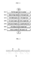
- FIG. 1 shows a flowchart of a method for manufacturing a flexible display device according to a first exemplary embodiment of the present invention.
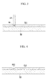
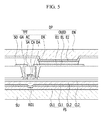
- FIG. 2 to FIG. 5 show a method for manufacturing a flexible display device according to a first exemplary embodiment of the present invention.
- a first organic layer OL1 may be formed, S110, on an auxiliary substrate SU .
- the first organic layer OL1 may be formed by coating an organic material on the auxiliary substrate (SU) made of glass, metal, or ceramic according to a coating process such as spin coating, slit coating, or inkjet coating.
- the first organic layer OL1 may be made of polymers, and it can be a single layer or multilayers including at least one of polyethylene terephthalate, polyimide, polycarbonate, epoxy, polyethylene, and polyacrylate which are organic materials.
- foreign particles PA such as undesired particles can be provided on a surface of the first organic layer OL1 or inside the same.
- a recessed first kind of repair groove RG1 may be formed on the first organic layer OL1 by removing foreign particles PA from the first organic layer OL1 (S120).
- the first organic layer OL1 may be tested by using a foreign particle testing device including a CCD whether there are foreign particles PA on the first organic layer OL1, and when the foreign particles PA are found on the first organic layer OL1, laser beams LA are irradiated on a part of the first organic layer OL1 where the foreign particles PA are provided to thus remove the foreign particles PA from the first organic layer OL1. Therefore, the recessed first kind of repair groove RG1 is formed on the part of the first organic layer OL1 on which the foreign particles PA were provided.
- a first inorganic layer CL1 may be formed on the first organic layer OL1 (S130).
- an inorganic material may be deposited as a layer on the first organic layer OL1 in which the first kind of repair groove RG1 may be formed by using a deposition process such as a sputtering method or a chemical vapor deposition method to thus form the first inorganic layer CL1.
- the first inorganic layer CL1 may be a single layer or multilayers including a metal oxide or metal nitride.
- the first inorganic layer CL1 includes at least one of SiNx, Al 2 O 3 , SiO 2 , and TiO 2 .
- the first inorganic layer CL1 is thinner than the first organic layer OL1 so a part of the first inorganic layer CL1 corresponding to the first kind of repair groove RG1 has a recessed shape corresponding to the first kind of repair groove RG1.
- a second organic layer OL2 may be formed on the first inorganic layer CL1 (S140).
- an organic material may be coated as a layer on the first inorganic layer CL1 by using a coating process such as spin coating, slit coating, or inkjet coating to thus form the second organic layer OL2.
- the second organic layer OL2 may be made of polymers, and it can be a single layer or multilayers including at least one of polyethylene terephthalate, polyimide, polycarbonate, epoxy, polyethylene, and polyacrylate.
- the second organic layer OL2 may be thicker than the first inorganic layer CL1 so a part of the recessed first inorganic layer CL1 may be filled with the second organic layer OL2 corresponding to the first kind of repair groove RG1.
- a second inorganic layer CL2 may be formed on the second organic layer OL2 (S150).
- an inorganic material may be deposited as a layer on the second organic layer OL2 by using the deposition process such as the sputtering method or the chemical vapor deposition method to thus form the second inorganic layer CL2.
- the second inorganic layer CL2 may be a single layer or multilayers including a metal oxide or metal nitride.
- the second inorganic layer CL2 includes at least one of SiNx, Al 2 O 3 , SiO 2 , and TiO 2 .
- a part of the recessed first inorganic layer CL1 may be filled corresponding to the first kind of repair groove RG1 by the second organic layer OL2 so the second inorganic layer CL2 may be flat on the second organic layer OL2.
- a flexible substrate FS may be formed according to the above-noted method.
- a display DP may be formed on the second inorganic layer CL2 (S160).
- a process for forming a thin film transistor may be applied to the second inorganic layer CL2 of the flexible substrate FS to form an active layer AC including a source area SA, a channel area CA, and a drain area DA and a plurality of thin film transistors TFT including a gate electrode GA, a source electrode SO, and a drain electrode DR, an organic light emitting diode OLED including a first electrode E1, an organic emission layer EL, and a second electrode E2 connected to the thin film transistor TFT may be then formed, and a thin-film encapsulator EN for encapsulating the organic light emitting diode OLED may be formed so the display DP for displaying images is formed.
- the display DP may be configured with a plurality of thin film transistors TFT, the organic light emitting diode OLED, and the thin-film encapsulator EN in the first exemplary embodiment of the present invention, and the display can be configured in various manners by a skilled person in the art in another exemplary embodiment of the present invention.
- a plurality of the display DP can be formed on the auxiliary substrate SU.
- the plurality of the display DP can be divided into an individual display DP by a process for cutting the auxiliary substrate.
- a display panel can include the individual display DP disposed on the cut-substrate.
- the auxiliary substrate SU may be removed from the first organic layer OL1(S170).
- laser beams are irradiated between the first organic layer OL1 and the auxiliary substrate SU and the first organic layer OL1 may be separated from the substrate SU to remove the auxiliary substrate SU from the first organic layer OL1, or the substrate SU may be etched to remove the auxiliary substrate SU from the first organic layer OL1.
- a flexible display device according to a second exemplary embodiment of the present invention to be described is manufactured according to the above-described process.
- the method for manufacturing a flexible display device removes the foreign particles PA from the first organic layer OL1 by using the laser beams LA to prevent generation of bubbles on the first organic layer OL1 caused by the foreign particles PA or generation of defects on the flexible substrate FS caused by cracks on the first inorganic layer CL1.
- the generation of defects on the flexible substrate FS may be controlled to prevent permeation of external moisture into the organic light emitting diode OLED caused by the defects generated on the flexible substrate FS and improve the life-span of the flexible display device.
- the method for manufacturing a flexible display device with improved life-span according to the first exemplary embodiment of the present invention is provided.
- the flexible display device according to the second exemplary embodiment of the present invention can be manufactured by using the method for manufacturing a flexible display device according to the second exemplary embodiment of the present invention.
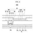
- FIG. 6 shows a flexible display device according to a second exemplary embodiment of the present invention.
- the flexible display device 1002 is flexible and includes a flexible substrate FS and a display DP.
- the flexible substrate FS includes a first organic layer OL1, a first inorganic layer CL1, a second organic layer OL2, and a second inorganic layer CL2.
- the first organic layer OL1 can be a single layer or multilayers including at least one of polyethylene terephthalate, polyimide, polycarbonate, epoxy, polyethylene, and polyacrylate, and it includes a recessed first kind of repair groove RG1.
- the first inorganic layer CL1 may be provided on the first organic layer OL1, and may be a single layer or multilayers including at least one of SiNx, Al 2 O 3 , SiO 2 , and TiO 2 which are inorganic materials.
- the first inorganic layer CL1 may be thinner than the first organic layer OL1, and a part of the first inorganic layer CL1 may be provided inside the first kind of repair groove RG1.
- the second organic layer OL2 may be provided on the first inorganic layer CL1, and it can be a single layer or multilayers including at least one of polyethylene terephthalate, polyimide, polycarbonate, epoxy, polyethylene, and polyacrylate.
- the second organic layer OL2 may be thicker than the first inorganic layer CL1, and a part of the second organic layer OL2 may be provided inside the first kind of repair groove RG1 together with a part of the first inorganic layer CL1.
- the second organic layer OL2 and the first inorganic layer CL1 are provided in the first kind of repair groove RG1 so the first kind of repair groove RG1 of the first organic layer OL1 is filled by the first inorganic layer CL1 and the second organic layer OL2.
- the second inorganic layer CL2 may be provided on the second organic layer OL2, and may be a single layer or multilayers including at least one of SiNx, Al 2 O 3 , SiO 2 , and TiO 2 which are inorganic materials.
- the second inorganic layer CL2 may be flat on the second organic layer OL2.
- the display DP may be provided on the flexible substrate FS and displays an image.
- the display DP includes an active layer AC having a source area SA, a channel area CA, and a drain area DA; a plurality of thin film transistors TFTs having a gate electrode G), a source electrode SO, and a drain electrode DR; an organic light emitting diode OLED having a first electrode E1, an organic emission layer EL, and a second electrode E2; and a thin-film encapsulator EN for sealing the organic light emitting diode OLED together with the flexible substrate FS.
- the display DP has various types known to a person skilled in the art.
- the flexible display device 1002 when forming the first organic layer OL1 included in the initial flexible substrate FS, removes the foreign particles PA from the first organic layer OL1 by using the laser beams LA when the foreign particles PA are included in the first organic layer OL1, and the first organic layer OL1 includes the first kind of repair groove RG1 thereby preventing generation of defects on the flexible substrate FS caused by generation of bubbles on the first organic layer OL1 by the foreign particles PA or generation of cracks on the first inorganic layer CL1.
- the generation of defects on the flexible substrate FS may be controlled to prevent permeation of external moisture into the organic light emitting diode OLED caused by the defects generated on the flexible substrate FS and improve the life-span of the flexible display device 1002.
- the flexible display device 1002 when the foreign particles PA are provided on the first organic layer OL1 of the initial flexible substrate FS, the flexible display device 1002 according to the second exemplary embodiment of the present invention from which the foreign particles PA are removed and of which the life-span is improved is provided.
- FIG. 7 shows a method for manufacturing a flexible display device according to a third exemplary embodiment of the present invention.
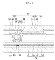
- FIG. 8 and FIG. 9 show a method for manufacturing a flexible display device according to a third exemplary embodiment of the present invention.
- the first organic layer OL1 may be formed on the auxiliary substrate SU (S310).
- a recessed first kind of repair groove RG1 may be formed in the first organic layer OL1 by removing the foreign particles PA provided on the first organic layer OL1(S320).
- a repair material RM may be filled in the first kind of repair groove RG1(S330).
- the repair material RM including a metal, an organic material, or an inorganic material may be filled in the recessed first kind of repair groove RG1 by using the coating process or the deposition process. Therefore, a first inorganic layer CL1, a second organic layer OL2, and a second inorganic layer CL2 formed on the repair material RM afterwards are formed to be flat.
- the first inorganic layer CL1 may be formed on the first organic layer OL1 (S340).
- the second organic layer OL2 may be formed on the first inorganic layer CL1 (S350).
- the second inorganic layer CL2 may be formed on the second organic layer OL2 (S360).
- the flexible substrate FS is formed according to the above-noted method.
- a display DP may be formed on the second inorganic layer CL2 (S370).
- a plurality of the display DP can be formed on the auxiliary substrate SU.
- the plurality of the display DP can be divided into an individual display DP by a process for cutting the substrate.
- a display panel can include the individual display DP disposed on the cut-substrate.
- the auxiliary substrate SU may be removed from the first organic layer OL1 (S380).
- a flexible display device according to a fourth exemplary embodiment of the present invention to be described is manufactured by the above-noted process.
- the method for manufacturing a flexible display device removes the foreign particles PA from the first organic layer OL1 by using the laser beams LA and fills the first kind of repair groove RG1 that may be formed in the removed part with the repair material RM, thereby preventing generation of defects on the flexible substrate FS caused by generation of bubbles on the first organic layer OL1 by the foreign particles PA or generation of cracks on the first inorganic layer CL1.
- the generation of defects on the flexible substrate FS may be controlled to prevent permeation of external moisture into the organic light emitting diode OLED caused by the defects generated on the flexible substrate FS and improve the life-span of the flexible display device.
- the method for manufacturing a flexible display device with improved life-span according to the third exemplary embodiment of the present invention is provided.
- the flexible display device according to the fourth exemplary embodiment of the present invention can be manufactured by using the method for manufacturing a flexible display device according to the third exemplary embodiment of the present invention.
- FIG. 10 shows a flexible display device according to a fourth exemplary embodiment of the present invention.
- the flexible display device 1004 is flexible and includes a flexible substrate FS and a display DP.
- the flexible substrate FS includes a first organic layer OL1, a first inorganic layer CL1, a second organic layer OL2, a second inorganic layer CL2, and a repair material RM.
- the repair material RM fills the first kind of repair groove RG1 formed in the first organic layer OL1, and it includes a metal, an organic material, or an inorganic material. Therefore, the first inorganic layer CL1, the second organic layer OL2, and the second inorganic layer CL2 provided on the repair material RM are flat.
- the flexible display device 1004 removes the foreign particles PA from the first organic layer OL1 by using the laser beams LA, the first organic layer OL1 includes the first kind of repair groove RG1, and the first kind of repair groove RG1 may be filled with the repair material RM thereby preventing generation of defects on the flexible substrate FS caused by generation of bubbles on the first organic layer OL1 by the foreign particles PA or generation of cracks on the first inorganic layer CL1.
- the generation of defects on the flexible substrate FS may be controlled to prevent permeation of external moisture into the organic light emitting diode OLED caused by the defects generated on the flexible substrate FS and improve the life-span of the flexible display device 1004.
- the flexible display device 1004 from which the foreign particles PA are removed and of which the life-span is improved when the foreign particles PA are provided on the first organic layer OL1 of the initial flexible substrate FS according to the fourth exemplary embodiment of the present invention is provided.
- FIG. 11 shows a flowchart of a method for manufacturing a flexible display device according to a fifth exemplary embodiment of the present invention.
- FIG. 12 to FIG. 15 show a method for manufacturing a flexible display device according to a fifth exemplary embodiment of the present invention.
- a first organic layer OL1 may be formed on an auxiliary substrate SU (S510).
- a first inorganic layer CL1 may be formed on the first organic layer OL1 (S520).
- the first inorganic layer CL1 may be formed on the first organic layer OL1 in which the first kind of repair groove RG1 may be formed by depositing an inorganic material as a layer by using the deposition process such as the sputtering method or chemical vapor deposition method.
- the first inorganic layer CL1 may be a single layer or multilayers including a metal oxide or metal nitride.
- the first inorganic layer CL1 includes at least one of SiNx, Al 2 O 3 , SiO 2 , and TiO 2 . In this instance, foreign particles PA such as undesired particles can be provided on the surface of the first inorganic layer CL1 or inside it.
- a recessed first kind of repair groove RG1 may be formed in the first organic layer OL1 and a first kind of repair hole RH1 for exposing the first kind of repair groove RG1 may be formed in the first inorganic layer CL1 by removing the foreign particles PA that are provided on the first inorganic layer CL1 (S530).
- the first kind of repair hole RH1 may be formed in a part of the first inorganic layer CL1 on which the foreign particles PA were provided, and the recessed first kind of repair groove RG1 may be formed in the first organic layer OL1 corresponding to the first kind of repair holeRH1.
- a second organic layer OL2 may be formed on the first inorganic layer CL1 (S540).
- an organic material may be coated as a layer on the first inorganic layer CL1 by using a coating process such as spin coating, slit coating, or inkjet coating to thus form the second organic layer OL2.
- the second organic layer OL2 may be made of polymers, and it can be a single layer or multilayers including at least one of polyethylene terephthalate, polyimide, polycarbonate, epoxy, polyethylene, and polyacrylate.
- the second organic layer OL2 may be thicker than the first inorganic layer CL1 so the first kind of repair hole RH1 of the first inorganic layer CL1 and the first kind of repair groove RG1 of the first organic layer OL1 are filled by the second organic layer OL2.
- a second inorganic layer CL2 may be formed on the second organic layer OL2 (S550).
- the second inorganic layer CL2 may be formed on the second organic layer OL2 by depositing an inorganic material as a layer by using the deposition process such as the sputtering method or the chemical vapor deposition method.
- the second inorganic layer CL2 may be a single layer or multilayers including a metal oxide or metal nitride.
- the second inorganic layer CL2 includes at least one of SiNx, Al 2 O 3 , SiO 2 , and TiO 2 .
- the first kind of repair groove RG1 and the first kind of repair hole RH1 are filled by the second organic layer OL2 so the second inorganic layer CL2 may be flat on the second organic layer OL2.
- the flexible substrate FS may be formed according to the above-noted method.
- a display DP may be formed on the second inorganic layer CL2 (S560).
- a plurality of the display DP can be formed on the auxiliary substrate SU.
- the plurality of the display DP can be divided into an individual display DP by a process for cutting the substrate.
- a display panel can include the individual display DP disposed on the cut-substrate.
- the auxiliary substrate SU may be removed from the first organic layer OL1 (S570).
- a flexible display device according to a sixth exemplary embodiment of the present invention to be described is manufactured.
- the method for manufacturing a flexible display device removes the foreign particles PA from the first inorganic layer CL1 by using the laser beams LA thereby preventing generation of defects on the flexible substrate FS caused by generation of bubbles on the first organic layer OL1 or the second organic layer OL2 by the foreign particles PA or generation of cracks on the first inorganic layer CL1.
- the generation of defects on the flexible substrate FS is controlled to prevent permeation of external moisture into the organic light emitting diode OLED caused by the defects generated on the flexible substrate FS and improve the life-span of the flexible display device.
- the flexible display device according to the sixth exemplary embodiment of the present invention can be manufactured by using the method for manufacturing a flexible display device according to the fifth exemplary embodiment of the present invention.
- FIG. 16 shows a flexible display device according to a sixth exemplary embodiment of the present invention.
- the flexible display device 1006 is flexible, and it includes a flexible substrate FS and a display DP.
- the flexible substrate FS includes a first organic layer OL1, a first inorganic layer CL1, a second organic layer OL2, and a second inorganic layer CL2.
- the first organic layer OL1 can be a single layer or multilayers including at least one of polyethylene terephthalate, polyimide, polycarbonate, epoxy, polyethylene, and polyacrylate, and it has a recessed first kind of repair groove RG1.
- the first inorganic layer CL1 is provided on the first organic layer OL1, and may be a single layer or multilayers including at least one of SiNx, Al 2 O 3 , SiO 2 , and TiO 2 which are inorganic materials.
- the first inorganic layer CL1 is thinner than the first organic layer OL1, and it includes a penetrated first kind of repair hole RH1 for exposing the first kind of repair groove RG1.
- the second organic layer OL2 may be provided on the first inorganic layer CL1, and it can be a single layer or multilayers including at least one of polyethylene terephthalate, polyimide, polycarbonate, epoxy, polyethylene, and polyacrylate.
- the second organic layer OL2 may be thicker than the first inorganic layer CL1, and a part of the second organic layer OL2 may be provided inside the first kind of repair groove RG1 through the first kind of repair hole RH1 to fill the first kind of repair hole RH1 and the first kind of repair groove RG1.
- the second inorganic layer CL2 may be provided on the second organic layer OL2, and may be a single layer or multilayers including at least one of SiNx, Al 2 O 3 , SiO 2 , and TiO 2 which are inorganic materials.
- the second inorganic layer CL2 may be flat on the second organic layer OL2.
- the flexible display device 1006 removes the foreign particles PA from the first inorganic layer CL1 by using the laser beams LA, and the first inorganic layer CL1 and the first organic layer OL1 include the first kind of repair hole RH1 and the first kind of repair groove RG1 thereby preventing generation of defects on the flexible substrate FS caused by generation of bubbles on the first organic layer OL1 or the second organic layer OL2 by the foreign particles PA or generation of cracks on the first inorganic layer CL1.
- the generation of defects on the flexible substrate FS may be controlled to prevent permeation of external moisture into the organic light emitting diode OLED caused by the defects generated on the flexible substrate FS and improve the life-span of the flexible display device 1006.
- the flexible display device 1006 from which the foreign particles PA are removed and of which the life-span is improved according to the sixth exemplary embodiment of the present invention is provided.
- FIG. 17 shows a flowchart of a method for manufacturing a flexible display device according to a seventh exemplary embodiment of the present invention.
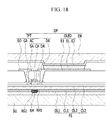
- FIG. 18 shows a method for manufacturing a flexible display device according to a seventh exemplary embodiment of the present invention.
- a first organic layer OL1 may be formed on an auxiliary substrate SU (S710).
- a first inorganic layer CL1 may be formed on the first organic layer OL1 (S720).
- the foreign particles PA provided on the first inorganic layer CL1 are removed to form a recessed first kind of repair groove RG1 in the first organic layer OL1 and a first kind of repair hole RH1 for exposing the first kind of repair groove RG1 in the first inorganic layer CL1 (S730).
- the first kind of repair groove RG1 and the first kind of repair hole RH1 are filled with a repair material RM (S740).
- the recessed first kind of repair groove RG1 may be filled with the repair material RM including a metal, an organic material, or an inorganic material through the opened first kind of repair hole RH1 by using the coating process or the deposition process. Therefore, the second organic layer OL2 and the second inorganic layer CL2 will be formed to be flat on the repair material RM afterwards.
- a second organic layer OL2 may be formed on the first inorganic layer CL1 (S750).
- a second inorganic layer CL2 may be formed on the second organic layer OL2 (S760).
- the flexible substrate FS may be formed according to the above-noted method.
- a display DP may be formed on the second inorganic layer CL2 (S770).
- a plurality of the display DP can be formed on the auxiliary substrate SU.
- the plurality of the display DP can be divided into an individual display DP by a process for cutting the substrate.
- a display panel can include the individual display DP disposed on the cut-substrate.
- the auxiliary substrate SU may be removed from the first organic layer OL1 (S780).
- a flexible display device according to an eighth exemplary embodiment of the present invention to be described is manufactured.
- the method for manufacturing a flexible display device removes the foreign particles PA from the first inorganic layer CL1 by using the laser beams LA and fills the repair material RM in the first kind of repair hole RH1 and the first kind of repair groove RG1 that are formed in the removed part, thereby preventing generation of defects on the flexible substrate FS caused by generation of bubbles on the first organic layer OL1 or the second organic layer OL2 by the foreign particles PA or generation of cracks on the first inorganic layer CL1.
- the generation of defects on the flexible substrate FS is controlled to prevent permeation of external moisture into the organic light emitting diode OLED caused by the defects generated on the flexible substrate FS and improve the life-span of the flexible display device.
- the method for manufacturing a flexible display device with improved life-span according to the seventh exemplary embodiment of the present invention is provided.
- the flexible display device according to the eighth exemplary embodiment of the present invention can be manufactured by using the method for manufacturing a flexible display device according to the seventh exemplary embodiment of the present invention.
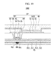
- FIG. 19 shows a flexible display device according to an eighth exemplary embodiment of the present invention.
- the flexible display device 1008 is flexible and it includes a flexible substrate FS and a display DP.
- the flexible substrate FS includes a first organic layer OL1, a first inorganic layer CL1, a second organic layer OL2, a second inorganic layer CL2, and a repair material RM.
- the repair material RM fills the first kind of repair groove RG1 formed in the first organic layer OL1 and the first kind of repair hole RH1 formed in the first inorganic layer CL1, and it includes a metal, an organic material, or an inorganic material. Therefore, the second organic layer OL2 and the second inorganic layer CL2 provided on the repair material RM are flat.
- the flexible display device 1008 removes the foreign particles PA from the first inorganic layer CL1 by using the laser beams LA, the first inorganic layer CL1 and the first organic layer OL1 includes the first kind of repair hole RH1 and the first kind of repair groove RG1, and the first kind of repair hole RH1 and the first kind of repair hole RH1 are filled with the repair material RM, thereby preventing generation of defects on the flexible substrate FS caused by generation of bubbles on the first organic layer OL1 or the second organic layer OL2 by the foreign particles PA or generation of cracks on the first inorganic layer CL1.
- the generation of defects on the flexible substrate FS is controlled to prevent permeation of external moisture into the organic light emitting diode OLED caused by the defects generated on the flexible substrate FS and improve the life-span of the flexible display device 1008.
- the flexible display device 1008 from which the foreign particles PA are removed and of which the life-span is improved according to the eighth exemplary embodiment of the present invention is provided.
- FIG. 20 shows a flowchart of a method for manufacturing a flexible display device according to a ninth exemplary embodiment of the present invention.
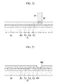
- FIG. 21 to FIG. 24 show a method for manufacturing a flexible display device according to a ninth exemplary embodiment of the present invention.
- a first organic layer OL1 may be formed on an auxiliary substrate SU (S910).
- a first inorganic layer CL1 may be formed on the first organic layer OL1 (S920).
- a second organic layer OL2 may be formed on the first inorganic layer CL1 (S930).
- a second inorganic layer CL2 may be formed on the second organic layer OL2 (S940).
- bubbles BU may be generated on the second organic layer OL2 and the second inorganic layer CL2 by the heat generated during the deposition process for forming the second inorganic layer CL2 or the hardening process for hardening the second organic layer OL2.
- the bubbles BU formed on the second inorganic layer CL2 are removed to form a recessed second kind of repair groove RG2 in the second organic layer OL2 and a second kind of repair hole RH2 for exposing the second kind of repair groove RG2 on the second inorganic layer CL2 (S950).
- a bubble testing device including a CCD it is tested whether bubbles B) are formed on the second inorganic layer CL2 by using a bubble testing device including a CCD, and when the undesired bubbles BU are formed on the second inorganic layer CL2, laser beams LA are irradiated to a part of the second inorganic layer CL2 on which the bubbles BU are provided to thereby remove the bubbles BU from the second inorganic layer CL2. Therefore, a second kind of repair hole RH2 may be formed in the part of the second inorganic layer CL2, and a recessed second kind of repair groove RG2 may be formed in the second organic layer OL2 corresponding to the second kind of repair hole RH2.
- the flexible substrate FS may be formed according to the above-noted method.
- a display DP may be formed on the second inorganic layer CL2 (S960).
- a part that is provided corresponding to the second kind of repair hole RH2 and the second kind of repair groove RG2 in the display DP may be provided inside the second kind of repair groove RG2 or not.
- the active layer AC may be provided inside the second kind of repair groove RG2, and when the second kind of repair hole RH2 and the second kind of repair groove RG2 are provided corresponding to the first electrode E1, the active layer AC is not provided inside the second kind of repair groove RG2.
- An auxiliary substrate SU may be removed from the first organic layer OL1 (S970).
- a flexible display device according to a tenth exemplary embodiment of the present invention to be described is manufactured according to the above-noted process.
- the method for manufacturing a flexible display device removes the bubbles BU from the second inorganic layer CL2 by using the laser beams LA when the bubbles BU are formed on the initial flexible substrate FS because of foreign particles, thereby preventing generation of defects on the flexible substrate FS.
- the generation of defects on the flexible substrate FS is controlled to prevent permeation of external moisture into the organic light emitting diode OLED caused by the defects generated on the flexible substrate FS and improve the life-span of the flexible display device.
- the method for manufacturing a flexible display device with improved life-span according to the ninth exemplary embodiment of the present invention is provided.
- the flexible display device according to the tenth exemplary embodiment of the present invention can be manufactured by using the method for manufacturing a flexible display device according to the ninth exemplary embodiment of the present invention.
- FIG. 25 shows a flexible display device according to a tenth exemplary embodiment of the present invention.
- the flexible display device 1010 is flexible, and it includes a flexible substrate FS and a display DP.
- the flexible substrate FS includes a first organic layer OL1, a first inorganic layer CL1, a second organic layer OL2, and a second inorganic layer CL2.
- the second organic layer OL2 and the second inorganic layer CL2 include a second kind of repair groove RG2 and a second kind of repair hole RH2, respectively.
- the flexible display device 1010 when the bubbles BU are formed on the flexible substrate FS because of foreign particles, the flexible display device 1010 according to the tenth exemplary embodiment of the present invention removes the bubbles BU from the second inorganic layer CL2 by using the laser beams LA so that the second organic layer OL2 and the second inorganic layer CL2 include the second kind of repair groove RG2 and the second kind of repair hole RH2, respectively, thereby preventing generation of cracks on the second inorganic layer CL2 by the bubbles BU and subsequent generation of defects on the flexible substrate FS.
- the generation of defects on the flexible substrate FS is controlled to prevent permeation of external moisture into the organic light emitting diode OLED caused by the defects generated on the flexible substrate FS and improve the life-span of the flexible display device 1010.
- the flexible display device 1010 from which the bubbles BU are removed and of which the life-span is improved when the bubbles BU are formed on the second inorganic layer CL2 of the flexible substrate FS according to the tenth exemplary embodiment of the present invention is provided.
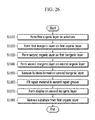
- FIG. 26 shows a flowchart of a method for manufacturing a flexible display device according to an eleventh exemplary embodiment of the present invention.
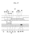
- FIG. 27 shows a method for manufacturing a flexible display device according to an eleventh exemplary embodiment of the present invention.
- a first organic layer OL1 may be formed on an auxiliary substrate SU (S1110).
- a first inorganic layer CL1 may be formed on the first organic layer OL1 (S1120).
- a second organic layer OL2 may be formed on the first inorganic layer CL1 (S1130).
- a second inorganic layer CL2 may be formed on the second organic layer OL2 (S 1140).
- bubbles BU are generated on the second organic layer OL2 and the second inorganic layer CL2 by the heat generated by the deposition process for forming the second inorganic layer CL2 or the hardening process for hardening the second organic layer OL2.
- the bubbles BU formed on the second inorganic layer CL2 are removed to form a recessed second kind of repair groove RG2 in the second organic layer OL2 and a second kind of repair hole RH2 for exposing the second kind of repair groove RG2 on the second inorganic layer CL2 (S1150).
- a bubble testing device including a CCD it is tested whether bubbles BU are formed on the second inorganic layer CL2 by using a bubble testing device including a CCD, and when the undesired bubbles BU are formed on the second inorganic layer CL2, laser beams LA are irradiated to a part of the second inorganic layer CL2 on which the bubbles BU are provided to thereby remove the bubbles BU from the second inorganic layer CL2. Therefore, a second kind of repair hole RH2 may be formed in the part of the second inorganic layer CL2, and a recessed second kind of repair groove RG2 may be formed in the second organic layer OL2 corresponding to the second kind of repair hole RH2.
- a repair material RM may be filled in the second kind of repair groove RG2 (S1160).
- the repair material RM including a metal, an organic material, or an inorganic material may be filled in the recessed second kind of repair groove RG2 by using the coating process or the deposition process. Therefore, the display DP formed on the repair material RM may be formed to be flat.
- the flexible substrate FS is formed according to the above-noted method.
- a display DP may be formed on the second inorganic layer CL2 (S1170).
- a plurality of the display DP can be formed on the auxiliary substrateSU.
- the plurality of the display DP can be divided into an individual display DP by a process for cutting the auxiliary substrate.
- a display panel can include the individual display DP disposed on the cut-substrate.
- the auxiliary substrate SU may be removed from the first organic layer OL1 (S1180).
- a flexible display device according to a twelfth exemplary embodiment of the present invention to be described is manufactured according to the above-noted process.
- the method for manufacturing a flexible display device removes the bubbles BU from the second inorganic layer CL2 by using laser beams LA, and fills the removed part with the repair material RM, thereby preventing generation of defects on the flexible substrate FS.
- the generation of defects on the flexible substrate FS is controlled to prevent permeation of external moisture into the organic light emitting diode OLED caused by the defects generated on the flexible substrate FS and improve the life-span of the flexible display device.
- the flexible display device according to the twelfth exemplary embodiment of the present invention can be manufactured by using the method for manufacturing a flexible display device according to the eleventh exemplary embodiment of the present invention.
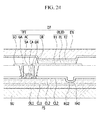
- FIG. 28 shows a flexible display device according to a twelfth exemplary embodiment of the present invention.
- the flexible display device 1012 is flexible, and it includes a flexible substrate FS and a display DP.
- the flexible substrate FS includes a first organic layer OL1, a first inorganic layer CL1, a second organic layer OL2, a second inorganic layer CL2, and a repair material RM.
- the second organic layer(OL2 and the second inorganic layer CL2 respectively include a second kind of repair groove RG2 and a second kind of repair hole RH2.
- a repair material RM fills the second kind of repair groove RG2 through the second kind of repair hole RH2.
- the display DP is provided in the second kind of repair groove RG2 and may be formed to be flat.
- the flexible display device 1012 when bubbles BU are formed on the flexible substrate FS by the foreign particles, the flexible display device 1012 according to the twelfth exemplary embodiment of the present invention removes the bubbles BU from the second inorganic layer CL2 by using laser beams LA so the second organic layer OL2 and the second inorganic layer CL2 respectively include a second kind of repair groove RG2 and a second kind of repair hole RH2, and the second kind of repair groove RG2 may be filled with the repair material RM thereby preventing generation of cracks on the second inorganic layer CL2 by the bubbles BU and generation of defects on the flexible substrate FS.
- the generation of defects on the flexible substrate FS is controlled to prevent permeation of external moisture into the organic light emitting diode OLED caused by the defects generated on the flexible substrate FS and improve the life-span of the flexible display device 1012.
- the flexible display device 1012 from which the bubbles BU are removed and of which the life-span is improved according to the twelfth exemplary embodiment of the present invention is provided.
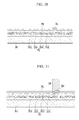
- FIG. 29 shows a flowchart of a method for manufacturing a flexible display device according to a thirteenth exemplary embodiment of the present invention.
- FIG. 30 to FIG. 33 show a method for manufacturing a flexible display device according to a thirteenth exemplary embodiment of the present invention.
- a first organic layer OL1 may be formed on an auxiliary substrate SU (S 1310).
- a first inorganic layer CL1 may be formed on the first organic layer OL1 (S1320).
- a second organic layer OL2 may be formed on the first inorganic layer CL1 (S1330).
- a second inorganic layer CL2 may be formed on the second organic layer OL2 (S1340).
- the flexible substrate FS may be formed according to the above-noted method.
- a polysilicon layer PS may be formed on the second inorganic layer CL2 (S1350).
- an amorphous silicon layer may be formed on the second inorganic layer CL2, and the amorphous silicon layer may be crystallized by using heat or laser beams to form a polysilicon layer P) from the amorphous silicon layer.
- bubbles BU are generated on the second organic layer OL2, the second inorganic layer CL2 and the polysilicon layer PS by the heat generated during the deposition process for forming the second inorganic layer CL2, the hardening process for hardening the second organic layer OL2, or the crystallization process for crystallizing the amorphous silicon layer.
- the bubbles BU formed on the polysilicon layer PS are removed to form a recessed second kind of repair groove RG2 in the second organic layer OL2, a second kind of repair hole RH2 for exposing the second kind of repair groove RG2 in the second inorganic layer CL2, and a further repair hole RH3 for exposing the second kind of repair groove RG2 in the polysilicon layer PS (S1360).
- a bubble testing device including a CCD whether bubbles BU are formed on the polysilicon layer PS, and when the bubbles BU are found, laser beams LA are irradiated to a part of the polysilicon layer PS on which the bubbles BU are provided to remove the bubbles BU from the polysilicon layer PS.
- a further repair hole RH3 may be formed in a part of the polysilicon layer PS on which the bubbles BU were provided, a second kind of repair hole RH2 may be formed in a part of the second inorganic layer CL2 corresponding to the further repair hole RH3, and a recessed second kind of repair groove RG2 may be formed in the second organic layer OL2 corresponding to the second kind of repair hole RH2.
- an active layer AC may be formed by patterning the polysilicon layer PS (S1370).
- a photolithography process may be used to pattern the polysilicon layer PS and form the active layer AC, and a source electrode SO, a drain electrode DR, and a gate electrode GA are formed. In this instance, a part of the polysilicon layer PS in which the further repair hole RH3 may be formed is removed.
- the active layer AC may include a further repair hole RH3.
- An organic light emitting diode OLED connected to the active layer AC may be formed (S1380).
- the organic light emitting diode OLED may be formed by forming the first electrode E1, the organic emission layer EL, and the second electrode E2, and a display DP may be formed by forming a thin-film encapsulator EN.
- the auxiliary substrate SU may be removed from the first organic layer OL1 (S1390).
- a flexible display device according to a fourteenth exemplary embodiment of the present invention to be described is manufactured.
- the method for manufacturing a flexible display device removes the bubbles BU from the polysilicon layer PS by using the laser beams LA, thereby preventing generation of undesired defects on the flexible display device. Therefore, permeation of external moisture into the organic light emitting diode OLED caused by the undesired defects that are generated in the flexible display device is prevented so the life-span of the flexible display device is improved.
- the method for manufacturing a flexible display device with improved life-span according to the thirteenth exemplary embodiment of the present invention is provided.
- the flexible display device according to the fourteenth exemplary embodiment of the present invention can be manufactured by using the method for manufacturing a flexible display device according to the thirteenth exemplary embodiment of the present invention.
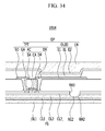
- FIG. 34 shows a flexible display device according to a fourteenth exemplary embodiment of the present invention.
- the flexible display device 1014 is flexible, and it includes a flexible substrate FS and a display DP.
- the flexible substrate FS includes a first organic layer OL1, a first inorganic layer CL1, a second organic layer OL2, and a second inorganic layer CL2.
- the second organic layer OL2 and the second inorganic layer CL2 respectively include a second kind of repair groove RG2 and a second kind of repair hole RH2.
- the flexible display device 1014 when bubbles BU are formed on the polysilicon layer formed to be an active layer AC, the flexible display device 1014 according to the fourteenth exemplary embodiment of the present invention removes the bubbles BU from the polysilicon layer by using the laser beams LA, and the second organic layer OL2 and the second inorganic layer CL2 respectively include a second kind of repair groove RG2 and a second kind of repair hole RH2 thereby preventing generation of undesired defects on the flexible display device 1014 by the bubbles BU. Therefore, permeation of external moisture into the organic light emitting diode OLED caused by the undesired defects that are generated in the flexible display device 1014 is prevented so the life-span of the flexible display device 1014 is improved.
- the bubbles BU on the polysilicon layer are removed, so that the life-span of the flexible display device 1014 can be improved.
- FIG. 35 shows a flowchart of a method for manufacturing a flexible display device according to a fifteenth exemplary embodiment of the present invention.
- FIG. 36 shows a method for manufacturing a flexible display device according to a fifteenth exemplary embodiment of the present invention.
- a first organic layer OL1 may be formed on the auxiliary substrate SU(S1510).
- a first inorganic layer CL1 may be formed on the first organic layer OL1 (S1520).
- a second organic layer OL2 may be formed on the first inorganic layer CL1 (S1530).
- a second inorganic layer CL2 may be formed on the second organic layer OL2 (S1540).
- the flexible substrate FS may be formed according to the above-noted method.
- a polysilicon layer PS may be formed on the second inorganic layer CL2 (S1550).
- the bubbles BU formed on the polysilicon layer PS are removed to form a recessed second kind of repair groove RG2 on the second organic layer OL2, a second kind of repair hole RH2 for exposing the second kind of repair groove RG2 in the second inorganic layer CL2, and a further repair hole for exposing the second kind of repair groove RG2 in the polysilicon layer PS (S1560).
- the second kind of repair groove RG2 may be filled with a repair material RM (S 1570).
- the recessed second kind of repair groove RG2 may be filled with the repair material RM including a metal, an organic material, or an inorganic material by using the coating process or the deposition process.
- the second kind of repair hole RH2 and the further repair hole are filled with the repair material RM. Therefore, the display DP formed on the repair material RM will be formed to be flat.
- a polysilicon layer PS may be patterned to form an active layer AC (S1580).
- a part of the polysilicon layer PS in which the further repair hole may be formed is removed.
- the active layer AC includes the further repair hole.
- An organic light emitting diode OLED connected to the active layer AC may be formed (S1590).
- the auxiliary substrate SU may be removed from the first organic layer OL1 (S1595).
- a flexible display device according to a sixteenth exemplary embodiment of the present invention to be described is manufactured according to the above-noted process.
- the method for manufacturing a flexible display device removes the bubbles BU from the polysilicon layer PS by using the laser beams LA and fills the removed part with the repair material RM thereby preventing generation of undesired defects on the flexible display device. Therefore, permeation of external moisture into the organic light emitting diode OLED caused by the undesired defects that are generated in the flexible display device is prevented so the life-span of the flexible display device is improved.
- the flexible display device according to the sixteenth exemplary embodiment of the present invention is manufactured by using the method for manufacturing a flexible display device according to the fifteenth exemplary embodiment of the present invention.
- FIG. 37 shows a flexible display device according to a sixteenth exemplary embodiment of the present invention.
- the flexible display device 1016 is flexible, and it includes a flexible substrate FS, a display DP, and a repair material RM.
- the repair material RM fills the second kind of repair groove RG2 through the second kind of repair hole RH2. That is, the repair material RM fills the second kind of repair hole RH2 and the second kind of repair groove RG2.
- the flexible display device 1016 when the bubbles BU are formed on the polysilicon layer formed as an active layer AC, the flexible display device 1016 according to the sixteenth exemplary embodiment of the present invention removes the bubbles BU from the polysilicon layer by using the laser beams LA, the second organic layer OL2, the second inorganic layer CL2, and active layer AC respectively include the second kind of repair groove RG2, the second kind of repair hole RH2, and the further repair hole RH3, and the second kind of repair groove RG2 is filled with the repair material RM thereby preventing generation of undesired defects on the flexible display device 1016 by the bubbles BU. Therefore, permeation of external moisture into the organic light emitting diode OLED caused by the undesired defects that are generated in the flexible display device 1016 is prevented so the
- the flexible display device 1016 from which the bubbles BU are removed and of which the life-span is improved when the bubbles BU are formed on the polysilicon layer of the flexible display device 1016 according to the sixteenth exemplary embodiment of the present invention is provided.
Landscapes
- Engineering & Computer Science (AREA)
- Chemical & Material Sciences (AREA)
- Inorganic Chemistry (AREA)
- Manufacturing & Machinery (AREA)
- Physics & Mathematics (AREA)
- Microelectronics & Electronic Packaging (AREA)
- Optics & Photonics (AREA)
- General Physics & Mathematics (AREA)
- Theoretical Computer Science (AREA)
- Electroluminescent Light Sources (AREA)
- Devices For Indicating Variable Information By Combining Individual Elements (AREA)
Abstract
Description
- The present invention generally relates to a flexible display device, and a method for manufacturing a flexible display device.
- A display device is a device displaying images, and recently, a display device including an organic light emitting diode has received attention.
- Since the organic light emitting diode has a self-emission characteristic and does not require a separate light source, unlike a liquid crystal display device, a thickness and a weight of the entire display device may be reduced. Further, the organic light emitting diode has high-quality characteristics such as low power consumption, high luminance, and a high response speed.
- The above information disclosed in this Related Art section is only for enhancement of understanding of the background of the invention and therefore it may contain information that does not form the prior art that is already known in this country to a person of ordinary skill in the art.
- The present invention has been made in an effort to provide a flexible display device, and a method for manufacturing a flexible display device.
- The present invention provides a method according to claim 1 for manufacturing a flexible display device. Said method includes forming, on an auxiliary substrate a flexible substrate by: forming a first organic layer on the auxiliary substrate; forming a first inorganic layer on the first organic layer; forming a second organic layer on the first inorganic layer; and forming a second inorganic layer on the second organic layer, removing impurities and forming a recessed repair groove. Either, the impurities are particles or the impurities are bubbles removed from the second organic layer, and then the method further comprises forming a display for displaying an image on the flexible substrate. Or, the impurities are bubbles removed from a polysilicon layer, then the method further comprises forming the polysilicon layer on the second inorganic layer ; forming an active layer by patterning the polysilicon layer and forming an organic light emitting diode connected to the active layer. The method yet further comprises removing the auxiliary substrate from the first organic layer. Either, the impurities are particles and the recessed repair groove is formed in the first organic layer. Then, if the particles are removed from the first inorganic layer, the method even yet further comprises forming a repair hole in the first inorganic layer for exposing the repair groove. Or the impurities are bubbles and the recessed repair groove is formed in the second organic layer. Then the method even yet further comprises forming, in the second inorganic layer, a repair hole exposing the repair groove, and, if the bubbles are removed from the polysilicon layer, forming a further repair hole in the polysilicon layer for exposing the repair hole.
- In an embodiment of the method, the removing of the bubbles or of the foreign particles may be performed by irradiating laser beams on the respective layer, i.e., for removing particles, on the first organic layer or the first inorganic layer and, for removing bubbles, on the second organic layer or on the polysilicon layer.
- In a second embodiment of the method" the forming of the first organic layer on the auxiliary substrate may be performed by coating an organic material on the substrate.
- The forming of the first inorganic layer on the first organic layer may be performed by depositing an inorganic material on the first organic layer.
- The method may further include filling the repair groove with a repair material.
- The forming of a display may be performed by forming an organic light emitting diode on the flexible substrate.
- The present invention further provides a flexible display device according to claim 6, the flexible display device including a flexible substrate comprising a first organic layer; a first inorganic layer provided on the first organic layer; a second organic layer provided on the first inorganic layer; and a second inorganic layer provided on the second organic layer. The flexible display device further comprises, either, a recessed repair groove included in one of the first and the second organic layer and a display provided on the flexible substrate for displaying an image, or, a recessed repair groove included in the second organic layer and an active layer provided on the flexible substrate and including a polysilicon layer; and an organic light emitting diode connected to the active layer.
- In an embodiment of the flexible display device, the display includes an organic light emitting diode.
- The recessed repair groove may be included in the first organic layer.
- A repair hole may be included in the first inorganic layer, the repair hole exposing the repair groove.
- The recessed repair groove may be included in the second organic layer and the flexible display device may further comprise a repair hole included in the second inorganic layer, the repair hole exposing the repair groove.
- A further repair hole may be included in the polysilicon layer, the further repair hole exposing the repair hole.
- A part of each of the first inorganic layer and the second organic layer may be provided inside the repair groove.
- The first organic layer and the second organic layer respectively include an organic material.
- The first inorganic layer and the second inorganic layer respectively include an inorganic material.
- The flexible substrate may further include a repair material for filling the repair groove.
- Another embodiment of the present invention provides a flexible display device including: the flexible substrate; and a display provided on the flexible substrate and displaying an image.
- The display includes an organic light emitting diode.
- Another embodiment of the present invention provides a further method for manufacturing a flexible display device, the method including: forming a first organic layer on an auxiliary substrate; forming a first inorganic layer on the first organic layer; forming a recessed repair groove in the first organic layer and a repair hole for exposing the repair groove in the first inorganic layer by removing foreign particles provided on the first inorganic layer; forming a second organic layer on the first inorganic layer; and forming a second inorganic layer on the second organic layer.
- In an embodiment of the further method, the removing of foreign particles may be performed by irradiating laser beams on the first inorganic layer.
- The further method may further include filling the repair groove with a repair material.
- The further method for manufacturing a flexible display device may further include: forming a display for displaying an image on the flexible substrate; and removing the auxiliary substrate from the first organic layer.
- Another embodiment of the present invention provides a further flexible display device including: a first organic layer including a recessed repair groove; a first inorganic layer provided on the first organic layer and including a repair hole for exposing the repair groove; a second organic layer provided on the first inorganic layer; and a second inorganic layer provided on the second organic layer.
- In an embodiment of the further device, a part of the second organic layer may be provided inside the repair groove through the repair hole.
- The flexible display device may further include a repair material for filling the repair groove.
- The flexible display device may further include a display provided on the flexible substrate and displaying an image.
- Another embodiment of the present invention provides a method for manufacturing a flexible display device including: forming a first organic layer on an auxiliary substrate; forming a first inorganic layer on the first organic layer; forming a second organic layer on the first inorganic layer; forming a second inorganic layer on the second organic layer; and forming a recessed repair groove in the second organic layer and a repair hole for exposing the repair groove in the second inorganic layer by removing the bubbles formed on the second inorganic layer.
- In an embodiment, the removing of bubbles may be performed by irradiating laser beams on the second inorganic layer.
- The method may further include filling the repair groove with a repair material.
- The method for manufacturing a flexible display device may include: forming a display for displaying an image on the flexible substrate; and removing the auxiliary substrate from the first organic layer.
- Another embodiment of the present invention provides a flexible display device including: a first organic layer; a first inorganic layer provided on the first organic layer; a second organic layer provided on the first inorganic layer and including a repair groove; and a second inorganic layer provided on the second organic layer and including a repair hole for exposing the repair groove.
- In an embodiment, flexible display device further includes a repair material for filling the repair groove.
- The flexible display device may include a display provided on the flexible substrate for displaying an image.
- Another embodiment of the present invention provides a method for manufacturing a flexible display device including: forming a first organic layer on an auxiliary substrate; forming a first inorganic layer on the first organic layer; forming a second organic layer on the first inorganic layer; forming a second inorganic layer on the second organic layer; forming a polysilicon layer on the second inorganic layer; removing bubbles formed on the polysilicon layer and forming a recessed repair groove in the second organic layer, a repair hole for exposing the repair groove in the second inorganic layer, and a further repair hole for exposing the repair hole in the polysilicon layer; forming an active layer by patterning the polysilicon layer; forming an organic light emitting diode connected to the active layer; and removing the auxiliary substrate from the first organic layer.
- In an embodiment, the removing of bubbles may be performed by irradiating laser beams on the polysilicon layer.
- The method may further include filling the repair groove with a repair material.
- Another embodiment of the present invention provides a flexible display device including: a flexible substrate including a first organic layer, a first inorganic layer provided on the first organic layer, a second organic layer provided on the first inorganic layer and including a recessed repair groove, and a second inorganic layer provided on the second organic layer and including a repair hole for exposing the repair groove; an active layer provided on the flexible substrate and including a polysilicon layer; and an organic light emitting diode connected to the active layer.
- In an embodiment, the flexible display device may further include a repair material for filling the repair groove.
- According to the embodiments of the present invention, the flexible display device, and the method for manufacturing a flexible display device are provided.
- A more complete appreciation of the invention, and many of the attendant advantages thereof, will be readily apparent as the same becomes better understood by reference to the following detailed description when considered in conjunction with the accompanying drawings, in which like reference symbols indicate the same or similar components, wherein:
-
FIG. 1 shows a flowchart of a method for manufacturing a flexible display device according to a first exemplary embodiment of the present invention. -
FIG. 2 to FIG. 5 show a method for manufacturing a flexible display device according to a first exemplary embodiment of the present invention. -
FIG. 6 shows a flexible display device according to a second exemplary embodiment of the present invention. -
FIG. 7 shows a method for manufacturing a flexible display device according to a third exemplary embodiment of the present invention. -
FIG. 8 andFIG. 9 show a method for manufacturing a flexible display device according to a third exemplary embodiment of the present invention. -
FIG. 10 shows a flexible display device according to a fourth exemplary embodiment of the present invention. -
FIG. 11 shows a flowchart of a method for manufacturing a flexible display device according to a fifth exemplary embodiment of the present invention. -
FIG. 12 to FIG. 15 show a method for manufacturing a flexible display device according to a fifth exemplary embodiment of the present invention. -
FIG. 16 shows a flexible display device according to a sixth exemplary embodiment of the present invention. -
FIG. 17 shows a flowchart of a method for manufacturing a flexible display device according to a seventh exemplary embodiment of the present invention. -
FIG. 18 shows a method for manufacturing a flexible display device according to a seventh exemplary embodiment of the present invention. -
FIG. 19 shows a flexible display device according to an eighth exemplary embodiment of the present invention. -
FIG. 20 shows a flowchart of a method for manufacturing a flexible display device according to a ninth exemplary embodiment of the present invention. -
FIG. 21 to FIG. 24 show a method for manufacturing a flexible display device according to a ninth exemplary embodiment of the present invention. -
FIG. 25 shows a flexible display device according to a tenth exemplary embodiment of the present invention. -
FIG. 26 shows a flowchart of a method for manufacturing a flexible display device according to an eleventh exemplary embodiment of the present invention. -
FIG. 27 shows a method for manufacturing a flexible display device according to an eleventh exemplary embodiment of the present invention. -
FIG. 28 shows a flexible display device according to a twelfth exemplary embodiment of the present invention. -
FIG. 29 shows a flowchart of a method for manufacturing a flexible display device according to a thirteenth exemplary embodiment of the present invention. -
FIG. 30 to FIG. 33 show a method for manufacturing a flexible display device according to a thirteenth exemplary embodiment of the present invention. -
FIG. 34 shows a flexible display device according to a fourteenth exemplary embodiment of the present invention. -
FIG. 35 shows a flowchart of a method for manufacturing a flexible display device according to a fifteenth exemplary embodiment of the present invention. -
FIG. 36 shows a method for manufacturing a flexible display device according to a fifteenth exemplary embodiment of the present invention. -
FIG. 37 shows a flexible display device according to a sixteenth exemplary embodiment of the present invention. - The present invention will be described more fully hereinafter with reference to the accompanying drawings, in which exemplary embodiments of the invention are shown. As those skilled in the art would realize, the described embodiments may be modified in various different ways, all without departing from the scope of the present invention as defined in the claims.
- The drawings and description are to be regarded as illustrative in nature and not restrictive and like reference numerals designate like elements throughout the specification.
- Elements will be representatively explained in the first exemplary embodiment using reference numerals, and in the remaining embodiments, elements different from the first exemplary embodiment will be explained.
- The size and the thickness of each element in the drawing are random samples for better understanding and ease of description, and the present invention is not limited thereto.
- In the drawings, the thickness of layers, films, panels, regions, etc., are exaggerated for clarity. The thickness of the layers, films, panels, regions, etc., is enlarged in the drawings for better understanding and ease of description. It will be understood that when an element such as a layer, film, region, or substrate is referred to as being "on" another element, it can be directly on the other element or intervening elements may also be present.
- In addition, unless explicitly described to the contrary, the word "comprise" and variations such as "comprises" or "comprising" will be understood to imply the inclusion of stated elements but not the exclusion of any other elements. Throughout this specification, it is understood that the term "on" and similar terms are used generally and are not necessarily related to a gravitational reference.
- In general, an organic light emitting diode (OLED) display includes a substrate, an organic light emitting diode provided on the substrate, and an encapsulator for encapsulating the organic light emitting diode with the substrate having the organic light emitting diode therebetween.
- The substrate employed in an OLED may be a flexible substrate that makes the display bendable. However, when a defect occurs on the flexible substrate, moisture may permeate into the organic light emitting diode through a defect-generated part to reduce the life-span of the organic light emitting diode (OLED) display.
- Referring to
FIG. 1 to FIG. 5 , a method for manufacturing a flexible display device according to a first exemplary embodiment of the present invention will now be described. -
FIG. 1 shows a flowchart of a method for manufacturing a flexible display device according to a first exemplary embodiment of the present invention.FIG. 2 to FIG. 5 show a method for manufacturing a flexible display device according to a first exemplary embodiment of the present invention. - As shown in
FIG. 1 and FIG. 2 , a first organic layer OL1 may be formed, S110, on an auxiliary substrate SU . - In detail, the first organic layer OL1 may be formed by coating an organic material on the auxiliary substrate (SU) made of glass, metal, or ceramic according to a coating process such as spin coating, slit coating, or inkjet coating. The first organic layer OL1 may be made of polymers, and it can be a single layer or multilayers including at least one of polyethylene terephthalate, polyimide, polycarbonate, epoxy, polyethylene, and polyacrylate which are organic materials. In this instance, foreign particles PA such as undesired particles can be provided on a surface of the first organic layer OL1 or inside the same.
- As shown in
FIG. 3 and FIG. 4 , a recessed first kind of repair groove RG1 may be formed on the first organic layer OL1 by removing foreign particles PA from the first organic layer OL1 (S120). - In detail, the first organic layer OL1 may be tested by using a foreign particle testing device including a CCD whether there are foreign particles PA on the first organic layer OL1, and when the foreign particles PA are found on the first organic layer OL1, laser beams LA are irradiated on a part of the first organic layer OL1 where the foreign particles PA are provided to thus remove the foreign particles PA from the first organic layer OL1. Therefore, the recessed first kind of repair groove RG1 is formed on the part of the first organic layer OL1 on which the foreign particles PA were provided.
- As shown in
FIG. 5 , a first inorganic layer CL1 may be formed on the first organic layer OL1 (S130). - In detail, an inorganic material may be deposited as a layer on the first organic layer OL1 in which the first kind of repair groove RG1 may be formed by using a deposition process such as a sputtering method or a chemical vapor deposition method to thus form the first inorganic layer CL1. The first inorganic layer CL1 may be a single layer or multilayers including a metal oxide or metal nitride. In detail, the first inorganic layer CL1 includes at least one of SiNx, Al2O3, SiO2, and TiO2. The first inorganic layer CL1 is thinner than the first organic layer OL1 so a part of the first inorganic layer CL1 corresponding to the first kind of repair groove RG1 has a recessed shape corresponding to the first kind of repair groove RG1.
- A second organic layer OL2 may be formed on the first inorganic layer CL1 (S140).
- In detail, an organic material may be coated as a layer on the first inorganic layer CL1 by using a coating process such as spin coating, slit coating, or inkjet coating to thus form the second organic layer OL2. The second organic layer OL2 may be made of polymers, and it can be a single layer or multilayers including at least one of polyethylene terephthalate, polyimide, polycarbonate, epoxy, polyethylene, and polyacrylate. The second organic layer OL2 may be thicker than the first inorganic layer CL1 so a part of the recessed first inorganic layer CL1 may be filled with the second organic layer OL2 corresponding to the first kind of repair groove RG1.
- A second inorganic layer CL2 may be formed on the second organic layer OL2 (S150).
- In detail, an inorganic material may be deposited as a layer on the second organic layer OL2 by using the deposition process such as the sputtering method or the chemical vapor deposition method to thus form the second inorganic layer CL2. The second inorganic layer CL2 may be a single layer or multilayers including a metal oxide or metal nitride. In detail, the second inorganic layer CL2 includes at least one of SiNx, Al2O3, SiO2, and TiO2. A part of the recessed first inorganic layer CL1 may be filled corresponding to the first kind of repair groove RG1 by the second organic layer OL2 so the second inorganic layer CL2 may be flat on the second organic layer OL2.
- A flexible substrate FS may be formed according to the above-noted method.
- A display DP may be formed on the second inorganic layer CL2 (S160).
- In detail, a process for forming a thin film transistor may be applied to the second inorganic layer CL2 of the flexible substrate FS to form an active layer AC including a source area SA, a channel area CA, and a drain area DA and a plurality of thin film transistors TFT including a gate electrode GA, a source electrode SO, and a drain electrode DR, an organic light emitting diode OLED including a first electrode E1, an organic emission layer EL, and a second electrode E2 connected to the thin film transistor TFT may be then formed, and a thin-film encapsulator EN for encapsulating the organic light emitting diode OLED may be formed so the display DP for displaying images is formed.
- The display DP may be configured with a plurality of thin film transistors TFT, the organic light emitting diode OLED, and the thin-film encapsulator EN in the first exemplary embodiment of the present invention, and the display can be configured in various manners by a skilled person in the art in another exemplary embodiment of the present invention.
- Meanwhile, a plurality of the display DP can be formed on the auxiliary substrate SU. The plurality of the display DP can be divided into an individual display DP by a process for cutting the auxiliary substrate. As a result, a display panel can include the individual display DP disposed on the cut-substrate.
- The auxiliary substrate SU may be removed from the first organic layer OL1(S170).
- In detail, laser beams are irradiated between the first organic layer OL1 and the auxiliary substrate SU and the first organic layer OL1 may be separated from the substrate SU to remove the auxiliary substrate SU from the first organic layer OL1, or the substrate SU may be etched to remove the auxiliary substrate SU from the first organic layer OL1.
- A flexible display device according to a second exemplary embodiment of the present invention to be described is manufactured according to the above-described process.
- When the first organic layer OL1 included in the initial flexible substrate FS is formed and the foreign particles PA are included in the first organic layer OL1, the method for manufacturing a flexible display device according to the first exemplary embodiment of the present invention removes the foreign particles PA from the first organic layer OL1 by using the laser beams LA to prevent generation of bubbles on the first organic layer OL1 caused by the foreign particles PA or generation of defects on the flexible substrate FS caused by cracks on the first inorganic layer CL1. The generation of defects on the flexible substrate FS may be controlled to prevent permeation of external moisture into the organic light emitting diode OLED caused by the defects generated on the flexible substrate FS and improve the life-span of the flexible display device.
- That is, the method for manufacturing a flexible display device with improved life-span according to the first exemplary embodiment of the present invention is provided.
- Referring to
FIG. 6 , a flexible display device according to a second exemplary embodiment of the present invention will now be described. The flexible display device according to the second exemplary embodiment of the present invention can be manufactured by using the method for manufacturing a flexible display device according to the second exemplary embodiment of the present invention. -
FIG. 6 shows a flexible display device according to a second exemplary embodiment of the present invention. - As shown in
FIG. 6 , theflexible display device 1002 according to the second exemplary embodiment of the present invention is flexible and includes a flexible substrate FS and a display DP. - The flexible substrate FS includes a first organic layer OL1, a first inorganic layer CL1, a second organic layer OL2, and a second inorganic layer CL2.
- The first organic layer OL1 can be a single layer or multilayers including at least one of polyethylene terephthalate, polyimide, polycarbonate, epoxy, polyethylene, and polyacrylate, and it includes a recessed first kind of repair groove RG1.
- The first inorganic layer CL1 may be provided on the first organic layer OL1, and may be a single layer or multilayers including at least one of SiNx, Al2O3, SiO2, and TiO2 which are inorganic materials. The first inorganic layer CL1 may be thinner than the first organic layer OL1, and a part of the first inorganic layer CL1 may be provided inside the first kind of repair groove RG1.
- The second organic layer OL2 may be provided on the first inorganic layer CL1, and it can be a single layer or multilayers including at least one of polyethylene terephthalate, polyimide, polycarbonate, epoxy, polyethylene, and polyacrylate. The second organic layer OL2 may be thicker than the first inorganic layer CL1, and a part of the second organic layer OL2 may be provided inside the first kind of repair groove RG1 together with a part of the first inorganic layer CL1. The second organic layer OL2 and the first inorganic layer CL1 are provided in the first kind of repair groove RG1 so the first kind of repair groove RG1 of the first organic layer OL1 is filled by the first inorganic layer CL1 and the second organic layer OL2.
- The second inorganic layer CL2 may be provided on the second organic layer OL2, and may be a single layer or multilayers including at least one of SiNx, Al2O3, SiO2, and TiO2 which are inorganic materials. The second inorganic layer CL2 may be flat on the second organic layer OL2.
- The display DP may be provided on the flexible substrate FS and displays an image. The display DP includes an active layer AC having a source area SA, a channel area CA, and a drain area DA; a plurality of thin film transistors TFTs having a gate electrode G), a source electrode SO, and a drain electrode DR; an organic light emitting diode OLED having a first electrode E1, an organic emission layer EL, and a second electrode E2; and a thin-film encapsulator EN for sealing the organic light emitting diode OLED together with the flexible substrate FS. The display DP has various types known to a person skilled in the art.
- As described, when forming the first organic layer OL1 included in the initial flexible substrate FS, the
flexible display device 1002 according to the second exemplary embodiment of the present invention removes the foreign particles PA from the first organic layer OL1 by using the laser beams LA when the foreign particles PA are included in the first organic layer OL1, and the first organic layer OL1 includes the first kind of repair groove RG1 thereby preventing generation of defects on the flexible substrate FS caused by generation of bubbles on the first organic layer OL1 by the foreign particles PA or generation of cracks on the first inorganic layer CL1. The generation of defects on the flexible substrate FS may be controlled to prevent permeation of external moisture into the organic light emitting diode OLED caused by the defects generated on the flexible substrate FS and improve the life-span of theflexible display device 1002. - That is, when the foreign particles PA are provided on the first organic layer OL1 of the initial flexible substrate FS, the
flexible display device 1002 according to the second exemplary embodiment of the present invention from which the foreign particles PA are removed and of which the life-span is improved is provided. - Referring to
FIG. 7 to FIG. 9 , a method for manufacturing a flexible display device according to a third exemplary embodiment of the present invention will now be described. - Parts that are different from the first exemplary embodiment will be described, and parts that are omitted follow the first exemplary embodiment. For better comprehension and ease of description, the same constituent elements as the first exemplary embodiment of the present invention will use the same reference numerals in the third exemplary embodiment of the present invention.
-
FIG. 7 shows a method for manufacturing a flexible display device according to a third exemplary embodiment of the present invention.FIG. 8 andFIG. 9 show a method for manufacturing a flexible display device according to a third exemplary embodiment of the present invention. - As shown in
FIG. 7 and FIG. 8 , the first organic layer OL1 may be formed on the auxiliary substrate SU (S310). - A recessed first kind of repair groove RG1 may be formed in the first organic layer OL1 by removing the foreign particles PA provided on the first organic layer OL1(S320).
- A repair material RM may be filled in the first kind of repair groove RG1(S330).
- In detail, the repair material RM including a metal, an organic material, or an inorganic material may be filled in the recessed first kind of repair groove RG1 by using the coating process or the deposition process. Therefore, a first inorganic layer CL1, a second organic layer OL2, and a second inorganic layer CL2 formed on the repair material RM afterwards are formed to be flat.
- As shown in
FIG. 9 , the first inorganic layer CL1 may be formed on the first organic layer OL1 (S340). - The second organic layer OL2 may be formed on the first inorganic layer CL1 (S350).
- The second inorganic layer CL2 may be formed on the second organic layer OL2 (S360).
- The flexible substrate FS is formed according to the above-noted method.
- A display DP may be formed on the second inorganic layer CL2 (S370).
- As described above, a plurality of the display DP can be formed on the auxiliary substrate SU. The plurality of the display DP can be divided into an individual display DP by a process for cutting the substrate. As a result, a display panel can include the individual display DP disposed on the cut-substrate.
- The auxiliary substrate SU may be removed from the first organic layer OL1 (S380).
- A flexible display device according to a fourth exemplary embodiment of the present invention to be described is manufactured by the above-noted process.
- As described, when the first organic layer OL1 included in the initial flexible substrate FS may be formed and the foreign particles PA are included in the first organic layer OL1, the method for manufacturing a flexible display device according to the third exemplary embodiment of the present invention removes the foreign particles PA from the first organic layer OL1 by using the laser beams LA and fills the first kind of repair groove RG1 that may be formed in the removed part with the repair material RM, thereby preventing generation of defects on the flexible substrate FS caused by generation of bubbles on the first organic layer OL1 by the foreign particles PA or generation of cracks on the first inorganic layer CL1. The generation of defects on the flexible substrate FS may be controlled to prevent permeation of external moisture into the organic light emitting diode OLED caused by the defects generated on the flexible substrate FS and improve the life-span of the flexible display device.
- That is, the method for manufacturing a flexible display device with improved life-span according to the third exemplary embodiment of the present invention is provided.
- Referring to
FIG. 10 , a flexible display device according to a fourth exemplary embodiment of the present invention will now be described. The flexible display device according to the fourth exemplary embodiment of the present invention can be manufactured by using the method for manufacturing a flexible display device according to the third exemplary embodiment of the present invention. - Parts that are different from the second exemplary embodiment will be described, and parts that are omitted follow the second exemplary embodiment. For better comprehension and ease of description, the same constituent elements as the second exemplary embodiment of the present invention will use the same reference numerals in the fourth exemplary embodiment of the present invention.
-
FIG. 10 shows a flexible display device according to a fourth exemplary embodiment of the present invention. - As shown in
FIG. 10 , theflexible display device 1004 according to the fourth exemplary embodiment of the present invention is flexible and includes a flexible substrate FS and a display DP. - The flexible substrate FS includes a first organic layer OL1, a first inorganic layer CL1, a second organic layer OL2, a second inorganic layer CL2, and a repair material RM.
- The repair material RM fills the first kind of repair groove RG1 formed in the first organic layer OL1, and it includes a metal, an organic material, or an inorganic material. Therefore, the first inorganic layer CL1, the second organic layer OL2, and the second inorganic layer CL2 provided on the repair material RM are flat.
- As described, when the first organic layer OL1 included in the initial flexible substrate FS is formed and the foreign particles PA are included in the first organic layer OL1, the
flexible display device 1004 according to the fourth exemplary embodiment of the present invention removes the foreign particles PA from the first organic layer OL1 by using the laser beams LA, the first organic layer OL1 includes the first kind of repair groove RG1, and the first kind of repair groove RG1 may be filled with the repair material RM thereby preventing generation of defects on the flexible substrate FS caused by generation of bubbles on the first organic layer OL1 by the foreign particles PA or generation of cracks on the first inorganic layer CL1. The generation of defects on the flexible substrate FS may be controlled to prevent permeation of external moisture into the organic light emitting diode OLED caused by the defects generated on the flexible substrate FS and improve the life-span of theflexible display device 1004. - That is, the
flexible display device 1004 from which the foreign particles PA are removed and of which the life-span is improved when the foreign particles PA are provided on the first organic layer OL1 of the initial flexible substrate FS according to the fourth exemplary embodiment of the present invention is provided. - Referring to
FIG. 11 to FIG. 15 , a method for manufacturing a flexible display device according to a fifth exemplary embodiment of the present invention will now be described. - Parts that are different from the first exemplary embodiment will be described, and parts that are omitted follow the first exemplary embodiment. For better comprehension and ease of description, the same constituent elements as the first exemplary embodiment of the present invention will use the same reference numerals in the fifth exemplary embodiment of the present invention.
-
FIG. 11 shows a flowchart of a method for manufacturing a flexible display device according to a fifth exemplary embodiment of the present invention.FIG. 12 to FIG. 15 show a method for manufacturing a flexible display device according to a fifth exemplary embodiment of the present invention. - As shown in
FIG. 11 andFIG. 12 , a first organic layer OL1 may be formed on an auxiliary substrate SU (S510). - A first inorganic layer CL1 may be formed on the first organic layer OL1 (S520).
- In detail, the first inorganic layer CL1 may be formed on the first organic layer OL1 in which the first kind of repair groove RG1 may be formed by depositing an inorganic material as a layer by using the deposition process such as the sputtering method or chemical vapor deposition method. The first inorganic layer CL1 may be a single layer or multilayers including a metal oxide or metal nitride. In detail, the first inorganic layer CL1 includes at least one of SiNx, Al2O3, SiO2, and TiO2. In this instance, foreign particles PA such as undesired particles can be provided on the surface of the first inorganic layer CL1 or inside it.
- As shown in
FIG. 13 andFIG. 14 , a recessed first kind of repair groove RG1 may be formed in the first organic layer OL1 and a first kind of repair hole RH1 for exposing the first kind of repair groove RG1 may be formed in the first inorganic layer CL1 by removing the foreign particles PA that are provided on the first inorganic layer CL1 (S530). - In detail, it is tested by using a foreign particle testing device including a CCD whether there are foreign particles PA on the first inorganic layer CL1, and when the foreign particles PA are found on the first inorganic layer CL1, laser beams LA are irradiated on a part of the first inorganic layer CL1 where the foreign particles PA are provided to thus remove the foreign particles PA from the first inorganic layer CL1. Therefore, the first kind of repair hole RH1 may be formed in a part of the first inorganic layer CL1 on which the foreign particles PA were provided, and the recessed first kind of repair groove RG1 may be formed in the first organic layer OL1 corresponding to the first kind of repair holeRH1.
- As shown in
FIG. 15 , a second organic layer OL2 may be formed on the first inorganic layer CL1 (S540). - In detail, an organic material may be coated as a layer on the first inorganic layer CL1 by using a coating process such as spin coating, slit coating, or inkjet coating to thus form the second organic layer OL2. The second organic layer OL2 may be made of polymers, and it can be a single layer or multilayers including at least one of polyethylene terephthalate, polyimide, polycarbonate, epoxy, polyethylene, and polyacrylate. The second organic layer OL2 may be thicker than the first inorganic layer CL1 so the first kind of repair hole RH1 of the first inorganic layer CL1 and the first kind of repair groove RG1 of the first organic layer OL1 are filled by the second organic layer OL2.
- A second inorganic layer CL2 may be formed on the second organic layer OL2 (S550).
- In detail, the second inorganic layer CL2 may be formed on the second organic layer OL2 by depositing an inorganic material as a layer by using the deposition process such as the sputtering method or the chemical vapor deposition method. The second inorganic layer CL2 may be a single layer or multilayers including a metal oxide or metal nitride. In detail, the second inorganic layer CL2 includes at least one of SiNx, Al2O3, SiO2, and TiO2. The first kind of repair groove RG1 and the first kind of repair hole RH1 are filled by the second organic layer OL2 so the second inorganic layer CL2 may be flat on the second organic layer OL2.
- The flexible substrate FS may be formed according to the above-noted method.
- A display DP may be formed on the second inorganic layer CL2 (S560).
- As described above, a plurality of the display DP can be formed on the auxiliary substrate SU. The plurality of the display DP can be divided into an individual display DP by a process for cutting the substrate. As a result, a display panel can include the individual display DP disposed on the cut-substrate.
- The auxiliary substrate SU may be removed from the first organic layer OL1 (S570).
- According to the process, a flexible display device according to a sixth exemplary embodiment of the present invention to be described is manufactured.
- As described, when the first inorganic layer CL1 included in the initial flexible substrate FS may be formed and the foreign particles PA are included in the first inorganic layer CL1, the method for manufacturing a flexible display device according to the fifth exemplary embodiment of the present invention removes the foreign particles PA from the first inorganic layer CL1 by using the laser beams LA thereby preventing generation of defects on the flexible substrate FS caused by generation of bubbles on the first organic layer OL1 or the second organic layer OL2 by the foreign particles PA or generation of cracks on the first inorganic layer CL1. The generation of defects on the flexible substrate FS is controlled to prevent permeation of external moisture into the organic light emitting diode OLED caused by the defects generated on the flexible substrate FS and improve the life-span of the flexible display device.
- That is, the method for manufacturing a flexible display device with improved life-span according to the fifth exemplary embodiment of the present invention is provided.
- Referring to
FIG. 16 , a flexible display device according to a sixth exemplary embodiment of the present invention will now be described. The flexible display device according to the sixth exemplary embodiment of the present invention can be manufactured by using the method for manufacturing a flexible display device according to the fifth exemplary embodiment of the present invention. - Parts that are different from the second exemplary embodiment will be described, and parts that are omitted follow the second exemplary embodiment. For better comprehension and ease of description, the same constituent elements as the second exemplary embodiment of the present invention will use the same reference numerals in the sixth exemplary embodiment of the present invention.
-
FIG. 16 shows a flexible display device according to a sixth exemplary embodiment of the present invention. - As shown in
FIG. 16 , theflexible display device 1006 according to the sixth exemplary embodiment of the present invention is flexible, and it includes a flexible substrate FS and a display DP. - The flexible substrate FS includes a first organic layer OL1, a first inorganic layer CL1, a second organic layer OL2, and a second inorganic layer CL2.
- The first organic layer OL1 can be a single layer or multilayers including at least one of polyethylene terephthalate, polyimide, polycarbonate, epoxy, polyethylene, and polyacrylate, and it has a recessed first kind of repair groove RG1.
- The first inorganic layer CL1 is provided on the first organic layer OL1, and may be a single layer or multilayers including at least one of SiNx, Al2O3, SiO2, and TiO2 which are inorganic materials. The first inorganic layer CL1 is thinner than the first organic layer OL1, and it includes a penetrated first kind of repair hole RH1 for exposing the first kind of repair groove RG1.
- The second organic layer OL2 may be provided on the first inorganic layer CL1, and it can be a single layer or multilayers including at least one of polyethylene terephthalate, polyimide, polycarbonate, epoxy, polyethylene, and polyacrylate. The second organic layer OL2 may be thicker than the first inorganic layer CL1, and a part of the second organic layer OL2 may be provided inside the first kind of repair groove RG1 through the first kind of repair hole RH1 to fill the first kind of repair hole RH1 and the first kind of repair groove RG1.
- The second inorganic layer CL2 may be provided on the second organic layer OL2, and may be a single layer or multilayers including at least one of SiNx, Al2O3, SiO2, and TiO2 which are inorganic materials. The second inorganic layer CL2 may be flat on the second organic layer OL2.
- As described, when the first inorganic layer CL1 included in the initial flexible substrate FS may be formed and the foreign particles PA are included in the first inorganic layer CL1, the
flexible display device 1006 according to the sixth exemplary embodiment of the present invention removes the foreign particles PA from the first inorganic layer CL1 by using the laser beams LA, and the first inorganic layer CL1 and the first organic layer OL1 include the first kind of repair hole RH1 and the first kind of repair groove RG1 thereby preventing generation of defects on the flexible substrate FS caused by generation of bubbles on the first organic layer OL1 or the second organic layer OL2 by the foreign particles PA or generation of cracks on the first inorganic layer CL1. The generation of defects on the flexible substrate FS may be controlled to prevent permeation of external moisture into the organic light emitting diode OLED caused by the defects generated on the flexible substrate FS and improve the life-span of theflexible display device 1006. - That is, when the foreign particles PA are provided on the first inorganic layer CL1 of the initial flexible substrate FS, the
flexible display device 1006 from which the foreign particles PA are removed and of which the life-span is improved according to the sixth exemplary embodiment of the present invention is provided. - Referring to
FIG. 17 andFIG. 18 , a method for manufacturing a flexible display device according to a seventh exemplary embodiment of the present invention will now be described. - Parts that are different from the fifth exemplary embodiment will be described, and parts that are omitted follow the fifth exemplary embodiment. For better comprehension and ease of description, the same constituent elements as the fifth exemplary embodiment of the present invention will use the same reference numerals in the seventh exemplary embodiment of the present invention.
-
FIG. 17 shows a flowchart of a method for manufacturing a flexible display device according to a seventh exemplary embodiment of the present invention.FIG. 18 shows a method for manufacturing a flexible display device according to a seventh exemplary embodiment of the present invention. - As shown in
FIG. 17 andFIG. 18 , a first organic layer OL1 may be formed on an auxiliary substrate SU (S710). - A first inorganic layer CL1 may be formed on the first organic layer OL1 (S720).
- The foreign particles PA provided on the first inorganic layer CL1 are removed to form a recessed first kind of repair groove RG1 in the first organic layer OL1 and a first kind of repair hole RH1 for exposing the first kind of repair groove RG1 in the first inorganic layer CL1 (S730).
- The first kind of repair groove RG1 and the first kind of repair hole RH1 are filled with a repair material RM (S740).
- In detail, the recessed first kind of repair groove RG1 may be filled with the repair material RM including a metal, an organic material, or an inorganic material through the opened first kind of repair hole RH1 by using the coating process or the deposition process. Therefore, the second organic layer OL2 and the second inorganic layer CL2 will be formed to be flat on the repair material RM afterwards.
- A second organic layer OL2 may be formed on the first inorganic layer CL1 (S750).
- A second inorganic layer CL2 may be formed on the second organic layer OL2 (S760).
- The flexible substrate FS may be formed according to the above-noted method.
- A display DP may be formed on the second inorganic layer CL2 (S770).
- As described above, a plurality of the display DP can be formed on the auxiliary substrate SU. The plurality of the display DP can be divided into an individual display DP by a process for cutting the substrate. As a result, a display panel can include the individual display DP disposed on the cut-substrate.
- The auxiliary substrate SU may be removed from the first organic layer OL1 (S780).
- According to the above-described process, a flexible display device according to an eighth exemplary embodiment of the present invention to be described is manufactured.
- As described, when the first inorganic layer CL1 included in the initial flexible substrate FS is formed and the foreign particles PA are included in the first inorganic layer CL1, the method for manufacturing a flexible display device according to the seventh exemplary embodiment of the present invention removes the foreign particles PA from the first inorganic layer CL1 by using the laser beams LA and fills the repair material RM in the first kind of repair hole RH1 and the first kind of repair groove RG1 that are formed in the removed part, thereby preventing generation of defects on the flexible substrate FS caused by generation of bubbles on the first organic layer OL1 or the second organic layer OL2 by the foreign particles PA or generation of cracks on the first inorganic layer CL1. The generation of defects on the flexible substrate FS is controlled to prevent permeation of external moisture into the organic light emitting diode OLED caused by the defects generated on the flexible substrate FS and improve the life-span of the flexible display device.
- That is, the method for manufacturing a flexible display device with improved life-span according to the seventh exemplary embodiment of the present invention is provided.
- Referring to
FIG. 19 , a flexible display device according to an eighth exemplary embodiment of the present invention will now be described. The flexible display device according to the eighth exemplary embodiment of the present invention can be manufactured by using the method for manufacturing a flexible display device according to the seventh exemplary embodiment of the present invention. - Parts that are different from the sixth exemplary embodiment will be described, and parts that are omitted follow the sixth exemplary embodiment. For better comprehension and ease of description, the same constituent elements as the sixth exemplary embodiment of the present invention will use the same reference numerals in the eighth exemplary embodiment of the present invention.
-
FIG. 19 shows a flexible display device according to an eighth exemplary embodiment of the present invention. - As shown in
FIG. 19 , theflexible display device 1008 according to the eighth exemplary embodiment of the present invention is flexible and it includes a flexible substrate FS and a display DP. - The flexible substrate FS includes a first organic layer OL1, a first inorganic layer CL1, a second organic layer OL2, a second inorganic layer CL2, and a repair material RM.
- The repair material RM fills the first kind of repair groove RG1 formed in the first organic layer OL1 and the first kind of repair hole RH1 formed in the first inorganic layer CL1, and it includes a metal, an organic material, or an inorganic material. Therefore, the second organic layer OL2 and the second inorganic layer CL2 provided on the repair material RM are flat.
- As described, when the first inorganic layer CL1 included in the initial flexible substrate FS may be formed and the foreign particles PA are included in the first inorganic layer CL1, the
flexible display device 1008 according to the eighth exemplary embodiment of the present invention removes the foreign particles PA from the first inorganic layer CL1 by using the laser beams LA, the first inorganic layer CL1 and the first organic layer OL1 includes the first kind of repair hole RH1 and the first kind of repair groove RG1, and the first kind of repair hole RH1 and the first kind of repair hole RH1 are filled with the repair material RM, thereby preventing generation of defects on the flexible substrate FS caused by generation of bubbles on the first organic layer OL1 or the second organic layer OL2 by the foreign particles PA or generation of cracks on the first inorganic layer CL1. The generation of defects on the flexible substrate FS is controlled to prevent permeation of external moisture into the organic light emitting diode OLED caused by the defects generated on the flexible substrate FS and improve the life-span of theflexible display device 1008. - That is, when the foreign particles PA are provided on the first inorganic layer CL1 of the initial flexible substrate FS, the
flexible display device 1008 from which the foreign particles PA are removed and of which the life-span is improved according to the eighth exemplary embodiment of the present invention is provided. - Referring to
FIG. 20 to FIG. 24 , a method for manufacturing a flexible display device according to a ninth exemplary embodiment of the present invention will now be described. - Parts that are different from the first exemplary embodiment will be described, and parts that are omitted follow the first exemplary embodiment. For better comprehension and ease of description, the same constituent elements as the first exemplary embodiment of the present invention will use the same reference numerals in the ninth exemplary embodiment of the present invention.
-
FIG. 20 shows a flowchart of a method for manufacturing a flexible display device according to a ninth exemplary embodiment of the present invention.FIG. 21 to FIG. 24 show a method for manufacturing a flexible display device according to a ninth exemplary embodiment of the present invention. - As shown in
FIG. 20 and FIG. 21 , a first organic layer OL1 may be formed on an auxiliary substrate SU (S910). - A first inorganic layer CL1 may be formed on the first organic layer OL1 (S920).
- A second organic layer OL2 may be formed on the first inorganic layer CL1 (S930).
- A second inorganic layer CL2 may be formed on the second organic layer OL2 (S940).
- When undesired foreign particles are provided on at least one of the second organic layer OL2 and the second inorganic layer CL2 during the above-noted process, bubbles BU may be generated on the second organic layer OL2 and the second inorganic layer CL2 by the heat generated during the deposition process for forming the second inorganic layer CL2 or the hardening process for hardening the second organic layer OL2.
- As shown in
FIG. 22 and FIG. 23 , the bubbles BU formed on the second inorganic layer CL2 are removed to form a recessed second kind of repair groove RG2 in the second organic layer OL2 and a second kind of repair hole RH2 for exposing the second kind of repair groove RG2 on the second inorganic layer CL2 (S950). - In detail, it is tested whether bubbles B) are formed on the second inorganic layer CL2 by using a bubble testing device including a CCD, and when the undesired bubbles BU are formed on the second inorganic layer CL2, laser beams LA are irradiated to a part of the second inorganic layer CL2 on which the bubbles BU are provided to thereby remove the bubbles BU from the second inorganic layer CL2. Therefore, a second kind of repair hole RH2 may be formed in the part of the second inorganic layer CL2, and a recessed second kind of repair groove RG2 may be formed in the second organic layer OL2 corresponding to the second kind of repair hole RH2.
- The flexible substrate FS may be formed according to the above-noted method.
- As shown in
FIG. 24 , a display DP may be formed on the second inorganic layer CL2 (S960). - A part that is provided corresponding to the second kind of repair hole RH2 and the second kind of repair groove RG2 in the display DP may be provided inside the second kind of repair groove RG2 or not.
- For example, when the second kind of repair hole RH2 and the second kind of repair groove RG2 are provided corresponding to an active layer AC, the active layer AC may be provided inside the second kind of repair groove RG2, and when the second kind of repair hole RH2 and the second kind of repair groove RG2 are provided corresponding to the first electrode E1, the active layer AC is not provided inside the second kind of repair groove RG2.
- An auxiliary substrate SU may be removed from the first organic layer OL1 (S970).
- A flexible display device according to a tenth exemplary embodiment of the present invention to be described is manufactured according to the above-noted process.
- As described, the method for manufacturing a flexible display device according to the ninth exemplary embodiment of the present invention removes the bubbles BU from the second inorganic layer CL2 by using the laser beams LA when the bubbles BU are formed on the initial flexible substrate FS because of foreign particles, thereby preventing generation of defects on the flexible substrate FS. The generation of defects on the flexible substrate FS is controlled to prevent permeation of external moisture into the organic light emitting diode OLED caused by the defects generated on the flexible substrate FS and improve the life-span of the flexible display device.
- That is, the method for manufacturing a flexible display device with improved life-span according to the ninth exemplary embodiment of the present invention is provided.
- Referring to
FIG. 25 , a flexible display device according to a tenth exemplary embodiment of the present invention will now be described. The flexible display device according to the tenth exemplary embodiment of the present invention can be manufactured by using the method for manufacturing a flexible display device according to the ninth exemplary embodiment of the present invention. - Parts that are different from the second exemplary embodiment will be described, and parts that are omitted follow the second exemplary embodiment. For better comprehension and ease of description, the same constituent elements as the second exemplary embodiment of the present invention will use the same reference numerals in the tenth exemplary embodiment of the present invention.
-
FIG. 25 shows a flexible display device according to a tenth exemplary embodiment of the present invention. - As shown in
FIG. 25 , theflexible display device 1010 according to the tenth exemplary embodiment of the present invention is flexible, and it includes a flexible substrate FS and a display DP. - The flexible substrate FS includes a first organic layer OL1, a first inorganic layer CL1, a second organic layer OL2, and a second inorganic layer CL2.
- The second organic layer OL2 and the second inorganic layer CL2 include a second kind of repair groove RG2 and a second kind of repair hole RH2, respectively.
- As described, when the bubbles BU are formed on the flexible substrate FS because of foreign particles, the
flexible display device 1010 according to the tenth exemplary embodiment of the present invention removes the bubbles BU from the second inorganic layer CL2 by using the laser beams LA so that the second organic layer OL2 and the second inorganic layer CL2 include the second kind of repair groove RG2 and the second kind of repair hole RH2, respectively, thereby preventing generation of cracks on the second inorganic layer CL2 by the bubbles BU and subsequent generation of defects on the flexible substrate FS. The generation of defects on the flexible substrate FS is controlled to prevent permeation of external moisture into the organic light emitting diode OLED caused by the defects generated on the flexible substrate FS and improve the life-span of theflexible display device 1010. - That is, the
flexible display device 1010 from which the bubbles BU are removed and of which the life-span is improved when the bubbles BU are formed on the second inorganic layer CL2 of the flexible substrate FS according to the tenth exemplary embodiment of the present invention is provided. - Referring to
FIG. 26 andFIG. 27 , a method for manufacturing a flexible display device according to an eleventh exemplary embodiment of the present invention will now be described - Parts that are different from the ninth exemplary embodiment will be described, and parts that are omitted follow the ninth exemplary embodiment. For better comprehension and ease of description, the same constituent elements as the ninth exemplary embodiment of the present invention will use the same reference numerals in the eleventh exemplary embodiment of the present invention.
-
FIG. 26 shows a flowchart of a method for manufacturing a flexible display device according to an eleventh exemplary embodiment of the present invention.FIG. 27 shows a method for manufacturing a flexible display device according to an eleventh exemplary embodiment of the present invention. - As shown in
FIG. 26 andFIG. 27 , a first organic layer OL1 may be formed on an auxiliary substrate SU (S1110). - A first inorganic layer CL1 may be formed on the first organic layer OL1 (S1120).
- A second organic layer OL2 may be formed on the first inorganic layer CL1 (S1130).
- A second inorganic layer CL2 may be formed on the second organic layer OL2 (S 1140).
- When undesired foreign particles are provided on at least one of the second organic layer OL2 and the second inorganic layer CL2 during the process, bubbles BU are generated on the second organic layer OL2 and the second inorganic layer CL2 by the heat generated by the deposition process for forming the second inorganic layer CL2 or the hardening process for hardening the second organic layer OL2.
- The bubbles BU formed on the second inorganic layer CL2 are removed to form a recessed second kind of repair groove RG2 in the second organic layer OL2 and a second kind of repair hole RH2 for exposing the second kind of repair groove RG2 on the second inorganic layer CL2 (S1150).
- In detail, it is tested whether bubbles BU are formed on the second inorganic layer CL2 by using a bubble testing device including a CCD, and when the undesired bubbles BU are formed on the second inorganic layer CL2, laser beams LA are irradiated to a part of the second inorganic layer CL2 on which the bubbles BU are provided to thereby remove the bubbles BU from the second inorganic layer CL2. Therefore, a second kind of repair hole RH2 may be formed in the part of the second inorganic layer CL2, and a recessed second kind of repair groove RG2 may be formed in the second organic layer OL2 corresponding to the second kind of repair hole RH2.
- A repair material RM may be filled in the second kind of repair groove RG2 (S1160).
- In detail, the repair material RM including a metal, an organic material, or an inorganic material may be filled in the recessed second kind of repair groove RG2 by using the coating process or the deposition process. Therefore, the display DP formed on the repair material RM may be formed to be flat.
- The flexible substrate FS is formed according to the above-noted method.
- A display DP may be formed on the second inorganic layer CL2 (S1170).
- As described above, a plurality of the display DP can be formed on the auxiliary substrateSU. The plurality of the display DP can be divided into an individual display DP by a process for cutting the auxiliary substrate. As a result, a display panel can include the individual display DP disposed on the cut-substrate.
- The auxiliary substrate SU may be removed from the first organic layer OL1 (S1180).
- A flexible display device according to a twelfth exemplary embodiment of the present invention to be described is manufactured according to the above-noted process.
- As described, when bubbles BU are formed on the initial flexible substrate FS by foreign particles, the method for manufacturing a flexible display device according to the eleventh exemplary embodiment of the present invention removes the bubbles BU from the second inorganic layer CL2 by using laser beams LA, and fills the removed part with the repair material RM, thereby preventing generation of defects on the flexible substrate FS. The generation of defects on the flexible substrate FS is controlled to prevent permeation of external moisture into the organic light emitting diode OLED caused by the defects generated on the flexible substrate FS and improve the life-span of the flexible display device.
- That is, the method for manufacturing a flexible display device with improved life-span according to the tenth exemplary embodiment of the present invention is provided.
- Referring to
FIG. 28 , a flexible display device according to a twelfth exemplary embodiment of the present invention will now be described. The flexible display device according to the twelfth exemplary embodiment of the present invention can be manufactured by using the method for manufacturing a flexible display device according to the eleventh exemplary embodiment of the present invention. - Parts that are different from the tenth exemplary embodiment will be described, and parts that are omitted follow the tenth exemplary embodiment. For better comprehension and ease of description, the same constituent elements as the tenth exemplary embodiment of the present invention will use the same reference numerals in the twelfth exemplary embodiment of the present invention.
-
FIG. 28 shows a flexible display device according to a twelfth exemplary embodiment of the present invention. - As shown in
FIG. 28 , theflexible display device 1012 according to the twelfth exemplary embodiment of the present invention is flexible, and it includes a flexible substrate FS and a display DP. - The flexible substrate FS includes a first organic layer OL1, a first inorganic layer CL1, a second organic layer OL2, a second inorganic layer CL2, and a repair material RM.
- The second organic layer(OL2 and the second inorganic layer CL2 respectively include a second kind of repair groove RG2 and a second kind of repair hole RH2.
- A repair material RM fills the second kind of repair groove RG2 through the second kind of repair hole RH2.
- The display DP is provided in the second kind of repair groove RG2 and may be formed to be flat.
- As described, when bubbles BU are formed on the flexible substrate FS by the foreign particles, the
flexible display device 1012 according to the twelfth exemplary embodiment of the present invention removes the bubbles BU from the second inorganic layer CL2 by using laser beams LA so the second organic layer OL2 and the second inorganic layer CL2 respectively include a second kind of repair groove RG2 and a second kind of repair hole RH2, and the second kind of repair groove RG2 may be filled with the repair material RM thereby preventing generation of cracks on the second inorganic layer CL2 by the bubbles BU and generation of defects on the flexible substrate FS. The generation of defects on the flexible substrate FS is controlled to prevent permeation of external moisture into the organic light emitting diode OLED caused by the defects generated on the flexible substrate FS and improve the life-span of theflexible display device 1012. - That is, when the bubbles BU are formed on the second inorganic layer CL2 of the flexible substrate FS, the
flexible display device 1012 from which the bubbles BU are removed and of which the life-span is improved according to the twelfth exemplary embodiment of the present invention is provided. - Referring to
FIG. 29 to FIG. 33 , a method for manufacturing a flexible display device according to a thirteenth exemplary embodiment of the present invention will now be described. - Parts that are different from the first exemplary embodiment will be described, and parts that are omitted follow the first exemplary embodiment. For better comprehension and ease of description, the same constituent elements as the first exemplary embodiment of the present invention will use the same reference numerals in the thirteenth exemplary embodiment of the present invention.
-
FIG. 29 shows a flowchart of a method for manufacturing a flexible display device according to a thirteenth exemplary embodiment of the present invention.FIG. 30 to FIG. 33 show a method for manufacturing a flexible display device according to a thirteenth exemplary embodiment of the present invention. - As shown in
FIG. 29 andFIG. 30 , a first organic layer OL1 may be formed on an auxiliary substrate SU (S 1310). - A first inorganic layer CL1 may be formed on the first organic layer OL1 (S1320).
- A second organic layer OL2 may be formed on the first inorganic layer CL1 (S1330).
- A second inorganic layer CL2 may be formed on the second organic layer OL2 (S1340).
- The flexible substrate FS may be formed according to the above-noted method.
- A polysilicon layer PS may be formed on the second inorganic layer CL2 (S1350).
- In detail, an amorphous silicon layer may be formed on the second inorganic layer CL2, and the amorphous silicon layer may be crystallized by using heat or laser beams to form a polysilicon layer P) from the amorphous silicon layer.
- When undesired foreign particles are provided on at least one of the second organic layer OL2 and the second inorganic layer CL2, bubbles BU are generated on the second organic layer OL2, the second inorganic layer CL2 and the polysilicon layer PS by the heat generated during the deposition process for forming the second inorganic layer CL2, the hardening process for hardening the second organic layer OL2, or the crystallization process for crystallizing the amorphous silicon layer.
- As shown in
FIG. 31 andFIG. 32 , the bubbles BU formed on the polysilicon layer PS are removed to form a recessed second kind of repair groove RG2 in the second organic layer OL2, a second kind of repair hole RH2 for exposing the second kind of repair groove RG2 in the second inorganic layer CL2, and a further repair hole RH3 for exposing the second kind of repair groove RG2 in the polysilicon layer PS (S1360). - In detail, it is tested by using a bubble testing device including a CCD whether bubbles BU are formed on the polysilicon layer PS, and when the bubbles BU are found, laser beams LA are irradiated to a part of the polysilicon layer PS on which the bubbles BU are provided to remove the bubbles BU from the polysilicon layer PS. Therefore, a further repair hole RH3 may be formed in a part of the polysilicon layer PS on which the bubbles BU were provided, a second kind of repair hole RH2 may be formed in a part of the second inorganic layer CL2 corresponding to the further repair hole RH3, and a recessed second kind of repair groove RG2 may be formed in the second organic layer OL2 corresponding to the second kind of repair hole RH2.
- As shown in
FIG. 33 , an active layer AC may be formed by patterning the polysilicon layer PS (S1370). - In detail, a photolithography process may be used to pattern the polysilicon layer PS and form the active layer AC, and a source electrode SO, a drain electrode DR, and a gate electrode GA are formed. In this instance, a part of the polysilicon layer PS in which the further repair hole RH3 may be formed is removed.
- When the further repair hole RH3 may be formed on another part of the polysilicon layer PS to be formed as the active layer AC, the active layer AC may include a further repair hole RH3.
- An organic light emitting diode OLED connected to the active layer AC may be formed (S1380).
- In detail, the organic light emitting diode OLED may be formed by forming the first electrode E1, the organic emission layer EL, and the second electrode E2, and a display DP may be formed by forming a thin-film encapsulator EN.
- The auxiliary substrate SU may be removed from the first organic layer OL1 (S1390).
- A flexible display device according to a fourteenth exemplary embodiment of the present invention to be described is manufactured.
- As described, when bubbles BU are formed on the initial flexible substrate FS by the foreign particles and the bubbles BU are formed on the polysilicon layer PS formed to be an active layer AC, the method for manufacturing a flexible display device according to the thirteenth exemplary embodiment of the present invention removes the bubbles BU from the polysilicon layer PS by using the laser beams LA, thereby preventing generation of undesired defects on the flexible display device. Therefore, permeation of external moisture into the organic light emitting diode OLED caused by the undesired defects that are generated in the flexible display device is prevented so the life-span of the flexible display device is improved.
- That is, the method for manufacturing a flexible display device with improved life-span according to the thirteenth exemplary embodiment of the present invention is provided.
- Referring to
FIG. 34 , a flexible display device according to a fourteenth exemplary embodiment of the present invention will now be described. The flexible display device according to the fourteenth exemplary embodiment of the present invention can be manufactured by using the method for manufacturing a flexible display device according to the thirteenth exemplary embodiment of the present invention. - Parts that are different from the second exemplary embodiment will be described, and parts that are omitted follow the second exemplary embodiment. For better comprehension and ease of description, the same constituent elements as the second exemplary embodiment of the present invention will use the same reference numerals in the fourteenth exemplary embodiment of the present invention.
-
FIG. 34 shows a flexible display device according to a fourteenth exemplary embodiment of the present invention. - As shown in
FIG. 34 , theflexible display device 1014 according to the fourteenth exemplary embodiment of the present invention is flexible, and it includes a flexible substrate FS and a display DP. - The flexible substrate FS includes a first organic layer OL1, a first inorganic layer CL1, a second organic layer OL2, and a second inorganic layer CL2.
- The second organic layer OL2 and the second inorganic layer CL2 respectively include a second kind of repair groove RG2 and a second kind of repair hole RH2.
- As described, when bubbles BU are formed on the polysilicon layer formed to be an active layer AC, the
flexible display device 1014 according to the fourteenth exemplary embodiment of the present invention removes the bubbles BU from the polysilicon layer by using the laser beams LA, and the second organic layer OL2 and the second inorganic layer CL2 respectively include a second kind of repair groove RG2 and a second kind of repair hole RH2 thereby preventing generation of undesired defects on theflexible display device 1014 by the bubbles BU. Therefore, permeation of external moisture into the organic light emitting diode OLED caused by the undesired defects that are generated in theflexible display device 1014 is prevented so the life-span of theflexible display device 1014 is improved. - That is, according to the fourteenth exemplary embodiment of the present invention, the bubbles BU on the polysilicon layer are removed, so that the life-span of the
flexible display device 1014 can be improved. - Referring to
FIG. 35 andFIG. 36 , a method for manufacturing a flexible display device according to a fifteenth exemplary embodiment of the present invention will now be described. - Parts that are different from the thirteenth exemplary embodiment will be described, and parts that are omitted follow the thirteenth exemplary embodiment. For better comprehension and ease of description, the same constituent elements as the thirteenth exemplary embodiment of the present invention will use the same reference numerals in the fifteenth exemplary embodiment of the present invention.
-
FIG. 35 shows a flowchart of a method for manufacturing a flexible display device according to a fifteenth exemplary embodiment of the present invention.FIG. 36 shows a method for manufacturing a flexible display device according to a fifteenth exemplary embodiment of the present invention. - As shown in
FIG. 35 andFIG. 36 , a first organic layer OL1 may be formed on the auxiliary substrate SU(S1510). - A first inorganic layer CL1 may be formed on the first organic layer OL1 (S1520).
- A second organic layer OL2 may be formed on the first inorganic layer CL1 (S1530).
- A second inorganic layer CL2 may be formed on the second organic layer OL2 (S1540).
- The flexible substrate FS may be formed according to the above-noted method.
- A polysilicon layer PS may be formed on the second inorganic layer CL2 (S1550).
- The bubbles BU formed on the polysilicon layer PS are removed to form a recessed second kind of repair groove RG2 on the second organic layer OL2, a second kind of repair hole RH2 for exposing the second kind of repair groove RG2 in the second inorganic layer CL2, and a further repair hole for exposing the second kind of repair groove RG2 in the polysilicon layer PS (S1560).
- The second kind of repair groove RG2 may be filled with a repair material RM (S 1570).
- In detail, the recessed second kind of repair groove RG2 may be filled with the repair material RM including a metal, an organic material, or an inorganic material by using the coating process or the deposition process. The second kind of repair hole RH2 and the further repair hole are filled with the repair material RM. Therefore, the display DP formed on the repair material RM will be formed to be flat.
- A polysilicon layer PS may be patterned to form an active layer AC (S1580).
- A part of the polysilicon layer PS in which the further repair hole may be formed is removed.
- When the further repair hole may be formed in another part of the polysilicon layer PS to be formed as an active layer AC, the active layer AC includes the further repair hole.
- An organic light emitting diode OLED connected to the active layer AC may be formed (S1590).
- The auxiliary substrate SU may be removed from the first organic layer OL1 (S1595).
- A flexible display device according to a sixteenth exemplary embodiment of the present invention to be described is manufactured according to the above-noted process.
- As described, when the bubbles BU are formed on the initial flexible substrate FS by the foreign particles and the bubbles BU are formed on the polysilicon layer PS formed as an active layer AC, the method for manufacturing a flexible display device according to the fifteenth exemplary embodiment of the present invention removes the bubbles BU from the polysilicon layer PS by using the laser beams LA and fills the removed part with the repair material RM thereby preventing generation of undesired defects on the flexible display device. Therefore, permeation of external moisture into the organic light emitting diode OLED caused by the undesired defects that are generated in the flexible display device is prevented so the life-span of the flexible display device is improved.
- That is, the method for manufacturing a flexible display device with improved life-span according to the fifteenth exemplary embodiment of the present invention is provided.
- Referring to
FIG. 37 , a flexible display device according to a sixteenth exemplary embodiment of the present invention will now be described. The flexible display device according to the sixteenth exemplary embodiment of the present invention is manufactured by using the method for manufacturing a flexible display device according to the fifteenth exemplary embodiment of the present invention. - Parts that are different from the second exemplary embodiment will be described, and parts that are omitted follow the second exemplary embodiment. For better comprehension and ease of description, the same constituent elements as the second exemplary embodiment of the present invention will use the same reference numerals in the sixteenth exemplary embodiment of the present invention.
-
FIG. 37 shows a flexible display device according to a sixteenth exemplary embodiment of the present invention. - As shown in
FIG. 37 , theflexible display device 1016 according to the sixteenth exemplary embodiment of the present invention is flexible, and it includes a flexible substrate FS, a display DP, and a repair material RM. - The repair material RM fills the second kind of repair groove RG2 through the second kind of repair hole RH2. That is, the repair material RM fills the second kind of repair hole RH2 and the second kind of repair groove RG2. As described, when the bubbles BU are formed on the polysilicon layer formed as an active layer AC, the
flexible display device 1016 according to the sixteenth exemplary embodiment of the present invention removes the bubbles BU from the polysilicon layer by using the laser beams LA, the second organic layer OL2, the second inorganic layer CL2, and active layer AC respectively include the second kind of repair groove RG2, the second kind of repair hole RH2, and the further repair hole RH3, and the second kind of repair groove RG2 is filled with the repair material RM thereby preventing generation of undesired defects on theflexible display device 1016 by the bubbles BU. Therefore, permeation of external moisture into the organic light emitting diode OLED caused by the undesired defects that are generated in theflexible display device 1016 is prevented so the life-span of theflexible display device 1016 is improved. - That is, the
flexible display device 1016 from which the bubbles BU are removed and of which the life-span is improved when the bubbles BU are formed on the polysilicon layer of theflexible display device 1016 according to the sixteenth exemplary embodiment of the present invention is provided. - While this invention has been described in connection with what is presently considered to be practical exemplary embodiments, it is to be understood that the invention is not limited to the disclosed embodiments, but, on the contrary, is intended to cover various modifications and equivalent arrangements included within the scope of the appended claims.
Claims (12)
- A method for manufacturing a flexible display device (1002, 1004, 1006, 1008, 1010, 1012, 1014, 1016), comprising:forming on an auxiliary substrate (SU) a flexible substrate (FS) by: forming (S110, S310, S510, S710, S910, S1110, S1310, S1510) a first organic layer (OL1) on the auxiliary substrate (SU);forming (S130, S340, S520, S720, S920 S1120" S1320, S1520) a first inorganic layer (CL1) on the first organic layer (OL1);forming (S140, S350, S540, S750, S930, S1130, S1330, S1530) a second organic layer (OL2) on the first inorganic layer (CL1);forming (S150, S360, S550, S760, S940, S1140, S1340, S1540) a second inorganic layer (CL2) on the second organic layer (OL1);removing (S120, S320, S530, S730, S950, S1150, S1360, S1560) impurities (PA, BU) and forming a recessed repair groove (RG1, RG2) wherein, either, the impurities are particles (PA) or the impurities are bubbles (BU) removed from the second organic layer (OL2) and the method further comprises forming (S160, S370, S560, S960, S1170) a display (DP) for displaying an image on the flexible substrate (FS),or, the impurities are bubbles (BU) removed from a polysilicon layer (PS), and the method further comprises forming (S1350, S1550) the polysilicon layer (PS) on the second inorganic layer (OL2); forming (S1370, S1580) an active layer (AC) by patterning the polysilicon layer (PS) and forming (S1380, S1590) an organic light emitting diode (OLED) connected to the active layer (AC); the method yet further comprising removing (S170, S380, S570, S780, S970, S1180, S1390, S1595) the auxiliary substrate (SU) from the first organic layer (OL1) wherein, either,the particles (PA) are removed and the recessed repair groove (RG1) is formed in the first organic layer (OL1) wherein, if the particles (PA) are removed from the first inorganic layer (CL1), the method even yet further comprises forming a repair hole (RH1) in the first inorganic layer (CL1) for exposing the repair groove (RG1), or,the bubbles (BU) are removed and the recessed repair groove (RG2) is formed in the second organic layer (OL2) wherein the method even yet further comprises forming, in the second inorganic layer (CL2), a repair hole (RH2) exposing the repair groove (RG2), and, if the bubbles (BU) are removed from the polysilicon layer (PU), a further repair hole (RH3) in the polysilicon layer (PU) for exposing the repair hole (RH2).
- The method of claim 1, wherein
the forming of a display (DP) is performed by forming an organic light emitting diode (OLED) on the flexible substrate (FS). - The method of claim 1 or 2, wherein
the removing (S120, S320, S530, S730, S950, S1150, S1360, S1560) of impurities is performed by irradiating laser beams (LA) on the respective layer (OL1, CL1, OL2, PU). - The method of one of claims 1 - 3, wherein
the forming (S110, S310, S510, S710, 5910, S1110, S1310, S1510) of the first organic layer (OL1) on the auxiliary substrate (SU) is performed by coating an organic material on the flexible substrate (SU), and
the (S130, S340, S520, S720, S920, S1120, S1320, S1520) forming of the first inorganic layer (CL1) on the first organic layer (OL1) is performed by depositing an inorganic material on the first organic layer (OL1). - The method of one of claims 1 - 3, further comprising: filling (S330, S740, S1160, S1570) the repair groove (RG1, RG2) with a repair material (RM).
- A flexible display device (1002, 1004, 1006, 1008, 1010, 1012, 1014, 1016), comprising:A flexible substrate (FS) comprising:a first organic layer (OL1) on the substrate (SU);a first inorganic layer (CL1) provided on the first organic layer (OL1);a second organic layer (OL2) provided on the first inorganic layer (CL1);a second inorganic layer (CL2) provided on the second organic layer (OL2);and,either, a recessed repair groove (RG1, RG2) included in one of the first and the second organic layer (OL1, OL2) in which case a display (DP) provided on the flexible substrate (FS) for displaying an image,or, a recessed repair groove (RG2) included in the second organic layer (OL2) in which case an active layer (AC) is provided on the flexible substrate (FS), the active layer (AC) including a polysilicon layer (PS); and an organic light emitting diode (OLED) is connected to the active layer (AC).
- The flexible display device of claim 6, wherein
the display (DP) includes an organic light emitting diode (OLED). - The flexible display device of claim 6 or 7, wherein
the recessed repair groove (RG1) is included in the first organic layer (OL1). - The flexible display device of claim 8, further comprising,
a repair hole (RH1) is included in the first inorganic layer (CL1), the repair hole (RH1) exposing the recessed repair groove (RG1). - The flexible display device of claim 6 or 7, wherein,
the recessed repair groove (RG2) is included in the second organic layer (OL2), the flexible display device further comprising a repair hole (RH2) included in the second inorganic layer (CL2), the repair hole (RH2) exposing the recessed repair groove (RG2). - The flexible display device of claim 10, further comprising
a further repair hole (RH3) included in the polysilicon layer (PU), the further repair hole (RH3) exposing the repair hole (RH2). - The flexible display device of one of claims 6 to11, further comprising a repair material filling the repair groove (RG1, RG2).
Applications Claiming Priority (1)
| Application Number | Priority Date | Filing Date | Title |
|---|---|---|---|
| KR1020130014148A KR102047922B1 (en) | 2013-02-07 | 2013-02-07 | Flexible substrate, method for manufacturing flexible substrate, flexible display device, and method for flexible display device |
Publications (2)
| Publication Number | Publication Date |
|---|---|
| EP2765623A2 true EP2765623A2 (en) | 2014-08-13 |
| EP2765623A3 EP2765623A3 (en) | 2016-09-28 |
Family
ID=50070379
Family Applications (1)
| Application Number | Title | Priority Date | Filing Date |
|---|---|---|---|
| EP14154107.8A Withdrawn EP2765623A3 (en) | 2013-02-07 | 2014-02-06 | Flexible display device and method for manufacturing flexible display device |
Country Status (5)
| Country | Link |
|---|---|
| US (1) | US9276239B2 (en) |
| EP (1) | EP2765623A3 (en) |
| KR (1) | KR102047922B1 (en) |
| CN (1) | CN103985823B (en) |
| TW (1) | TW201438313A (en) |
Cited By (2)
| Publication number | Priority date | Publication date | Assignee | Title |
|---|---|---|---|---|
| CN107111984A (en) * | 2014-08-24 | 2017-08-29 | 柔宇科技有限公司 | Without substrate flexible display and its manufacture method |
| EP3874541A4 (en) * | 2018-11-01 | 2022-08-03 | Boe Technology Group Co., Ltd. | DISPLAY PANEL, DISPLAY DEVICE, AND METHOD OF MAKING THEREOF |
Families Citing this family (38)
| Publication number | Priority date | Publication date | Assignee | Title |
|---|---|---|---|---|
| KR101879831B1 (en) * | 2012-03-21 | 2018-07-20 | 삼성디스플레이 주식회사 | Flexible display apparatus, organic light emitting display apparatus and mother substrate for flexible display apparatus |
| KR102188032B1 (en) | 2014-02-14 | 2020-12-08 | 삼성디스플레이 주식회사 | A flexible organic light emitting display device and the manufacturing method thereof |
| TWI584703B (en) * | 2014-08-22 | 2017-05-21 | 友達光電股份有限公司 | Display module substrate and manufacturing method thereof |
| CN104218069B (en) * | 2014-08-26 | 2017-02-01 | 京东方科技集团股份有限公司 | Repair method of OLED (organic light-emitting diode) display device |
| KR102263602B1 (en) * | 2015-02-04 | 2021-06-10 | 삼성디스플레이 주식회사 | Flexible display substrate, manufacturing method thereof and flexible display device having the same |
| KR102396457B1 (en) * | 2015-04-29 | 2022-05-10 | 엘지디스플레이 주식회사 | Flexible Substrate, Flexible Display Device Using the Same and Method for Manufacturing the Same |
| JP6396879B2 (en) * | 2015-11-20 | 2018-09-26 | 株式会社ジャパンディスプレイ | Display device |
| CN105552247B (en) * | 2015-12-08 | 2018-10-26 | 上海天马微电子有限公司 | Composite substrate, flexible display device and preparation method thereof |
| JP6486848B2 (en) * | 2016-02-25 | 2019-03-20 | 株式会社ジャパンディスプレイ | Display device and manufacturing method thereof |
| KR102378976B1 (en) * | 2016-05-18 | 2022-03-24 | 가부시키가이샤 한도오따이 에네루기 켄큐쇼 | Peeling method, display device, module, and electronic device |
| KR102548869B1 (en) * | 2016-06-10 | 2023-06-28 | 삼성디스플레이 주식회사 | Flexible display device and manufacturing method thereof |
| US11374184B2 (en) | 2016-09-08 | 2022-06-28 | Boe Technology Group Co., Ltd. | Flexible substrate and fabrication method thereof, and flexible display apparatus |
| CN106206945A (en) * | 2016-09-08 | 2016-12-07 | 京东方科技集团股份有限公司 | A flexible substrate, its preparation method, and a flexible display device |
| KR102515871B1 (en) | 2016-10-07 | 2023-03-29 | 가부시키가이샤 한도오따이 에네루기 켄큐쇼 | Glass substrate cleaning method, semiconductor device manufacturing method, and glass substrate |
| CN106338852B (en) | 2016-11-01 | 2019-10-01 | 上海天马微电子有限公司 | A flexible substrate, a display panel and a method for manufacturing the flexible substrate |
| FR3059940B1 (en) * | 2016-12-12 | 2021-03-19 | Commissariat Energie Atomique | STACKING AND STACKING FORMATION PROCESS |
| CN106847832B (en) * | 2017-03-23 | 2019-04-26 | 武汉华星光电技术有限公司 | Flexible substrates and flexible displays |
| CN107393874B (en) * | 2017-07-26 | 2020-02-07 | 武汉华星光电半导体显示技术有限公司 | Device and method for removing bubbles from flexible substrate |
| CN107393859B (en) * | 2017-08-22 | 2019-07-05 | 京东方科技集团股份有限公司 | Production method, flexible base board and the flexible display panels of flexible base board |
| KR101978451B1 (en) | 2017-10-11 | 2019-05-14 | 참엔지니어링(주) | Laser processing apparatus and method |
| KR102038646B1 (en) | 2017-10-11 | 2019-10-30 | 참엔지니어링(주) | Laser processing apparatus and method |
| KR102452529B1 (en) * | 2017-12-12 | 2022-10-11 | 삼성디스플레이 주식회사 | Flexible substrate and display device including the same |
| CN108198822B (en) * | 2017-12-28 | 2020-08-04 | 武汉华星光电半导体显示技术有限公司 | Flexible display panel repairing method and device and flexible display panel |
| US10553506B2 (en) * | 2017-12-28 | 2020-02-04 | Wuhan China Star Optoelectronics Semiconductor Display Technology Co., Ltd. | Repair method and apparatus for flexible display panel and the flexible display panel thereof |
| TWI655800B (en) * | 2018-01-04 | 2019-04-01 | 帆宣系統科技股份有限公司 | Polyimide film repair method for organic light emitting diode |
| KR102480840B1 (en) | 2018-01-31 | 2022-12-26 | 삼성디스플레이 주식회사 | Flexible display device and method of manufacturing flexible display device |
| KR102452527B1 (en) | 2018-03-12 | 2022-10-11 | 삼성디스플레이 주식회사 | Touch sensor and display device including the same |
| WO2019229843A1 (en) * | 2018-05-29 | 2019-12-05 | 堺ディスプレイプロダクト株式会社 | Flexible light-emitting device, and method and device for manufacturing same |
| CN111564557A (en) * | 2019-02-13 | 2020-08-21 | 上海和辉光电有限公司 | Flexible substrate, preparation method thereof, display panel and display device |
| KR102743357B1 (en) | 2019-04-24 | 2024-12-18 | 삼성디스플레이 주식회사 | Display device |
| CN110085641A (en) * | 2019-04-25 | 2019-08-02 | 武汉华星光电半导体显示技术有限公司 | A kind of display panel and display device |
| KR102872943B1 (en) | 2019-06-11 | 2025-10-20 | 삼성디스플레이 주식회사 | Display device |
| CN212392267U (en) * | 2019-09-29 | 2021-01-22 | 京东方科技集团股份有限公司 | Display substrate mother board and display substrate |
| CN111244331A (en) * | 2020-01-21 | 2020-06-05 | 昆山国显光电有限公司 | Preparation method of display panel |
| KR102909041B1 (en) * | 2020-03-18 | 2026-01-07 | 삼성디스플레이 주식회사 | Apparatus and method for manufacturing a display device |
| CN114335402A (en) * | 2020-10-12 | 2022-04-12 | 上海和辉光电股份有限公司 | Flexible substrate bubble repairing method, flexible substrate and flexible display panel |
| CN113053918B (en) * | 2021-03-10 | 2022-08-05 | 武汉华星光电半导体显示技术有限公司 | Flexible substrate and preparation method thereof, and display device |
| CN113937138A (en) * | 2021-09-26 | 2022-01-14 | 合肥维信诺科技有限公司 | Display panel, display device and manufacturing method of display panel |
Family Cites Families (22)
| Publication number | Priority date | Publication date | Assignee | Title |
|---|---|---|---|---|
| JP2806059B2 (en) | 1991-02-14 | 1998-09-30 | 日本電気株式会社 | Phase locked loop synthesizer |
| US6909111B2 (en) * | 2000-12-28 | 2005-06-21 | Semiconductor Energy Laboratory Co., Ltd. | Method of manufacturing a light emitting device and thin film forming apparatus |
| US6887792B2 (en) | 2002-09-17 | 2005-05-03 | Hewlett-Packard Development Company, L.P. | Embossed mask lithography |
| TW582117B (en) * | 2003-01-03 | 2004-04-01 | Au Optronics Corp | Pixel structure of an active matrix display panel |
| JP2006004781A (en) * | 2004-06-17 | 2006-01-05 | Tohoku Pioneer Corp | Organic EL device and organic EL display panel |
| US7259106B2 (en) | 2004-09-10 | 2007-08-21 | Versatilis Llc | Method of making a microelectronic and/or optoelectronic circuitry sheet |
| JP2006269108A (en) * | 2005-03-22 | 2006-10-05 | Hitachi Displays Ltd | Organic light-emitting display device and method for repairing defective pixels |
| JP4742787B2 (en) | 2005-09-29 | 2011-08-10 | 大日本印刷株式会社 | Barrier substrate for organic electroluminescence device |
| KR20070047114A (en) * | 2005-11-01 | 2007-05-04 | 주식회사 엘지화학 | Manufacturing method of device with flexible substrate and device with flexible substrate manufactured by the same |
| EP2023185B1 (en) | 2006-05-16 | 2012-08-15 | Sharp Kabushiki Kaisha | Process for manufacturing display panel, display panel manufacturing apparatus and display panel |
| JP2009158433A (en) | 2007-12-28 | 2009-07-16 | Seiko Epson Corp | Manufacturing method of organic EL panel, organic EL panel and electronic device |
| EP2091096A1 (en) * | 2008-02-15 | 2009-08-19 | Nederlandse Organisatie voor toegepast-natuurwetenschappelijk Onderzoek TNO | Encapsulated electronic device and method of manufacturing |
| JP5133228B2 (en) * | 2008-12-04 | 2013-01-30 | 株式会社ジャパンディスプレイイースト | Method for manufacturing organic EL display device and organic EL display device |
| KR101001552B1 (en) * | 2009-01-20 | 2010-12-17 | 삼성모바일디스플레이주식회사 | Organic light emitting display |
| WO2010092749A1 (en) * | 2009-02-10 | 2010-08-19 | パナソニック株式会社 | Organic el display and method for manufacturing same |
| JP4664446B2 (en) * | 2009-02-10 | 2011-04-06 | パナソニック株式会社 | Manufacturing method of organic EL display |
| JP5173985B2 (en) * | 2009-11-05 | 2013-04-03 | パナソニック株式会社 | Manufacturing method of organic EL display |
| US20110209749A1 (en) | 2010-01-07 | 2011-09-01 | Korea Advanced Institute Of Science And Technology | Pattern transfer method and apparatus, flexible display panel, flexible solar cell, electronic book, thin film transistor, electromagnetic-shielding sheet, and flexible printed circuit board applying thereof |
| KR101097344B1 (en) | 2010-03-09 | 2011-12-23 | 삼성모바일디스플레이주식회사 | Method of manufacturing flexible display apparatus |
| US8557614B2 (en) * | 2010-12-28 | 2013-10-15 | Semiconductor Energy Laboratory Co., Ltd. | Method for manufacturing lighting device |
| KR101873476B1 (en) * | 2011-04-11 | 2018-07-03 | 삼성디스플레이 주식회사 | Organic light emitting diode display and manufacturing method thereof |
| JP5310773B2 (en) * | 2011-04-15 | 2013-10-09 | パナソニック株式会社 | Manufacturing method of organic EL display |
-
2013
- 2013-02-07 KR KR1020130014148A patent/KR102047922B1/en active Active
-
2014
- 2014-02-06 US US14/174,169 patent/US9276239B2/en active Active
- 2014-02-06 EP EP14154107.8A patent/EP2765623A3/en not_active Withdrawn
- 2014-02-07 TW TW103103975A patent/TW201438313A/en unknown
- 2014-02-07 CN CN201410044840.8A patent/CN103985823B/en active Active
Non-Patent Citations (1)
| Title |
|---|
| None |
Cited By (3)
| Publication number | Priority date | Publication date | Assignee | Title |
|---|---|---|---|---|
| CN107111984A (en) * | 2014-08-24 | 2017-08-29 | 柔宇科技有限公司 | Without substrate flexible display and its manufacture method |
| EP3183725A4 (en) * | 2014-08-24 | 2018-04-11 | Royole Corporation | Substrate-less flexible display and method of manufacturing the same |
| EP3874541A4 (en) * | 2018-11-01 | 2022-08-03 | Boe Technology Group Co., Ltd. | DISPLAY PANEL, DISPLAY DEVICE, AND METHOD OF MAKING THEREOF |
Also Published As
| Publication number | Publication date |
|---|---|
| CN103985823B (en) | 2017-08-15 |
| US9276239B2 (en) | 2016-03-01 |
| KR102047922B1 (en) | 2019-11-25 |
| EP2765623A3 (en) | 2016-09-28 |
| TW201438313A (en) | 2014-10-01 |
| CN103985823A (en) | 2014-08-13 |
| KR20140100853A (en) | 2014-08-18 |
| US20140217383A1 (en) | 2014-08-07 |
Similar Documents
| Publication | Publication Date | Title |
|---|---|---|
| EP2765623A2 (en) | Flexible display device and method for manufacturing flexible display device | |
| JP7495538B2 (en) | Display device | |
| JP7621420B2 (en) | Display device | |
| JP6856795B2 (en) | Semiconductor devices and display devices | |
| US9530826B2 (en) | Organic light emitting display device and method of fabricating the same | |
| TWI487119B (en) | Semiconductor device and method of manufacturing same | |
| CN105552247B (en) | Composite substrate, flexible display device and preparation method thereof | |
| CN105609530B (en) | Organic Light Emitting Diode Display and its Manufacturing Method and Electronic Device | |
| TWI574391B (en) | Semiconductor device and method of manufacturing same | |
| JP2020122972A (en) | Method for manufacturing semiconductor device | |
| JP6784969B2 (en) | Thin film device and its manufacturing method | |
| KR20100051544A (en) | Semiconductor device and method for manufacturing the same | |
| TW201515180A (en) | Display device | |
| KR20150019729A (en) | Display device and method of fabricating the same | |
| US8400601B2 (en) | Flat panel display device and method of manufacturing the same | |
| CN108735917B (en) | Release film, manufacturing method of display device, and manufacturing apparatus of display device | |
| KR102101203B1 (en) | Encapsulation material, organic light emitting display device and fabrication method of organic light emitting display device using thereof | |
| JP6294670B2 (en) | Display device and manufacturing method of display device | |
| US9690155B2 (en) | Liquid crystal display panel and method for producing same | |
| JP7079606B2 (en) | Peeling film, manufacturing method of display device and device | |
| US20210408468A1 (en) | Display panel and manufacturing method thereof | |
| KR102455579B1 (en) | Organic light emitting display device and method for fabricating the same | |
| US20210066623A1 (en) | Flexible base substrate, flexible display panel, and method for preparing the same | |
| KR100700011B1 (en) | A flat panel display device comprising a method of manufacturing a thin film transistor and a thin film transistor manufactured by the same | |
| US10663824B2 (en) | Liquid crystal display panel and method for producing liquid crystal display panel |
Legal Events
| Date | Code | Title | Description |
|---|---|---|---|
| PUAI | Public reference made under article 153(3) epc to a published international application that has entered the european phase |
Free format text: ORIGINAL CODE: 0009012 |
|
| 17P | Request for examination filed |
Effective date: 20140206 |
|
| AK | Designated contracting states |
Kind code of ref document: A2 Designated state(s): AL AT BE BG CH CY CZ DE DK EE ES FI FR GB GR HR HU IE IS IT LI LT LU LV MC MK MT NL NO PL PT RO RS SE SI SK SM TR |
|
| AX | Request for extension of the european patent |
Extension state: BA ME |
|
| RAP1 | Party data changed (applicant data changed or rights of an application transferred) |
Owner name: SAMSUNG DISPLAY CO., LTD. |
|
| PUAL | Search report despatched |
Free format text: ORIGINAL CODE: 0009013 |
|
| AK | Designated contracting states |
Kind code of ref document: A3 Designated state(s): AL AT BE BG CH CY CZ DE DK EE ES FI FR GB GR HR HU IE IS IT LI LT LU LV MC MK MT NL NO PL PT RO RS SE SI SK SM TR |
|
| AX | Request for extension of the european patent |
Extension state: BA ME |
|
| RIC1 | Information provided on ipc code assigned before grant |
Ipc: H01L 51/56 20060101ALI20160819BHEP Ipc: H01L 27/32 20060101ALI20160819BHEP Ipc: H01L 51/52 20060101AFI20160819BHEP |
|
| STAA | Information on the status of an ep patent application or granted ep patent |
Free format text: STATUS: REQUEST FOR EXAMINATION WAS MADE |
|
| R17P | Request for examination filed (corrected) |
Effective date: 20170324 |
|
| RBV | Designated contracting states (corrected) |
Designated state(s): AL AT BE BG CH CY CZ DE DK EE ES FI FR GB GR HR HU IE IS IT LI LT LU LV MC MK MT NL NO PL PT RO RS SE SI SK SM TR |
|
| STAA | Information on the status of an ep patent application or granted ep patent |
Free format text: STATUS: THE APPLICATION HAS BEEN WITHDRAWN |
|
| 18W | Application withdrawn |
Effective date: 20170824 |