EP2765456A1 - Masking method for semiconductor devices with high surface topography - Google Patents
Masking method for semiconductor devices with high surface topography Download PDFInfo
- Publication number
- EP2765456A1 EP2765456A1 EP13154625.1A EP13154625A EP2765456A1 EP 2765456 A1 EP2765456 A1 EP 2765456A1 EP 13154625 A EP13154625 A EP 13154625A EP 2765456 A1 EP2765456 A1 EP 2765456A1
- Authority
- EP
- European Patent Office
- Prior art keywords
- mask
- recess
- trench
- gas
- opening
- Prior art date
- Legal status (The legal status is an assumption and is not a legal conclusion. Google has not performed a legal analysis and makes no representation as to the accuracy of the status listed.)
- Granted
Links
Images


Classifications
-
- H—ELECTRICITY
- H10—SEMICONDUCTOR DEVICES; ELECTRIC SOLID-STATE DEVICES NOT OTHERWISE PROVIDED FOR
- H10W—GENERIC PACKAGES, INTERCONNECTIONS, CONNECTORS OR OTHER CONSTRUCTIONAL DETAILS OF DEVICES COVERED BY CLASS H10
- H10W20/00—Interconnections in chips, wafers or substrates
- H10W20/01—Manufacture or treatment
- H10W20/031—Manufacture or treatment of conductive parts of the interconnections
- H10W20/056—Manufacture or treatment of conductive parts of the interconnections by filling conductive material into holes, grooves or trenches
- H10W20/059—Manufacture or treatment of conductive parts of the interconnections by filling conductive material into holes, grooves or trenches by reflowing or applying pressure
-
- G—PHYSICS
- G03—PHOTOGRAPHY; CINEMATOGRAPHY; ANALOGOUS TECHNIQUES USING WAVES OTHER THAN OPTICAL WAVES; ELECTROGRAPHY; HOLOGRAPHY
- G03F—PHOTOMECHANICAL PRODUCTION OF TEXTURED OR PATTERNED SURFACES, e.g. FOR PRINTING, FOR PROCESSING OF SEMICONDUCTOR DEVICES; MATERIALS THEREFOR; ORIGINALS THEREFOR; APPARATUS SPECIALLY ADAPTED THEREFOR
- G03F7/00—Photomechanical, e.g. photolithographic, production of textured or patterned surfaces, e.g. printing surfaces; Materials therefor, e.g. comprising photoresists; Apparatus specially adapted therefor
- G03F7/004—Photosensitive materials
- G03F7/09—Photosensitive materials characterised by structural details, e.g. supports, auxiliary layers
- G03F7/094—Multilayer resist systems, e.g. planarising layers
-
- H—ELECTRICITY
- H10—SEMICONDUCTOR DEVICES; ELECTRIC SOLID-STATE DEVICES NOT OTHERWISE PROVIDED FOR
- H10P—GENERIC PROCESSES OR APPARATUS FOR THE MANUFACTURE OR TREATMENT OF DEVICES COVERED BY CLASS H10
- H10P76/00—Manufacture or treatment of masks on semiconductor bodies, e.g. by lithography or photolithography
- H10P76/40—Manufacture or treatment of masks on semiconductor bodies, e.g. by lithography or photolithography of masks comprising inorganic materials
- H10P76/408—Manufacture or treatment of masks on semiconductor bodies, e.g. by lithography or photolithography of masks comprising inorganic materials characterised by their sizes, orientations, dispositions, behaviours or shapes
- H10P76/4083—Manufacture or treatment of masks on semiconductor bodies, e.g. by lithography or photolithography of masks comprising inorganic materials characterised by their sizes, orientations, dispositions, behaviours or shapes characterised by their behaviours during the lithography processes, e.g. soluble masks or redeposited masks
-
- H—ELECTRICITY
- H10—SEMICONDUCTOR DEVICES; ELECTRIC SOLID-STATE DEVICES NOT OTHERWISE PROVIDED FOR
- H10W—GENERIC PACKAGES, INTERCONNECTIONS, CONNECTORS OR OTHER CONSTRUCTIONAL DETAILS OF DEVICES COVERED BY CLASS H10
- H10W20/00—Interconnections in chips, wafers or substrates
- H10W20/01—Manufacture or treatment
- H10W20/021—Manufacture or treatment of interconnections within wafers or substrates
- H10W20/023—Manufacture or treatment of interconnections within wafers or substrates the interconnections being through-semiconductor vias
-
- H—ELECTRICITY
- H10—SEMICONDUCTOR DEVICES; ELECTRIC SOLID-STATE DEVICES NOT OTHERWISE PROVIDED FOR
- H10W—GENERIC PACKAGES, INTERCONNECTIONS, CONNECTORS OR OTHER CONSTRUCTIONAL DETAILS OF DEVICES COVERED BY CLASS H10
- H10W20/00—Interconnections in chips, wafers or substrates
- H10W20/01—Manufacture or treatment
- H10W20/031—Manufacture or treatment of conductive parts of the interconnections
- H10W20/032—Manufacture or treatment of conductive parts of the interconnections of conductive barrier, adhesion or liner layers
- H10W20/038—Manufacture or treatment of conductive parts of the interconnections of conductive barrier, adhesion or liner layers covering conductive structures
-
- H—ELECTRICITY
- H10—SEMICONDUCTOR DEVICES; ELECTRIC SOLID-STATE DEVICES NOT OTHERWISE PROVIDED FOR
- H10W—GENERIC PACKAGES, INTERCONNECTIONS, CONNECTORS OR OTHER CONSTRUCTIONAL DETAILS OF DEVICES COVERED BY CLASS H10
- H10W20/00—Interconnections in chips, wafers or substrates
- H10W20/01—Manufacture or treatment
- H10W20/031—Manufacture or treatment of conductive parts of the interconnections
- H10W20/056—Manufacture or treatment of conductive parts of the interconnections by filling conductive material into holes, grooves or trenches
Definitions
- This invention relates to the manufacture of semiconductor devices with a high surface topography, in particular for the integration of features like MEMS sensors or TSVs.
- FR2 823 865-A1 describes a photolithography method for the application to a substrate having a high surface topography.
- a planar dry film is applied to the entire substrate surface to cover the open recesses and holes of the substrate.
- the dry film is subsequently structured to leave only portions of the dry film that close the recesses and holes.
- the surface topography is thus reduced to allow the areas that are not covered by the remaining portions of the dry film to be subjected to a conventional photolithography.
- Mask layers are applied as planar layers continuously covering holes in the substrate or as a lining of sidewalls and bottoms of trenches.
- Conventional processes for producing the different kinds of mask layers are vacuum-coating and spray-coating, for example.
- Another method consists of laminating a dry film over the holes, thus forming closed cavities. Gas, especially ambient air, is trapped in the cavities under the environmental conditions prevailing at the time the mask layer is applied. For instance, the gas may have the pressure of an atmosphere under which an etching step is performed. After further process steps the gas pressure in the cavity may exceed the outer pressure, and ruptures in the mask layer may result.
- the method comprises the steps of providing a semiconductor body or substrate with a recess or trench in a main surface, applying a mask above the main surface, the mask covering the recess or trench, so that the walls and bottom of the recess or trench and the mask together enclose a cavity, which is filled with a gas, and forming at least one opening in the mask at a distance from the recess or trench, the distance being adapted to allow the gas to escape from the cavity via the opening when the difference between the pressure exerted on the mask by the gas and a pressure exerted on the mask from outside the recess or trench is larger than a predefined value.
- the mask is applied as a dry film using a lamination technique.
- the mask forms a planar layer above the recess or trench.
- the distance is less than 5 ⁇ m or even less than 3 ⁇ m.
- the recess or trench is provided for a through-wafer via or contact comprising a metal layer.
- the metal layer is applied to an area of the main surface surrounding the recess or trench, and the mask is used in an etching step to structure the metal layer, so that the opening is transferred to the metal layer.
- the opening is locally confined in such a manner that the metal layer extends from the recess or trench beyond the opening.
- the metal layer is structured by etching, a further layer is applied, the mask is applied on the further layer, and the mask is used to structure the further layer.
- the further layer is a passivation layer, which is also applied in the recess or trench.
- the gas filling the cavity is captured ambient air or nitrogen.
- the opening is one of a plurality of openings formed in the mask at distances from the recess or trench, the distances being adapted to allow the gas to escape from the cavity via at least one of the openings when the difference between the pressure exerted on the mask by the gas and a pressure exerted on the mask from outside the recess or trench is larger than a predefined value.
- Figure 1 is a cross section of an intermediate product of an example of the method.
- a semiconductor body or substrate 1 has a recess or trench 2 in a main surface 10.
- the recess or trench 2 can be provided for a through-wafer via or through-substrate via (TSV), for instance.
- TSV through-substrate via
- the recess may instead be provided for a microelectromechanical sensor or another integrated component that renders a high topography or high aspect ratio of the substrate surface.
- a metal layer 7 may be applied to form a vertical electrical connection through the substrate 1.
- the metal layer 7 may cover the sidewall and bottom of the recess or trench 2 and may extend onto the main surface 10.
- a mask 3 is applied above the main surface 10 as a planar layer, which may be formed from a resist, for instance, and may be produced by a dry film technology.
- the inner volume of the recess or trench 2 is thus closed and forms a cavity 4, which is filled with the ambient gas that is present when the cavity 4 is being closed.
- the gas may be ambient air, for example, or the gas may be captured from an artificial atmosphere that is present during a process step immediately preceding the application of the mask 3, like a nitrogen atmosphere used during an etching step, for instance.
- the initial pressure of the gas trapped in the cavity 4 is the same as the outer gas pressure that is prevalent in the moment the cavity 4 is being closed. The gas pressure depends on the temperature and may change during subsequent process steps.
- the difference between the pressure exerted on the mask 3 by the gas trapped in the cavity 4 and a pressure exerted on the mask 3 from outside the recess or trench 2 may change in the further process steps and may in particular increase to values above a predefined value.
- the pressure difference may exceed a maximal value which is regarded as a tolerable limit.
- the limit value is predefined according to individual requirements and may especially depend on the mechanical resistance and the adhesive strength of the mask layer.
- Figure 2 is a cross section according to Figure 1 after the formation of at least one opening 5 in the mask 3 at a small distance from the recess or trench 2. Further openings 8 are provided in the mask 3 according to the intended structure that is to be produced in a subsequent etching step.
- the opening 5 near the recess or trench 2 is provided as a vent to allow the gas to escape from the cavity 4.
- Figure 3 is a cross section according to Figure 2 and shows the device after the mask 3 has been used to structure the metal layer 7 and/or further layers not shown in the figures.
- the size of the opening 5 may be kept small, so that the metal layer 7 can also be removed in the opening 5 without adversely affecting the device structure and the performance of the device during its later operation.
- the opening 5 is preferably designed in such a way that no wet chemicals like water or developer are able to enter the cavity.
- the distance 6 between the opening 5 and the recess or trench 2 may be typically about 2 ⁇ m, for instance. In preferred embodiments the distance 6 is less than 5 ⁇ m, in particular less than 3 ⁇ m.
- Figure 4 is a schematic plan view of the arrangement of a recess or trench 2 and mask openings 5, 8.
- the hidden contours of the recess or trench 2 and the portion of the metal layer 7 covering the sidewall of the recess or trench 2 are shown with broken lines surrounding the cavity 4.
- the opening 5 that is arranged at a small distance 6 from the recess or trench 2 is provided as a vent of the cavity 4 in the manner described above.
- the further openings 8 of the mask 3 are provided to structure the metal layer 7.
- the further openings 8 may be larger than shown in Figure 4 , so that the mask 3 only covers conductor tracks that are to be left from the metal layer 7 on the main surface 10, for example.
- Figure 5 is a schematic plan view of a further arrangement according to Figure 4 .
- the opening 5 is one of a plurality of openings 5, which are arranged on the periphery of the recess or trench 2.
- the sizes, number and arrangement of the openings 5 can be designed according to the requirements of individual embodiments.
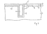
- Figure 6 is a cross section according to Figure 1 for a further embodiment.
- the elements of the embodiment according to Figure 6 that are similar to corresponding elements of the embodiment according to Figure 1 are designated with the same reference numerals.
- the metal layer 7 provided for the through-wafer via has already been structured.
- a mask with a venting feature according to the above description may have been used. This is indicated by the structure of the metal layer 7 shown in Figure 6 , which is similar to the structure of the metal layer 7 shown in Figure 3 .
- a further layer 9 has been applied, which may be a passivation layer, for instance.
- the further layer 9 is to be structured using the mask 3, which may be a resist mask (or a further resist mask).
- the mask 3 is going to be provided with at least one opening 5 at a small distance from the recess or trench 2, as indicated by the dotted vertical lines in Figure 6 .
- the opening 5 has the same venting purpose as the opening 5 of the mask 3 described above in conjunction with Figures 1 to 3 .
- the example shown in Figure 6 is given to indicate how a mask 3 that is provided with a venting feature as described can be applied to various layers in different process steps or repeatedly to different layers in two or more process steps.
- the method enables the use of dry film technology for the masking of high aspect ratio topographies.
- Deep etched features having dimensions or spacings up to 500 ⁇ m covered with a masking resist layer can be processed in low-pressure reactors without the risk of mask rupture and/or delamination. This is accomplished by the use and layout of venting features at the perimeter of the covered structure.
- the geometry is designed in a way that the resist interface just opens in the predefined area under specific subatmospheric pressure conditions to balance detrimental overpressure.
- Dry film technology using a well-known and controllable lamination technique enables high throughput. Only few process parameters have to be controlled. The quality of the dry film mask can be easily controlled at the surface of the wafer and is not affected by the topography. Critical topography is thus easily eliminated by covering deep structures.
Landscapes
- Engineering & Computer Science (AREA)
- Architecture (AREA)
- Structural Engineering (AREA)
- Physics & Mathematics (AREA)
- General Physics & Mathematics (AREA)
- Pressure Sensors (AREA)
- Micromachines (AREA)
- Drying Of Semiconductors (AREA)
Abstract
Description
- This invention relates to the manufacture of semiconductor devices with a high surface topography, in particular for the integration of features like MEMS sensors or TSVs.
-
FR2 823 865-A1 - Mask layers are applied as planar layers continuously covering holes in the substrate or as a lining of sidewalls and bottoms of trenches. Conventional processes for producing the different kinds of mask layers are vacuum-coating and spray-coating, for example. Another method consists of laminating a dry film over the holes, thus forming closed cavities. Gas, especially ambient air, is trapped in the cavities under the environmental conditions prevailing at the time the mask layer is applied. For instance, the gas may have the pressure of an atmosphere under which an etching step is performed. After further process steps the gas pressure in the cavity may exceed the outer pressure, and ruptures in the mask layer may result.
- It is an object of the present invention to disclose a masking method for semiconductor devices with high surface topography, especially a masking method that is suitable for the integration of microelectromechanical sensors or through-wafer vias.
- This object is achieved with the method of producing a semiconductor device according to
claim 1. Embodiments and variants derive from the dependent claims. - The method comprises the steps of providing a semiconductor body or substrate with a recess or trench in a main surface, applying a mask above the main surface, the mask covering the recess or trench, so that the walls and bottom of the recess or trench and the mask together enclose a cavity, which is filled with a gas, and forming at least one opening in the mask at a distance from the recess or trench, the distance being adapted to allow the gas to escape from the cavity via the opening when the difference between the pressure exerted on the mask by the gas and a pressure exerted on the mask from outside the recess or trench is larger than a predefined value.
- In a variant of the method the mask is applied as a dry film using a lamination technique.
- In a further variant of the method the mask forms a planar layer above the recess or trench.
- In further variants of the method the distance is less than 5 µm or even less than 3 µm.
- In a further variant of the method the recess or trench is provided for a through-wafer via or contact comprising a metal layer.
- In a further variant of the method the metal layer is applied to an area of the main surface surrounding the recess or trench, and the mask is used in an etching step to structure the metal layer, so that the opening is transferred to the metal layer.
- In a further variant of the method the opening is locally confined in such a manner that the metal layer extends from the recess or trench beyond the opening.
- In a further variant of the method the metal layer is structured by etching, a further layer is applied, the mask is applied on the further layer, and the mask is used to structure the further layer.
- In a further variant of the method the further layer is a passivation layer, which is also applied in the recess or trench.
- In further variants of the method the gas filling the cavity is captured ambient air or nitrogen.
- In a further variant of the method the opening is one of a plurality of openings formed in the mask at distances from the recess or trench, the distances being adapted to allow the gas to escape from the cavity via at least one of the openings when the difference between the pressure exerted on the mask by the gas and a pressure exerted on the mask from outside the recess or trench is larger than a predefined value.
- The following is a detailed description of examples of the method of producing a semiconductor device.
- Figure 1
- is a cross section of an intermediate product of an example of the method after the application of a mask layer.
- Figure 2
- is a cross section according to
Figure 1 after the formation of mask openings. - Figure 3
- is a cross section according to
Figure 2 of a further intermediate product obtained after the mask has been used to structure a metal layer. - Figure 4
- is a schematic plan view of the arrangement of a recess or trench and mask openings.
- Figure 5
- is a schematic plan view of a further arrangement according to
Figure 4 . - Figure 6
- is a cross section according to
Figure 1 for a further embodiment. -
Figure 1 is a cross section of an intermediate product of an example of the method. A semiconductor body orsubstrate 1 has a recess ortrench 2 in amain surface 10. The recess ortrench 2 can be provided for a through-wafer via or through-substrate via (TSV), for instance. The recess may instead be provided for a microelectromechanical sensor or another integrated component that renders a high topography or high aspect ratio of the substrate surface. If the recess ortrench 2 is provided for a through-substrate via, ametal layer 7 may be applied to form a vertical electrical connection through thesubstrate 1. Themetal layer 7 may cover the sidewall and bottom of the recess ortrench 2 and may extend onto themain surface 10. - A
mask 3 is applied above themain surface 10 as a planar layer, which may be formed from a resist, for instance, and may be produced by a dry film technology. The inner volume of the recess ortrench 2 is thus closed and forms acavity 4, which is filled with the ambient gas that is present when thecavity 4 is being closed. The gas may be ambient air, for example, or the gas may be captured from an artificial atmosphere that is present during a process step immediately preceding the application of themask 3, like a nitrogen atmosphere used during an etching step, for instance. The initial pressure of the gas trapped in thecavity 4 is the same as the outer gas pressure that is prevalent in the moment thecavity 4 is being closed. The gas pressure depends on the temperature and may change during subsequent process steps. - The difference between the pressure exerted on the
mask 3 by the gas trapped in thecavity 4 and a pressure exerted on themask 3 from outside the recess ortrench 2 may change in the further process steps and may in particular increase to values above a predefined value. Thus the pressure difference may exceed a maximal value which is regarded as a tolerable limit. The limit value is predefined according to individual requirements and may especially depend on the mechanical resistance and the adhesive strength of the mask layer. -
Figure 2 is a cross section according toFigure 1 after the formation of at least one opening 5 in themask 3 at a small distance from the recess ortrench 2.Further openings 8 are provided in themask 3 according to the intended structure that is to be produced in a subsequent etching step. The opening 5 near the recess ortrench 2 is provided as a vent to allow the gas to escape from thecavity 4. -
Figure 3 is a cross section according toFigure 2 and shows the device after themask 3 has been used to structure themetal layer 7 and/or further layers not shown in the figures. The size of the opening 5 may be kept small, so that themetal layer 7 can also be removed in the opening 5 without adversely affecting the device structure and the performance of the device during its later operation. The opening 5 is preferably designed in such a way that no wet chemicals like water or developer are able to enter the cavity. The distance 6 between the opening 5 and the recess ortrench 2 may be typically about 2 µm, for instance. In preferred embodiments the distance 6 is less than 5 µm, in particular less than 3 µm. - During the pump down procedure in an RIE (reactive ion etching) process, lowering the external pressure below the pressure of the gas trapped in the
cavity 4, the expansion of the gas that is trapped in thecavity 4 causes themask 3 to be lifted next to the opening 5. Due to the localized lifting of themask 3 from themain surface 10, at least some of the trapped gas escapes through the opening 5, which thus provides a suitable venting feature. In this way the gas pressures inside and outside thecavity 4 are balanced. -
Figure 4 is a schematic plan view of the arrangement of a recess ortrench 2 andmask openings 5, 8. The hidden contours of the recess ortrench 2 and the portion of themetal layer 7 covering the sidewall of the recess ortrench 2 are shown with broken lines surrounding thecavity 4. The opening 5 that is arranged at a small distance 6 from the recess ortrench 2 is provided as a vent of thecavity 4 in the manner described above. Thefurther openings 8 of themask 3 are provided to structure themetal layer 7. Thefurther openings 8 may be larger than shown inFigure 4 , so that themask 3 only covers conductor tracks that are to be left from themetal layer 7 on themain surface 10, for example. -
Figure 5 is a schematic plan view of a further arrangement according toFigure 4 . In the embodiment according toFigure 5 the opening 5 is one of a plurality of openings 5, which are arranged on the periphery of the recess ortrench 2. The sizes, number and arrangement of the openings 5 can be designed according to the requirements of individual embodiments. -
Figure 6 is a cross section according toFigure 1 for a further embodiment. The elements of the embodiment according toFigure 6 that are similar to corresponding elements of the embodiment according toFigure 1 are designated with the same reference numerals. In the process step that is represented inFigure 6 , themetal layer 7 provided for the through-wafer via has already been structured. For the etching step that is performed to structure themetal layer 7, a mask with a venting feature according to the above description may have been used. This is indicated by the structure of themetal layer 7 shown inFigure 6 , which is similar to the structure of themetal layer 7 shown inFigure 3 . A further layer 9 has been applied, which may be a passivation layer, for instance. The further layer 9 is to be structured using themask 3, which may be a resist mask (or a further resist mask). Themask 3 is going to be provided with at least one opening 5 at a small distance from the recess ortrench 2, as indicated by the dotted vertical lines inFigure 6 . The opening 5 has the same venting purpose as the opening 5 of themask 3 described above in conjunction withFigures 1 to 3 . The example shown inFigure 6 is given to indicate how amask 3 that is provided with a venting feature as described can be applied to various layers in different process steps or repeatedly to different layers in two or more process steps. - The method enables the use of dry film technology for the masking of high aspect ratio topographies. Deep etched features having dimensions or spacings up to 500 µm covered with a masking resist layer can be processed in low-pressure reactors without the risk of mask rupture and/or delamination. This is accomplished by the use and layout of venting features at the perimeter of the covered structure. The geometry is designed in a way that the resist interface just opens in the predefined area under specific subatmospheric pressure conditions to balance detrimental overpressure. Dry film technology using a well-known and controllable lamination technique enables high throughput. Only few process parameters have to be controlled. The quality of the dry film mask can be easily controlled at the surface of the wafer and is not affected by the topography. Critical topography is thus easily eliminated by covering deep structures.
-
- 1
- substrate
- 2
- recess or trench
- 3
- mask
- 4
- cavity
- 5
- opening
- 6
- distance
- 7
- metal layer
- 8
- further opening
- 9
- further layer
- 10
- main surface
Claims (13)
- A method of producing a semiconductor device, comprising:- providing a semiconductor body or substrate (1) having a main surface (10) with a recess or trench (2) in the main surface (10), and- applying a mask (3) above the main surface (10), the mask (3) covering the recess or trench (2), so that the recess or trench (2) and the mask (3) form a closed cavity (4), which is filled with a gas,
characterized in that- at least one opening (5) is formed in the mask (3) at a distance (6) from the recess or trench (2), the distance (6) being adapted to allow the gas to escape from the cavity (4) via the opening (5) when the difference between a pressure exerted on the mask (3) by the gas and a pressure exerted on the mask (3) from outside the recess or trench (2) is larger than a predefined value. - The method of claim 1, wherein the mask (3) is applied as a dry film using a lamination technique.
- The method of claim 1 or 2, wherein the mask (3) forms a planar layer above the recess or trench (2).
- The method of one of claims 1 to 3, wherein the distance (6) is less than 5 µm.
- The method of one of claims 1 to 3, wherein the distance (6) is less than 3 µm.
- The method of one of claims 1 to 5, wherein the recess or trench (2) is provided for a through-wafer via or contact comprising a metal layer (7).
- The method of claim 6, wherein
the metal layer (7) is applied to an area of the main surface (10) surrounding the recess or trench (2), and the mask (3) is used in an etching step to structure the metal layer (7), so that the opening (5) is transferred to the metal layer (7). - The method of claim 7, wherein
the opening (5) is locally confined in such a manner that the metal layer (7) extends from the recess or trench (2) beyond the opening (5). - The method of claim 6, wherein
the metal layer (7) is structured by etching,
a further layer (9) is applied,
the mask (3) is applied on the further layer (9), and the mask (3) is used to structure the further layer (9). - The method of claim 9, wherein
the further layer (9) is a passivation layer, which is also applied in the recess or trench (2). - The method of one of claims 1 to 10, wherein the gas filling the cavity (4) is captured ambient air.
- The method of one of claims 1 to 10, wherein the gas filling the cavity (4) is nitrogen.
- The method of one of claims 1 to 12, wherein the opening (5) is one of a plurality of openings (5) formed in the mask (3) at distances (6) from the recess or trench (2), the distances (6) being adapted to allow the gas to escape from the cavity (4) via at least one of the openings (5) when the difference between a pressure exerted on the mask (3) by the gas and a pressure exerted on the mask (3) from outside the recess or trench (2) is larger than a predefined value.
Priority Applications (3)
| Application Number | Priority Date | Filing Date | Title |
|---|---|---|---|
| EP13154625.1A EP2765456B1 (en) | 2013-02-08 | 2013-02-08 | Masking method for semiconductor devices with high surface topography |
| PCT/EP2014/051715 WO2014122055A1 (en) | 2013-02-08 | 2014-01-29 | Masking method for semiconductor devices with high surface topography |
| US14/766,412 US9466529B2 (en) | 2013-02-08 | 2014-01-29 | Masking method for semiconductor devices with high surface topography |
Applications Claiming Priority (1)
| Application Number | Priority Date | Filing Date | Title |
|---|---|---|---|
| EP13154625.1A EP2765456B1 (en) | 2013-02-08 | 2013-02-08 | Masking method for semiconductor devices with high surface topography |
Publications (2)
| Publication Number | Publication Date |
|---|---|
| EP2765456A1 true EP2765456A1 (en) | 2014-08-13 |
| EP2765456B1 EP2765456B1 (en) | 2016-05-04 |
Family
ID=47832895
Family Applications (1)
| Application Number | Title | Priority Date | Filing Date |
|---|---|---|---|
| EP13154625.1A Not-in-force EP2765456B1 (en) | 2013-02-08 | 2013-02-08 | Masking method for semiconductor devices with high surface topography |
Country Status (3)
| Country | Link |
|---|---|
| US (1) | US9466529B2 (en) |
| EP (1) | EP2765456B1 (en) |
| WO (1) | WO2014122055A1 (en) |
Families Citing this family (1)
| Publication number | Priority date | Publication date | Assignee | Title |
|---|---|---|---|---|
| US20230096301A1 (en) * | 2021-09-29 | 2023-03-30 | Catlam, Llc. | Circuit Board Traces in Channels using Electroless and Electroplated Depositions |
Citations (3)
| Publication number | Priority date | Publication date | Assignee | Title |
|---|---|---|---|---|
| FR2823865A1 (en) | 2001-09-20 | 2002-10-25 | Commissariat Energie Atomique | METHOD FOR SURFACE LITHOGRAPHY OF A SUBSTRATE WITH HIGH TOPOLOGY |
| EP1353364A2 (en) * | 1997-10-22 | 2003-10-15 | Interuniversitair Micro-Elektronica Centrum Vzw | Anisotropic etching of organic-containing insulating layers |
| US20100330504A1 (en) * | 2008-01-30 | 2010-12-30 | Munetoshi Irisawa | Method for electroconductive pattern formation |
Family Cites Families (1)
| Publication number | Priority date | Publication date | Assignee | Title |
|---|---|---|---|---|
| US6265139B1 (en) * | 1998-12-30 | 2001-07-24 | Samsung Electro-Mechanics Co., Ltd. | Method for fabricating piezoelectric/electrostrictive ceramic micro actuator using photolithography |
-
2013
- 2013-02-08 EP EP13154625.1A patent/EP2765456B1/en not_active Not-in-force
-
2014
- 2014-01-29 US US14/766,412 patent/US9466529B2/en active Active
- 2014-01-29 WO PCT/EP2014/051715 patent/WO2014122055A1/en not_active Ceased
Patent Citations (3)
| Publication number | Priority date | Publication date | Assignee | Title |
|---|---|---|---|---|
| EP1353364A2 (en) * | 1997-10-22 | 2003-10-15 | Interuniversitair Micro-Elektronica Centrum Vzw | Anisotropic etching of organic-containing insulating layers |
| FR2823865A1 (en) | 2001-09-20 | 2002-10-25 | Commissariat Energie Atomique | METHOD FOR SURFACE LITHOGRAPHY OF A SUBSTRATE WITH HIGH TOPOLOGY |
| US20100330504A1 (en) * | 2008-01-30 | 2010-12-30 | Munetoshi Irisawa | Method for electroconductive pattern formation |
Non-Patent Citations (1)
| Title |
|---|
| SPIERING V L ET AL: "PLANARIZATION AND FABRICATION OF BRIDGES ACROSS DEEP GROOVES OR HOLES IN SILICON USING A DRY FILM PHOTORESIST FOLLOWED BY AN ETCH BACK", JOURNAL OF MICROMECHANICS & MICROENGINEERING, INSTITUTE OF PHYSICS PUBLISHING, BRISTOL, GB, vol. 5, no. 2, 5 September 1994 (1994-09-05), pages 189 - 192, XP008003984, ISSN: 0960-1317, DOI: 10.1088/0960-1317/5/2/036 * |
Also Published As
| Publication number | Publication date |
|---|---|
| US9466529B2 (en) | 2016-10-11 |
| US20150380308A1 (en) | 2015-12-31 |
| EP2765456B1 (en) | 2016-05-04 |
| WO2014122055A1 (en) | 2014-08-14 |
Similar Documents
| Publication | Publication Date | Title |
|---|---|---|
| CN102194777B (en) | Chip package and method of forming the same | |
| US8093119B2 (en) | CMOS microelectromechanical system (MEMS) device and fabrication method thereof | |
| US8148790B2 (en) | Thin-film lid MEMS devices and methods | |
| US8587078B2 (en) | Integrated circuit and fabricating method thereof | |
| KR102202821B1 (en) | Method for forming multi-depth mems package | |
| US20150132880A1 (en) | Microelectromechanical system (mems) device and fabrication method thereof | |
| US9187320B2 (en) | Method for etching a complex pattern | |
| US20140015069A1 (en) | MEMS Devices, Packaged MEMS Devices, and Methods of Manufacture Thereof | |
| US8252695B2 (en) | Method for manufacturing a micro-electromechanical structure | |
| US8980698B2 (en) | MEMS devices | |
| EP2897170B1 (en) | CMOS integrated method for fabrication of thermopile pixel on semiconductor substrate with buried insulation regions | |
| EP3119533B1 (en) | Cmut device and manufacturing method | |
| EP2327658B1 (en) | Method for manufacturing microelectronic devices and devices according to such method | |
| TWI418002B (en) | Chip package and method of manufacturing same | |
| CN102328899A (en) | Method for manufacturing cavities of different depths | |
| US8329492B2 (en) | Micro electronic device and method for fabricating micro electromechanical system resonator thereof | |
| US7829364B2 (en) | Method of fabricating a suspension microstructure | |
| US9466529B2 (en) | Masking method for semiconductor devices with high surface topography | |
| TWI530449B (en) | Mixed mode mems chip and manufacturing method thereof | |
| JP2007514557A (en) | Microparts with sealed cavities and plugs and methods for producing such microparts | |
| EP3682210B1 (en) | Capacitive pressure sensors and other devices having a suspended membrane and having rounded corners at an anchor edge | |
| US20180170748A1 (en) | Semiconductor devices with cavities and methods for fabricating semiconductor devices with cavities | |
| CN116946966A (en) | MEMS device and manufacturing method thereof | |
| EP3181514B1 (en) | Microelectromechanical device and method for manufacturing it | |
| CN107799386B (en) | Semiconductor device and method for manufacturing the same |
Legal Events
| Date | Code | Title | Description |
|---|---|---|---|
| PUAI | Public reference made under article 153(3) epc to a published international application that has entered the european phase |
Free format text: ORIGINAL CODE: 0009012 |
|
| 17P | Request for examination filed |
Effective date: 20130208 |
|
| AK | Designated contracting states |
Kind code of ref document: A1 Designated state(s): AL AT BE BG CH CY CZ DE DK EE ES FI FR GB GR HR HU IE IS IT LI LT LU LV MC MK MT NL NO PL PT RO RS SE SI SK SM TR |
|
| AX | Request for extension of the european patent |
Extension state: BA ME |
|
| R17P | Request for examination filed (corrected) |
Effective date: 20140923 |
|
| RBV | Designated contracting states (corrected) |
Designated state(s): AL AT BE BG CH CY CZ DE DK EE ES FI FR GB GR HR HU IE IS IT LI LT LU LV MC MK MT NL NO PL PT RO RS SE SI SK SM TR |
|
| GRAP | Despatch of communication of intention to grant a patent |
Free format text: ORIGINAL CODE: EPIDOSNIGR1 |
|
| INTG | Intention to grant announced |
Effective date: 20151201 |
|
| GRAS | Grant fee paid |
Free format text: ORIGINAL CODE: EPIDOSNIGR3 |
|
| GRAA | (expected) grant |
Free format text: ORIGINAL CODE: 0009210 |
|
| RIN1 | Information on inventor provided before grant (corrected) |
Inventor name: KOPPITSCH, GUENTHER Inventor name: STUECKLER, EWALD Inventor name: TEVA, JORDI Inventor name: ROHRACHER, KARL |
|
| AK | Designated contracting states |
Kind code of ref document: B1 Designated state(s): AL AT BE BG CH CY CZ DE DK EE ES FI FR GB GR HR HU IE IS IT LI LT LU LV MC MK MT NL NO PL PT RO RS SE SI SK SM TR |
|
| REG | Reference to a national code |
Ref country code: GB Ref legal event code: FG4D |
|
| REG | Reference to a national code |
Ref country code: CH Ref legal event code: EP |
|
| REG | Reference to a national code |
Ref country code: AT Ref legal event code: REF Ref document number: 797424 Country of ref document: AT Kind code of ref document: T Effective date: 20160515 |
|
| REG | Reference to a national code |
Ref country code: IE Ref legal event code: FG4D |
|
| REG | Reference to a national code |
Ref country code: DE Ref legal event code: R096 Ref document number: 602013007203 Country of ref document: DE |
|
| REG | Reference to a national code |
Ref country code: NL Ref legal event code: MP Effective date: 20160504 |
|
| REG | Reference to a national code |
Ref country code: LT Ref legal event code: MG4D |
|
| PG25 | Lapsed in a contracting state [announced via postgrant information from national office to epo] |
Ref country code: LT Free format text: LAPSE BECAUSE OF FAILURE TO SUBMIT A TRANSLATION OF THE DESCRIPTION OR TO PAY THE FEE WITHIN THE PRESCRIBED TIME-LIMIT Effective date: 20160504 Ref country code: NO Free format text: LAPSE BECAUSE OF FAILURE TO SUBMIT A TRANSLATION OF THE DESCRIPTION OR TO PAY THE FEE WITHIN THE PRESCRIBED TIME-LIMIT Effective date: 20160804 Ref country code: NL Free format text: LAPSE BECAUSE OF FAILURE TO SUBMIT A TRANSLATION OF THE DESCRIPTION OR TO PAY THE FEE WITHIN THE PRESCRIBED TIME-LIMIT Effective date: 20160504 Ref country code: FI Free format text: LAPSE BECAUSE OF FAILURE TO SUBMIT A TRANSLATION OF THE DESCRIPTION OR TO PAY THE FEE WITHIN THE PRESCRIBED TIME-LIMIT Effective date: 20160504 |
|
| REG | Reference to a national code |
Ref country code: AT Ref legal event code: MK05 Ref document number: 797424 Country of ref document: AT Kind code of ref document: T Effective date: 20160504 |
|
| PG25 | Lapsed in a contracting state [announced via postgrant information from national office to epo] |
Ref country code: RS Free format text: LAPSE BECAUSE OF FAILURE TO SUBMIT A TRANSLATION OF THE DESCRIPTION OR TO PAY THE FEE WITHIN THE PRESCRIBED TIME-LIMIT Effective date: 20160504 Ref country code: SE Free format text: LAPSE BECAUSE OF FAILURE TO SUBMIT A TRANSLATION OF THE DESCRIPTION OR TO PAY THE FEE WITHIN THE PRESCRIBED TIME-LIMIT Effective date: 20160504 Ref country code: ES Free format text: LAPSE BECAUSE OF FAILURE TO SUBMIT A TRANSLATION OF THE DESCRIPTION OR TO PAY THE FEE WITHIN THE PRESCRIBED TIME-LIMIT Effective date: 20160504 Ref country code: PT Free format text: LAPSE BECAUSE OF FAILURE TO SUBMIT A TRANSLATION OF THE DESCRIPTION OR TO PAY THE FEE WITHIN THE PRESCRIBED TIME-LIMIT Effective date: 20160905 Ref country code: HR Free format text: LAPSE BECAUSE OF FAILURE TO SUBMIT A TRANSLATION OF THE DESCRIPTION OR TO PAY THE FEE WITHIN THE PRESCRIBED TIME-LIMIT Effective date: 20160504 Ref country code: GR Free format text: LAPSE BECAUSE OF FAILURE TO SUBMIT A TRANSLATION OF THE DESCRIPTION OR TO PAY THE FEE WITHIN THE PRESCRIBED TIME-LIMIT Effective date: 20160805 Ref country code: LV Free format text: LAPSE BECAUSE OF FAILURE TO SUBMIT A TRANSLATION OF THE DESCRIPTION OR TO PAY THE FEE WITHIN THE PRESCRIBED TIME-LIMIT Effective date: 20160504 |
|
| PG25 | Lapsed in a contracting state [announced via postgrant information from national office to epo] |
Ref country code: IT Free format text: LAPSE BECAUSE OF FAILURE TO SUBMIT A TRANSLATION OF THE DESCRIPTION OR TO PAY THE FEE WITHIN THE PRESCRIBED TIME-LIMIT Effective date: 20160504 |
|
| PG25 | Lapsed in a contracting state [announced via postgrant information from national office to epo] |
Ref country code: DK Free format text: LAPSE BECAUSE OF FAILURE TO SUBMIT A TRANSLATION OF THE DESCRIPTION OR TO PAY THE FEE WITHIN THE PRESCRIBED TIME-LIMIT Effective date: 20160504 Ref country code: EE Free format text: LAPSE BECAUSE OF FAILURE TO SUBMIT A TRANSLATION OF THE DESCRIPTION OR TO PAY THE FEE WITHIN THE PRESCRIBED TIME-LIMIT Effective date: 20160504 Ref country code: SK Free format text: LAPSE BECAUSE OF FAILURE TO SUBMIT A TRANSLATION OF THE DESCRIPTION OR TO PAY THE FEE WITHIN THE PRESCRIBED TIME-LIMIT Effective date: 20160504 Ref country code: CZ Free format text: LAPSE BECAUSE OF FAILURE TO SUBMIT A TRANSLATION OF THE DESCRIPTION OR TO PAY THE FEE WITHIN THE PRESCRIBED TIME-LIMIT Effective date: 20160504 Ref country code: RO Free format text: LAPSE BECAUSE OF FAILURE TO SUBMIT A TRANSLATION OF THE DESCRIPTION OR TO PAY THE FEE WITHIN THE PRESCRIBED TIME-LIMIT Effective date: 20160504 |
|
| REG | Reference to a national code |
Ref country code: DE Ref legal event code: R097 Ref document number: 602013007203 Country of ref document: DE |
|
| PG25 | Lapsed in a contracting state [announced via postgrant information from national office to epo] |
Ref country code: BE Free format text: LAPSE BECAUSE OF FAILURE TO SUBMIT A TRANSLATION OF THE DESCRIPTION OR TO PAY THE FEE WITHIN THE PRESCRIBED TIME-LIMIT Effective date: 20160504 Ref country code: AT Free format text: LAPSE BECAUSE OF FAILURE TO SUBMIT A TRANSLATION OF THE DESCRIPTION OR TO PAY THE FEE WITHIN THE PRESCRIBED TIME-LIMIT Effective date: 20160504 Ref country code: SM Free format text: LAPSE BECAUSE OF FAILURE TO SUBMIT A TRANSLATION OF THE DESCRIPTION OR TO PAY THE FEE WITHIN THE PRESCRIBED TIME-LIMIT Effective date: 20160504 Ref country code: PL Free format text: LAPSE BECAUSE OF FAILURE TO SUBMIT A TRANSLATION OF THE DESCRIPTION OR TO PAY THE FEE WITHIN THE PRESCRIBED TIME-LIMIT Effective date: 20160504 |
|
| PLBE | No opposition filed within time limit |
Free format text: ORIGINAL CODE: 0009261 |
|
| STAA | Information on the status of an ep patent application or granted ep patent |
Free format text: STATUS: NO OPPOSITION FILED WITHIN TIME LIMIT |
|
| 26N | No opposition filed |
Effective date: 20170207 |
|
| PG25 | Lapsed in a contracting state [announced via postgrant information from national office to epo] |
Ref country code: SI Free format text: LAPSE BECAUSE OF FAILURE TO SUBMIT A TRANSLATION OF THE DESCRIPTION OR TO PAY THE FEE WITHIN THE PRESCRIBED TIME-LIMIT Effective date: 20160504 |
|
| PG25 | Lapsed in a contracting state [announced via postgrant information from national office to epo] |
Ref country code: MC Free format text: LAPSE BECAUSE OF FAILURE TO SUBMIT A TRANSLATION OF THE DESCRIPTION OR TO PAY THE FEE WITHIN THE PRESCRIBED TIME-LIMIT Effective date: 20160504 |
|
| REG | Reference to a national code |
Ref country code: CH Ref legal event code: PL |
|
| GBPC | Gb: european patent ceased through non-payment of renewal fee |
Effective date: 20170208 |
|
| PG25 | Lapsed in a contracting state [announced via postgrant information from national office to epo] |
Ref country code: LI Free format text: LAPSE BECAUSE OF NON-PAYMENT OF DUE FEES Effective date: 20170228 Ref country code: CH Free format text: LAPSE BECAUSE OF NON-PAYMENT OF DUE FEES Effective date: 20170228 |
|
| REG | Reference to a national code |
Ref country code: IE Ref legal event code: MM4A |
|
| REG | Reference to a national code |
Ref country code: FR Ref legal event code: ST Effective date: 20171031 |
|
| PG25 | Lapsed in a contracting state [announced via postgrant information from national office to epo] |
Ref country code: LU Free format text: LAPSE BECAUSE OF NON-PAYMENT OF DUE FEES Effective date: 20170208 |
|
| PG25 | Lapsed in a contracting state [announced via postgrant information from national office to epo] |
Ref country code: FR Free format text: LAPSE BECAUSE OF NON-PAYMENT OF DUE FEES Effective date: 20170228 |
|
| PG25 | Lapsed in a contracting state [announced via postgrant information from national office to epo] |
Ref country code: IE Free format text: LAPSE BECAUSE OF NON-PAYMENT OF DUE FEES Effective date: 20170208 Ref country code: GB Free format text: LAPSE BECAUSE OF NON-PAYMENT OF DUE FEES Effective date: 20170208 |
|
| PG25 | Lapsed in a contracting state [announced via postgrant information from national office to epo] |
Ref country code: MT Free format text: LAPSE BECAUSE OF NON-PAYMENT OF DUE FEES Effective date: 20170208 |
|
| PG25 | Lapsed in a contracting state [announced via postgrant information from national office to epo] |
Ref country code: AL Free format text: LAPSE BECAUSE OF FAILURE TO SUBMIT A TRANSLATION OF THE DESCRIPTION OR TO PAY THE FEE WITHIN THE PRESCRIBED TIME-LIMIT Effective date: 20160504 |
|
| PG25 | Lapsed in a contracting state [announced via postgrant information from national office to epo] |
Ref country code: HU Free format text: LAPSE BECAUSE OF FAILURE TO SUBMIT A TRANSLATION OF THE DESCRIPTION OR TO PAY THE FEE WITHIN THE PRESCRIBED TIME-LIMIT; INVALID AB INITIO Effective date: 20130208 |
|
| PG25 | Lapsed in a contracting state [announced via postgrant information from national office to epo] |
Ref country code: BG Free format text: LAPSE BECAUSE OF FAILURE TO SUBMIT A TRANSLATION OF THE DESCRIPTION OR TO PAY THE FEE WITHIN THE PRESCRIBED TIME-LIMIT Effective date: 20160504 |
|
| PG25 | Lapsed in a contracting state [announced via postgrant information from national office to epo] |
Ref country code: CY Free format text: LAPSE BECAUSE OF NON-PAYMENT OF DUE FEES Effective date: 20160504 |
|
| PG25 | Lapsed in a contracting state [announced via postgrant information from national office to epo] |
Ref country code: MK Free format text: LAPSE BECAUSE OF FAILURE TO SUBMIT A TRANSLATION OF THE DESCRIPTION OR TO PAY THE FEE WITHIN THE PRESCRIBED TIME-LIMIT Effective date: 20160504 |
|
| PG25 | Lapsed in a contracting state [announced via postgrant information from national office to epo] |
Ref country code: TR Free format text: LAPSE BECAUSE OF FAILURE TO SUBMIT A TRANSLATION OF THE DESCRIPTION OR TO PAY THE FEE WITHIN THE PRESCRIBED TIME-LIMIT Effective date: 20160504 |
|
| PG25 | Lapsed in a contracting state [announced via postgrant information from national office to epo] |
Ref country code: IS Free format text: LAPSE BECAUSE OF FAILURE TO SUBMIT A TRANSLATION OF THE DESCRIPTION OR TO PAY THE FEE WITHIN THE PRESCRIBED TIME-LIMIT Effective date: 20160904 |
|
| P01 | Opt-out of the competence of the unified patent court (upc) registered |
Effective date: 20230822 |
|
| PGFP | Annual fee paid to national office [announced via postgrant information from national office to epo] |
Ref country code: DE Payment date: 20240219 Year of fee payment: 12 |
|
| REG | Reference to a national code |
Ref country code: DE Ref legal event code: R119 Ref document number: 602013007203 Country of ref document: DE |
|
| PG25 | Lapsed in a contracting state [announced via postgrant information from national office to epo] |
Ref country code: DE Free format text: LAPSE BECAUSE OF NON-PAYMENT OF DUE FEES Effective date: 20250902 |