EP2763184A1 - Inks for the in-situ production of chalcogens and/or chalcogenides that form semiconductor layers, production method thereof and use of same - Google Patents
Inks for the in-situ production of chalcogens and/or chalcogenides that form semiconductor layers, production method thereof and use of same Download PDFInfo
- Publication number
- EP2763184A1 EP2763184A1 EP12836775.2A EP12836775A EP2763184A1 EP 2763184 A1 EP2763184 A1 EP 2763184A1 EP 12836775 A EP12836775 A EP 12836775A EP 2763184 A1 EP2763184 A1 EP 2763184A1
- Authority
- EP
- European Patent Office
- Prior art keywords
- group
- ink
- metal element
- solution
- seo
- Prior art date
- Legal status (The legal status is an assumption and is not a legal conclusion. Google has not performed a legal analysis and makes no representation as to the accuracy of the status listed.)
- Withdrawn
Links
Images

Classifications
-
- H—ELECTRICITY
- H10—SEMICONDUCTOR DEVICES; ELECTRIC SOLID-STATE DEVICES NOT OTHERWISE PROVIDED FOR
- H10F—INORGANIC SEMICONDUCTOR DEVICES SENSITIVE TO INFRARED RADIATION, LIGHT, ELECTROMAGNETIC RADIATION OF SHORTER WAVELENGTH OR CORPUSCULAR RADIATION
- H10F77/00—Constructional details of devices covered by this subclass
- H10F77/10—Semiconductor bodies
- H10F77/12—Active materials
- H10F77/126—Active materials comprising only Group I-III-VI chalcopyrite materials, e.g. CuInSe2, CuGaSe2 or CuInGaSe2 [CIGS]
-
- H—ELECTRICITY
- H10—SEMICONDUCTOR DEVICES; ELECTRIC SOLID-STATE DEVICES NOT OTHERWISE PROVIDED FOR
- H10F—INORGANIC SEMICONDUCTOR DEVICES SENSITIVE TO INFRARED RADIATION, LIGHT, ELECTROMAGNETIC RADIATION OF SHORTER WAVELENGTH OR CORPUSCULAR RADIATION
- H10F77/00—Constructional details of devices covered by this subclass
- H10F77/10—Semiconductor bodies
- H10F77/12—Active materials
-
- H—ELECTRICITY
- H10—SEMICONDUCTOR DEVICES; ELECTRIC SOLID-STATE DEVICES NOT OTHERWISE PROVIDED FOR
- H10P—GENERIC PROCESSES OR APPARATUS FOR THE MANUFACTURE OR TREATMENT OF DEVICES COVERED BY CLASS H10
- H10P14/00—Formation of materials, e.g. in the shape of layers or pillars
- H10P14/20—Formation of materials, e.g. in the shape of layers or pillars of semiconductor materials
- H10P14/26—Formation of materials, e.g. in the shape of layers or pillars of semiconductor materials using liquid deposition
- H10P14/265—Formation of materials, e.g. in the shape of layers or pillars of semiconductor materials using liquid deposition using solutions
-
- H—ELECTRICITY
- H10—SEMICONDUCTOR DEVICES; ELECTRIC SOLID-STATE DEVICES NOT OTHERWISE PROVIDED FOR
- H10P—GENERIC PROCESSES OR APPARATUS FOR THE MANUFACTURE OR TREATMENT OF DEVICES COVERED BY CLASS H10
- H10P14/00—Formation of materials, e.g. in the shape of layers or pillars
- H10P14/20—Formation of materials, e.g. in the shape of layers or pillars of semiconductor materials
- H10P14/34—Deposited materials, e.g. layers
- H10P14/3402—Deposited materials, e.g. layers characterised by the chemical composition
- H10P14/3436—Deposited materials, e.g. layers characterised by the chemical composition being chalcogenide semiconductor materials not being oxides, e.g. ternary compounds
-
- Y—GENERAL TAGGING OF NEW TECHNOLOGICAL DEVELOPMENTS; GENERAL TAGGING OF CROSS-SECTIONAL TECHNOLOGIES SPANNING OVER SEVERAL SECTIONS OF THE IPC; TECHNICAL SUBJECTS COVERED BY FORMER USPC CROSS-REFERENCE ART COLLECTIONS [XRACs] AND DIGESTS
- Y02—TECHNOLOGIES OR APPLICATIONS FOR MITIGATION OR ADAPTATION AGAINST CLIMATE CHANGE
- Y02E—REDUCTION OF GREENHOUSE GAS [GHG] EMISSIONS, RELATED TO ENERGY GENERATION, TRANSMISSION OR DISTRIBUTION
- Y02E10/00—Energy generation through renewable energy sources
- Y02E10/50—Photovoltaic [PV] energy
- Y02E10/541—CuInSe2 material PV cells
-
- Y—GENERAL TAGGING OF NEW TECHNOLOGICAL DEVELOPMENTS; GENERAL TAGGING OF CROSS-SECTIONAL TECHNOLOGIES SPANNING OVER SEVERAL SECTIONS OF THE IPC; TECHNICAL SUBJECTS COVERED BY FORMER USPC CROSS-REFERENCE ART COLLECTIONS [XRACs] AND DIGESTS
- Y02—TECHNOLOGIES OR APPLICATIONS FOR MITIGATION OR ADAPTATION AGAINST CLIMATE CHANGE
- Y02P—CLIMATE CHANGE MITIGATION TECHNOLOGIES IN THE PRODUCTION OR PROCESSING OF GOODS
- Y02P70/00—Climate change mitigation technologies in the production process for final industrial or consumer products
- Y02P70/50—Manufacturing or production processes characterised by the final manufactured product
Definitions
- the present invention relates to ink compositions used for printing layers of compounds, mainly of selenium, known for their semiconductor properties. Of particular interest is their use in the mass production of low-cost photovoltaic devices.
- Thin layer photovoltaic materials for example chalcopyrites of the Cu(In,Ga)Se 2 (CIGS) type, are promising candidates for large-scale future production due to their high photoelectric efficiency, reaching 20 %, and excellent stability.
- CGS Cu(In,Ga)Se 2
- compositions containing selenium dioxide and/or selenites which have been reduced in-situ by means of further processing.
- compositions based on solutions whose viscosity is increased by adding cellulose derivatives have been described ( US2008/044570 ), as well as oxide nanoparticle suspensions ( EP1870943 ) and chalcogenides ( WO2007/065096 , US2007/054435 , US2007/169811 ).
- Cu(In,Ga)Se 2 Apart from Cu(In,Ga)Se 2 , there are many promising thin layer materials for use in selenium-based photovoltaic and electronic devices. Layers of elemental selenium may also be used in intermediate steps in the manufacture of Cu(In,Ga)Se 2 absorbers ( F. Hergert et al., Journal of Physics and Chemistry of Solids 66 (2005, 1903 ) or other materials.
- the present invention relates to ink compositions used for printing layers preferably containing selenium dioxide and/or metallic selenites, which are then converted into selenium and/or selenides.
- the invention is based on the in-situ reduction reaction of selenium dioxide and/or metallic selenites in order to form elemental selenium or selenides.
- This reaction may be carried out in the presence of an organic additive in the composition, such as triethanolamine, for example.
- an organic additive in the composition such as triethanolamine, for example.
- layers of selenium are obtained from the printed layers: 32 SeO 2 + 2 C 6 H 15 NO 3 ⁇ 32 Se + 30 CO 2 + 24 H 2 O + N 2 (I) or selenides.
- selenites may have been previously produced by means of the reaction of a soluble selenite (or tellurite), for example sodium selenite, with soluble salt or salts of the ion or ions to be used: 3 SeO 3 2- + 2 Me 3+ ⁇ Me 2 (SeO 3 ) 3 (IIIa) SeO 3 2- + Me 2+ ⁇ MeSeO 3 (IIIb)
- the present invention therefore relates to ink compositions for printing, that make it possible to print layers of selenides and other chalcogenides with a very uniform composition without the need for polymeric additives to facilitate homogeneous printing.
- the obtained layers may be processed in an inert atmosphere, without the need to use toxic gasses, so as to produce, in the case of gallium, layers with excellent incorporation of all the metals present.
- the invention relates to the way in which these compositions are made to react with each other, in-situ, to give rise to the desired semiconductor.
- a first object of the present invention is an ink composition for the in-situ production of chalcogens and/or chalcogenides characterised in that it comprises at least one chalcogenite compound having a formula selected from a group consisting of SeO 2 , M(SO 3 ) n , M(SeO 3 ) n and M(TeO 3 ) n , wherein 0.5 ⁇ n ⁇ 2 and M is a metal element, preferably selected from the group Cu, In and Ga.
- the chalcogenite consists of selenite.
- an object of the present invention is an ink for the in-situ production of chalcogens and/or chalcogenides consisting of a suspension or solution of said composition, as well as the use of said ink for the in-situ preparation of semiconductor materials by printing or depositing them in layers and the formation of chalcogens and/or chalcogenides from the compounds in the ink.
- an object of the invention is a method for preparing said ink.
- said method is characterised it that it comprises mixing:
- This mixture is heated while stirring at a temperature preferably comprised between 0°C and 100°C until dissolving, said solution constituting the ink to be used.
- the addition or modification of the chalcogen element content may optionally be carried out through processing in atmospheres containing vapours of said elements.
- the production method of the inks may comprise:
- this method may comprise the previous preparation of the chalcogenite compound by adding, in a suitable receptacle, over a suspension containing the acid or oxide of the selected chalcogen element, preferably selenium, an equimolecular amount of hydroxide solution, preferably sodium hydroxide, and the amount of water which is enough to reach a concentration of chalcogen between 1 mM and 2 M.
- the selected chalcogen element preferably selenium
- an equimolecular amount of hydroxide solution preferably sodium hydroxide
- the oxide may consist of selenium or tellurium dioxide, as well as other selenium or tellurium and oxygen derivatives.
- other alternative elements such as P, As, I, Br and Cl may be taken into account.
- the chalcogenide object of the method may contain one or more of the following elements: Sn, Zn, Cd, Sb, Ag, Au, Al, Na, K, Mg, Ca, Sr, Ba, B, V, Ti, Zr, Ge, Si, Pb, Tl, Ni, Co, Fe, Hg, V, Nb, Mn and/or Cr.
- step (e) it is possible to add at least one compound selected among organic compounds which do or do not have shimmering, binding, surfactant, wetting, levelling, degassing or viscosity modifying effects, as well as inorganic or organic solvents such as, though not limited to, alcohols and amines.
- the composition may also comprise solid nanoparticles of the aforementioned metals or their compounds such as, though not limited to, selenites.
- Said nanoparticles may be prepared from soluble salts giving rise to precipitation with a solution of sodium selenite ( L. Vlaev and G. Gospodinov, Termochimica Acta 370 (2001), 15).
- the resulting product subjected to thermal processing, releases SeO 2 and metal oxides.
- the nanoparticles have smaller dimensions than the thickness of the layer, said dimensions preferably being between 2 to 3,000 nm.
- an object of the invention is the use of the ink obtained from the described methods for the in-situ production of chalcogens and/or chalcogenides that give rise to layers of semiconductors.
- the ink is first distributed or deposited on the surface to be processed, preferably a glass substrate coated with molybdenum, although other substrates such as metal, ceramic, polymer or combinations thereof may be used.
- the ink is deposited forming layers of liquid thickness between 1 to 100 ⁇ m.
- the substrate and deposited layer are together subjected to thermal processing at least once.
- thermal processing twice: first, slow thermal processing, preferably between 80 °C to 400 °C, in controlled air or atmosphere and, subsequently, rapid thermal processing, preferably between 80 °C to 1,200°C in a controlled atmosphere, thus obtaining a semiconductor layer.
- Said thermal processing may be carried out in a furnace, on a hot plate or by infrared lighting.
- the obtained semiconductor layer consists of an oxygen-free chalcogenide layer, with semiconductor characteristics, that may preferably be used for producing solar panels.
- Deposition over conductive substrates and, especially, over insulating substrates coated with conductive layers, is of particular interest for photovoltaic applications.
- the composition of selenides may be printed over glass substrates coated with molybdenum, using a system allowing for the production of a layer approximately 50 microns thick before drying.
- the assembly is placed over a heating plate at 350 °C for a time period preferably between 0.5 s to 1 h.
- said method is repeated, accumulating several layers until reaching the desired thickness (for example, between 100 nanometres to 50 micrometres) and then it is subjected to final thermal processing, preferably rapid thermal processing with a heating speed of between 100 to 500 °C/min up to 550-600 °C.
- a photovoltaic device may be produced from the panels whose production has been described, by depositing on top of said layer, another layer of an n-type semiconductor, preferably consisting of a compound of at least one metal from the group Cd, Zn or In, and a clear conductive layer containing oxide or a mixture of oxides of at least one metal selected from the group Zn, Al, In, Sn, Sb and Cd.
- an n-type semiconductor preferably consisting of a compound of at least one metal from the group Cd, Zn or In
- a clear conductive layer containing oxide or a mixture of oxides of at least one metal selected from the group Zn, Al, In, Sn, Sb and Cd.
- This method uses the precipitation of nanoparticles of Cu, In and Ga selenides, taking advantage of their low solubility, and describes their use in ink to deposit layers of Cu(In,Ga)Se 2 .
- Sulphates have been used as metal anions, although other soluble salts, such as nitrates, chlorides, acetates, iodides, bromides, etc. may be used:
- Example 1 Composition containing selenium dioxide and use thereof for printing layers of selenium.
- Example 2 Composition containing nanoparticled Cu, In and Ga selenites and use thereof for printing Cu(In,Ga)Se 2 .
- Solution A was added dropwise to solution B until a pH of 3-7 was reached.
- the precipitate was filtered and washed with ethanol.
- the obtained powder was dispersed in ethanol and triethanolamine was added to the suspension.
- the composition thus obtained was deposited on a glass substrate coated with molybdenum using two 50 ⁇ m thick pieces of adhesive tape, attached in parallel on the substrate, and sliding a glass rod over them; the excess of the suspension was removed from the layer.
- the test piece thus obtained was placed on an electric plate at 350 °C for 2 minutes and then was subjected to rapid thermal processing using halogen radiation at a heating speed of 500 °C/min up to 550 °C.
- the thickness of the layer was approximately 3 ⁇ m ( Figure 4 ).
- Example 3 Manufacture of a photovoltaic device according to the present invention.
- the current-voltage characteristic of a 0.1 cm 2 area was measured under simulated solar illumination. Efficiencies of 7.24 % were recorded with an open circuit voltage of 450 mV, a short circuit current of 26 mA/cm 2 and fill factor of 62 % ( Figure 5 ). Furthermore, in some isolated tests, the voltage increased to 460 mV, and the efficiency to 7.5 %.
Landscapes
- Photovoltaic Devices (AREA)
- Inks, Pencil-Leads, Or Crayons (AREA)
Abstract
Description
- The present invention relates to ink compositions used for printing layers of compounds, mainly of selenium, known for their semiconductor properties. Of particular interest is their use in the mass production of low-cost photovoltaic devices.
- The environmental consequences of fossil fuels usage and the economic repercussion associated with their depletion has made the introduction of renewable and clean energy sources an absolute necessity. The sun is a feasible source to satisfy our energy needs. The only limitation to large-scale photoelectric conversion that is sufficient for global consumption is the high cost and low production volume of photovoltaic panels.
- Thin layer photovoltaic materials, for example chalcopyrites of the Cu(In,Ga)Se2 (CIGS) type, are promising candidates for large-scale future production due to their high photoelectric efficiency, reaching 20 %, and excellent stability.
- It is not known if the reduction of selenites, or other salts of elements in its group, after deposition has been described, despite its widespread use in methods for the deposition of selenide layers in different baths by chemical means (A. B. Kulkarni, et al., Thin Solid Films 260 (1995) 14-18) or by electrochemical means (D. Lincot, J. F. et al., Solar Energy, 77 (2004) 725-737D and
US2006/0151331 ). The reduction of ZnSeO4.H2O and ZnSeO3.H2O in CO atmosphere at high temperatures has also been carried out (H. Jiang, J. et al., Trans. Nonferous Met. Soc. China 16 (2006) s419-422). Other authors have described the preparation of selenide nanoparticles from selenites in organic medium using high temperature (thus lowering selenite content) (US2007/0054435 ). The selenide nanoparticles thus obtained have been used for printing layers that have been transformed afterwards into chalcopyrites for photovoltaic applications. - None of the methods described in different publications have used compositions containing selenium dioxide and/or selenites, which have been reduced in-situ by means of further processing.
- The best traditional techniques for the deposition of selenide layers use vacuum (co-evaporation or magnetronic sputtering). Despite the high photoelectric efficiency obtained with these techniques, their implementation over large surfaces has several disadvantages:
- High cost of the deposition facilities, including vacuum chambers, load locks and vacuum pumps, among others;
- Low processing performance, given that each substrate has to be directly exposed to the source of material for a time ranging between minutes and hours;
- Difficult to control deposition uniformity over large-size substrates, especially in cases in which several element flows have to be controlled. This may give rise to a deviation in the stoichiometry, and consequently to the failure of the entire device.
- Several low-cost deposition alternatives have been proposed, by printing different compositions that do not require the use of a vacuum and, to a great extent, solve the uniformity problems, as the layer composition is predetermined by the composition of the ink. In this sense, compositions based on solutions whose viscosity is increased by adding cellulose derivatives have been described (
US2008/044570 ), as well as oxide nanoparticle suspensions (EP1870943 ) and chalcogenides (WO2007/065096 ,US2007/054435 ,US2007/169811 ). - Some of these techniques have proven to be very highly efficient (as much as 12 %,
EP1870943 ), but their reproducibility is not yet satisfactory. One of the problems with these techniques is the need to use binding agents or other additives to condition a satisfactory printing homogeneity. The thermal decomposition of these additives causes carbon contamination which could deteriorate the semiconductor properties of the layer. Alternatively, removing residual carbon by means of calcination at high temperatures in an oxidizing atmosphere facilitates the formation of stable gallium and indium oxides, which are very difficult to subsequently reduce or convert into chalcogenides. Both effects deteriorate the crystalline quality of the layer and, consequently, the efficiency of the device. - Efficient incorporation of gallium is of crucial importance for conditioning the band gap of these materials, and it is a challenge not only for the printing methods, but also for other promising low-cost deposition methods, such as electrodeposition, to which different solutions have been proposed (
US2006/0151331 ,EP1861916A2 ). - Alternative deposition methods based on solutions have also been described (T. Todorov, et al., Chemistry of Materials 18 (2006) 3145 ;
US6875661 ;WO2008/063190 ). In these cases, the biggest problem is the low thickness that can be reached with a single layer without cracking, which requires repeating the deposition and further processing cycles several times. - Apart from Cu(In,Ga)Se2, there are many promising thin layer materials for use in selenium-based photovoltaic and electronic devices. Layers of elemental selenium may also be used in intermediate steps in the manufacture of Cu(In,Ga)Se2 absorbers (F. Hergert et al., Journal of Physics and Chemistry of Solids 66 (2005, 1903 ) or other materials.
- Another drawback of many of the methods in use, which is avoided by means of the present invention, is the use of flammable and/or toxic gases (such as H2Se), the use of which on an industrial scale requires extreme security measures and expensive purification facilities.
- In contrast with the methods based on the reduction reaction of selenium and other selenites for the deposition of selenide layers using baths, the present invention relates to ink compositions used for printing layers preferably containing selenium dioxide and/or metallic selenites, which are then converted into selenium and/or selenides.
- Thus, the invention is based on the in-situ reduction reaction of selenium dioxide and/or metallic selenites in order to form elemental selenium or selenides. This reaction may be carried out in the presence of an organic additive in the composition, such as triethanolamine, for example. When heating the composition, layers of selenium are obtained from the printed layers:
32 SeO2 + 2 C6H15NO3 → 32 Se + 30 CO2 + 24 H2O + N2 (I)
or selenides. In the case of trivalent elements such as indium or divalent elements such as copper, it would follow that:
11/3 In2(SeO3)3 + 2 C6H15NO3 → 11/3 In2Se3 + 12 CO2 + 15 H2O + N2 (IIa)
11 CuSO3 + 2 C6H15NO3 → 11 CuSe + 12 CO2 + 15 H2O + N2 (IIb)
- These selenites, may have been previously produced by means of the reaction of a soluble selenite (or tellurite), for example sodium selenite, with soluble salt or salts of the ion or ions to be used:
3 SeO3 2-+ 2 Me3+→ Me2(SeO3)3 (IIIa)
SeO3 2-+ Me2+→ MeSeO3 (IIIb)
- However, it should not be ruled out that, especially with the trivalent elements, and mainly in the case of indium, basic salts may be formed as a consequence of the presence of the hydroxylated complexes InOH2+ and In(OH)2 + (cf. C.H. Baes and R.E. Mesmer, The Hydrolysis of Cations, Wiley-Interscience Publications, N.Y. 1978).
- The present invention therefore relates to ink compositions for printing, that make it possible to print layers of selenides and other chalcogenides with a very uniform composition without the need for polymeric additives to facilitate homogeneous printing. Likewise, the obtained layers may be processed in an inert atmosphere, without the need to use toxic gasses, so as to produce, in the case of gallium, layers with excellent incorporation of all the metals present. In addition, the invention relates to the way in which these compositions are made to react with each other, in-situ, to give rise to the desired semiconductor.
- Therefore, a first object of the present invention is an ink composition for the in-situ production of chalcogens and/or chalcogenides characterised in that it comprises at least one chalcogenite compound having a formula selected from a group consisting of SeO2, M(SO3)n, M(SeO3)n and M(TeO3)n, wherein 0.5≤n≤2 and M is a metal element, preferably selected from the group Cu, In and Ga. Preferably, the chalcogenite consists of selenite.
- Likewise, an object of the present invention is an ink for the in-situ production of chalcogens and/or chalcogenides consisting of a suspension or solution of said composition, as well as the use of said ink for the in-situ preparation of semiconductor materials by printing or depositing them in layers and the formation of chalcogens and/or chalcogenides from the compounds in the ink.
- Additionally, an object of the invention is a method for preparing said ink. In a particular embodiment wherein the sole purpose is to produce a semiconductor material comprising at least one chalcogen element, said method is characterised it that it comprises mixing:
- (a) 1 to 20 parts by weight of at least one chalcogenite having a formula selected between SeO2, M(SO3)n, M(SeO3)n and M(TeO3)n, wherein 0.5≤n≤2 and M is a metal element, preferably selected from the group Cu, In and Ga (said chalcogenite preferably being selenite);
- (b) 1 to 20 parts by weight of at least one organic reductant, preferably amine, and more preferably triethanolamine or monoethanolamine;
- (c) 20 to 400 parts by weight of a solvent, preferably alcohol and more preferably ethanol.
- This mixture is heated while stirring at a temperature preferably comprised between 0°C and 100°C until dissolving, said solution constituting the ink to be used.
- The addition or modification of the chalcogen element content may optionally be carried out through processing in atmospheres containing vapours of said elements.
- Alternatively, in a particular embodiment wherein the sole purpose is to produce a semiconductor material comprising at least one chalcogenide, the production method of the inks may comprise:
- (a) preparing a first solution, optionally aqueous, of at least one chalcogenite compound having a formula selected from a group consisting of SeO2, M(SO3)n, M(SeO3)n and M(TeO3)n, wherein 0.5≤n≤2 and M is at least one metal element;
- (b) preparing a second, optionally aqueous, solution of at least one salt of a second metal element and adding an equimolecular amount of hydroxide solution (preferably sodium hydroxide) and an amount of water which is enough to reach a concentration of chalcogen between 1 mM and 2 M;
- (c) mixing the first solution and the second solution until reaching an optimal precipitation pH, preferably between 3 and 7, giving rise to a chalcogenite precipitate;
- (d) washing the precipitate produced in the previous step and dispersing it in a solvent, preferably an organic solvent, and more preferably alcohol; and
- (e) adding at least one reductant compound, preferably an organic reductant, to the previous dispersion.
- In a particular embodiment of the invention, this method may comprise the previous preparation of the chalcogenite compound by adding, in a suitable receptacle, over a suspension containing the acid or oxide of the selected chalcogen element, preferably selenium, an equimolecular amount of hydroxide solution, preferably sodium hydroxide, and the amount of water which is enough to reach a concentration of chalcogen between 1 mM and 2 M.
- Preferably, the oxide may consist of selenium or tellurium dioxide, as well as other selenium or tellurium and oxygen derivatives. However, other alternative elements such as P, As, I, Br and Cl may be taken into account.
- As cations, apart from the aforementioned Cu, Ga and In, or instead of them, the chalcogenide object of the method may contain one or more of the following elements: Sn, Zn, Cd, Sb, Ag, Au, Al, Na, K, Mg, Ca, Sr, Ba, B, V, Ti, Zr, Ge, Si, Pb, Tl, Ni, Co, Fe, Hg, V, Nb, Mn and/or Cr.
- Complementary to the addition of the reductant, in any step of the method, preferably in step (e), it is possible to add at least one compound selected among organic compounds which do or do not have shimmering, binding, surfactant, wetting, levelling, degassing or viscosity modifying effects, as well as inorganic or organic solvents such as, though not limited to, alcohols and amines.
- In a particular further embodiment of the invention, the composition may also comprise solid nanoparticles of the aforementioned metals or their compounds such as, though not limited to, selenites. Said nanoparticles may be prepared from soluble salts giving rise to precipitation with a solution of sodium selenite (L. Vlaev and G. Gospodinov, Termochimica Acta 370 (2001), 15). The resulting product, subjected to thermal processing, releases SeO2 and metal oxides. With the aim of later forming uniform layers, from the deposition of the ink obtained from said composition, it is important that the nanoparticles have smaller dimensions than the thickness of the layer, said dimensions preferably being between 2 to 3,000 nm.
- Likewise, an object of the invention is the use of the ink obtained from the described methods for the in-situ production of chalcogens and/or chalcogenides that give rise to layers of semiconductors. To this end, the ink is first distributed or deposited on the surface to be processed, preferably a glass substrate coated with molybdenum, although other substrates such as metal, ceramic, polymer or combinations thereof may be used. Preferably, the ink is deposited forming layers of liquid thickness between 1 to 100 µm. Next, the substrate and deposited layer are together subjected to thermal processing at least once. In a preferred embodiment of the invention, it is subjected to thermal processing twice: first, slow thermal processing, preferably between 80 °C to 400 °C, in controlled air or atmosphere and, subsequently, rapid thermal processing, preferably between 80 °C to 1,200°C in a controlled atmosphere, thus obtaining a semiconductor layer. Said thermal processing may be carried out in a furnace, on a hot plate or by infrared lighting. The obtained semiconductor layer consists of an oxygen-free chalcogenide layer, with semiconductor characteristics, that may preferably be used for producing solar panels.
- Deposition over conductive substrates and, especially, over insulating substrates coated with conductive layers, is of particular interest for photovoltaic applications. For example, in order to manufacture a light-absorbing layer for manufacturing Cu(In,Ga)Se2 solar cells, the composition of selenides may be printed over glass substrates coated with molybdenum, using a system allowing for the production of a layer approximately 50 microns thick before drying. The assembly is placed over a heating plate at 350 °C for a time period preferably between 0.5 s to 1 h. Optionally, said method is repeated, accumulating several layers until reaching the desired thickness (for example, between 100 nanometres to 50 micrometres) and then it is subjected to final thermal processing, preferably rapid thermal processing with a heating speed of between 100 to 500 °C/min up to 550-600 °C.
- Manufacture of photovoltaic devices. A photovoltaic device may be produced from the panels whose production has been described, by depositing on top of said layer, another layer of an n-type semiconductor, preferably consisting of a compound of at least one metal from the group Cd, Zn or In, and a clear conductive layer containing oxide or a mixture of oxides of at least one metal selected from the group Zn, Al, In, Sn, Sb and Cd.
-
- In
Figure 1 , a layer of selenium according to Example 1 is displayed. - In
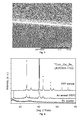
Figure 2 , the X ray diffractograms of samples prepared according to Example 2 are displayed. Selenite precipitate powder, a sample processed in air at 350 °C, and a sample subjected to rapid processing at 550 °C. - In
Figure 3 , the Raman spectrum of the sample prepared in Example 2 is displayed. - In
Figure 4 , the scanning electron micrographs of samples prepared according to Example 2 are displayed: (a) powder from precipitate in nanoparticle form; (b) a layer after processing in air at 350 °C and (c) the surface of a layer subjected to rapid thermal processing at 550 °C and (d) a cross-section of a layer subjected to rapid thermal processing at 550 °C. - In
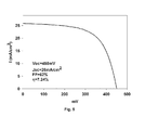
Figure 5 , a voltage-current curve of a sample prepared according Example 2 is displayed. - Below, an especially preferred embodiment of the invention is described, by way of illustration and not limitation.
- In this particular embodiment the production of Cu, In and Ga selenides is described, though the method described may be applied to other similar compounds, such as Cu, In and Ga tellurides, and others in which one or more of these elements are substituted.
- This method uses the precipitation of nanoparticles of Cu, In and Ga selenides, taking advantage of their low solubility, and describes their use in ink to deposit layers of Cu(In,Ga)Se2. Sulphates have been used as metal anions, although other soluble salts, such as nitrates, chlorides, acetates, iodides, bromides, etc. may be used:
- 1. Preparation of the chalcogenite solution (solution A). In a suitable receptacle, an equimolecular amount of hydroxide solution, preferably sodium hydroxide, and the amount of water which is enough to reach a concentration of chalcogen between 1 to 50 mM, are added to a suspension containing the acid or the oxide of the selected chalcogen element, preferably selenium.
- 2. Preparation of the solution of Cu, In and Ga salts (solution B). In order to prepare the solution of metal element salts, a mixture, preferably of Cu, In and Ga sulphates, is added to another receptacle with water, while stirring, at a molar ratio approximately equal to that of the chalcogenide to be produced. Optionally, it is possible to add to this solution some of the additional substances pointed out above. Finally, once the solution has been prepared, an equimolecular amount of hydroxide solution, preferably sodium hydroxide, and the amount of water which is enough to reach a concentration of chalcogen between 1 to 10 mM, are added.
- 3. Precipitation of the constituent elements. Once the salts have dissolved, preferably using the same reactor wherein solution B has been prepared, solution A is added dropwise until reaching a pH of 3-7. The obtained precipitate is filtered and washed with an alcoholic solvent, preferably ethanol.
- 4. Production of the ink. The obtained powder is dispersed in the alcoholic solvent and an organic reductant, preferably triethanolamine and, optionally, organic compounds having shimmering, binding, surfactant, wetting, levelling, degassing or viscosity modifying effects, are added.
- Although the best results were obtained with selenium, it has not been ruled out that it could be substituted by other elements within its group, denominated chalcogens, which are understood, for the purposes of this specification, to be the elements of group 16 of the periodic table: oxygen, sulphur, selenium, tellurium and polonium, of which, for obvious reasons, oxygen and polonium are ruled out. Thus, although within this specification reference is made to selenium in particular, what is stated also refers implicitly to sulphur and tellurium.
- A mixture of ethanol 1.4 g, triethanolamine 0.1 g and SeO2 0.6 g was placed in a glass receptacle and heated at 70 °C, stirring the mixture until dissolved. A drop of the solution was distributed with the tip of a pipette on a glass substrate coated with molybdenum, which were together placed on an electric plate at 250-300 °C for 2 minutes. The layer acquired a red colour corresponding to the formation of elemental selenium.
Figure 1 shows the cross-section of the obtained layer. - Two solutions are prepared containing:
- (A) Na2SeO3 solution, by reacting 20 mmol H2SeO3 with 40 mmol NaOH in 25 ml H2O.
- (B) Solution of the constituent metal cations: CuSO4.5H2O 0.88 g, Ga2(SO4)3.18H2O 0.3 g and In2(SO4)3.6H2O 0.615 g in 125 ml of water in a 250 ml beaker.
- Solution A was added dropwise to solution B until a pH of 3-7 was reached. The precipitate was filtered and washed with ethanol.
- The obtained powder was dispersed in ethanol and triethanolamine was added to the suspension. The composition thus obtained was deposited on a glass substrate coated with molybdenum using two 50 µm thick pieces of adhesive tape, attached in parallel on the substrate, and sliding a glass rod over them; the excess of the suspension was removed from the layer. The test piece thus obtained was placed on an electric plate at 350 °C for 2 minutes and then was subjected to rapid thermal processing using halogen radiation at a heating speed of 500 °C/min up to 550 °C.
- Characterisation of the samples: X ray diffraction analysis (
Figure 2 ) showed that the powder was initially amorphous, whereas after the first calcination at 350 °C the desired phase begins to be seen, accompanied by other binary phases. The layers subjected to rapid thermal processing at 550 °C have excellent crystallinity and, apart from peaks from the substrate, present CuIn0.7Ga0.3Se2, (JCPDS 35-1102). The efficient incorporation of the gallium was confirmed by Raman spectroscopy with the peak at 176.3 cm-1 (Figure 3 ). - The thickness of the layer, determined by scanning electron microscopy, was approximately 3 µm (
Figure 4 ). - Following the method similar to the one described in Example 2, layers of CuIn0.7Ga0.3Se2 were deposited over glass coated with molybdenum. Upon the layer thus obtained, a 50-100 nm layer of cadmium sulphide was deposited using a solution containing thiourea, NH3 and a Cd salt; on top of this, layers of ZnO and conductive ZnO doped with aluminium by means of magnetronic sputtering.
- The current-voltage characteristic of a 0.1 cm2 area was measured under simulated solar illumination. Efficiencies of 7.24 % were recorded with an open circuit voltage of 450 mV, a short circuit current of 26 mA/cm2 and fill factor of 62 % (
Figure 5 ). Furthermore, in some isolated tests, the voltage increased to 460 mV, and the efficiency to 7.5 %.
Claims (25)
- Ink composition for the in-situ production of chalcogens and/or chalcogenides characterised in that it comprises at least one chalcogenite compound having a formula selected from a group consisting of SeO2, M(SO3)n, M(SeO3)n and M(TeO3)n, wherein 0.5≤n≤2 and M is at least one metal element.
- Composition, according to claim 1, wherein said metal element M is selected from a group consisting of Cu, In and Ga.
- Composition, according to claim 1, wherein said metal element is selected from a group consisting of Sn, Zn, Cd, Sb, Ag, Au, Al, Na, K, Mg, Ca, Sr, Ba, B, V, Ti, Zr, Ge, Si, Pb, Tl, Ni, Co, Fe, Hg, V, Nb, Mn and Cr, as well as any combination thereof.
- Ink for the in-situ production of chalcogens and/or chalcogenides consisting of a suspension or solution of a composition according to any one of the claims 1 to 3.
- Method for preparing an ink for the in-situ production of chalcogens, according to claim 4, wherein said method is characterised in that it comprises mixing:(a) 1 to 20 parts by weight of at least one chalcogenite compound having a formula selected from a group consisting of SeO2, M(SO3)n, M(SeO3)n and M(TeO3)n, wherein 0.5≤n≤2 and M is at least one metal element;(b) 1 to 20 parts by weight of at least one reductant; and(c) 20 to 400 parts by weight of a solvent;
said mixture subsequently being heated while stirring at a temperature comprised between 0 °C to 100 °C until obtaining a solution constituting the ink to be prepared. - Method for preparing an ink for the in-situ production of chalcogenides, according to claim 4, wherein said method is characterised in that it comprises:(a) preparing a first solution of at least one chalcogenite compound having a formula selected from a group consisting of SeO2, M(SO3)n, M(SeO3)n and M(TeO3)n, wherein 0.5≤n≤2 and M is at least one metal element;(b) preparing a second solution of at least one salt of a second metal element and adding an equimolecular amount of a hydroxide solution and an amount of water which is enough to reach a concentration of chalcogen between 1 mM to 2 M;(c) mixing the first aqueous solution and the second aqueous solution until reaching a pH giving rise to a chalcogenite precipitate from the second metal element in the solution from step (b);(d) washing the precipitate produced in the previous step and dispersing it in a solvent; and(e) adding a reductant to the previous dispersion.
- Method, according to claim 6, wherein the salt for preparing the second aqueous solution is selected from a group consisting of sulphate, nitrate, chloride, acetate, iodide and bromide of the second metal element.
- Method, according to any one of the claims 5 to 7, wherein said reductant is an amine selected between triethanolamine and monoethanolamine.
- Method, according to any one of the claims 5 to 8, wherein said solvent is an alcoholic solvent.
- Method, according to any one of the claims 5 to 9, wherein the metal element M is selected from a group consisting of Cu, In and Ga, as well as any combination thereof.
- Method, according to any one of the claims 5 to 10, wherein the second metal element is selected from a group consisting of Sn, Zn, Cd, Sb, Ag, Au, Al, Na, K, Mg, Ca, Sr, Ba, B, V, Ti, Zr, Ge, Si, Pb, Tl, Ni, Co, Fe, Hg, V, Nb, Mn and Cr, as well as any combination thereof.
- Method, according to any one of the claims 5 to 11, wherein it comprises complementarily adding solid selenite nanoparticles with a particle size comprised between 2 to 2,000 nm.
- Method, according to any one of the claims 5 to 12, wherein it comprises complementarily adding at least one compound selected from a group consisting of organic, binding, surfactant, wetting, levelling, degassing and viscosity modifying compounds, as well as inorganic or organic solvents.
- Method, according to any one of the claims 6 to 13, wherein it comprises an additional step of preparing the chalcogenite compound by adding a suspension containing an acid or oxide of the chalcogen element, a hydroxide solution, and an amount of water which is enough to reach a concentration of chalcogen between 0.1 to 1,000 mM.
- Ink obtainable through a method according to any one of the claims 5 to 14.
- Use of an ink according to claim 4 or 15 for the in-situ preparation of a semiconductor material.
- Method for preparing a semiconductor material characterised in that it comprises depositing an ink according to claim 4 or 15 on a substrate and applying thermal processing.
- Method according to claim 17, wherein said thermal processing comprises a first thermal processing at a temperature comprised between 80 °C to 400 °C and a second thermal processing at a temperature between 80 °C to 1,200 °C.
- Method according to claim 17 or 18, wherein the thermal processing is carried out in an atmosphere containing vapours of a chalcogen element or of a compound containing a chalcogen, wherein said chalcogen is selected between Se, S and Te.
- Method, according to any one of the claims 17 to 19, wherein the deposition of the ink is carried out by printing or spraying.
- Method, according to any one of the claims 17 to 20, wherein the substrate is selected from a group consisting of glass coated with molybdenum, metal, ceramic and polymer, or any combination thereof.
- Method, according to any one of the claims 17 to 21, wherein the ink is deposited forming layers of between 1 to 100 µm thick.
- Semiconductor material obtainable through a method according to any one of the claims 17 to 22.
- Method for the manufacture of photovoltaic devices starting from a material according to claim 23, characterised in that it comprises depositing a first additional layer of at least one n-type semiconductor comprising at least one metal selected from the group Cd, Zn and In, and at least one second conductive and clear layer comprising an oxide or a mixture of oxides of at least one metal selected from the group Zn, Al, In, Sn, Sb and Cd.
- Photovoltaic device obtainable through a method according to claim 24.
Applications Claiming Priority (2)
| Application Number | Priority Date | Filing Date | Title |
|---|---|---|---|
| ES201131580A ES2402313B1 (en) | 2011-09-30 | 2011-09-30 | INKS FOR THE "IN SITU" OBTAINING OF CALCÓGENOS AND / OR CALCOGENUROS THAT GIVE PLACE TO SEMICONDUCTOR LAYERS, THEIR OBTAINING AND HOW TO USE |
| PCT/ES2012/070666 WO2013045731A1 (en) | 2011-09-30 | 2012-09-26 | Inks for the in-situ production of chalcogens and/or chalcogenides that form semiconductor layers, production method thereof and use of same |
Publications (2)
| Publication Number | Publication Date |
|---|---|
| EP2763184A1 true EP2763184A1 (en) | 2014-08-06 |
| EP2763184A4 EP2763184A4 (en) | 2015-03-04 |
Family
ID=47994328
Family Applications (1)
| Application Number | Title | Priority Date | Filing Date |
|---|---|---|---|
| EP20120836775 Withdrawn EP2763184A4 (en) | 2011-09-30 | 2012-09-26 | INKS FOR THE "IN SITU" PRODUCTION OF CHALCOGENES AND / OR CHALCOGENIDES WHICH FORM SEMICONDUCTOR LAYERS, THEIR OBTAINING AND THEIR USE |
Country Status (4)
| Country | Link |
|---|---|
| EP (1) | EP2763184A4 (en) |
| ES (1) | ES2402313B1 (en) |
| TW (1) | TW201331306A (en) |
| WO (1) | WO2013045731A1 (en) |
Family Cites Families (14)
| Publication number | Priority date | Publication date | Assignee | Title |
|---|---|---|---|---|
| US7037692B1 (en) | 1990-03-16 | 2006-05-02 | Calgene, Inc. | Plant desaturases compositions and uses |
| US6126740A (en) * | 1995-09-29 | 2000-10-03 | Midwest Research Institute | Solution synthesis of mixed-metal chalcogenide nanoparticles and spray deposition of precursor films |
| US6127202A (en) | 1998-07-02 | 2000-10-03 | International Solar Electronic Technology, Inc. | Oxide-based method of making compound semiconductor films and making related electronic devices |
| FR2849532B1 (en) | 2002-12-26 | 2005-08-19 | Electricite De France | METHOD FOR MANUFACTURING THIN FILM I-III-VI2 COMPOUND, PROMOTING THE INCORPORATION OF ELEMENTS III |
| US6875661B2 (en) | 2003-07-10 | 2005-04-05 | International Business Machines Corporation | Solution deposition of chalcogenide films |
| US8048477B2 (en) | 2004-02-19 | 2011-11-01 | Nanosolar, Inc. | Chalcogenide solar cells |
| CH697007A5 (en) | 2004-05-03 | 2008-03-14 | Solaronix Sa | Method for producing a chalcopyrite compound thin layer. |
| US8137457B2 (en) * | 2004-07-23 | 2012-03-20 | University Of Florida Research Foundation, Inc. | One-pot synthesis of high-quality metal chalcogenide nanocrystals without precursor injection |
| EP1861916A4 (en) | 2005-03-16 | 2013-03-27 | Nanosolar Inc | METALLIC DISPERSION AND FORMATION OF COMPOUND FILM FOR ACTIVE LAYER OF PHOTOVOLTAIC DEVICE |
| KR100850000B1 (en) | 2005-09-06 | 2008-08-01 | 주식회사 엘지화학 | Process for Preparation of Absorption Layer of Solar Cell |
| EP2101931B1 (en) | 2006-11-09 | 2015-05-13 | Alliance for Sustainable Energy, LLC | Precursors for formation of copper selenide, indium selenide, copper indium diselenide, and/or copper indium gallium diselenide films |
| US20090260670A1 (en) * | 2008-04-18 | 2009-10-22 | Xiao-Chang Charles Li | Precursor ink for producing IB-IIIA-VIA semiconductors |
| US8512603B2 (en) * | 2009-08-04 | 2013-08-20 | Precursor Energetics, Inc. | Polymeric precursors for CIS and CIGS photovoltaics |
| EP2504276A1 (en) * | 2009-11-25 | 2012-10-03 | E. I. du Pont de Nemours and Company | Aqueous process for producing crystalline copper chalcogenide nanoparticles, the nanoparticles so-produced, and inks and coated substrates incorporating the nanoparticles |
-
2011
- 2011-09-30 ES ES201131580A patent/ES2402313B1/en not_active Expired - Fee Related
-
2012
- 2012-09-26 EP EP20120836775 patent/EP2763184A4/en not_active Withdrawn
- 2012-09-26 WO PCT/ES2012/070666 patent/WO2013045731A1/en not_active Ceased
- 2012-09-28 TW TW101136108A patent/TW201331306A/en unknown
Also Published As
| Publication number | Publication date |
|---|---|
| ES2402313B1 (en) | 2014-03-04 |
| ES2402313A1 (en) | 2013-04-30 |
| EP2763184A4 (en) | 2015-03-04 |
| WO2013045731A1 (en) | 2013-04-04 |
| TW201331306A (en) | 2013-08-01 |
Similar Documents
| Publication | Publication Date | Title |
|---|---|---|
| US9093190B2 (en) | Synthesis of multinary chalcogenide nanoparticles comprising Cu, Zn, Sn, S, and Se | |
| US8470636B2 (en) | Aqueous process for producing crystalline copper chalcogenide nanoparticles, the nanoparticles so-produced, and inks and coated substrates incorporating the nanoparticles | |
| US20090260670A1 (en) | Precursor ink for producing IB-IIIA-VIA semiconductors | |
| Bhosale et al. | Influence of copper concentration on sprayed CZTS thin films deposited at high temperature | |
| Jin et al. | Preparation of Cu2ZnSnS4-based thin film solar cells by a combustion method | |
| JP6330051B2 (en) | Method for doping Cu (In, Ga) (S, Se) 2 nanoparticles with sodium or antimony | |
| US20130037110A1 (en) | Particle-Based Precursor Formation Method and Photovoltaic Device Thereof | |
| Kang et al. | Aqueous synthesis of wurtzite Cu2ZnSnS4 nanocrystals | |
| TWI421214B (en) | IBIIIAVIA family amorphous phase compound and method for producing IBIIIAVIA family amorphous phase precursor applied to thin film solar cell | |
| Garmim et al. | Opto-electrical properties of Ni and Mg co-doped CdS thin films prepared by spin coating technique | |
| Lv et al. | Improving the performance of low-cost water-based solution-synthesised Cu2ZnSn1-xGex (S, Se) 4 absorber thin films by germanium doping | |
| Gapanovich et al. | New absorbers for third-generation thin-film solar cells based on Cu–A–B–S–Se (A= Ba, Sr, Fe, Ni, or Mn; B= Si, Ge, or Sn) quaternary copper compounds | |
| Peng et al. | Solvothermal synthesis of Cu2Zn (Sn1− xGex) S4 and Cu2 (Sn1− xGex) S3 nanoparticles with tunable band gap energies | |
| Valls et al. | Easy and low-cost aqueous precipitation method to obtain Cu2ZnSn (S, Se) 4 thin layers | |
| JPWO2012090938A1 (en) | Compound semiconductor thin film solar cell and method for manufacturing the same | |
| Liu et al. | A non-vacuum solution route to prepare amorphous metal oxides thin films for Cu2ZnSn (S, Se) 4 solar cells | |
| Kumar et al. | The effect of the precursor molarities on the composition, microstructure and optical properties of tin sulphide films obtained from S-SILAR technique | |
| CN102815676B (en) | Polyhydric alcohol solution chemical synthesis method for preparing non-stoichiometric Cu-In-Se series compound nano-crystalline | |
| Chen et al. | Structural and optical properties of Cu2MnSnS4 thin film fabricated by sol-gel technique | |
| Xu et al. | High quality CdS buffer layer developed via Zn salt additive engineering for Sb2S3 solar cells | |
| Oliveira et al. | In-situ sol-gel synthesis and thin film deposition of Cu (In, Ga)(S, Se) 2 solar cells | |
| Fareh et al. | Influence of solution acidity on the growth, structural and optical properties of co-electrodeposited Cu2SnS3 thin films: experimental and DFT discussions | |
| ES2402313B1 (en) | INKS FOR THE "IN SITU" OBTAINING OF CALCÓGENOS AND / OR CALCOGENUROS THAT GIVE PLACE TO SEMICONDUCTOR LAYERS, THEIR OBTAINING AND HOW TO USE | |
| Mathew | Engineering the properties of indium sulfide for thin film solar cells by doping | |
| Husien | KESTERITE NANOPARTICLES FOR PHOTOVOLTAICS AND PHOTOCATALYSIS |
Legal Events
| Date | Code | Title | Description |
|---|---|---|---|
| PUAI | Public reference made under article 153(3) epc to a published international application that has entered the european phase |
Free format text: ORIGINAL CODE: 0009012 |
|
| 17P | Request for examination filed |
Effective date: 20140428 |
|
| AK | Designated contracting states |
Kind code of ref document: A1 Designated state(s): AL AT BE BG CH CY CZ DE DK EE ES FI FR GB GR HR HU IE IS IT LI LT LU LV MC MK MT NL NO PL PT RO RS SE SI SK SM TR |
|
| RIN1 | Information on inventor provided before grant (corrected) |
Inventor name: LINCOT, DANIEL Inventor name: ESCRIBANO LOPEZ, PURIFICACION Inventor name: CARDA CASTELLO, JUAN BAUTISTA Inventor name: CHASSAING, ELISABETH Inventor name: KRASSIMIROV TODOROV, TEODOR |
|
| DAX | Request for extension of the european patent (deleted) | ||
| A4 | Supplementary search report drawn up and despatched |
Effective date: 20150204 |
|
| RIC1 | Information provided on ipc code assigned before grant |
Ipc: H01L 31/0264 20060101ALI20150129BHEP Ipc: H01L 31/032 20060101ALI20150129BHEP Ipc: H01L 21/368 20060101AFI20150129BHEP |
|
| STAA | Information on the status of an ep patent application or granted ep patent |
Free format text: STATUS: THE APPLICATION IS DEEMED TO BE WITHDRAWN |
|
| 18D | Application deemed to be withdrawn |
Effective date: 20150903 |