EP2763140A2 - Compensation loop for read voltage adaptation in flash memory - Google Patents
Compensation loop for read voltage adaptation in flash memory Download PDFInfo
- Publication number
- EP2763140A2 EP2763140A2 EP14152121.1A EP14152121A EP2763140A2 EP 2763140 A2 EP2763140 A2 EP 2763140A2 EP 14152121 A EP14152121 A EP 14152121A EP 2763140 A2 EP2763140 A2 EP 2763140A2
- Authority
- EP
- European Patent Office
- Prior art keywords
- voltage
- nominal
- reads
- read
- read voltage
- Prior art date
- Legal status (The legal status is an assumption and is not a legal conclusion. Google has not performed a legal analysis and makes no representation as to the accuracy of the status listed.)
- Withdrawn
Links
- 230000006978 adaptation Effects 0.000 title claims description 23
- 238000000034 method Methods 0.000 claims abstract description 22
- 238000013507 mapping Methods 0.000 claims description 13
- 238000009826 distribution Methods 0.000 claims description 7
- 230000037361 pathway Effects 0.000 claims 1
- 238000010586 diagram Methods 0.000 description 5
- 230000014759 maintenance of location Effects 0.000 description 4
- 238000001514 detection method Methods 0.000 description 3
- 230000006870 function Effects 0.000 description 3
- 230000005540 biological transmission Effects 0.000 description 2
- 238000012360 testing method Methods 0.000 description 2
- 230000003044 adaptive effect Effects 0.000 description 1
- 238000003491 array Methods 0.000 description 1
- 238000006243 chemical reaction Methods 0.000 description 1
- 238000004891 communication Methods 0.000 description 1
- 238000012937 correction Methods 0.000 description 1
- 230000001419 dependent effect Effects 0.000 description 1
- 238000012986 modification Methods 0.000 description 1
- 230000004048 modification Effects 0.000 description 1
- 230000003287 optical effect Effects 0.000 description 1
Images


Classifications
-
- G—PHYSICS
- G11—INFORMATION STORAGE
- G11C—STATIC STORES
- G11C16/00—Erasable programmable read-only memories
- G11C16/02—Erasable programmable read-only memories electrically programmable
- G11C16/06—Auxiliary circuits, e.g. for writing into memory
- G11C16/26—Sensing or reading circuits; Data output circuits
-
- G—PHYSICS
- G11—INFORMATION STORAGE
- G11C—STATIC STORES
- G11C11/00—Digital stores characterised by the use of particular electric or magnetic storage elements; Storage elements therefor
- G11C11/56—Digital stores characterised by the use of particular electric or magnetic storage elements; Storage elements therefor using storage elements with more than two stable states represented by steps, e.g. of voltage, current, phase, frequency
- G11C11/5621—Digital stores characterised by the use of particular electric or magnetic storage elements; Storage elements therefor using storage elements with more than two stable states represented by steps, e.g. of voltage, current, phase, frequency using charge storage in a floating gate
- G11C11/5642—Sensing or reading circuits; Data output circuits
-
- G—PHYSICS
- G11—INFORMATION STORAGE
- G11C—STATIC STORES
- G11C16/00—Erasable programmable read-only memories
- G11C16/02—Erasable programmable read-only memories electrically programmable
- G11C16/06—Auxiliary circuits, e.g. for writing into memory
- G11C16/34—Determination of programming status, e.g. threshold voltage, overprogramming or underprogramming, retention
- G11C16/3418—Disturbance prevention or evaluation; Refreshing of disturbed memory data
Definitions
- the disclosure relates to the field of flash devices and to controlling voltage levels for flash devices.
- Flash devices can experience drifts or other variations in a flash cell's nominal voltage caused by retention, write endurance, or other factors. In such cases, it is not possible to detect and correct for the corresponding change in the optimal read voltage with analog voltage regulators. As such, nominal voltage offsets and random variations can degrade flash storage system performance and lifespan.
- a system for compensating nominal voltage variations of a flash device as set out in claim 1 and a method of compensating nominal voltage variations of a flash device as set out in claim 11.
- An embodiment of the disclosure includes a system for compensating for nominal voltage variation by tracking read voltage offsets.
- a flash device is configured to execute N reads. Each of the N reads is executed at a selected voltage offset from an initial nominal read voltage. This nominal voltage is tracked constantly to ensure that the resulting bit error rate is reduced at various stages of the flash device life.
- the N reads generate a respective N bit digital pattern associated with the selected voltage offsets.
- a mapping module is configured to receive the N bit digital pattern generated by the N reads. The mapping module is further configured to map the N bit digital pattern to a signed representation.
- a voltage compensator is configured to provide a voltage adjustment to the nominal read voltage based upon the statistics of observed signed representation to at least partially compensate for the deterministic and random variations of the nominal voltage.
- FIGS. 1 through 6 illustrate embodiments of a system and method for compensating nominal read voltage variations utilizing a digital adaptive compensation loop. Shifts or offsets in the nominal read voltage of a flash device result in degraded performance and shorter lifespan of disk drives and other storage systems based on flash memory components.
- a fully blind compensation scheme (requiring no pre-stored offset data) adjusts for read voltage variations across different pages, blocks, or dies.
- acquisition time can be controlled because the compensation loop is enabled to automatically acquire offsets for sets of pages or blocks without need for pre-stored values.
- a system 100 for compensating nominal read voltage variations for a flash device 102 includes at least two read paths.
- the flash device 102 is configured to execute reads utilizing a normal read path linking a decoder 104 such as, but not limited to, a soft or hard error correction coding (ECC) decoder.
- ECC soft or hard error correction coding
- the decoder 104 is a low-density parity-check (LDPC) decoder.
- the normal read path employs the nominal read voltage which is tracked using the output of the digital compensation loop.
- the compensation loop is integrated with a read-retry path of a read channel. In other embodiments, the compensation loop is in a compensation path that is distinct from or in place of the read-retry path.
- the compensation loop is accordingly enabled when a predetermined event occurs such as, but not limited to, startup, read failure, or offset detection. In some embodiments, the compensation loop is enabled periodically, manually, or at one or more selected or programmed times, such as after a selected number of program/erase memory cycles occurs (e.g. every 2000 P/E cycles).
- ADC analog-to-digital convertor
- the N bit pattern is associated with the pattern of selected voltage offsets.
- the N bit pattern includes a sequence of zeros representing the number of instances where the cell's nominal voltage is to the left of the read voltages followed by ones to complete the N bit sequence. For example, in a four read-four bit configuration, each read will result in one of the following output sequences: "0000", "0001", “0011”, “0111", and "1111".
- the simplified representation allows for rapid conversion because the nominal voltage can be compared in parallel to the read voltages.
- the sequential bit patterns simplify detection of invalid patterns (e.g. "0101 ").
- the system 100 further includes a mapping module 106 configured to receive the N bit pattern associated with the N reads.
- the mapping module 106 is further configured to map each of the N bit patterns into a signed M bit representation of a nominal voltage.
- the signed M bit binary representation is a three bit signed representation.
- the mapping module 106 is further configured to handle invalid patterns by mapping to the closest valid pattern if the corresponding Hamming distance to the closest valid pattern is smaller than a selected threshold. If the corresponding Hamming distance is not smaller than the selected threshold, the mapping module 106 may be further configured to declare the invalid pattern as erasure.
- LLR log-likelihood ratio
- the system 100 further includes an adaptation loop 108 configured to adaptively provide numerical adjustments ( ⁇ ) to the signed representation corresponding to the N reads of each cell.
- the numerical adjustments ⁇ are used by a voltage compensator 110, such as an adjustable DC source, to provide a voltage adjustment to the nominal read voltage of the normal read path and the read retry/compensation path.
- the adaptation loop 108 is configured for locking the nominal read voltage of the flash device to a value corresponding to a sufficiently reduced bit error rate.
- the voltage compensator 110 monitors the numerical adjustments over multiple cell reads in order to track the read reference voltages V A , V B , and V C .
- the read reference voltages V A , V B , and V C are optimal values or values associated with a sufficiently reduced bit error rate.
- LSB reference voltage V B compensation if ⁇ >1 then reduce the read voltage by one voltage step, and if ⁇ 0 then increase V B by one voltage offset step.
- ⁇ A controls V A and ⁇ c controls V C .
- ⁇ A could be set to equal ⁇ c in which case V A and V C are tied together.
- FIGS. 2 through 5 illustrate most significant bit (MSB) and least significant bit (LSB) zones of interest and adaptation loops 108 designed for treating MSB and LSB blocks or pages.
- MSB most significant bit
- LSB least significant bit
- FIG. 3 illustrates the adaptation loop 108 configured for LSB states.
- the system 100 is simplified by using the adaptation loop 108 illustrated in FIG. 3 to generate voltage adjustments for the LSB and MSB zones. Doing so provides a less complex system 100; however, better performance can be achieved by independently adjusting each of the LSB and MSB zones of interest with respective voltage adjustments, V A (lower MSB), V B (LSB), and V C (upper MSB).
- the adaptation loop 108 illustrated in FIG. 3 is configured to apply an initial numerical adjustment ( ⁇ old ) to the signed representation (x) associated with the N reads.
- the initial numerical adjustment ( ⁇ old ) is initiated at a default or predetermined initial value (e.g. zero).
- the initial numerical adjustment ( ⁇ old ) is initiated at one or more pre-stored values for selected blocks or sets of blocks.
- the adaptation loop 108 is further configured to determine successive numerical adjustments ( ⁇ new ) based on the adjusted value of the signed representation (y).
- FIG. 4 illustrates different zones of interest for MSB pages or blocks.
- each adaptation path has a respective numerical adjustment ( ⁇ A and ⁇ C ) and a respective adaptation step size ( ⁇ A and ⁇ B ).
- the adaptation loop 108 is further configured to bring the zero-crossing point in a distribution of LLR values to the nominal read voltage.
- the compensation loop is further configured to track offset variations per page or block over time.
- the compensation loop can be enabled during read-retry mode or at selected times (as previously discussed). In some embodiments, it is advantageous to enable the compensation loop at selected times (e.g. periodically, idle moments, startup, etc.) to control the read voltage for selected blocks or pages or to test for endurance or voltage retention.
- an LLR calculation module 112 is configured to receive the adjusted signed representation values (y) associated with the N reads.
- the LLR calculation module 112 is further configured to determine LLR values based upon the adjusted values (y).
- the constants (Kp) and (Kn) are selected based on the distribution of various states of interest. In some embodiments, for LSB blocks or pages a distinction is made between state “00" and state “01" and Kp and Kn are selected based on a respective distribution of each state. For MSB blocks or pages, a similar distinction and selection is made between states “11" and "10” (i.e. lower states) and states "00" and "10” (i.e. upper states).
- the LLR calculation module 112 employs six Kp,Kn gain values corresponding to the tails of interest for raw bit error rate (BER), namely the left and right tails between states “11" and “01” (lower MSB states), states “01” and “00” (LSB states), and states “00” and “10” (upper MSB states), respectively.
- the six Kp,Kn gains are in a reduced set to further simplify the LLR calculation.
- Kp or Kn values are determined utilizing a distribution of the adjusted (y) values.
- the distributions of one or more positive and negative values (V) are utilized to pick Kp or Kn.
- V positive and negative values
- incorporating the compensation loop into the read retry (and LLR generation) path allows for automatic offset compensation in LLR determination because the compensation loop is enabled to blindly converge to an offset that reduces raw BER.
- the compensation loop further includes or is in communication with a controller configured to keep track of read voltages for selected pages or blocks. Accordingly, the compensation loop can be used for retention testing and retention voltage shift detection.
- mapping module 106, adaptation loop 108, and LLR calculation module 112 described above include any combined or separated configuration of hardware, software, and/or firmware enabled to perform the functions or steps described herein.
- any of the foregoing components of system 100 are implemented by one or more processors configured to execute program instructions from carrier media.
- electronic circuitry is further employed.
- Many hardware, software, and firmware combinations are contemplated for implementing the foregoing components of system 100, among others. Accordingly, none of the embodiments described herein should be construed as limitations.
- FIG. 6 is a flow diagram illustrating an embodiment of a method 200 for compensating variations in nominal read voltage of a flash device 102.
- System 100 is a manifestation of method 200 and all steps or features described with regard to embodiments of system 100 or method 200 are applicable to both the system 100 and method 200. However, it is noted that one or more steps of method 200 may be executed via other means known to the art. Accordingly method 200 should be broadly construed to encompass any acceptable means for carrying out the steps described below.
- N reads are performed as part of compensation or read retry path. Each of the N reads is performed at a selected voltage offset from the initial read voltage. Step 202 is initialized at a selected time (e.g. periodically, pre-set time, manually initiated) or upon the occurrence of a specified event (e.g. read failure, corrupted read, system idle, startup).
- a specified event e.g. read failure, corrupted read, system idle, startup.
- an N bit digital pattern is generated for the N reads. The N bit digital pattern is associated with the respective voltage offsets of the N reads.
- the N bit digital pattern is mapped to an M bit signed representation of the nominal read voltage (i.e. a selected or pre-determined voltage).
- a voltage adjustment is applied based on the signed representation.
- a compensation loop adaptively generates a voltage adjustment offset to adjust the nominal read voltage up or down.
- the compensation loop adaptively provides new voltage adjustments for a selected number of cycles or until a threshold voltage is achieved. Accordingly, the nominal read voltage variations are digitally compensated without prior knowledge of optimal or ideal offset values.
- a computing system may include, but is not limited to, a personal computing system, mainframe computing system, workstation, image computer, parallel processor, or any other device known in the art.
- computing system is broadly defined to encompass any device having one or more processors, which execute instructions from a memory medium.
- the carrier medium may be a transmission medium, such as, but not limited to, a wire, cable, or wireless transmission link.
- the carrier medium may also include a storage medium such as, but not limited to, a read-only memory, a random access memory, a magnetic or optical disk, or a magnetic tape.
- Embodiments manifesting methods described herein may include storing results in a storage medium. After the results have been stored, the results can be accessed in the storage medium and used by any of the method or system embodiments described herein, formatted for display to a user, used by another software module, method, or system, etc. Furthermore, the results may be stored "permanently,” “semi-permanently,” temporarily, or for some period of time.
- the storage medium may be random access memory (RAM), and the results may not necessarily persist indefinitely in the storage medium.
- any embodiment of the disclosure manifested above as a system or method may include at least a portion of any other embodiment described herein.
- Those having skill in the art will appreciate that there are various embodiments by which systems and methods described herein can be effected, and that the implementation will vary with the context in which an embodiment of the disclosure deployed.
Landscapes
- Engineering & Computer Science (AREA)
- Computer Hardware Design (AREA)
- Techniques For Improving Reliability Of Storages (AREA)
- Read Only Memory (AREA)
Abstract
The disclosure is directed to a system and method for compensating nominal read voltage variations of a flash device. N reads are performed, each at a selected voltage offset from an initial read voltage. An N bit digital pattern associated with the selected voltage offsets is generated for the N reads. The N bit digital pattern generated by the N reads is mapped to a signed representation. A voltage adjustment based upon the signed representation is applied to at least partially compensate for a variation of the nominal read voltage to reduce bit error rate of the flash device.

Description
- The disclosure relates to the field of flash devices and to controlling voltage levels for flash devices.
- Flash devices can experience drifts or other variations in a flash cell's nominal voltage caused by retention, write endurance, or other factors. In such cases, it is not possible to detect and correct for the corresponding change in the optimal read voltage with analog voltage regulators. As such, nominal voltage offsets and random variations can degrade flash storage system performance and lifespan.
- According to a first aspect of the present invention there is provided a system for compensating nominal voltage variations of a flash device as set out in
claim 1, and a method of compensating nominal voltage variations of a flash device as set out in claim 11. - An embodiment of the disclosure includes a system for compensating for nominal voltage variation by tracking read voltage offsets. At a selected time or upon the occurrence of a predetermined event, a flash device is configured to execute N reads. Each of the N reads is executed at a selected voltage offset from an initial nominal read voltage. This nominal voltage is tracked constantly to ensure that the resulting bit error rate is reduced at various stages of the flash device life. The N reads generate a respective N bit digital pattern associated with the selected voltage offsets. A mapping module is configured to receive the N bit digital pattern generated by the N reads. The mapping module is further configured to map the N bit digital pattern to a signed representation. A voltage compensator is configured to provide a voltage adjustment to the nominal read voltage based upon the statistics of observed signed representation to at least partially compensate for the deterministic and random variations of the nominal voltage.
- Other alternative or preferred features of embodiments may be as set out in the dependent claims.
- It is to be understood that both the foregoing general description and the following detailed description are not necessarily restrictive of the disclosure. The accompanying drawings, which are incorporated in and constitute a part of the specification, illustrate embodiments of the disclosure.
- The embodiments of the disclosure may be better understood by those skilled in the art by reference to the accompanying figures in which:
- FIG. 1
- is a block diagram illustrating a system for compensating a nominal read voltage variation, in accordance with an embodiment of the disclosure;
- FIG. 2
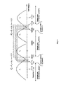
- includes a first graph illustrating a least significant bit (LSB) zone of interest and a second graph illustrating two most significant bit (MSB) zones of interest, in accordance with an embodiment of the disclosure;
- FIG. 3
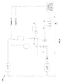
- is a block diagram illustrating an adaptation loop of the system, in accordance with an embodiment of the disclosure;
- FIG. 4
- includes a graph illustrating the two most significant bit (MSB) zones of interest, wherein digital patterns are assigned to a first MSB zone of interest and a second MSB zone of interest, in accordance with an embodiment of the disclosure;
- FIG. 5
- is a block diagram illustrating an adaptation loop of the system configured to apply a first adaptation path for nominal voltages falling in the first MSB zone of interest and a second adaptation path for nominal voltages falling in the second MSB zone of interest, in accordance with an embodiment of the disclosure; and
- FIG. 6
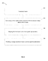
- is a flow diagram illustrating a method of compensating a nominal read voltage variation, in accordance with an embodiment of the disclosure.
- Reference will now be made in detail to the embodiments disclosed, which are illustrated in the accompanying drawings.
-
FIGS. 1 through 6 illustrate embodiments of a system and method for compensating nominal read voltage variations utilizing a digital adaptive compensation loop. Shifts or offsets in the nominal read voltage of a flash device result in degraded performance and shorter lifespan of disk drives and other storage systems based on flash memory components. In some embodiments, a fully blind compensation scheme (requiring no pre-stored offset data) adjusts for read voltage variations across different pages, blocks, or dies. Furthermore, acquisition time can be controlled because the compensation loop is enabled to automatically acquire offsets for sets of pages or blocks without need for pre-stored values. - In an embodiment, as illustrated in
FIG. 1 , asystem 100 for compensating nominal read voltage variations for aflash device 102 includes at least two read paths. When the compensation loop is not enabled, theflash device 102 is configured to execute reads utilizing a normal read path linking adecoder 104 such as, but not limited to, a soft or hard error correction coding (ECC) decoder. In some embodiments, thedecoder 104 is a low-density parity-check (LDPC) decoder. The normal read path employs the nominal read voltage which is tracked using the output of the digital compensation loop. - In some embodiments, the compensation loop is integrated with a read-retry path of a read channel. In other embodiments, the compensation loop is in a compensation path that is distinct from or in place of the read-retry path. The compensation loop is accordingly enabled when a predetermined event occurs such as, but not limited to, startup, read failure, or offset detection. In some embodiments, the compensation loop is enabled periodically, manually, or at one or more selected or programmed times, such as after a selected number of program/erase memory cycles occurs (e.g. every 2000 P/E cycles).
- When the compensation loop is enabled, the
flash device 102 is configured to perform a selected number of reads, N reads. Each of the N reads is performed at a respective voltage offset from an initial nominal read voltage of theflash device 102. Theflash device 102 is further configured to output a digital pattern for the N reads having a selected number of bits. In some embodiments, the number of reads is equivalent to the number of bits in the output digital pattern (i.e. N reads = N bit pattern). In some embodiments, theflash device 102 further includes an analog-to-digital convertor (ADC), such as a flash ADC, configured to provide the N bit pattern for the N read retries. - The N bit pattern is associated with the pattern of selected voltage offsets. In some embodiments, the N bit pattern includes a sequence of zeros representing the number of instances where the cell's nominal voltage is to the left of the read voltages followed by ones to complete the N bit sequence. For example, in a four read-four bit configuration, each read will result in one of the following output sequences: "0000", "0001", "0011", "0111", and "1111". The simplified representation allows for rapid conversion because the nominal voltage can be compared in parallel to the read voltages. Furthermore, the sequential bit patterns simplify detection of invalid patterns (e.g. "0101 ").
- The
system 100 further includes amapping module 106 configured to receive the N bit pattern associated with the N reads. Themapping module 106 is further configured to map each of the N bit patterns into a signed M bit representation of a nominal voltage. In some embodiments, the signed M bit binary representation is a three bit signed representation. In some embodiments, themapping module 106 is further configured to handle invalid patterns by mapping to the closest valid pattern if the corresponding Hamming distance to the closest valid pattern is smaller than a selected threshold. If the corresponding Hamming distance is not smaller than the selected threshold, themapping module 106 may be further configured to declare the invalid pattern as erasure. In some embodiments, themapping module 106 is further configured to set a respective log-likelihood ratio (LLR) of an erasure pattern to a selected value (e.g. LLR = 0). - The
system 100 further includes anadaptation loop 108 configured to adaptively provide numerical adjustments (λ) to the signed representation corresponding to the N reads of each cell. The numerical adjustments λ are used by avoltage compensator 110, such as an adjustable DC source, to provide a voltage adjustment to the nominal read voltage of the normal read path and the read retry/compensation path. In some embodiments, theadaptation loop 108 is configured for locking the nominal read voltage of the flash device to a value corresponding to a sufficiently reduced bit error rate. - The
voltage compensator 110 monitors the numerical adjustments over multiple cell reads in order to track the read reference voltages VA, VB, and VC. In some embodiments, the read reference voltages VA, VB, and VC are optimal values or values associated with a sufficiently reduced bit error rate. For LSB reference voltage VB compensation, if λ>1 then reduce the read voltage by one voltage step, and if λ<0 then increase VB by one voltage offset step. For MSB reference voltage compensations, λA controls VA and λc controls VC. In practice, λA could be set to equal λc in which case VA and VC are tied together. -
FIGS. 2 through 5 illustrate most significant bit (MSB) and least significant bit (LSB) zones of interest andadaptation loops 108 designed for treating MSB and LSB blocks or pages. As shown inFIG. 2 , there is generally one LSB zone of interest located between state "00" and state "01" and two MSB zones of interest, one located between "11" and "10" (i.e. lower states) and another located between states "00" and "10" (i.e. upper states).FIG. 3 illustrates theadaptation loop 108 configured for LSB states. In some embodiments, thesystem 100 is simplified by using theadaptation loop 108 illustrated inFIG. 3 to generate voltage adjustments for the LSB and MSB zones. Doing so provides a lesscomplex system 100; however, better performance can be achieved by independently adjusting each of the LSB and MSB zones of interest with respective voltage adjustments, VA (lower MSB), VB (LSB), and VC (upper MSB). - The
adaptation loop 108 illustrated inFIG. 3 is configured to apply an initial numerical adjustment (λold) to the signed representation (x) associated with the N reads. In some embodiments, the initial numerical adjustment (λold) is initiated at a default or predetermined initial value (e.g. zero). In some embodiments, the initial numerical adjustment (λold) is initiated at one or more pre-stored values for selected blocks or sets of blocks. Theadaptation loop 108 is further configured to determine successive numerical adjustments (λnew) based on the adjusted value of the signed representation (y). In some embodiments, the numerical adjustment (λ) is determined in accordance with the following equation: λnew = λold + µ*sgn(y), where µ is the adaptation step size, and λnew is adjusted only if |y| ≤ T, where T is a selected threshold. -
FIG. 4 illustrates different zones of interest for MSB pages or blocks. A first zone (R_select = 0) is associated with the lower MSB states "11" and "10" and a second zone (R_select = 1) is associated with the upper MSB states "00" and "10". All other regions (R_select = 2) are reliable or belong to LSB pages or blocks, accordingly voltages falling in R_select = 2 regions for MSB pages or blocks can be ignored. In some embodiments, as illustrated inFIG. 5 , theadaptation loop 108 is designed to handle R_select = 1 inputs and R_select = 2 with different adaptation paths. In some embodiments, each adaptation path has a respective numerical adjustment (λA and λC) and a respective adaptation step size (µA and µB). By allowing different adaptation loops for the LSB zone of interest each of the MSB zones of interest it is possible to achieve better reduction in bit error rate because the nominal read voltage adjustments (VA, VB, and VC) are tailored to each zone of interest. - In some embodiments, the
adaptation loop 108 is further configured to bring the zero-crossing point in a distribution of LLR values to the nominal read voltage. In some embodiments, the compensation loop is further configured to track offset variations per page or block over time. The compensation loop can be enabled during read-retry mode or at selected times (as previously discussed). In some embodiments, it is advantageous to enable the compensation loop at selected times (e.g. periodically, idle moments, startup, etc.) to control the read voltage for selected blocks or pages or to test for endurance or voltage retention. - In some embodiments, where the compensation loop is integrated with the read retry path of a read channel (see
FIG. 1 ), anLLR calculation module 112 is configured to receive the adjusted signed representation values (y) associated with the N reads. TheLLR calculation module 112 is further configured to determine LLR values based upon the adjusted values (y). In some embodiments, LLR values are determined for the N reads in accordance with the following equation: LLR = K(y)*y, where K(y) is a constant based upon the adjusted values (y). In some embodiments, K(y) is characterized by at least two constants including a first constant (Kp) and a second constant (Kn), such that K(y) = Kp when y ≥ 0, and K(y) = Kn when y ≤ 0. The constants (Kp) and (Kn) are selected based on the distribution of various states of interest. In some embodiments, for LSB blocks or pages a distinction is made between state "00" and state "01" and Kp and Kn are selected based on a respective distribution of each state. For MSB blocks or pages, a similar distinction and selection is made between states "11" and "10" (i.e. lower states) and states "00" and "10" (i.e. upper states). Accordingly, theLLR calculation module 112 employs six Kp,Kn gain values corresponding to the tails of interest for raw bit error rate (BER), namely the left and right tails between states "11" and "01" (lower MSB states), states "01" and "00" (LSB states), and states "00" and "10" (upper MSB states), respectively. In some embodiments, the six Kp,Kn gains are in a reduced set to further simplify the LLR calculation. - In some embodiments, Kp or Kn values are determined utilizing a distribution of the adjusted (y) values. The distributions of one or more positive and negative values (V) are utilized to pick Kp or Kn. Consider an embodiment where V=2. The number N(2) of hits where y==+2 and y==-2 are counted within a selected time window and compared against a selected count threshold (Th). Then if N(2) > Th, Kp = 1, otherwise Kp = 2. Similarly, if N(-2) > Th, Kn = 1, otherwise Kn = 2. The foregoing embodiment is illustrative of the concept for selecting Kp and Kn constants. Accordingly, the values used are intended as examples and not limitations of the disclosure.
- In some embodiments, incorporating the compensation loop into the read retry (and LLR generation) path allows for automatic offset compensation in LLR determination because the compensation loop is enabled to blindly converge to an offset that reduces raw BER. In some embodiments, the compensation loop further includes or is in communication with a controller configured to keep track of read voltages for selected pages or blocks. Accordingly, the compensation loop can be used for retention testing and retention voltage shift detection.
- The
mapping module 106,adaptation loop 108, andLLR calculation module 112 described above include any combined or separated configuration of hardware, software, and/or firmware enabled to perform the functions or steps described herein. In some embodiments, any of the foregoing components ofsystem 100 are implemented by one or more processors configured to execute program instructions from carrier media. In some embodiments, electronic circuitry is further employed. Many hardware, software, and firmware combinations are contemplated for implementing the foregoing components ofsystem 100, among others. Accordingly, none of the embodiments described herein should be construed as limitations. -
FIG. 6 is a flow diagram illustrating an embodiment of amethod 200 for compensating variations in nominal read voltage of aflash device 102.System 100 is a manifestation ofmethod 200 and all steps or features described with regard to embodiments ofsystem 100 ormethod 200 are applicable to both thesystem 100 andmethod 200. However, it is noted that one or more steps ofmethod 200 may be executed via other means known to the art. Accordinglymethod 200 should be broadly construed to encompass any acceptable means for carrying out the steps described below. - At
step 202, N reads are performed as part of compensation or read retry path. Each of the N reads is performed at a selected voltage offset from the initial read voltage. Step 202 is initialized at a selected time (e.g. periodically, pre-set time, manually initiated) or upon the occurrence of a specified event (e.g. read failure, corrupted read, system idle, startup). Atstep 204, an N bit digital pattern is generated for the N reads. The N bit digital pattern is associated with the respective voltage offsets of the N reads. Atstep 206, the N bit digital pattern is mapped to an M bit signed representation of the nominal read voltage (i.e. a selected or pre-determined voltage). Atstep 208, a voltage adjustment is applied based on the signed representation. In some embodiments, a compensation loop adaptively generates a voltage adjustment offset to adjust the nominal read voltage up or down. The compensation loop adaptively provides new voltage adjustments for a selected number of cycles or until a threshold voltage is achieved. Accordingly, the nominal read voltage variations are digitally compensated without prior knowledge of optimal or ideal offset values. - It should be recognized that in some embodiments the various functions or steps described throughout the present disclosure may be carried out by any combination of hardware, software, or firmware. In some embodiments, various steps or functions are carried out by one or more of the following: electronic circuits, logic gates, field programmable gate arrays, multiplexers, or computing systems. A computing system may include, but is not limited to, a personal computing system, mainframe computing system, workstation, image computer, parallel processor, or any other device known in the art. In general, the term "computing system" is broadly defined to encompass any device having one or more processors, which execute instructions from a memory medium.
- Program instructions implementing methods, such as those manifested by embodiments described herein, may be transmitted over or stored on carrier medium. The carrier medium may be a transmission medium, such as, but not limited to, a wire, cable, or wireless transmission link. The carrier medium may also include a storage medium such as, but not limited to, a read-only memory, a random access memory, a magnetic or optical disk, or a magnetic tape.
- Embodiments manifesting methods described herein may include storing results in a storage medium. After the results have been stored, the results can be accessed in the storage medium and used by any of the method or system embodiments described herein, formatted for display to a user, used by another software module, method, or system, etc. Furthermore, the results may be stored "permanently," "semi-permanently," temporarily, or for some period of time. For example, the storage medium may be random access memory (RAM), and the results may not necessarily persist indefinitely in the storage medium.
- It is further contemplated that any embodiment of the disclosure manifested above as a system or method may include at least a portion of any other embodiment described herein. Those having skill in the art will appreciate that there are various embodiments by which systems and methods described herein can be effected, and that the implementation will vary with the context in which an embodiment of the disclosure deployed.
- Furthermore, it is to be understood that the invention is defined by the appended claims. Although embodiments of this invention have been illustrated, it is apparent that various modifications may be made by those skilled in the art without departing from the scope and spirit of the disclosure.
Claims (16)
- A system for compensating nominal voltage variations of a flash device, comprising:a flash device configured to execute N reads, each of the N reads having a selected voltage offset from an initial nominal read voltage, the N reads generating an N bit digital pattern associated with the selected voltage offsets;a mapping module configured to receive the N bit digital pattern generated by the N reads, the mapping module further configured to map the N bit digital pattern to a signed representation; anda voltage compensator configured to provide a voltage adjustment based upon the signed representation to at least partially compensate for a variation of the nominal read voltage.
- The system of claim 1, wherein the flash device includes a flash analog-to-digital converter configured to generate the N bit digital pattern associated with the N reads.
- The system of claim 1, wherein the system is configured to compensate for nominal voltage variations after a selected number of memory cycles occur or after a read failure occurs.
- The system of claim 1, further comprising:an adaptation loop configured to receive the signed representation from the mapping module, the adaptation loop further configured to adaptively provide one or more numerical adjustments based upon the magnitude and sign of the signed representation, wherein the voltage adjustment is determined utilizing the one or more numerical adjustments from the adaptation loop.
- The system of claim1, further comprising
a calculation module configured to determine a log-likelihood ratio based upon an adjusted nominal read voltage. - The system of claim 5, wherein the log-likelihood ratio (LLR) is determined in accordance with the following equation:

where y is the adjusted read voltage, and K(y) is a constant based upon y. - The system of claim 6, whereinK(y) = Kp when y is not less than zero, andK(y) = Kn when y is less than zero,where Kp and Kn are selected constants.
- The system of claim 7, wherein Kp and Kn are determined utilizing a distribution of values for y.
- The system of claim 1, wherein the system is configured to compensate for nominal voltage variations after a read failure occurs, wherein the system includes at least a portion of a read-retry pathway.
- The system of claim 1, wherein the signed representation includes a three bit signed binary representation.
- A method of compensating nominal voltage variations of a flash device, comprising:executing N reads, each of the N reads having a selected voltage offset from an initial nominal read voltage;generating an N bit digital pattern associated with the selected voltage offsets;mapping the N bit digital pattern to a signed representation; andproviding a voltage adjustment based upon the signed representation to at least partially compensate for a variation of the nominal read voltage.
- The method of claim 11, further comprising:adaptively providing one or more numerical adjustments based upon the magnitude and sign of the signed representation, wherein the voltage adjustment is determined utilizing the one or more numerical adjustments.
- The method of claim 11, further comprising:determining a log-likelihood ratio based upon an adjusted nominal read voltage.
- The method of claim 13, wherein the log-likelihood ratio (LLR) is determined in accordance with the following equation:

where y is the adjusted read voltage, and K(y) is a constant based upon y. - The method of claim 14, whereinK(y) = Kp when y is not less than zero, andK(y) = Kn when y is less than zero,where Kp and Kn are selected constants.
- The method of claim 15, wherein Kp and Kn are determined utilizing a distribution of values for y.
Applications Claiming Priority (1)
| Application Number | Priority Date | Filing Date | Title |
|---|---|---|---|
| US13/757,027 US8879324B2 (en) | 2013-02-01 | 2013-02-01 | Compensation loop for read voltage adaptation |
Publications (1)
| Publication Number | Publication Date |
|---|---|
| EP2763140A2 true EP2763140A2 (en) | 2014-08-06 |
Family
ID=49999755
Family Applications (1)
| Application Number | Title | Priority Date | Filing Date |
|---|---|---|---|
| EP14152121.1A Withdrawn EP2763140A2 (en) | 2013-02-01 | 2014-01-22 | Compensation loop for read voltage adaptation in flash memory |
Country Status (6)
| Country | Link |
|---|---|
| US (1) | US8879324B2 (en) |
| EP (1) | EP2763140A2 (en) |
| JP (1) | JP6556423B2 (en) |
| KR (1) | KR102180452B1 (en) |
| CN (1) | CN103971723B (en) |
| TW (1) | TWI613661B (en) |
Families Citing this family (16)
| Publication number | Priority date | Publication date | Assignee | Title |
|---|---|---|---|---|
| US9286155B1 (en) * | 2013-05-24 | 2016-03-15 | Marvell International Ltd. | Systems and methods for generating soft information in a flash device |
| US9818488B2 (en) * | 2015-10-30 | 2017-11-14 | Seagate Technology Llc | Read threshold voltage adaptation using bit error rates based on decoded data |
| US9633740B1 (en) * | 2016-02-11 | 2017-04-25 | Seagate Technology Llc | Read retry operations where likelihood value assignments change sign at different read voltages for each read retry |
| US9905302B2 (en) | 2014-11-20 | 2018-02-27 | Western Digital Technologies, Inc. | Read level grouping algorithms for increased flash performance |
| US9576671B2 (en) | 2014-11-20 | 2017-02-21 | Western Digital Technologies, Inc. | Calibrating optimal read levels |
| US9720754B2 (en) | 2014-11-20 | 2017-08-01 | Western Digital Technologies, Inc. | Read level grouping for increased flash performance |
| KR102253592B1 (en) * | 2014-12-23 | 2021-05-18 | 삼성전자주식회사 | Data storage device for compensating initial threshold voltage distribution shift, method thereof, and data processing system including the same |
| GB2537484B (en) * | 2015-03-20 | 2019-07-03 | HGST Netherlands BV | Read level grouping for increased flash performance |
| US10324648B1 (en) | 2016-04-28 | 2019-06-18 | Seagate Technology Llc | Wear-based access optimization |
| US9971646B2 (en) | 2016-06-01 | 2018-05-15 | Apple Inc. | Reading-threshold setting based on data encoded with a multi-component code |
| US10120585B2 (en) * | 2016-08-10 | 2018-11-06 | SK Hynix Inc. | Memory system of optimal read reference voltage and operating method thereof |
| JP6659494B2 (en) * | 2016-08-19 | 2020-03-04 | キオクシア株式会社 | Semiconductor storage device and memory system |
| US9953709B2 (en) | 2016-09-06 | 2018-04-24 | Toshiba Memory Corporation | Semiconductor memory device and memory system |
| KR20180051272A (en) * | 2016-11-08 | 2018-05-16 | 에스케이하이닉스 주식회사 | Data storage device and operating method thereof |
| CN110299177B (en) * | 2019-07-04 | 2021-01-19 | 合肥联诺科技有限公司 | Charge compensation circuit for reducing read operation voltage jitter and memory structure |
| US11587627B2 (en) | 2021-04-16 | 2023-02-21 | Micron Technology, Inc. | Determining voltage offsets for memory read operations |
Family Cites Families (14)
| Publication number | Priority date | Publication date | Assignee | Title |
|---|---|---|---|---|
| KR100408688B1 (en) * | 2001-10-23 | 2003-12-06 | 주식회사 하이닉스반도체 | A circuit for compensating offset voltage of an operational amplifier |
| US6956770B2 (en) * | 2003-09-17 | 2005-10-18 | Sandisk Corporation | Non-volatile memory and method with bit line compensation dependent on neighboring operating modes |
| EP2067143B1 (en) * | 2006-09-27 | 2014-01-08 | SanDisk Technologies Inc. | Memory with cell population distribution assisted read margining |
| KR100888842B1 (en) * | 2007-06-28 | 2009-03-17 | 삼성전자주식회사 | Flash memory device that can optimize the read voltage and how to set its read voltage |
| US8117375B2 (en) * | 2007-10-17 | 2012-02-14 | Micron Technology, Inc. | Memory device program window adjustment |
| JP2012504820A (en) * | 2008-09-30 | 2012-02-23 | エルエスアイ コーポレーション | Method and apparatus for soft data generation of memory device based on performance factor adjustment |
| JP4818381B2 (en) * | 2009-03-02 | 2011-11-16 | 株式会社東芝 | Semiconductor memory device |
| KR101027501B1 (en) * | 2009-07-10 | 2011-04-06 | 쓰리에이로직스(주) | RF reader, its offset voltage compensation method and RF system including the same |
| US20110041005A1 (en) * | 2009-08-11 | 2011-02-17 | Selinger Robert D | Controller and Method for Providing Read Status and Spare Block Management Information in a Flash Memory System |
| US8077515B2 (en) * | 2009-08-25 | 2011-12-13 | Micron Technology, Inc. | Methods, devices, and systems for dealing with threshold voltage change in memory devices |
| KR101618311B1 (en) * | 2010-02-08 | 2016-05-04 | 삼성전자주식회사 | Flash memory device and reading method thereof |
| US20120008414A1 (en) * | 2010-07-06 | 2012-01-12 | Michael Katz | Systems and methods for storing, retrieving, and adjusting read thresholds in flash memory storage system |
| US8737136B2 (en) * | 2010-07-09 | 2014-05-27 | Stec, Inc. | Apparatus and method for determining a read level of a memory cell based on cycle information |
| KR101868332B1 (en) * | 2010-11-25 | 2018-06-20 | 삼성전자주식회사 | Flash memory device and data storage device including the same |
-
2013
- 2013-02-01 US US13/757,027 patent/US8879324B2/en not_active Expired - Fee Related
-
2014
- 2014-01-10 TW TW103100934A patent/TWI613661B/en not_active IP Right Cessation
- 2014-01-20 CN CN201410025203.6A patent/CN103971723B/en not_active Expired - Fee Related
- 2014-01-22 EP EP14152121.1A patent/EP2763140A2/en not_active Withdrawn
- 2014-01-27 JP JP2014012282A patent/JP6556423B2/en not_active Expired - Fee Related
- 2014-01-28 KR KR1020140010149A patent/KR102180452B1/en not_active Expired - Fee Related
Non-Patent Citations (1)
| Title |
|---|
| None |
Also Published As
| Publication number | Publication date |
|---|---|
| JP2014149906A (en) | 2014-08-21 |
| JP6556423B2 (en) | 2019-08-07 |
| CN103971723A (en) | 2014-08-06 |
| TW201440060A (en) | 2014-10-16 |
| US20140219028A1 (en) | 2014-08-07 |
| KR102180452B1 (en) | 2020-11-18 |
| KR20140099196A (en) | 2014-08-11 |
| CN103971723B (en) | 2017-07-11 |
| TWI613661B (en) | 2018-02-01 |
| US8879324B2 (en) | 2014-11-04 |
Similar Documents
| Publication | Publication Date | Title |
|---|---|---|
| US8879324B2 (en) | Compensation loop for read voltage adaptation | |
| US10276233B1 (en) | Adaptive read threshold voltage tracking with charge leakage mitigation using threshold voltage offsets | |
| US10180868B2 (en) | Adaptive read threshold voltage tracking with bit error rate estimation based on non-linear syndrome weight mapping | |
| US9633740B1 (en) | Read retry operations where likelihood value assignments change sign at different read voltages for each read retry | |
| US20190130967A1 (en) | Adaptive read threshold voltage tracking with charge leakage mitigation using charge leakage settling time | |
| US9367389B2 (en) | Recovery strategy that reduces errors misidentified as reliable | |
| US9209835B2 (en) | Read retry for non-volatile memories | |
| US8760932B2 (en) | Determination of memory read reference and programming voltages | |
| US7568135B2 (en) | Use of alternative value in cell detection | |
| EP2221823B1 (en) | Maintenance operations for multi-level data storage cells | |
| KR101403429B1 (en) | Apparatus and method of multi-bit programming | |
| US7649793B1 (en) | Channel estimation for multi-level memories using pilot signals | |
| US10176041B2 (en) | Deterministic read retry method for soft LDPC decoding in flash memories | |
| US20180012663A1 (en) | Independent read threshold voltage tracking for multiple dependent read threshold voltages using syndrome weights | |
| US8484519B2 (en) | Optimal programming levels for LDPC | |
| US20120239991A1 (en) | Apparatus and method for determining an operating condition of a memory cell based on cycle information | |
| US20160027521A1 (en) | Method of flash channel calibration with multiple luts for adaptive multiple-read | |
| JP5457339B2 (en) | Memory cell read level control apparatus and method | |
| US9582359B2 (en) | Write mapping to mitigate hard errors via soft-decision decoding | |
| US20070263441A1 (en) | Analog Interface for a Flash Memory Die | |
| US20140325314A1 (en) | Read bias management to reduce read errors for phase change memory | |
| WO2007134244A2 (en) | Use of 8-bit or higher a/d for nand cell value | |
| KR20170054277A (en) | Adaptive read threshold voltage tracking with separate characterization on each side of voltage distribution about distribution mean | |
| US20220197742A1 (en) | Customized parameterization of read parameters after a decoding failure for solid state storage devices | |
| US20120110401A1 (en) | System and method of sensing data in a semiconductor device |
Legal Events
| Date | Code | Title | Description |
|---|---|---|---|
| PUAI | Public reference made under article 153(3) epc to a published international application that has entered the european phase |
Free format text: ORIGINAL CODE: 0009012 |
|
| 17P | Request for examination filed |
Effective date: 20140122 |
|
| AK | Designated contracting states |
Kind code of ref document: A2 Designated state(s): AL AT BE BG CH CY CZ DE DK EE ES FI FR GB GR HR HU IE IS IT LI LT LU LV MC MK MT NL NO PL PT RO RS SE SI SK SM TR |
|
| AX | Request for extension of the european patent |
Extension state: BA ME |
|
| STAA | Information on the status of an ep patent application or granted ep patent |
Free format text: STATUS: THE APPLICATION IS DEEMED TO BE WITHDRAWN |
|
| 18D | Application deemed to be withdrawn |
Effective date: 20160802 |