EP2762913A1 - Highly integrated circuit architecture - Google Patents
Highly integrated circuit architecture Download PDFInfo
- Publication number
- EP2762913A1 EP2762913A1 EP14163942.7A EP14163942A EP2762913A1 EP 2762913 A1 EP2762913 A1 EP 2762913A1 EP 14163942 A EP14163942 A EP 14163942A EP 2762913 A1 EP2762913 A1 EP 2762913A1
- Authority
- EP
- European Patent Office
- Prior art keywords
- vco
- signal
- receive
- tuning
- transmit
- Prior art date
- Legal status (The legal status is an assumption and is not a legal conclusion. Google has not performed a legal analysis and makes no representation as to the accuracy of the status listed.)
- Granted
Links
Images



Classifications
-
- G—PHYSICS
- G01—MEASURING; TESTING
- G01S—RADIO DIRECTION-FINDING; RADIO NAVIGATION; DETERMINING DISTANCE OR VELOCITY BY USE OF RADIO WAVES; LOCATING OR PRESENCE-DETECTING BY USE OF THE REFLECTION OR RERADIATION OF RADIO WAVES; ANALOGOUS ARRANGEMENTS USING OTHER WAVES
- G01S7/00—Details of systems according to groups G01S13/00, G01S15/00, G01S17/00
- G01S7/02—Details of systems according to groups G01S13/00, G01S15/00, G01S17/00 of systems according to group G01S13/00
- G01S7/03—Details of HF subsystems specially adapted therefor, e.g. common to transmitter and receiver
- G01S7/032—Constructional details for solid-state radar subsystems
-
- G—PHYSICS
- G01—MEASURING; TESTING
- G01S—RADIO DIRECTION-FINDING; RADIO NAVIGATION; DETERMINING DISTANCE OR VELOCITY BY USE OF RADIO WAVES; LOCATING OR PRESENCE-DETECTING BY USE OF THE REFLECTION OR RERADIATION OF RADIO WAVES; ANALOGOUS ARRANGEMENTS USING OTHER WAVES
- G01S7/00—Details of systems according to groups G01S13/00, G01S15/00, G01S17/00
- G01S7/02—Details of systems according to groups G01S13/00, G01S15/00, G01S17/00 of systems according to group G01S13/00
- G01S7/35—Details of non-pulse systems
-
- G—PHYSICS
- G01—MEASURING; TESTING
- G01S—RADIO DIRECTION-FINDING; RADIO NAVIGATION; DETERMINING DISTANCE OR VELOCITY BY USE OF RADIO WAVES; LOCATING OR PRESENCE-DETECTING BY USE OF THE REFLECTION OR RERADIATION OF RADIO WAVES; ANALOGOUS ARRANGEMENTS USING OTHER WAVES
- G01S7/00—Details of systems according to groups G01S13/00, G01S15/00, G01S17/00
- G01S7/02—Details of systems according to groups G01S13/00, G01S15/00, G01S17/00 of systems according to group G01S13/00
- G01S7/40—Means for monitoring or calibrating
- G01S7/4004—Means for monitoring or calibrating of parts of a radar system
- G01S7/4008—Means for monitoring or calibrating of parts of a radar system of transmitters
-
- G—PHYSICS
- G01—MEASURING; TESTING
- G01S—RADIO DIRECTION-FINDING; RADIO NAVIGATION; DETERMINING DISTANCE OR VELOCITY BY USE OF RADIO WAVES; LOCATING OR PRESENCE-DETECTING BY USE OF THE REFLECTION OR RERADIATION OF RADIO WAVES; ANALOGOUS ARRANGEMENTS USING OTHER WAVES
- G01S13/00—Systems using the reflection or reradiation of radio waves, e.g. radar systems; Analogous systems using reflection or reradiation of waves whose nature or wavelength is irrelevant or unspecified
- G01S13/88—Radar or analogous systems specially adapted for specific applications
- G01S13/93—Radar or analogous systems specially adapted for specific applications for anti-collision purposes
- G01S13/931—Radar or analogous systems specially adapted for specific applications for anti-collision purposes of land vehicles
-
- H—ELECTRICITY
- H03—ELECTRONIC CIRCUITRY
- H03L—AUTOMATIC CONTROL, STARTING, SYNCHRONISATION OR STABILISATION OF GENERATORS OF ELECTRONIC OSCILLATIONS OR PULSES
- H03L2207/00—Indexing scheme relating to automatic control of frequency or phase and to synchronisation
- H03L2207/06—Phase locked loops with a controlled oscillator having at least two frequency control terminals
-
- H—ELECTRICITY
- H03—ELECTRONIC CIRCUITRY
- H03L—AUTOMATIC CONTROL, STARTING, SYNCHRONISATION OR STABILISATION OF GENERATORS OF ELECTRONIC OSCILLATIONS OR PULSES
- H03L7/00—Automatic control of frequency or phase; Synchronisation
- H03L7/06—Automatic control of frequency or phase; Synchronisation using a reference signal applied to a frequency- or phase-locked loop
- H03L7/08—Details of the phase-locked loop
- H03L7/099—Details of the phase-locked loop concerning mainly the controlled oscillator of the loop
Definitions
- Automotive radar products are typically made by assembling a number of discrete components on one or more printed circuit boards. Thus, automotive radar products are typically undesirably bulky. Moreover, existing automotive radar products tend to suffer from self-interference between a transmit signal and a receive signal of the radar device. To reduce the self-interference, radar product designs often incorporate several techniques that tend to increase the size and cost of the product. For example, the discrete components, or groups of discrete components, are somewhat isolated from each other by distance and/or other radio frequency (RF) isolation barriers configured to reduce the self-interference.
- RF radio frequency
- a transmitter and a receiver are made up of discrete components.
- Single signal lines connect the individual components to each other and a digital signal processor (DSP) module 110.
- DSP digital signal processor
- FMCW narrowband frequency modulated continuous wave
- automotive radar products transmit a signal with a frequency ramp in discrete frequency steps.
- the discrete frequency steps are created using a digital-to-analog converter (DAC) integrated circuit 154 to tune a free-running voltage controlled oscillator (VCO) 101.
- VCO voltage controlled oscillator
- the VCO 101 is typically built with a discrete GaAs FET and a discrete varactor diode.
- the DAC 154 is typically located on DSP module 110 and an analog tuning voltage control signal is communicated from the DSP module to an RF module 105 containing VCO 101.
- traversing a board-to-board connection makes the analog tuning voltage control signal more susceptible to noise.
- the source of tuning noise may be a PWM 152, DAC 154, an adder or summing circuit, or interface induced noise.
- DAC 154 is placed in close proximity to VCO 101 to limit noise coupling with the output of DAC 154.
- the proximity of DAC 154 to VCO 101 should also be limited due to digital noise from the DAC programming lines.
- the balancing of these two limitations commonly results in isolation of VCO 101 from DAC 154 using metal compartments, again causing the system to be larger and more costly.
- Various techniques may be implemented to isolate a receive signal from a transmit signal in an antenna. Signal isolation is desirable because it prevents interference of the signals with one another and minimizes signal noise, which reduces the signal quality. Some of the techniques are symmetry of at least two receive channels with regards to a transmit channel, using differential signals within the antenna, designing receive channel inputs to be orthogonal to a transmit channel, and designing a voltage controlled oscillator to be on the same substrate as the tuning circuitry of the voltage controlled oscillator.
- a signal isolation system includes a transmit channel with an axis of symmetry, at least two receive channels, where the receive channels are substantially symmetrical about the transmit channel's access of symmetry. Designing a symmetrical layout of transmit and receive channels is configured to improve the signal isolation in the system.
- differential signaling is used in the isolation system to communicate various signals. The differential signaling may be used in a portion, oi all of the receive and transmit channels.
- the tuning circuitry for a voltage controlled oscillator is placed on the MMIC, instead of a DSP as is typically done. Interference noise is reduced by using digital control signals between the DSP and tuning circuitry.
- a first technique for providing improved isolation of transmit and receive signals comprises the use of differential signal communication.
- an integrated circuit such as a monolithic microwave integrated circuit (MMIC) 299 is located on a printed circuit board (PCB) 298, and is in communication with a digital signal processor (DSP) module 297.
- MMIC 299 comprises a transmit channel 230, a first receive channel 231, and a second receive channel 232.
- transmit channel 230 comprises a transmit output node 290, a Balun 291, a splitter 215, and a VCO 201 in communication with tuning circuitry on the DSP module 297.
- transmit output node 290 is in communication with Balun 291 outside of MMIC 299, which in turn is in communication with splitter 215 and VCO 201.
- VCO 201 receives at least one signal from the tuning circuitry on DSP module 297.
- first and second receive channels 231, 232 individually comprise a receive input node 260, a Balun 261, an LNA 216, a splitter 215, a mixer 212, a filter (or band pass filter) 220, and an amplifier 221.
- Receive input node 260 is in communication with Balun 261, which communicates a receive signal to LNA 216, splitter 215, and then to mixer 212.
- the receive signal is further communicated from mixer 212 to filter 220 and amplifier 221 before being transmitted to DSP module 297.
- the transmission path from receive output node(s) 269 to Balun 261 is configured for differential signal communication.
- at least a portion of the receive channel is configured for differential signal mode communication of the receive signal.
- the portion of the recerve channel between power splitter 215 and Balun 261 may be configured for differential signal communication.
- differential signaling is present from Balun 261 to mixer 212.
- differential signaling is present from Balun 261 to filter 220.
- the portion of the transmission path from mixer 212 to receive output node(s) 269 is configured for differential signal communication
- transmit channel 230 is configured to transmit a signal using differential signaling, from a transmit input node 289 to Balun 291.
- at least a portion of transmit channel 230 is configured for differential signal communication of the transmit signal.
- the transmission path between VCO 201 and Balun 291 may be configured for differential signalling.
- the portion of the transmission path between power splitter 215 and Balun 291 may be configured for differential signalling.
- the radar product is designed to implement both the receiver channels and the transmitter channel on the same MMIC. This tends to reduce the size and cost of the RF module, and consequently the overall system. Moreover, implementing both the receiver channels and the transmitter channel on the same MMIC facilitates an improvement in transmitter-to-receiver isolation, relative to a comparable device that does not employ differential signaling. Furthermore, although described herein in the context of a MMIC, in other exemplary embodiments, the components described herein may be discrete components because the implementation of similar differential signaling may be advantageous in a discrete component configuration.
- the use of differential signaling improves the transmitter-to-recciver isolation by approximately 15 dB or greater relative to a similar RF module that does not use differential signalling.
- the transmitter-to-receiver isolation improvement is 5 dB to 25 dB or more, in comparison to a similar RF module that uses single-ended signalling.
- an absolute isolation of 45 - 55 dB is possible, which compares to a signal isolation of 30 - 40 dB in a similar RF module not using differential signalling.
- differential signaling aids in controlling the interference between components.
- differential signaling is accomplished by communicating complementary signals through at least two separate wires and then comparing the complementary signals. The radiation of electromagnetic energy is also reduced because the current in one line is equal and opposite of the current in the other differential line.
- differential signaling improves isolation of the communicated signal by supporting removal of noise.
- various factors are configured to reduce interference between components, such as, the distance between the differential wires, and the length and/or diameter of the differential wires, and the frequency of the transmitted signal.
- the spacing between the differential signal lines is small compared to the spacing between transmit and receive channels, therefore an equal amount of electromagnetic energy is imparted on both differential lines.
- the electromagnetic energy can be eliminated in the amplification stage if the voltage difference between the lines is amplified.
- the longer the coupled lines the better the signal isolation.
- a transmission line effect is realized as the relationship between the signal frequency and the length of the coupled lines increases.
- isolation benefit of facilitating differential signaling increases as the transmitted signal frequency increases. In other words, the benefit is higher at high frequencies in comparison to low frequencies. In an exemplary embodiment, such isolation benefits are realized at signal frequencies exceeding 3 GHz. In another exemplary embodiment, isolation benefits are realized at signal frequencies exceeding 10 GHz.
- a second technique for providing improved isolation of transmit and receive signals comprises the use of symmetry.
- a MMIC 400 includes a transmit channel 410, a first receive channel 420, and a second receive channel 430.
- transmit channel 410 has at least one axis of symmetry, with transmit channel 410 being symmetrical about the transmitter axis.
- the axis of symmetry may be along the transmit channel.
- receive channels 420, 430 are symmetrical about the transmitter axis. In one embodiment, receive channels 420, 430 are on opposite sides of the transmitter axis. In a second exemplary embodiment, receive channels 420, 430 are equally spaced on opposite sides of the transmitter axis and approximately mirror one another.
- receive channels 420, 430 each have the same components and layout. Each part or point of the receive channel may be described as having a corresponding part or point in the other receive channel.
- the receive channels in general, are symmetrical to each other about the transmitter axis.
- a point of first receive channel 420 and the corresponding point of second receive channel 430 are equidistant from the transmitter axis.
- the symmetry between transmit channel 410 and receive channels 420, 430 is perfect. In other words, each point and corresponding point of the receive channels are symmetrical to each other about the transmitter axis. In another exemplary embodiment, the symmetry between transmit channel 410 and receive channels 420, 430 is less than perfect, and the benefit of symmetry degrades as a function of distance. For example, not all points and corresponding points of the receive channels are symmetrical to each other. That is, as the receive channels become less symmetrical, the first receive signal's amplitude and phase begin to differ from the second receive signal. As illustrated by Figure 6 , signal isolation is highest as the receive signals' amplitude and phase cancel each other. However, increases in the pairs of receive channel points that are symmetrical results in higher signal isolation benefit, though not all receive channel points have an equal effect on isolation
- the portions of the receive channels where the receive signal frequency is identical, or approximately the same, to the transmit signal frequency are the portions where a symmetrical configuration yields the most benefit for signal isolation.
- the receive signal frequency and the transmit signal frequency are considered approximately the same if the two frequencies are within 10% of each other. For example, if the transmit signal frequency is 20 GHz, then a receive signal frequency in the range of 18 GHz to 22 GHz is approximately the same for improved signal isolation using symmetry.
- an example of such a receive channel portion is an input portion 425 of first receive channel 420, and an input portion 435 of second receive channel 430.
- the input portion of a receiver channel is the portion from the receiver input node to the associated Balun, where the received signal is converted to a differential signal.
- the input portions of the receive channels are configured symmetrically about the transmit channel.
- differential signaling and symmetry are used in areas of a MMIC where the receive signals and the transmit signal are communicated at similar frequencies, for example at the final carrier frequency.
- a MMIC configured with two receivers placed equal distances from the transmitter results in system improvement because the leakage to both receivers will be nearly identical and therefore more easily removed in subsequent signal processing.
- This relationship can be described as (Tx - Rxi : Tx - Rx2).
- a beneficial signal isolation is 40 dB or higher.
- a third technique for providing improved signal isolation comprises designing first receive input 425 and second receive input 435 approximately orthogonally orientated to transmit input 415. Designing first and second receive inputs 425, 435 to be orientated substantially 90 degrees from transmit input 415, reduces the electrical field interference of the receive inputs and transmit input with each other.
- first and second receive inputs 425, 435 are orientated substantially 90 degrees from transmit input 415, reduces the electrical field interference of the receive inputs and transmit input with each other.
- a fourth technique for providing improved isolation of transmit and receive signals comprises designing a tuning circuit on an integrated circuit for tuning a VCO.
- VCO tuning circuitry on DSP module 110 comprising a pulse width modulator (PWM) 152 and DAC 154.
- PWM pulse width modulator
- this tuning function is moved on-chip.
- the tuning circuitry providing a tuning voltage to a VCO and a VCO are integrated on the same printed circuit board.
- a VCO tuning circuitry and a VCO are integrated in a radar embodiment of a MMIC 399.
- VCO tuning circuitry includes a pulse width modulator (PWM) 352 and a DAC 354.
- the VCO tuning circuitry may also comprise a low-pass filter (LPF) 356.
- PWM 352 connects to a DSP 310 and receives a digital signal as an input signal.
- the output of PWM 352 connects to a VCO 301 and PWM 352 is configured to control the coarse tuning portion of the VCO tuning circuitry.
- PWM 352 comprises a group of parallel capacitors with switches to adjust resonant frequency and is configured to perform coarse tuning on-chip.
- any suitable device(s) that perform coarse tuning on-chip may be used.
- DAC 354 also connects to DSP 310 and receives a digital signal as an input signal.
- the output of DAC 354 is in communication with VCO 301 and DAC 354 is configured to control the fine tuning portion of the VCO tuning circuitry.
- DAC 354 comprises a varactor diode and is configured is control the fine tuning accomplished by adjusting a varactor diode voltage supplied by DAC 354.
- DAC 354 is isolated from VCO 301 by n-wells.
- designing a digital interface by placing the VCO tuning circuitry on-chip improves the chip performance by reducing the susceptibility of the VCO tuning voltage to noise at the transmission interface.
- the source of tuning noise is no longer PWM 352, an adder or summing circuit, or any interface induced noise.
- the remaining source of tuning noise is DAC 354.
- the VCO is less susceptible to tuning noise because the transmit signal can remain digital as it moves from board-to-board.
- VCO tuning control signals are communicated to MMIC 399 in a digital signal form.
- signal interference due to tuning is further reduced in response to the digital VCO tuning control signal being turned off when not used, in comparison to a continuous analog signal. Since VCO 301 is not continuously tuned, the digital VCO tuning control signal does not need to be continuously transmitted. In other words, in an exemplary embodiment, the digital VCO tuning control signal is received at VCO 301 in a non-continuous or periodic manner. If the digital VCO tuning control signal is not transmitted, the possibility of signal interference with at least one of the transmit signal or the receive signal(s) is reduced.
- no filter is present between DSP 310 and DAC 354 located on MMIC 399.
- the use of digital signals does not require filtering, and signals are transmitted from DSP 310 to MMIC 399 faster than analog signals that are filtered on DSP 310 before transmission to MMIC 399.
- DSP 310 can chirp signals without any latency effect from transmission.
- a chirp is a signal in which the frequency increases or decreases with time, and is a well-known concept in the art.
- an IC phase noise performance and receiver balance are greatly improved due to implementing multiple transmit, receive, and frequency tuning techniques in a single IC.
- the techniques include at least one of using differential signaling, designing a symmetrical layout of a transmitter and two receivers, designing the receive channel inputs to be orthogonal to the transmit channel, and integrating VCO tuning circuitry on the same IC as a VCO.
- an IC may be configured to reduce signal interference and operate more effectively.
- Figure 5 illustrates an exemplary printed circuit board layout and some of the various techniques described above.
- a MMIC 501 communicates with a transmit portion 502, and two receive portions 503, 504.
- the signals passing through transmit portion 502 and receive portions 503, 504 are communicated in part using differential signaling 519 between MMIC 501 and Baluns 512-514.
- Figure 5 illustrates the receive inputs of MMIC 501 configured orthogonally to the transmit input.
Landscapes
- Engineering & Computer Science (AREA)
- Radar, Positioning & Navigation (AREA)
- Remote Sensing (AREA)
- Computer Networks & Wireless Communication (AREA)
- Physics & Mathematics (AREA)
- General Physics & Mathematics (AREA)
- Stabilization Of Oscillater, Synchronisation, Frequency Synthesizers (AREA)
- Radar Systems Or Details Thereof (AREA)
- Transceivers (AREA)
- Inductance-Capacitance Distribution Constants And Capacitance-Resistance Oscillators (AREA)
- Semiconductor Integrated Circuits (AREA)
Abstract
Description
- Automotive radar products are typically made by assembling a number of discrete components on one or more printed circuit boards. Thus, automotive radar products are typically undesirably bulky. Moreover, existing automotive radar products tend to suffer from self-interference between a transmit signal and a receive signal of the radar device. To reduce the self-interference, radar product designs often incorporate several techniques that tend to increase the size and cost of the product. For example, the discrete components, or groups of discrete components, are somewhat isolated from each other by distance and/or other radio frequency (RF) isolation barriers configured to reduce the self-interference.
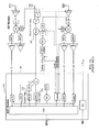
- In traditional radar embodiments, and with reference to Figure IA, a transmitter and a receiver are made up of discrete components. Single signal lines connect the individual components to each other and a digital signal processor (DSP)
module 110. Moreover, assembling discrete components results in an overall size increase in comparison to highly integrated circuit architecture. - Additionally, current narrowband frequency modulated continuous wave (FMCW) automotive radar products transmit a signal with a frequency ramp in discrete frequency steps. The discrete frequency steps are created using a digital-to-analog converter (DAC) integrated
circuit 154 to tune a free-running voltage controlled oscillator (VCO) 101. With reference toFigure 1B , the VCO 101 is typically built with a discrete GaAs FET and a discrete varactor diode. TheDAC 154 is typically located onDSP module 110 and an analog tuning voltage control signal is communicated from the DSP module to anRF module 105 containingVCO 101. However, traversing a board-to-board connection makes the analog tuning voltage control signal more susceptible to noise. The source of tuning noise may be aPWM 152,DAC 154, an adder or summing circuit, or interface induced noise. - In this typical architecture of a board-to-board connection,
DAC 154 is placed in close proximity to VCO 101 to limit noise coupling with the output ofDAC 154. However, the proximity of DAC 154 to VCO 101 should also be limited due to digital noise from the DAC programming lines. The balancing of these two limitations commonly results in isolation ofVCO 101 fromDAC 154 using metal compartments, again causing the system to be larger and more costly. - Typically, making an automotive radar product smaller has the result of worsening the isolation between transmit and receive signals. Nevertheless, a need exists for a more compact radar embodiment having improved isolation of transmit and receive signals. This invention addresses these needs and others.
- Various techniques may be implemented to isolate a receive signal from a transmit signal in an antenna. Signal isolation is desirable because it prevents interference of the signals with one another and minimizes signal noise, which reduces the signal quality. Some of the techniques are symmetry of at least two receive channels with regards to a transmit channel, using differential signals within the antenna, designing receive channel inputs to be orthogonal to a transmit channel, and designing a voltage controlled oscillator to be on the same substrate as the tuning circuitry of the voltage controlled oscillator.
- In an exemplary embodiment, a signal isolation system includes a transmit channel with an axis of symmetry, at least two receive channels, where the receive channels are substantially symmetrical about the transmit channel's access of symmetry. Designing a symmetrical layout of transmit and receive channels is configured to improve the signal isolation in the system. In another exemplary embodiment, differential signaling is used in the isolation system to communicate various signals. The differential signaling may be used in a portion, oi all of the receive and transmit channels.
- In another exemplary embodiment, the tuning circuitry for a voltage controlled oscillator is placed on the MMIC, instead of a DSP as is typically done. Interference noise is reduced by using digital control signals between the DSP and tuning circuitry.
-
-
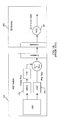
FIGS. 1A-1B show examples of a prior art schematic of a discrete transceiver circuit; -
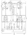
FIG. 2 shows an exemplary schematic of an integrated circuit utilizing differential signaling; -
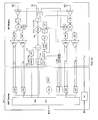
FIGS. 3A-3B show examples of an integrated voltage controlled oscillator tuning architecture; -
FIG. 4 shows an example of a symmetric integrated circuit layout; -
FIG. 5 shows an exemplary PCB and MMIC layout; and -
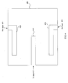
FIG. 6 shows a graphical representation of the signal isolation in an exemplary embodiment. - While exemplary embodiments are described herein in sufficient detail to enable those skilled in the art to practice the invention, it should be understood that other embodiments may be realized and that logical electrical and mechanical changes may be made without departing from the spirit and scope of the invention. Thus, the following detailed description is presented for purposes of illustration only.
- In accordance with an exemplary embodiment, a first technique for providing improved isolation of transmit and receive signals comprises the use of differential signal communication. In accordance with an exemplary embodiment, and with reference to
Figure 2 , an integrated circuit (IC), such as a monolithic microwave integrated circuit (MMIC) 299 is located on a printed circuit board (PCB) 298, and is in communication with a digital signal processor (DSP)module 297. In an exemplary embodiment, MMIC 299 comprises atransmit channel 230, a first receivechannel 231, and a second receivechannel 232. More specifically, in an exemplary embodiment, transmitchannel 230 comprises atransmit output node 290, a Balun 291, asplitter 215, and aVCO 201 in communication with tuning circuitry on theDSP module 297. Accordingly, transmitoutput node 290 is in communication with Balun 291 outside of MMIC 299, which in turn is in communication withsplitter 215 and VCO 201. VCO 201 receives at least one signal from the tuning circuitry onDSP module 297. Furthermore, in the exemplary embodiment, first andsecond receive channels receive input node 260, a Balun 261, an LNA 216, asplitter 215, amixer 212, a filter (or band pass filter) 220, and anamplifier 221. Receiveinput node 260 is in communication with Balun 261, which communicates a receive signal to LNA 216,splitter 215, and then to mixer 212. The receive signal is further communicated frommixer 212 to filter 220 andamplifier 221 before being transmitted toDSP module 297. - Isolation of the transmit and receive signals increases in response to transmitting signals using differential signaling. In accordance with an exemplary embodiment, the transmission path from receive output node(s) 269 to Balun 261 is configured for differential signal communication. In another exemplary embodiment, at least a portion of the receive channel is configured for differential signal mode communication of the receive signal. For example, the portion of the recerve channel between
power splitter 215 and Balun 261 may be configured for differential signal communication. In another example, differential signaling is present from Balun 261 tomixer 212. In another exemplary embodiment, differential signaling is present from Balun 261 to filter 220. In yet another exemplary embodiment, the portion of the transmission path frommixer 212 to receive output node(s) 269 is configured for differential signal communication - In accordance with an exemplary embodiment, transmit
channel 230 is configured to transmit a signal using differential signaling, from atransmit input node 289 to Balun 291. In another exemplary embodiment, at least a portion of transmitchannel 230 is configured for differential signal communication of the transmit signal. For example, the transmission path between VCO 201 and Balun 291 may be configured for differential signalling. In another example, the portion of the transmission path betweenpower splitter 215 and Balun 291 may be configured for differential signalling. - Thus, in accordance with various aspects of the present invention, the radar product is designed to implement both the receiver channels and the transmitter channel on the same MMIC. This tends to reduce the size and cost of the RF module, and consequently the overall system. Moreover, implementing both the receiver channels and the transmitter channel on the same MMIC facilitates an improvement in transmitter-to-receiver isolation, relative to a comparable device that does not employ differential signaling. Furthermore, although described herein in the context of a MMIC, in other exemplary embodiments, the components described herein may be discrete components because the implementation of similar differential signaling may be advantageous in a discrete component configuration.
- In an exemplary embodiment and as illustrated by the graph of
Figure 6 , the use of differential signaling, in either a MMIC embodiment or a discrete component embodiment, improves the transmitter-to-recciver isolation by approximately 15 dB or greater relative to a similar RF module that does not use differential signalling. In other exemplary embodiments, the transmitter-to-receiver isolation improvement is 5 dB to 25 dB or more, in comparison to a similar RF module that uses single-ended signalling. In one exemplary embodiment, an absolute isolation of 45 - 55 dB is possible, which compares to a signal isolation of 30 - 40 dB in a similar RF module not using differential signalling. - Using differential signaling aids in controlling the interference between components. In accordance with an exemplary embodiment, differential signaling is accomplished by communicating complementary signals through at least two separate wires and then comparing the complementary signals. The radiation of electromagnetic energy is also reduced because the current in one line is equal and opposite of the current in the other differential line. In general, differential signaling improves isolation of the communicated signal by supporting removal of noise.
- In an exemplary embodiment, various factors are configured to reduce interference between components, such as, the distance between the differential wires, and the length and/or diameter of the differential wires, and the frequency of the transmitted signal.
- The spacing between the differential signal lines is small compared to the spacing between transmit and receive channels, therefore an equal amount of electromagnetic energy is imparted on both differential lines. The electromagnetic energy can be eliminated in the amplification stage if the voltage difference between the lines is amplified. In an exemplary embodiment, the longer the coupled lines, the better the signal isolation. Moreover, a transmission line effect is realized as the relationship between the signal frequency and the length of the coupled lines increases.
- The isolation benefit of facilitating differential signaling increases as the transmitted signal frequency increases. In other words, the benefit is higher at high frequencies in comparison to low frequencies. In an exemplary embodiment, such isolation benefits are realized at signal frequencies exceeding 3 GHz. In another exemplary embodiment, isolation benefits are realized at signal frequencies exceeding 10 GHz.
- In accordance with another exemplary embodiment, a second technique for providing improved isolation of transmit and receive signals comprises the use of symmetry. In an exemplary embodiment, and with reference to
Figure 4 , aMMIC 400 includes a transmitchannel 410, a first receivechannel 420, and a second receivechannel 430. Furthermore, in the exemplary embodiment, transmitchannel 410 has at least one axis of symmetry, with transmitchannel 410 being symmetrical about the transmitter axis. The axis of symmetry, for example, may be along the transmit channel. - Various configurations of the transmit and receive channels are possible. In an exemplary embodiment, receive
channels channels channels - Furthermore, in an exemplary embodiment, receive
channels channel 420 and the corresponding point of second receivechannel 430 are equidistant from the transmitter axis. - In accordance with an exemplary embodiment, the symmetry between transmit
channel 410 and receivechannels channel 410 and receivechannels Figure 6 , signal isolation is highest as the receive signals' amplitude and phase cancel each other. However, increases in the pairs of receive channel points that are symmetrical results in higher signal isolation benefit, though not all receive channel points have an equal effect on isolation - In an exemplary embodiment, the portions of the receive channels where the receive signal frequency is identical, or approximately the same, to the transmit signal frequency are the portions where a symmetrical configuration yields the most benefit for signal isolation. The receive signal frequency and the transmit signal frequency are considered approximately the same if the two frequencies are within 10% of each other. For example, if the transmit signal frequency is 20 GHz, then a receive signal frequency in the range of 18 GHz to 22 GHz is approximately the same for improved signal isolation using symmetry.
- With momentary reference to
Figure 4 , an example of such a receive channel portion is aninput portion 425 of first receivechannel 420, and aninput portion 435 of second receivechannel 430. In an exemplary embodiment, the input portion of a receiver channel is the portion from the receiver input node to the associated Balun, where the received signal is converted to a differential signal. Thus, in an exemplary embodiment, the input portions of the receive channels are configured symmetrically about the transmit channel. - Another important area of symmetry exists where a signal is transmitted in a single line as opposed to a differential signal. Thus, it is beneficial to design a layout such that portions comprising a single line are symmetric. Furthermore, in an exemplary embodiment, differential signaling and symmetry are used in areas of a MMIC where the receive signals and the transmit signal are communicated at similar frequencies, for example at the final carrier frequency.
- A MMIC configured with two receivers placed equal distances from the transmitter results in system improvement because the leakage to both receivers will be nearly identical and therefore more easily removed in subsequent signal processing. The larger the difference between the absolute distance from the transmit channel to a first receive channel in comparison to the absolute distance from the transmit channel to a second receive channel, the more difficult is it to remove signal leakage. This relationship can be described as (Tx - Rxi : Tx - Rx2). Thus, as the asymmetry of the layout increases, the isolation benefit decreases. In an exemplary embodiment, a beneficial signal isolation is 40 dB or higher.
- In accordance with another exemplary embodiment and with continued reference to
Figure 4 , a third technique for providing improved signal isolation comprises designing first receiveinput 425 and second receiveinput 435 approximately orthogonally orientated to transmitinput 415. Designing first and second receiveinputs input 415, reduces the electrical field interference of the receive inputs and transmit input with each other. Although illustrated in block format inFigure 4 , examples of the aforementioned symmetry can also be seen inFigure 5 , where the receive channels are communicated to the MMIC at approximately 90 degrees from the transmit channel. - In accordance with another exemplary embodiment, a fourth technique for providing improved isolation of transmit and receive signals comprises designing a tuning circuit on an integrated circuit for tuning a VCO. With reference to
Figure 1B , in the prior art, one manner of tuning aVCO 101 involves VCO tuning circuitry onDSP module 110 comprising a pulse width modulator (PWM) 152 andDAC 154. In accordance with an exemplary embodiment, this tuning function is moved on-chip. In the exemplary embodiment, and with reference toFigure 3A-3B , the tuning circuitry providing a tuning voltage to a VCO and a VCO are integrated on the same printed circuit board. In another exemplary embodiment, a VCO tuning circuitry and a VCO are integrated in a radar embodiment of aMMIC 399. - In an exemplary embodiment, VCO tuning circuitry includes a pulse width modulator (PWM) 352 and a
DAC 354. The VCO tuning circuitry may also comprise a low-pass filter (LPF) 356.PWM 352 connects to aDSP 310 and receives a digital signal as an input signal. The output ofPWM 352 connects to aVCO 301 andPWM 352 is configured to control the coarse tuning portion of the VCO tuning circuitry. In an exemplary embodiment,PWM 352 comprises a group of parallel capacitors with switches to adjust resonant frequency and is configured to perform coarse tuning on-chip. Furthermore, any suitable device(s) that perform coarse tuning on-chip may be used. - In one embodiment,
DAC 354 also connects toDSP 310 and receives a digital signal as an input signal. The output ofDAC 354 is in communication withVCO 301 andDAC 354 is configured to control the fine tuning portion of the VCO tuning circuitry. In another exemplary embodiment,DAC 354 comprises a varactor diode and is configured is control the fine tuning accomplished by adjusting a varactor diode voltage supplied byDAC 354. Furthermore, in an exemplary embodiment,DAC 354 is isolated fromVCO 301 by n-wells. - In accordance with an exemplary embodiment, designing a digital interface by placing the VCO tuning circuitry on-chip improves the chip performance by reducing the susceptibility of the VCO tuning voltage to noise at the transmission interface. In an exemplary embodiment and in contrast to the prior art, the source of tuning noise is no longer
PWM 352, an adder or summing circuit, or any interface induced noise. The remaining source of tuning noise isDAC 354. The VCO is less susceptible to tuning noise because the transmit signal can remain digital as it moves from board-to-board. Thus, in an exemplary embodiment, VCO tuning control signals are communicated toMMIC 399 in a digital signal form. - Furthermore, in accordance with an exemplary embodiment, signal interference due to tuning is further reduced in response to the digital VCO tuning control signal being turned off when not used, in comparison to a continuous analog signal. Since
VCO 301 is not continuously tuned, the digital VCO tuning control signal does not need to be continuously transmitted. In other words, in an exemplary embodiment, the digital VCO tuning control signal is received atVCO 301 in a non-continuous or periodic manner. If the digital VCO tuning control signal is not transmitted, the possibility of signal interference with at least one of the transmit signal or the receive signal(s) is reduced. - In an exemplary embodiment, no filter is present between
DSP 310 andDAC 354 located onMMIC 399. In the exemplary embodiment, the use of digital signals does not require filtering, and signals are transmitted fromDSP 310 toMMIC 399 faster than analog signals that are filtered onDSP 310 before transmission toMMIC 399. In another exemplary embodiment,DSP 310 can chirp signals without any latency effect from transmission. A chirp is a signal in which the frequency increases or decreases with time, and is a well-known concept in the art. - In an exemplary embodiment, and with reference to
Figure 5 , an IC phase noise performance and receiver balance are greatly improved due to implementing multiple transmit, receive, and frequency tuning techniques in a single IC. In an exemplary embodiment, the techniques include at least one of using differential signaling, designing a symmetrical layout of a transmitter and two receivers, designing the receive channel inputs to be orthogonal to the transmit channel, and integrating VCO tuning circuitry on the same IC as a VCO. By using at least one of these techniques, an IC may be configured to reduce signal interference and operate more effectively. -
Figure 5 illustrates an exemplary printed circuit board layout and some of the various techniques described above. For example, aMMIC 501 communicates with a transmitportion 502, and two receive portions 503, 504. The signals passing through transmitportion 502 and receive portions 503, 504 are communicated in part usingdifferential signaling 519 betweenMMIC 501 and Baluns 512-514. Furthermore,Figure 5 illustrates the receive inputs ofMMIC 501 configured orthogonally to the transmit input. - Benefits, other advantages, and solutions to problems have been described above with regard to specific embodiments. However, the benefits, advantages, solutions to problems, and any element(s) that may cause any benefit, advantage, or solution to occur or become more pronounced are not to be construed as critical, required, or essential features or elements of any or all the claims. As used herein, the terms "includes," "including," "comprises," "comprising," or any other variation thereof, are intended to cover a nonexclusive inclusion, such that a process, method, article, or apparatus that comprises a list of elements does not include only those elements but may include other elements not expressly listed or inherent to such process, method, article, or apparatus. Further, no element described herein is required for the practice of the invention unless expressly described as "essential" or "critical".
The following numbered paragraphs set out further aspects of the present disclosure: - 1. A radio frequency (RP) signal isolation system comprising:
- a transmit channel with an axis of symmetry;
- at least two receive channels configured to communicate receive signals at approximately the same frequency; and
- wherein the at least two receive channels are substantially symmetrical about the axis of symmetry of the transmit channel; and
- wherein the signal isolation system is configured to isolate the receive signals from a transmit signal based at least in part on the symmetry of the at least two receive channels.
- 2. The system of
paragraph 1, wherein the system is a monolithic microwave integrated circuit (MMIC), and wherein the system is part of a radar system. - 3. The system of
paragraph 1, wherein the entirety of the at least two receive channels are substantially symmetrical about the axis of symmetry of the transmit channel, and wherein the axis of symmetry is along the transmit channel. - 4. The system of
paragraph 1, wherein the at least two receive channels individually comprise an input portion and each input portion of the at least two receive channels are substantially symmetrical about the axis of symmetry of the transmit channel, and wherein signal isolation of the receive signals increases as the symmetry of the at least two receive channels increases. - 5. The system of
paragraph 1, further comprising a pair of differential conductors in at least a portion of each of the at least two receive channels, wherein the at least two receive channels are configured to transmit a differential signal. - 6. The system of paragraph 5, wherein substantially all of the at least two receive channels comprise the pair of differential conductors.
- 7. The system of paragraph 5, wherein the at least a portion of each of the at least two receive channels includes portions of the receive channels, wherein a receive signal frequency is substantially the same as a transmit signal frequency.
- 8. The system of
paragraph 1, wherein the at least two receive channels individually further comprise a receive input node approximately orthogonal to the axis of symmetry of the transmit channel. - 9. A signal isolation system comprising:
- a transmit channel;
- at least two receive channels; and
- a pair of differential conductors in at least a portion of each of the at least two receive channels, wherein the at least two receive channels are configured to transmit a differential signal.
- 10. The signal isolation system of paragraph 9, further comprising a pair of differential conductors in at least a portion of the transmit channel, wherein the transmit channel is configured to transmit a differential signal.
- 11. The signal isolation system of paragraph 9, wherein the transmit channel and the at least two receive channels are part of a monolithic microwave integrated circuit.
- 12. An integrated circuit comprising a transmit channel with an axis of symmetry, two receiver channels, and wherein at least one of the transmit channel and the two receive channels at least partially comprise coupled differential lines communicating a differential signal, wherein the two receiver channels are spaced symmetrically about the axis of symmetry of the transmitter channel.
- 13. The integrated circuit of
paragraph 12, wherein the plurality of coupled differential lines provides isolation of 40 dB or more between a transmit signal and a receive signal. - 14. The integrated circuit of
paragraph 12, wherein the integrated circuit is a monolithic microwave integrated circuit. - 15. The integrated circuit of
paragraph 12, wherein the two receiver channels individually comprise a receiver input that is approximately orthogonal with the axis of symmetry of the transmitter channel, and wherein the axis of symmetry of the transmit channel is along the length of the transmitter. - 16. The integrated circuit of
paragraph 12, further comprising:- a voltage-controlled oscillator (VCO); and
- a VCO tuning circuit comprising:
- a pulse-width modulator (PWM) configured to provide coarse tuning of the VCO; and
- a digital-to-analog converter (DAC) configured to provide fine tuning of the VCO;
- wherein the VCO tuning circuit receives a digital tuning control signal from a digital signal processor.
- 17. A voltage-controlled oscillator (VCO) tuning circuit comprising:
- a pulse-width modulator (PWM) configured to provide coarse tuning of a CO;
- a digital-to-analog converter (DAC) configured to provide fine tuning of the VCO;
- wherein the VCO, the PWM, and the DAC are located on a substrate of an integrated circuit; and
- wherein the VCO tuning circuit receives a digital tuning control signal from a digital signal processor that is not located on the same substrate as the VCO.
- 18. The VCO tuning circuit of paragraph 17, further comprising n-wells to isolate the DAC from the VCO, and wherein the DAC is a varactor diode.
- 19. The VCO tuning circuit of paragraph 17, wherein the digital tuning control signal is a non-continuous digital input signal, and wherein the digital signal processor is configured to chirp the digital tuning control signal without substantial latency.
- 20. The VCO tuning circuit of paragraph 17, wherein the integrated circuit is at least one of a MMIC and a radar chip.
Claims (7)
- A voltage-controlled oscillator (VCO) tuning circuit comprising:a pulse-width modulator (PWM) configured to provide coarse tuning of a voltage-controlled oscillator (VCO);a digital-to-analog converter (DAC) configured to provide fine tuning of the VCO;wherein the VCO, the PWM, and the DAC are located on a substrate of an integrated circuit; andwherein the VCO tuning circuit receives a digital tuning control signal from a digital signal processor that is not located on the same substrate as the VCO.
- The VCO tuning circuit of claim 1, further comprising n-wells to isolate the DAC from the VCO, and wherein the DAC drives a varactor diode.
- The VCO tuning circuit of any preceding claim, wherein the digital tuning control signal is a non-continuous digital input signal, and wherein the digital signal processor is configured to chirp the digital tuning control signal without substantial latency.
- The VCO tuning circuit of any preceding claim, wherein the integrated circuit is at least one of a MMIC and a radar chip.
- The VCO tuning circuit of any preceding claim, wherein the integrated circuit comprises:a transmit channel with an axis of symmetry;two receiver channels; andwherein at least one of the transmit channel and the two receive channels at least partially comprise coupled differential lines communicating a differential signal;wherein the two receiver channels are spaced symmetrically about the axis of symmetry of the transmitter channel.
- The VCO tuning circuit of claim 5, wherein the plurality of coupled differential lines provides isolation of 40 dB or more between a transmit signal and a receive signal.
- The VCO tuning circuit of claim 5 or claim 6, wherein the two receiver channels individually comprise a receiver input that is approximately orthogonal with the axis of symmetry of the transmitter channel, and wherein the axis of symmetry of the transmit channel is along the length of the transmitter.
Applications Claiming Priority (3)
| Application Number | Priority Date | Filing Date | Title |
|---|---|---|---|
| US2555908P | 2008-02-01 | 2008-02-01 | |
| PCT/US2009/032670 WO2009099952A2 (en) | 2008-02-01 | 2009-01-30 | Highly integrated circuit architecture |
| EP09708419A EP2247958A2 (en) | 2008-02-01 | 2009-01-30 | Highly integrated circuit architecture |
Related Parent Applications (1)
| Application Number | Title | Priority Date | Filing Date |
|---|---|---|---|
| EP09708419A Division EP2247958A2 (en) | 2008-02-01 | 2009-01-30 | Highly integrated circuit architecture |
Publications (2)
| Publication Number | Publication Date |
|---|---|
| EP2762913A1 true EP2762913A1 (en) | 2014-08-06 |
| EP2762913B1 EP2762913B1 (en) | 2018-11-21 |
Family
ID=40672313
Family Applications (3)
| Application Number | Title | Priority Date | Filing Date |
|---|---|---|---|
| EP14163942.7A Active EP2762913B1 (en) | 2008-02-01 | 2009-01-30 | Highly integrated circuit architecture |
| EP09707492.6A Active EP2247959B1 (en) | 2008-02-01 | 2009-01-30 | Integrated frequency calibration architecture |
| EP09708419A Withdrawn EP2247958A2 (en) | 2008-02-01 | 2009-01-30 | Highly integrated circuit architecture |
Family Applications After (2)
| Application Number | Title | Priority Date | Filing Date |
|---|---|---|---|
| EP09707492.6A Active EP2247959B1 (en) | 2008-02-01 | 2009-01-30 | Integrated frequency calibration architecture |
| EP09708419A Withdrawn EP2247958A2 (en) | 2008-02-01 | 2009-01-30 | Highly integrated circuit architecture |
Country Status (3)
| Country | Link |
|---|---|
| US (2) | US8044845B2 (en) |
| EP (3) | EP2762913B1 (en) |
| WO (2) | WO2009099953A1 (en) |
Cited By (1)
| Publication number | Priority date | Publication date | Assignee | Title |
|---|---|---|---|---|
| US20130082869A1 (en) * | 2011-09-29 | 2013-04-04 | Herbert Jaeger | Radar circuit, radar system and method for testing |
Families Citing this family (42)
| Publication number | Priority date | Publication date | Assignee | Title |
|---|---|---|---|---|
| EP2762913B1 (en) * | 2008-02-01 | 2018-11-21 | ViaSat Inc. | Highly integrated circuit architecture |
| WO2010092438A1 (en) | 2009-02-13 | 2010-08-19 | Freescale Semiconductor, Inc. | Integrated circuit comprising frequency generation circuitry for controlling a frequency source |
| US8604888B2 (en) * | 2009-12-23 | 2013-12-10 | Sand 9, Inc. | Oscillators having arbitrary frequencies and related systems and methods |
| US8704604B2 (en) * | 2009-12-23 | 2014-04-22 | Sand 9, Inc. | Oscillators having arbitrary frequencies and related systems and methods |
| US8736388B2 (en) * | 2009-12-23 | 2014-05-27 | Sand 9, Inc. | Oscillators having arbitrary frequencies and related systems and methods |
| JP5307067B2 (en) * | 2010-03-30 | 2013-10-02 | 古河電気工業株式会社 | Automotive pulse radar |
| DE102012100427A1 (en) * | 2012-01-19 | 2013-07-25 | Hella Kgaa Hueck & Co. | Device with a voltage-controlled oscillator and a circuit arrangement for driving the oscillator |
| DE102012106506A1 (en) * | 2012-07-18 | 2014-01-23 | Hella Kgaa Hueck & Co. | Method for determining the functionality of a switchable receive amplifier |
| US20140027157A1 (en) * | 2012-07-26 | 2014-01-30 | Futurewei Technologies, Inc. | Device and Method for Printed Circuit Board with Embedded Cable |
| CN102915067B (en) * | 2012-10-30 | 2014-08-06 | 中国科学技术大学 | High-precision bias voltage control equipment and direct current stabilized voltage power supply |
| TWI486611B (en) * | 2013-04-18 | 2015-06-01 | Wistron Neweb Corp | Radar device for an automotive radar system |
| CN104122556B (en) * | 2013-04-24 | 2017-08-15 | 启碁科技股份有限公司 | Radar apparatus for vehicle radar system |
| US9488719B2 (en) * | 2014-05-30 | 2016-11-08 | Toyota Motor Engineering & Manufacturing North America, Inc. | Automotive radar sub-system packaging for robustness |
| US9685960B2 (en) * | 2014-07-31 | 2017-06-20 | Valeo Radar Systems, Inc. | Method and apparatus for generating a bit stream signal having a reduced output swing |
| TWI540787B (en) | 2014-12-09 | 2016-07-01 | 啟碁科技股份有限公司 | Balun filter and radio-frequency system |
| CN105742763B (en) * | 2014-12-11 | 2019-01-01 | 启碁科技股份有限公司 | balun filter and radio frequency system |
| DE102015103149B4 (en) * | 2015-03-04 | 2024-06-06 | HELLA GmbH & Co. KGaA | Radar device |
| DE102015107419A1 (en) * | 2015-05-12 | 2016-11-17 | HÜBNER GmbH & Co. KG | radar device |
| US10727848B2 (en) * | 2015-07-08 | 2020-07-28 | Analog Devices Global | Phase-locked loop having a multi-band oscillator and method for calibrating same |
| WO2017175190A1 (en) * | 2016-04-07 | 2017-10-12 | Uhnder, Inc. | Adaptive transmission and interference cancellation for mimo radar |
| US10261179B2 (en) | 2016-04-07 | 2019-04-16 | Uhnder, Inc. | Software defined automotive radar |
| US9846228B2 (en) | 2016-04-07 | 2017-12-19 | Uhnder, Inc. | Software defined automotive radar systems |
| US10069465B2 (en) | 2016-04-21 | 2018-09-04 | Communications & Power Industries Llc | Amplifier control system |
| EP3449275B1 (en) | 2016-04-25 | 2025-08-20 | Robert Bosch GmbH | Pmcw-pmcw interference mitigation |
| US9945935B2 (en) | 2016-04-25 | 2018-04-17 | Uhnder, Inc. | Digital frequency modulated continuous wave radar using handcrafted constant envelope modulation |
| EP3449272B1 (en) | 2016-04-25 | 2022-11-02 | Uhnder, Inc. | Vehicle radar system with a shared radar and communication system, and method for managing such a system in a vehicle |
| US9753121B1 (en) | 2016-06-20 | 2017-09-05 | Uhnder, Inc. | Power control for improved near-far performance of radar systems |
| US10295580B2 (en) | 2016-10-03 | 2019-05-21 | Analog Devices Global | On-chip measurement for phase-locked loop |
| WO2018146530A1 (en) | 2017-02-10 | 2018-08-16 | Uhnder, Inc. | Reduced complexity fft-based correlation for automotive radar |
| US11454697B2 (en) | 2017-02-10 | 2022-09-27 | Uhnder, Inc. | Increasing performance of a receive pipeline of a radar with memory optimization |
| US9971020B1 (en) | 2017-02-10 | 2018-05-15 | Uhnder, Inc. | Radar data buffering |
| US11105890B2 (en) | 2017-12-14 | 2021-08-31 | Uhnder, Inc. | Frequency modulated signal cancellation in variable power mode for radar applications |
| US12386029B2 (en) | 2018-01-29 | 2025-08-12 | Robert Bosch Gmbh | Millimeter wave automotive radar systems |
| US11474225B2 (en) | 2018-11-09 | 2022-10-18 | Uhnder, Inc. | Pulse digital mimo radar system |
| DE102019103514A1 (en) * | 2019-02-12 | 2020-08-13 | Infineon Technologies Ag | Processing of radar signals |
| US11681017B2 (en) | 2019-03-12 | 2023-06-20 | Uhnder, Inc. | Method and apparatus for mitigation of low frequency noise in radar systems |
| WO2021144710A2 (en) | 2020-01-13 | 2021-07-22 | Uhnder, Inc. | Method and system for multi-chip operation of radar systems |
| EP3903413B1 (en) * | 2020-02-20 | 2022-03-30 | 2pi-Labs GmbH | Reference oscillator arrangement, radar system and synchronisation method |
| US11251822B1 (en) * | 2020-07-23 | 2022-02-15 | Xilinx, Inc. | Software defined radio (SDR) filter relaxation technique for multiple-input and multiple-output (MIMO) and large antenna array (LAA) applications |
| US12498452B2 (en) | 2021-12-02 | 2025-12-16 | Robert Bosch Gmbh | Radar system with enhanced processing for increased contrast ratio, improved angular separability and accuracy, and elimination of ghost targets in a single-snapshot |
| CN114630511B (en) * | 2022-03-04 | 2024-03-19 | 中国航天科工集团八五一一研究所 | An implementation method of two-way frequency conversion integrated components |
| US20240192314A1 (en) * | 2022-12-08 | 2024-06-13 | Stmicroelectronics International N.V. | Method and apparatus for reducing storage for proportional data |
Citations (3)
| Publication number | Priority date | Publication date | Assignee | Title |
|---|---|---|---|---|
| WO2007086502A1 (en) * | 2006-01-26 | 2007-08-02 | Nihon Dempa Kogyo Co., Ltd. | Vco driving circuit and frequency synthesizer |
| JP2007267375A (en) * | 2006-02-28 | 2007-10-11 | Nippon Dempa Kogyo Co Ltd | Oscillator and frequency synthesizer |
| US20080001810A1 (en) * | 2006-05-24 | 2008-01-03 | Johann Peter Forstner | Integrated Multi-Mixer Circuit |
Family Cites Families (22)
| Publication number | Priority date | Publication date | Assignee | Title |
|---|---|---|---|---|
| US3618091A (en) * | 1961-11-10 | 1971-11-02 | Sanders Associates Inc | Conical antenna system |
| US3452300A (en) * | 1965-08-11 | 1969-06-24 | Merrimac Research & Dev Inc | Four port directive coupler having electrical symmetry with respect to both axes |
| US3803514A (en) * | 1972-06-05 | 1974-04-09 | Cayuga Ass Inc | Microwave oscillator |
| DE3526363A1 (en) * | 1985-07-19 | 1987-01-22 | Siemens Ag | METHOD FOR PRODUCING AN ADJUSTABLE FREQUENCY GENERATOR |
| US4791421A (en) * | 1986-09-10 | 1988-12-13 | Westinghouse Electric Corp. | Transmit-receive module for phased-array antennas |
| US5262957A (en) | 1990-11-09 | 1993-11-16 | Global Communications, Inc. | Inexpensive portable RF spectrum analyzer with calibration features |
| DE69729344T8 (en) | 1996-04-03 | 2005-02-17 | Honda Giken Kogyo K.K. | Radar module and MMIC arrangement for it |
| AU2147900A (en) * | 1998-11-12 | 2000-05-29 | Broadcom Corporation | Fully integrated tuner architecture |
| US6696898B1 (en) * | 1998-11-12 | 2004-02-24 | Broadcom Corporation | Differential crystal oscillator |
| US7113744B1 (en) * | 1999-10-21 | 2006-09-26 | Broadcom Corporation | Adaptive radio transceiver with a power amplifier |
| US7555263B1 (en) * | 1999-10-21 | 2009-06-30 | Broadcom Corporation | Adaptive radio transceiver |
| US7299006B1 (en) * | 1999-10-21 | 2007-11-20 | Broadcom Corporation | Adaptive radio transceiver |
| US6987966B1 (en) * | 1999-10-21 | 2006-01-17 | Broadcom Corporation | Adaptive radio transceiver with polyphase calibration |
| US6549078B1 (en) | 2000-11-18 | 2003-04-15 | Ashvattha Semiconductor Inc. | Method and system for directly modulating a voltage controlled oscillator for use in frequency/phase modulated systems |
| US7148683B2 (en) * | 2001-10-25 | 2006-12-12 | Intematix Corporation | Detection with evanescent wave probe |
| US7183922B2 (en) * | 2002-03-18 | 2007-02-27 | Paratek Microwave, Inc. | Tracking apparatus, system and method |
| US6838963B2 (en) * | 2002-04-01 | 2005-01-04 | Med-El Elektromedizinische Geraete Gmbh | Reducing effects of magnetic and electromagnetic fields on an implant's magnet and/or electronics |
| US8222721B2 (en) * | 2003-09-15 | 2012-07-17 | Silicon Laboratories Inc. | Integrated circuit suitable for use in radio receivers |
| KR20080051180A (en) | 2005-09-23 | 2008-06-10 | 캘리포니아 인스티튜트 오브 테크놀로지 | A mm-wave fully integrated phased array receiver and transmitter with on chip antennas |
| DE102006024457B4 (en) * | 2006-05-24 | 2014-06-05 | Infineon Technologies Ag | Integrated circuit for transmitting and / or receiving signals |
| US7573420B2 (en) * | 2007-05-14 | 2009-08-11 | Infineon Technologies Ag | RF front-end for a radar system |
| EP2762913B1 (en) * | 2008-02-01 | 2018-11-21 | ViaSat Inc. | Highly integrated circuit architecture |
-
2009
- 2009-01-30 EP EP14163942.7A patent/EP2762913B1/en active Active
- 2009-01-30 EP EP09707492.6A patent/EP2247959B1/en active Active
- 2009-01-30 WO PCT/US2009/032672 patent/WO2009099953A1/en not_active Ceased
- 2009-01-30 US US12/363,412 patent/US8044845B2/en active Active
- 2009-01-30 US US12/363,436 patent/US7804369B2/en active Active
- 2009-01-30 EP EP09708419A patent/EP2247958A2/en not_active Withdrawn
- 2009-01-30 WO PCT/US2009/032670 patent/WO2009099952A2/en not_active Ceased
Patent Citations (3)
| Publication number | Priority date | Publication date | Assignee | Title |
|---|---|---|---|---|
| WO2007086502A1 (en) * | 2006-01-26 | 2007-08-02 | Nihon Dempa Kogyo Co., Ltd. | Vco driving circuit and frequency synthesizer |
| JP2007267375A (en) * | 2006-02-28 | 2007-10-11 | Nippon Dempa Kogyo Co Ltd | Oscillator and frequency synthesizer |
| US20080001810A1 (en) * | 2006-05-24 | 2008-01-03 | Johann Peter Forstner | Integrated Multi-Mixer Circuit |
Cited By (4)
| Publication number | Priority date | Publication date | Assignee | Title |
|---|---|---|---|---|
| US20130082869A1 (en) * | 2011-09-29 | 2013-04-04 | Herbert Jaeger | Radar circuit, radar system and method for testing |
| US9019154B2 (en) * | 2011-09-29 | 2015-04-28 | Infineon Technologies Ag | Radar circuit, radar system and method for testing |
| US20150234037A1 (en) * | 2011-09-29 | 2015-08-20 | Herbert Jaeger | Radar circuit, radar system and method for testing |
| US10094913B2 (en) * | 2011-09-29 | 2018-10-09 | Infineon Technology Ag | Radar circuit, radar system and method for testing |
Also Published As
| Publication number | Publication date |
|---|---|
| EP2762913B1 (en) | 2018-11-21 |
| WO2009099952A3 (en) | 2009-10-15 |
| US7804369B2 (en) | 2010-09-28 |
| US20090195321A1 (en) | 2009-08-06 |
| EP2247958A2 (en) | 2010-11-10 |
| WO2009099952A2 (en) | 2009-08-13 |
| EP2247959A1 (en) | 2010-11-10 |
| US8044845B2 (en) | 2011-10-25 |
| WO2009099953A1 (en) | 2009-08-13 |
| US20090195440A1 (en) | 2009-08-06 |
| EP2247959B1 (en) | 2014-03-26 |
Similar Documents
| Publication | Publication Date | Title |
|---|---|---|
| EP2762913B1 (en) | Highly integrated circuit architecture | |
| EP1976134B1 (en) | Radio circuit arrangement with improved decoupling | |
| US11349506B2 (en) | Radio frequency module and communication device | |
| US10305533B2 (en) | Semiconductor device | |
| US6366166B1 (en) | Double pass band amplifier circuit and a radio frequency reception head | |
| US9143136B2 (en) | Pumped distributed wave oscillator system | |
| CN109196712B (en) | Magneto-inductive waveguide | |
| US6661306B2 (en) | Compact lumped element dual highpass/lowpass balun layout | |
| WO2021241233A1 (en) | Tracker module, power amplification module, high frequency module, and communication device | |
| US9379798B2 (en) | Modulation circuit for a radio device and a method thereof | |
| KR20230006509A (en) | Tracker module, power amplification module, high frequency module and communication device | |
| US7579929B2 (en) | Transmission circuit, antenna duplexer, and radio-frequency switch circuit | |
| US20090096532A1 (en) | Differential amplifier with single ended output | |
| WO2006099072A2 (en) | Radio frequency inductive-capacitive filter circuit topology | |
| EP3902146A1 (en) | Microwave receiver device | |
| KR20080108546A (en) | Receiving method, receiver, transceiver and integrated circuit in the transceiver | |
| JP2003282721A (en) | Semiconductor device and transmission / reception device | |
| US6693499B2 (en) | Compact lumped element ring balun layout | |
| CN113632374A (en) | power amplifier | |
| KR20010039546A (en) | Frequency-switching oscillator and electronic device using the same | |
| KR20060071388A (en) | Transceiver System for Millimeter Wave Band Using Patch Antenna | |
| WO2023009198A1 (en) | Passive class of modulators for mm-wave applications (5g/6g and radar) | |
| CN106487393A (en) | electronic device for use in a communication system | |
| NL2005607C2 (en) | A configurable communication device. | |
| JP2004023424A (en) | Power amplifier module |
Legal Events
| Date | Code | Title | Description |
|---|---|---|---|
| PUAI | Public reference made under article 153(3) epc to a published international application that has entered the european phase |
Free format text: ORIGINAL CODE: 0009012 |
|
| 17P | Request for examination filed |
Effective date: 20140408 |
|
| AC | Divisional application: reference to earlier application |
Ref document number: 2247958 Country of ref document: EP Kind code of ref document: P |
|
| AK | Designated contracting states |
Kind code of ref document: A1 Designated state(s): AT BE BG CH CY CZ DE DK EE ES FI FR GB GR HR HU IE IS IT LI LT LU LV MC MK MT NL NO PL PT RO SE SI SK TR |
|
| R17P | Request for examination filed (corrected) |
Effective date: 20150205 |
|
| RBV | Designated contracting states (corrected) |
Designated state(s): AT BE BG CH CY CZ DE DK EE ES FI FR GB GR HR HU IE IS IT LI LT LU LV MC MK MT NL NO PL PT RO SE SI SK TR |
|
| GRAP | Despatch of communication of intention to grant a patent |
Free format text: ORIGINAL CODE: EPIDOSNIGR1 |
|
| STAA | Information on the status of an ep patent application or granted ep patent |
Free format text: STATUS: GRANT OF PATENT IS INTENDED |
|
| RIC1 | Information provided on ipc code assigned before grant |
Ipc: H03L 7/08 20060101ALI20180522BHEP Ipc: H03C 3/09 20060101ALI20180522BHEP Ipc: G01S 7/40 20060101AFI20180522BHEP Ipc: H03L 7/099 20060101ALN20180522BHEP Ipc: H03L 7/10 20060101ALI20180522BHEP Ipc: G01S 7/03 20060101ALN20180522BHEP |
|
| INTG | Intention to grant announced |
Effective date: 20180612 |
|
| GRAS | Grant fee paid |
Free format text: ORIGINAL CODE: EPIDOSNIGR3 |
|
| GRAA | (expected) grant |
Free format text: ORIGINAL CODE: 0009210 |
|
| STAA | Information on the status of an ep patent application or granted ep patent |
Free format text: STATUS: THE PATENT HAS BEEN GRANTED |
|
| AC | Divisional application: reference to earlier application |
Ref document number: 2247958 Country of ref document: EP Kind code of ref document: P |
|
| AK | Designated contracting states |
Kind code of ref document: B1 Designated state(s): AT BE BG CH CY CZ DE DK EE ES FI FR GB GR HR HU IE IS IT LI LT LU LV MC MK MT NL NO PL PT RO SE SI SK TR |
|
| REG | Reference to a national code |
Ref country code: CH Ref legal event code: EP |
|
| REG | Reference to a national code |
Ref country code: IE Ref legal event code: FG4D |
|
| REG | Reference to a national code |
Ref country code: DE Ref legal event code: R096 Ref document number: 602009055857 Country of ref document: DE |
|
| REG | Reference to a national code |
Ref country code: AT Ref legal event code: REF Ref document number: 1068190 Country of ref document: AT Kind code of ref document: T Effective date: 20181215 |
|
| REG | Reference to a national code |
Ref country code: NL Ref legal event code: MP Effective date: 20181121 |
|
| REG | Reference to a national code |
Ref country code: AT Ref legal event code: MK05 Ref document number: 1068190 Country of ref document: AT Kind code of ref document: T Effective date: 20181121 |
|
| PG25 | Lapsed in a contracting state [announced via postgrant information from national office to epo] |
Ref country code: FI Free format text: LAPSE BECAUSE OF FAILURE TO SUBMIT A TRANSLATION OF THE DESCRIPTION OR TO PAY THE FEE WITHIN THE PRESCRIBED TIME-LIMIT Effective date: 20181121 Ref country code: LV Free format text: LAPSE BECAUSE OF FAILURE TO SUBMIT A TRANSLATION OF THE DESCRIPTION OR TO PAY THE FEE WITHIN THE PRESCRIBED TIME-LIMIT Effective date: 20181121 Ref country code: HR Free format text: LAPSE BECAUSE OF FAILURE TO SUBMIT A TRANSLATION OF THE DESCRIPTION OR TO PAY THE FEE WITHIN THE PRESCRIBED TIME-LIMIT Effective date: 20181121 Ref country code: LT Free format text: LAPSE BECAUSE OF FAILURE TO SUBMIT A TRANSLATION OF THE DESCRIPTION OR TO PAY THE FEE WITHIN THE PRESCRIBED TIME-LIMIT Effective date: 20181121 Ref country code: NO Free format text: LAPSE BECAUSE OF FAILURE TO SUBMIT A TRANSLATION OF THE DESCRIPTION OR TO PAY THE FEE WITHIN THE PRESCRIBED TIME-LIMIT Effective date: 20190221 Ref country code: BG Free format text: LAPSE BECAUSE OF FAILURE TO SUBMIT A TRANSLATION OF THE DESCRIPTION OR TO PAY THE FEE WITHIN THE PRESCRIBED TIME-LIMIT Effective date: 20190221 Ref country code: AT Free format text: LAPSE BECAUSE OF FAILURE TO SUBMIT A TRANSLATION OF THE DESCRIPTION OR TO PAY THE FEE WITHIN THE PRESCRIBED TIME-LIMIT Effective date: 20181121 Ref country code: ES Free format text: LAPSE BECAUSE OF FAILURE TO SUBMIT A TRANSLATION OF THE DESCRIPTION OR TO PAY THE FEE WITHIN THE PRESCRIBED TIME-LIMIT Effective date: 20181121 Ref country code: IS Free format text: LAPSE BECAUSE OF FAILURE TO SUBMIT A TRANSLATION OF THE DESCRIPTION OR TO PAY THE FEE WITHIN THE PRESCRIBED TIME-LIMIT Effective date: 20190321 |
|
| PG25 | Lapsed in a contracting state [announced via postgrant information from national office to epo] |
Ref country code: GR Free format text: LAPSE BECAUSE OF FAILURE TO SUBMIT A TRANSLATION OF THE DESCRIPTION OR TO PAY THE FEE WITHIN THE PRESCRIBED TIME-LIMIT Effective date: 20190222 Ref country code: PT Free format text: LAPSE BECAUSE OF FAILURE TO SUBMIT A TRANSLATION OF THE DESCRIPTION OR TO PAY THE FEE WITHIN THE PRESCRIBED TIME-LIMIT Effective date: 20190321 Ref country code: NL Free format text: LAPSE BECAUSE OF FAILURE TO SUBMIT A TRANSLATION OF THE DESCRIPTION OR TO PAY THE FEE WITHIN THE PRESCRIBED TIME-LIMIT Effective date: 20181121 Ref country code: SE Free format text: LAPSE BECAUSE OF FAILURE TO SUBMIT A TRANSLATION OF THE DESCRIPTION OR TO PAY THE FEE WITHIN THE PRESCRIBED TIME-LIMIT Effective date: 20181121 |
|
| PG25 | Lapsed in a contracting state [announced via postgrant information from national office to epo] |
Ref country code: IT Free format text: LAPSE BECAUSE OF FAILURE TO SUBMIT A TRANSLATION OF THE DESCRIPTION OR TO PAY THE FEE WITHIN THE PRESCRIBED TIME-LIMIT Effective date: 20181121 Ref country code: CZ Free format text: LAPSE BECAUSE OF FAILURE TO SUBMIT A TRANSLATION OF THE DESCRIPTION OR TO PAY THE FEE WITHIN THE PRESCRIBED TIME-LIMIT Effective date: 20181121 Ref country code: PL Free format text: LAPSE BECAUSE OF FAILURE TO SUBMIT A TRANSLATION OF THE DESCRIPTION OR TO PAY THE FEE WITHIN THE PRESCRIBED TIME-LIMIT Effective date: 20181121 Ref country code: DK Free format text: LAPSE BECAUSE OF FAILURE TO SUBMIT A TRANSLATION OF THE DESCRIPTION OR TO PAY THE FEE WITHIN THE PRESCRIBED TIME-LIMIT Effective date: 20181121 |
|
| REG | Reference to a national code |
Ref country code: DE Ref legal event code: R097 Ref document number: 602009055857 Country of ref document: DE |
|
| PG25 | Lapsed in a contracting state [announced via postgrant information from national office to epo] |
Ref country code: EE Free format text: LAPSE BECAUSE OF FAILURE TO SUBMIT A TRANSLATION OF THE DESCRIPTION OR TO PAY THE FEE WITHIN THE PRESCRIBED TIME-LIMIT Effective date: 20181121 Ref country code: SK Free format text: LAPSE BECAUSE OF FAILURE TO SUBMIT A TRANSLATION OF THE DESCRIPTION OR TO PAY THE FEE WITHIN THE PRESCRIBED TIME-LIMIT Effective date: 20181121 Ref country code: MC Free format text: LAPSE BECAUSE OF FAILURE TO SUBMIT A TRANSLATION OF THE DESCRIPTION OR TO PAY THE FEE WITHIN THE PRESCRIBED TIME-LIMIT Effective date: 20181121 Ref country code: RO Free format text: LAPSE BECAUSE OF FAILURE TO SUBMIT A TRANSLATION OF THE DESCRIPTION OR TO PAY THE FEE WITHIN THE PRESCRIBED TIME-LIMIT Effective date: 20181121 |
|
| REG | Reference to a national code |
Ref country code: CH Ref legal event code: PL |
|
| PLBE | No opposition filed within time limit |
Free format text: ORIGINAL CODE: 0009261 |
|
| STAA | Information on the status of an ep patent application or granted ep patent |
Free format text: STATUS: NO OPPOSITION FILED WITHIN TIME LIMIT |
|
| PG25 | Lapsed in a contracting state [announced via postgrant information from national office to epo] |
Ref country code: LU Free format text: LAPSE BECAUSE OF NON-PAYMENT OF DUE FEES Effective date: 20190130 |
|
| REG | Reference to a national code |
Ref country code: BE Ref legal event code: MM Effective date: 20190131 |
|
| 26N | No opposition filed |
Effective date: 20190822 |
|
| PG25 | Lapsed in a contracting state [announced via postgrant information from national office to epo] |
Ref country code: SI Free format text: LAPSE BECAUSE OF FAILURE TO SUBMIT A TRANSLATION OF THE DESCRIPTION OR TO PAY THE FEE WITHIN THE PRESCRIBED TIME-LIMIT Effective date: 20181121 |
|
| PG25 | Lapsed in a contracting state [announced via postgrant information from national office to epo] |
Ref country code: BE Free format text: LAPSE BECAUSE OF NON-PAYMENT OF DUE FEES Effective date: 20190131 |
|
| PG25 | Lapsed in a contracting state [announced via postgrant information from national office to epo] |
Ref country code: LI Free format text: LAPSE BECAUSE OF NON-PAYMENT OF DUE FEES Effective date: 20190131 Ref country code: CH Free format text: LAPSE BECAUSE OF NON-PAYMENT OF DUE FEES Effective date: 20190131 |
|
| PG25 | Lapsed in a contracting state [announced via postgrant information from national office to epo] |
Ref country code: TR Free format text: LAPSE BECAUSE OF FAILURE TO SUBMIT A TRANSLATION OF THE DESCRIPTION OR TO PAY THE FEE WITHIN THE PRESCRIBED TIME-LIMIT Effective date: 20181121 |
|
| PG25 | Lapsed in a contracting state [announced via postgrant information from national office to epo] |
Ref country code: MT Free format text: LAPSE BECAUSE OF NON-PAYMENT OF DUE FEES Effective date: 20190130 |
|
| PG25 | Lapsed in a contracting state [announced via postgrant information from national office to epo] |
Ref country code: CY Free format text: LAPSE BECAUSE OF FAILURE TO SUBMIT A TRANSLATION OF THE DESCRIPTION OR TO PAY THE FEE WITHIN THE PRESCRIBED TIME-LIMIT Effective date: 20181121 |
|
| PG25 | Lapsed in a contracting state [announced via postgrant information from national office to epo] |
Ref country code: HU Free format text: LAPSE BECAUSE OF FAILURE TO SUBMIT A TRANSLATION OF THE DESCRIPTION OR TO PAY THE FEE WITHIN THE PRESCRIBED TIME-LIMIT; INVALID AB INITIO Effective date: 20090130 |
|
| PG25 | Lapsed in a contracting state [announced via postgrant information from national office to epo] |
Ref country code: MK Free format text: LAPSE BECAUSE OF FAILURE TO SUBMIT A TRANSLATION OF THE DESCRIPTION OR TO PAY THE FEE WITHIN THE PRESCRIBED TIME-LIMIT Effective date: 20181121 |
|
| P01 | Opt-out of the competence of the unified patent court (upc) registered |
Effective date: 20230529 |
|
| PGFP | Annual fee paid to national office [announced via postgrant information from national office to epo] |
Ref country code: GB Payment date: 20260127 Year of fee payment: 18 |
|
| PGFP | Annual fee paid to national office [announced via postgrant information from national office to epo] |
Ref country code: IE Payment date: 20260127 Year of fee payment: 18 Ref country code: DE Payment date: 20260128 Year of fee payment: 18 |
|
| PGFP | Annual fee paid to national office [announced via postgrant information from national office to epo] |
Ref country code: FR Payment date: 20260126 Year of fee payment: 18 |