EP2760025A1 - TAS-MRAM element with low writing temperature - Google Patents
TAS-MRAM element with low writing temperature Download PDFInfo
- Publication number
- EP2760025A1 EP2760025A1 EP13290019.2A EP13290019A EP2760025A1 EP 2760025 A1 EP2760025 A1 EP 2760025A1 EP 13290019 A EP13290019 A EP 13290019A EP 2760025 A1 EP2760025 A1 EP 2760025A1
- Authority
- EP
- European Patent Office
- Prior art keywords
- storage
- layer
- antiferromagnetic layer
- tunnel junction
- mram element
- Prior art date
- Legal status (The legal status is an assumption and is not a legal conclusion. Google has not performed a legal analysis and makes no representation as to the accuracy of the status listed.)
- Granted
Links
Images
Classifications
-
- G—PHYSICS
- G11—INFORMATION STORAGE
- G11C—STATIC STORES
- G11C11/00—Digital stores characterised by the use of particular electric or magnetic storage elements; Storage elements therefor
- G11C11/02—Digital stores characterised by the use of particular electric or magnetic storage elements; Storage elements therefor using magnetic elements
- G11C11/16—Digital stores characterised by the use of particular electric or magnetic storage elements; Storage elements therefor using magnetic elements using elements in which the storage effect is based on magnetic spin effect
- G11C11/161—Digital stores characterised by the use of particular electric or magnetic storage elements; Storage elements therefor using magnetic elements using elements in which the storage effect is based on magnetic spin effect details concerning the memory cell structure, e.g. the layers of the ferromagnetic memory cell
-
- G—PHYSICS
- G11—INFORMATION STORAGE
- G11C—STATIC STORES
- G11C11/00—Digital stores characterised by the use of particular electric or magnetic storage elements; Storage elements therefor
- G11C11/02—Digital stores characterised by the use of particular electric or magnetic storage elements; Storage elements therefor using magnetic elements
- G11C11/16—Digital stores characterised by the use of particular electric or magnetic storage elements; Storage elements therefor using magnetic elements using elements in which the storage effect is based on magnetic spin effect
-
- G—PHYSICS
- G11—INFORMATION STORAGE
- G11C—STATIC STORES
- G11C11/00—Digital stores characterised by the use of particular electric or magnetic storage elements; Storage elements therefor
- G11C11/02—Digital stores characterised by the use of particular electric or magnetic storage elements; Storage elements therefor using magnetic elements
- G11C11/16—Digital stores characterised by the use of particular electric or magnetic storage elements; Storage elements therefor using magnetic elements using elements in which the storage effect is based on magnetic spin effect
- G11C11/165—Auxiliary circuits
- G11C11/1675—Writing or programming circuits or methods
-
- H—ELECTRICITY
- H10—SEMICONDUCTOR DEVICES; ELECTRIC SOLID-STATE DEVICES NOT OTHERWISE PROVIDED FOR
- H10N—ELECTRIC SOLID-STATE DEVICES NOT OTHERWISE PROVIDED FOR
- H10N50/00—Galvanomagnetic devices
- H10N50/10—Magnetoresistive devices
-
- H—ELECTRICITY
- H10—SEMICONDUCTOR DEVICES; ELECTRIC SOLID-STATE DEVICES NOT OTHERWISE PROVIDED FOR
- H10N—ELECTRIC SOLID-STATE DEVICES NOT OTHERWISE PROVIDED FOR
- H10N50/00—Galvanomagnetic devices
- H10N50/80—Constructional details
-
- H—ELECTRICITY
- H10—SEMICONDUCTOR DEVICES; ELECTRIC SOLID-STATE DEVICES NOT OTHERWISE PROVIDED FOR
- H10N—ELECTRIC SOLID-STATE DEVICES NOT OTHERWISE PROVIDED FOR
- H10N50/00—Galvanomagnetic devices
- H10N50/80—Constructional details
- H10N50/85—Materials of the active region
-
- G—PHYSICS
- G11—INFORMATION STORAGE
- G11C—STATIC STORES
- G11C2211/00—Indexing scheme relating to digital stores characterized by the use of particular electric or magnetic storage elements; Storage elements therefor
- G11C2211/56—Indexing scheme relating to G11C11/56 and sub-groups for features not covered by these groups
- G11C2211/561—Multilevel memory cell aspects
- G11C2211/5615—Multilevel magnetic memory cell using non-magnetic non-conducting interlayer, e.g. MTJ
Definitions
- the present disclosure concerns a thermally assisted switching magnetic random access memory (MRAM) element having better data retention and low writing mode operating temperature.
- MRAM magnetic random access memory
- a MRAM element typically comprises a magnetic tunnel junction including a reference layer having a reference magnetization; a storage layer having a storage magnetization; a tunnel barrier layer included between the storage layer and the reference layer; and a storage antiferromagnetic layer exchange-coupling the storage layer such as to pin the storage magnetization at a low temperature threshold and to free it at a high temperature threshold. Pinning of the storage magnetization is usually due to an exchange bias provided by the exchange-coupling at the low temperature threshold.
- the exchange bias provided by the storage antiferromagnetic layer at the low temperature threshold can become instable.
- the instability is related to grain size distributions of the antiferromagnetic layer, characteristic of manganese based alloys comprised in the antiferromagnetic layer.
- the MRAM element can be further impaired when such MRAM element is used in high temperature applications. Indeed, the heating voltage needed to free the storage magnetization can get close to the breakdown voltage of the magnetic tunnel junction.
- the present disclosure concerns a MRAM element having a magnetic tunnel junction
- a MRAM element having a magnetic tunnel junction
- the MRAM element further comprising a current line in electrical contact with one end of the magnetic tunnel junction and arranged for passing a heating current in the magnetic tunnel junction for heating the magnetic tunnel junction; wherein the storage antiferromagnetic layer having a first function of pinning the storage magnetization when the magnetic tunnel junction is at a low threshold temperature and freeing the storage magnetization when the magnetic tunnel junction is heated at a high threshold temperature; and wherein the storage antiferromagnetic layer further having an electrical resistivity comprised between about 1 m ⁇ -cm and 3000 m ⁇ -cm such that the storage antiferromagnetic layer has a second function of heating the magnetic tunnel junction when the heating current is passed in the magnetic tunnel junction via the current line.
- the storage antiferromagnetic layer comprises an oxide.
- the oxide can comprise a CoO oxide or a NiO oxide or an oxide comprising Co and/or Ni.
- the oxide can further comprise a CoNiO oxide.
- the storage antiferromagnetic layer can further comprise at least one metallic element such as to vary the electrical resistivity of the storage antiferromagnetic layer.
- the metallic element can comprise at least one of copper, tantalum or ruthenium.
- pinning and freeing of the storage magnetization can be obtained via exchange bias between the storage antiferromagnetic layer and the storage layer, or by increased coercivity of the storage layer by the storage antiferromagnetic layer.
- the present disclosure further pertains to a method for writing the MRAM element. comprising:
- the disclosed MRAM element has better data retention and low writing temperature.
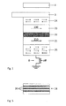
- Fig. 1 shows a MRAM element 1 comprising a magnetic tunnel junction 2 according to an embodiment.
- the magnetic tunnel junction 2 comprises a reference layer 21 having a fixed reference magnetization 210, a storage layer 23 having a storage magnetization 230, and a tunnel barrier layer 22 comprised between the sense and the storage layers 21, 23.
- the tunnel barrier layer 22 is a thin layer, typically in the nanometer range and can be formed, for example, from any suitable insulating material, such as alumina or magnesium oxide.
- the tunnel barrier layer 22 has an electrical resistivity comprised between about 1 m ⁇ -cm and 3000 m ⁇ -cm.
- the magnetic tunnel junction 2 further comprises a storage antiferromagnetic layer exchange-coupling the storage layer 23 such as to pin the storage magnetization 230 when the magnetic tunnel junction 2 is at a low temperature threshold, below a critical temperature of the antiferromagnetic layer 24 and free the storage magnetization 230 when the magnetic tunnel junction 2 is heated at a high temperature threshold, at and above the critical temperature.
- the storage antiferromagnetic layer 24 further has an electrical resistivity that is the same order of magnitude than the electrical resistivity of tunnel barrier layer 22.
- the storage antiferromagnetic layer 24 has an electrical resistivity that is comprised between about 1 m ⁇ -cm and 3000 m ⁇ -cm.
- Such storage antiferromagnetic layer 24 is thus further adapted for heating the magnetic tunnel junction 2 when the heating current 31 is passed in the magnetic tunnel junction 2 via the current line 3.
- the storage antiferromagnetic layer 24 comprises an oxide such as a CoO-based oxide or a NiO-based oxide or an oxide comprising Co and/or Ni.
- the oxide comprises CoNiO.
- the CoNiO -based storage antiferromagnetic layer 24 advantageously combines the high magnetocrystalline anisotropy of the CoO and the high blocking temperature of the NiO.
- the oxide storage antiferromagnetic layer 24 allows for obtaining the electrical resistivity being comprised between about 1 m ⁇ -cm and 3000 m ⁇ -cm.
- the electrical resistivity of the storage antiferromagnetic layer 24 can be further adjusted by adding at least one metallic element to the storage antiferromagnetic layer 24.
- the added metallic element can comprise at least one of copper, tantalum or ruthenium.
- the added metallic element comprises one or a plurality of metallic layers 26 included (for example inserted) in the storage antiferromagnetic layer 24.
- Fig. 5 represents the storage antiferromagnetic layer 24 in isolation from the rest of the magnetic tunnel junction 2 and comprising the metallic layers 26.
- Each metallic layer 26 can have a thickness smaller than 0.5 nm.
- Each metallic layer 26 can further comprise at least one of copper, tantalum or ruthenium.
- the one or plurality of metallic elements can be comprised in the storage antiferromagnetic layer 24 in any other ways including in the form of islands of the metallic element within the antiferromagnetic material or mixed homogeneously with the antiferromagnetic material.
- the magnetic tunnel junction 2 can further comprise a reference antiferromagnetic layer 25 exchange-coupling the reference layer 21.
- the reference antiferromagnetic layer 24 can comprise PtMn, IrMn, or any other suitable materials such as to pin the reference magnetization 210 when the magnetic tunnel junction 2 is at the low and high temperature threshold.
- the MRAM element 1 further comprises a current line 3 in electrical contact with one end of the magnetic tunnel junction 2.
- the current line 3 is adapted for passing a heating current 31 in the magnetic tunnel junction 2 via the current line 3 for heating the magnetic tunnel junction 2.
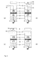
- FIG. 2a to 2d A method for writing the MRAM element 1 is illustrated in Figs. 2a to 2d , according to an embodiment and comprising the steps of:
- the MRAM element 1 comprises a select transistor 8 electrically connected to the other end of the magnetic tunnel junction 2.
- the select transistor 8 can be put in a passing mode (ON) allowing the heating current 31 to pass in the magnetic tunnel junction 2.
- Fig. 2b represents switching the storage magnetization 230 by applying a write magnetic field 42. More particularly, the write magnetic field 42 is generated by passing a field current 41 in a field line 4 represented on top of the current line 4 in the examples of Figs 2a to 2d. Other arrangements are also possible. For example, the field line 4 can be placed at the other end of the magnetic tunnel junction 2. Alternatively, the filed current 41 can be passed in the current line 3, avoiding the extra field line 4. As shown in Figs. 2a and 2b , the storage magnetization 230 is switched form an initial orientation substantially parallel to the reference magnetization 210 ( Fig. 2a ) to a switched orientation substantially antiparallel to the reference magnetization 210 ( Fig. 2b ).
- the heating current 31 is then turned off, for example by setting the select transistor 8 in a closed mode (OFF), such as to cool down the magnetic tunnel junction 2 below the critical temperature.
- the write magnetic field can be applied as represented in Fig. 2c .
- the write magnetic field 42 can be removed ( Fig. 2d ).
- the storage antiferromagnetic layer 24, having an electrical resistivity being on the same order of magnitude as the one of the tunnel barrier layer 22 will thus function as a heating element when the heating current 31 is passed in the magnetic tunnel junction 2.
- An advantage of the storage antiferromagnetic layer 24 functioning as heating element is that the heating is local, i.e., is produced in the vicinity of the storage layer 23. This results in improved heating efficacy and improved reliability of the MRAM element 1 as the voltage due to the passage of the heating current 31 is shared between the tunnel barrier layer 22 and the antiferromagnetic oxide layer 24.
- the storage antiferromagnetic layer 24 further provides the exchange-coupling between the storage antiferromagnetic layer 24 and the storage layer 23 as disclosed above.
- the resistance R across the MRAM element 1, and thus data state, is determined by the orientation of the storage magnetization 230 relative to the reference magnetization 210.
- the reference magnetization 210 is pinned in a predetermined direction while the direction of the storage magnetization 230 can be switched as described above.
- a read current 32 can be passed in the magnetic tunnel junction 2 via the current line 3 such as to measure the resistance R across the MRAM element 1.
- a low resistance value (data state "0") is measured when the storage magnetization 230 is substantially parallel to the reference magnetization 210.
- a high resistance value (data state "1") is measured when the storage magnetization 230 is substantially antiparallel to the reference magnetization 210.
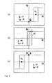
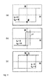
- Figs. 3 and 4 show hysteresis loops, or magnetization curves, for the MRAM element 1 in the respective configurations of Fig. 1 , 2b and 2d , wherein change in the resistance R of the MRAM element 1 is plotted as a function of the magnetic field H.
- Fig. 3 (a) to (c) correspond to the case where the exchange-coupling between the storage layer 23 and the storage antiferromagnetic layer 24 provides an exchange bias H B causing a shift in the magnetization curve of the storage layer 23 in proportion with the exchange bias H B .
- Fig. 3(a) illustrates the case where the storage magnetization 230 is parallel to the reference magnetization (see Fig. 2(a) ) and the magnetization curve of the storage layer 23 is shifted in proportion with the exchange bias H B , towards positive magnetic field values (towards the right on figure 3(a) ). In the absence of the write magnetic field 42, the MRAM element 1 is in the data state "0".
- the magnetization curve is symmetric and centred around a null magnetic field ( Fig. 3(b) ).
- the write magnetic field 42 (represented by the dashed line) is applied with a magnitude corresponding to the saturation of the storage magnetization 230 such that the storage magnetization 230 can be switched from its initial orientation parallel to the reference magnetization 210 to a switched orientation antiparallel to the reference magnetization 210.
- the magnetization curve with the storage magnetization 230 in the switched orientation is shown in Fig. 3(c) being shifted towards negative magnetic field values (towards the left on figure 3(c) ) in proportion with the exchange bias H B yielding data state "0" in the absence of the write magnetic field 42.
- the magnetization curves in the Figs. 3 (a) to (c) correspond to the case where the storage antiferromagnetic layer 24 comprises relatively large grain sizes typically larger than 10 nm or/and where the storage layer 23 and the storage antiferromagnetic layer 24 have been grown in a magnetic field or after growth is annealed in a magnetic field to temperatures above Néel temperature of the storage antiferromagnetic layer 24.
- the exchange bias H B reflects the fact that there is a preferred easy magnetization direction for the storage layer 23; the storage magnetization 230 being pinned by the storage antiferromagnetic layer 24 into this direction.
- magnetization curves shown in Figs. 4(a) to (c) correspond to the case where the exchange-coupling between the storage layer 23 and the storage antiferromagnetic layer 24 increases the coercivity of the storage layer 23 at the low temperature threshold.
- the increased coercivity is larger than the exchange bias field H B .
- the storage antiferromagnetic layer 24 comprises relatively small grain sizes typically smaller than 10 nm.
- the exchange-coupling between the two layers 23, 24 only leads to an increased coercivity of the storage layer 23 as shown in in Fig.
- the magnetic tunnel junction 2 is heated at the high temperature threshold by passing the heating current 31 where the exchange-coupling between the storage antiferromagnetic layer 24 and the storage layer 23 vanishes.
- the magnetization curve shows smaller coercivity of the unpinned storage layer 23 such that the write magnetic field 42 can be applied with a small magnitude to switch the storage magnetization from its initial orientation parallel to the reference magnetization 210 to the switched orientation antiparallel to the reference magnetization 210.
- the storage layer 23 is again exchange-coupled by the storage antiferromagnetic layer 24, increasing the coercivity of the storage layer 23.
- the magnetization curve remains symmetric ( Fig. 4(c) ).
Landscapes
- Engineering & Computer Science (AREA)
- Computer Hardware Design (AREA)
- Mram Or Spin Memory Techniques (AREA)
- Hall/Mr Elements (AREA)
Abstract
Description
- The present disclosure concerns a thermally assisted switching magnetic random access memory (MRAM) element having better data retention and low writing mode operating temperature.
- Thermally-assisted MRAM elements are known. A MRAM element typically comprises a magnetic tunnel junction including a reference layer having a reference magnetization; a storage layer having a storage magnetization; a tunnel barrier layer included between the storage layer and the reference layer; and a storage antiferromagnetic layer exchange-coupling the storage layer such as to pin the storage magnetization at a low temperature threshold and to free it at a high temperature threshold. Pinning of the storage magnetization is usually due to an exchange bias provided by the exchange-coupling at the low temperature threshold.
- For small MRAM element, typically its size is decreased below 100nm, the exchange bias provided by the storage antiferromagnetic layer at the low temperature threshold can become instable. The instability is related to grain size distributions of the antiferromagnetic layer, characteristic of manganese based alloys comprised in the antiferromagnetic layer.
- Moreover, reliability of the MRAM element can be further impaired when such MRAM element is used in high temperature applications. Indeed, the heating voltage needed to free the storage magnetization can get close to the breakdown voltage of the magnetic tunnel junction.
- The present disclosure concerns a MRAM element having a magnetic tunnel junction comprising: a reference layer having a fixed reference magnetization; a storage layer having a storage magnetization; a tunnel barrier layer between the storage layer and the reference layer; and a storage antiferromagnetic layer; the MRAM element further comprising a current line in electrical contact with one end of the magnetic tunnel junction and arranged for passing a heating current in the magnetic tunnel junction for heating the magnetic tunnel junction; wherein the storage antiferromagnetic layer having a first function of pinning the storage magnetization when the magnetic tunnel junction is at a low threshold temperature and freeing the storage magnetization when the magnetic tunnel junction is heated at a high threshold temperature; and wherein the storage antiferromagnetic layer further having an electrical resistivity comprised between about 1 mΩ-cm and 3000 mΩ-cm such that the storage antiferromagnetic layer has a second function of heating the magnetic tunnel junction when the heating current is passed in the magnetic tunnel junction via the current line.
- In an embodiment, the storage antiferromagnetic layer comprises an oxide. The oxide can comprise a CoO oxide or a NiO oxide or an oxide comprising Co and/or Ni. The oxide can further comprise a CoNiO oxide.
- In another embodiment, the storage antiferromagnetic layer can further comprise at least one metallic element such as to vary the electrical resistivity of the storage antiferromagnetic layer. The metallic element can comprise at least one of copper, tantalum or ruthenium.
- In yet another embodiment, pinning and freeing of the storage magnetization can be obtained via exchange bias between the storage antiferromagnetic layer and the storage layer, or by increased coercivity of the storage layer by the storage antiferromagnetic layer.
- The present disclosure further pertains to a method for writing the MRAM element. comprising:
- heating the magnetic tunnel junction at or above the critical temperature;
- once the storage antiferromagnetic layer has reached the critical temperature, switching the storage magnetization in a written state;
- cooling the magnetic tunnel junction to a temperature being below the critical temperature such as to pin the storage magnetization in the written state.
- The disclosed MRAM element has better data retention and low writing temperature.
- The disclosure will be better understood with the aid of the description of an embodiment given by way of example and illustrated by the figures, in which:
-
Fig. 1 shows a view a MRAM element according to an embodiment; -
Figs. 2(a) to (d) illustrate a method for writing the MRAM element, according to an embodiment; -
Figs. 3(a) to (c) show magnetization curves for the MRAM element, according to an embodiment; -
Figs. 4(a) to (c) show magnetization curves for the MRAM element, according to another embodiment; and -
Fig. 5 represents a storage antiferromagnetic layer of the MRAM element, according to an embodiment. -
Fig. 1 shows a MRAM element 1 comprising a magnetic tunnel junction 2 according to an embodiment. The magnetic tunnel junction 2 comprises areference layer 21 having afixed reference magnetization 210, astorage layer 23 having astorage magnetization 230, and atunnel barrier layer 22 comprised between the sense and thestorage layers tunnel barrier layer 22 is a thin layer, typically in the nanometer range and can be formed, for example, from any suitable insulating material, such as alumina or magnesium oxide. Typically, thetunnel barrier layer 22 has an electrical resistivity comprised between about 1 mΩ-cm and 3000 mΩ-cm. - The magnetic tunnel junction 2 further comprises a storage antiferromagnetic layer exchange-coupling the
storage layer 23 such as to pin thestorage magnetization 230 when the magnetic tunnel junction 2 is at a low temperature threshold, below a critical temperature of theantiferromagnetic layer 24 and free thestorage magnetization 230 when the magnetic tunnel junction 2 is heated at a high temperature threshold, at and above the critical temperature. - The storage
antiferromagnetic layer 24 further has an electrical resistivity that is the same order of magnitude than the electrical resistivity oftunnel barrier layer 22. For example, the storageantiferromagnetic layer 24 has an electrical resistivity that is comprised between about 1 mΩ-cm and 3000 mΩ-cm. Such storageantiferromagnetic layer 24 is thus further adapted for heating the magnetic tunnel junction 2 when theheating current 31 is passed in the magnetic tunnel junction 2 via thecurrent line 3. - In an embodiment, the storage
antiferromagnetic layer 24 comprises an oxide such as a CoO-based oxide or a NiO-based oxide or an oxide comprising Co and/or Ni. In a preferred embodiment, the oxide comprises CoNiO. The CoNiO -based storageantiferromagnetic layer 24 advantageously combines the high magnetocrystalline anisotropy of the CoO and the high blocking temperature of the NiO. The oxide storageantiferromagnetic layer 24 allows for obtaining the electrical resistivity being comprised between about 1 mΩ-cm and 3000 mΩ-cm. The electrical resistivity of the storageantiferromagnetic layer 24 can be further adjusted by adding at least one metallic element to the storageantiferromagnetic layer 24. Preferably, the added metallic element can comprise at least one of copper, tantalum or ruthenium. In an embodiment, the added metallic element comprises one or a plurality ofmetallic layers 26 included (for example inserted) in the storageantiferromagnetic layer 24.Fig. 5 represents the storageantiferromagnetic layer 24 in isolation from the rest of the magnetic tunnel junction 2 and comprising themetallic layers 26. Eachmetallic layer 26 can have a thickness smaller than 0.5 nm. Eachmetallic layer 26 can further comprise at least one of copper, tantalum or ruthenium. The one or plurality of metallic elements can be comprised in the storageantiferromagnetic layer 24 in any other ways including in the form of islands of the metallic element within the antiferromagnetic material or mixed homogeneously with the antiferromagnetic material. - The magnetic tunnel junction 2 can further comprise a reference
antiferromagnetic layer 25 exchange-coupling thereference layer 21. The referenceantiferromagnetic layer 24 can comprise PtMn, IrMn, or any other suitable materials such as to pin thereference magnetization 210 when the magnetic tunnel junction 2 is at the low and high temperature threshold. - The MRAM element 1 further comprises a
current line 3 in electrical contact with one end of the magnetic tunnel junction 2. Thecurrent line 3 is adapted for passing aheating current 31 in the magnetic tunnel junction 2 via thecurrent line 3 for heating the magnetic tunnel junction 2. - A method for writing the MRAM element 1 is illustrated in
Figs. 2a to 2d , according to an embodiment and comprising the steps of: - heating the magnetic tunnel junction 2 at or above the critical temperature;
- once the storage
antiferromagnetic layer 24 has reached the critical temperature, switching thestorage magnetization 230 in a written state; - cooling the magnetic tunnel junction 2 to a temperature being below the critical temperature such as to pin the
storage magnetization 230 in the written state. - In particular, heating the magnetic tunnel junction 2 by passing the
heating current 31 in the magnetic tunnel junction 2 via thecurrent line 3 is shown inFig. 2a . As shown in the figure, the MRAM element 1 comprises aselect transistor 8 electrically connected to the other end of the magnetic tunnel junction 2. Theselect transistor 8 can be put in a passing mode (ON) allowing theheating current 31 to pass in the magnetic tunnel junction 2. -
Fig. 2b represents switching thestorage magnetization 230 by applying a writemagnetic field 42. More particularly, the writemagnetic field 42 is generated by passing a field current 41 in afield line 4 represented on top of thecurrent line 4 in the examples ofFigs 2a to 2d. Other arrangements are also possible. For example, thefield line 4 can be placed at the other end of the magnetic tunnel junction 2. Alternatively, the filed current 41 can be passed in thecurrent line 3, avoiding theextra field line 4. As shown inFigs. 2a and 2b , thestorage magnetization 230 is switched form an initial orientation substantially parallel to the reference magnetization 210 (Fig. 2a ) to a switched orientation substantially antiparallel to the reference magnetization 210 (Fig. 2b ). - The heating current 31 is then turned off, for example by setting the
select transistor 8 in a closed mode (OFF), such as to cool down the magnetic tunnel junction 2 below the critical temperature. During the cooling step, the write magnetic field can be applied as represented inFig. 2c . Once the magnetic tunnel junction is below the critical temperature such that thestorage magnetization 230 is pinned in the written state, the writemagnetic field 42 can be removed (Fig. 2d ). - During the writing of the MRAM element 1, the storage
antiferromagnetic layer 24, having an electrical resistivity being on the same order of magnitude as the one of thetunnel barrier layer 22 will thus function as a heating element when the heating current 31 is passed in the magnetic tunnel junction 2. An advantage of the storageantiferromagnetic layer 24 functioning as heating element is that the heating is local, i.e., is produced in the vicinity of thestorage layer 23. This results in improved heating efficacy and improved reliability of the MRAM element 1 as the voltage due to the passage of the heating current 31 is shared between thetunnel barrier layer 22 and theantiferromagnetic oxide layer 24. - During the writing of the MRAM element 1, the storage
antiferromagnetic layer 24 further provides the exchange-coupling between the storageantiferromagnetic layer 24 and thestorage layer 23 as disclosed above. - The resistance R across the MRAM element 1, and thus data state, is determined by the orientation of the
storage magnetization 230 relative to thereference magnetization 210. Thereference magnetization 210 is pinned in a predetermined direction while the direction of thestorage magnetization 230 can be switched as described above. - During a read operation, a read current 32 can be passed in the magnetic tunnel junction 2 via the
current line 3 such as to measure the resistance R across the MRAM element 1. A low resistance value (data state "0") is measured when thestorage magnetization 230 is substantially parallel to thereference magnetization 210. Conversely, a high resistance value (data state "1") is measured when thestorage magnetization 230 is substantially antiparallel to thereference magnetization 210. -
Figs. 3 and4 show hysteresis loops, or magnetization curves, for the MRAM element 1 in the respective configurations ofFig. 1 ,2b and 2d , wherein change in the resistance R of the MRAM element 1 is plotted as a function of the magnetic field H. - In particular,
Fig. 3 (a) to (c) correspond to the case where the exchange-coupling between thestorage layer 23 and the storageantiferromagnetic layer 24 provides an exchange bias HB causing a shift in the magnetization curve of thestorage layer 23 in proportion with the exchange bias HB.Fig. 3(a) illustrates the case where thestorage magnetization 230 is parallel to the reference magnetization (seeFig. 2(a) ) and the magnetization curve of thestorage layer 23 is shifted in proportion with the exchange bias HB, towards positive magnetic field values (towards the right onfigure 3(a) ). In the absence of the writemagnetic field 42, the MRAM element 1 is in the data state "0". - When the magnetic tunnel junction 2 is heated at the high temperature threshold by passing the heating current 31 (
Fig. 2(b) ), the exchange coupling vanishes and there is no more exchange bias HB. The magnetization curve is symmetric and centred around a null magnetic field (Fig. 3(b) ). The write magnetic field 42 (represented by the dashed line) is applied with a magnitude corresponding to the saturation of thestorage magnetization 230 such that thestorage magnetization 230 can be switched from its initial orientation parallel to thereference magnetization 210 to a switched orientation antiparallel to thereference magnetization 210. The magnetization curve with thestorage magnetization 230 in the switched orientation is shown inFig. 3(c) being shifted towards negative magnetic field values (towards the left onfigure 3(c) ) in proportion with the exchange bias HB yielding data state "0" in the absence of the writemagnetic field 42. - The magnetization curves in the
Figs. 3 (a) to (c) correspond to the case where the storageantiferromagnetic layer 24 comprises relatively large grain sizes typically larger than 10 nm or/and where thestorage layer 23 and the storageantiferromagnetic layer 24 have been grown in a magnetic field or after growth is annealed in a magnetic field to temperatures above Néel temperature of the storageantiferromagnetic layer 24. The exchange bias HB reflects the fact that there is a preferred easy magnetization direction for thestorage layer 23; thestorage magnetization 230 being pinned by the storageantiferromagnetic layer 24 into this direction. - In contrast, magnetization curves shown in
Figs. 4(a) to (c) correspond to the case where the exchange-coupling between thestorage layer 23 and the storageantiferromagnetic layer 24 increases the coercivity of thestorage layer 23 at the low temperature threshold. Here, the increased coercivity is larger than the exchange bias field HB. This case happens when the storageantiferromagnetic layer 24 comprises relatively small grain sizes typically smaller than 10 nm. Furthermore, whenstorage layer 23 is simply grown on top of the storageantiferromagnetic layer 24 the exchange-coupling between the twolayers storage layer 23 as shown in inFig. 4(a) representing the initial data state "0" wherein thestorage magnetization 230 is oriented parallel to thereference magnetization 210. This is usually attributed to the increased coercivity of "interfacial spins" which exchange bias need to be dragged around by the writemagnetic field 42. However, the magnetization curve is still symmetric, indicating two equivalent easy directions. - In
Fig. 4(b) , the magnetic tunnel junction 2 is heated at the high temperature threshold by passing the heating current 31 where the exchange-coupling between the storageantiferromagnetic layer 24 and thestorage layer 23 vanishes. The magnetization curve shows smaller coercivity of theunpinned storage layer 23 such that the writemagnetic field 42 can be applied with a small magnitude to switch the storage magnetization from its initial orientation parallel to thereference magnetization 210 to the switched orientation antiparallel to thereference magnetization 210. Once the magnetic tunnel junction 2 has been cooled down to the low temperature threshold thestorage layer 23 is again exchange-coupled by the storageantiferromagnetic layer 24, increasing the coercivity of thestorage layer 23. The magnetization curve remains symmetric (Fig. 4(c) ).Reference numbers and symbols 1 MRAM element 2 magnetic tunnel junction 21 reference layer 210 reference magnetization 22 tunnel barrier layer 23 storage layer 230 storage magnetization 24 storage antiferromagnetic layer 25 reference antiferromagnetic layer 26 layer of metallic element 41 field current 42 write magnetic field 8 select transistor H magnetic field HB exchange bias R resistance of the MRAM element
Claims (14)
- MRAM element (1) having a magnetic tunnel junction (2) comprising:a reference layer (21) having a fixed reference magnetization (210);a storage layer (23) having a storage magnetization (230);a tunnel barrier layer (22) between the storage layer (23) and the reference layer (21); anda storage antiferromagnetic layer (24);the MRAM element (1) further comprising a current line (3) in electrical contact with one end of the magnetic tunnel junction (2) and arranged for passing a heating current (31) in the magnetic tunnel junction (2) for heating the magnetic tunnel junction (2); whereinthe storage antiferromagnetic layer (24) having a first function of pinning the storage magnetization (230) when the magnetic tunnel junction (2) is at a low threshold temperature and freeing the storage magnetization (230) when the magnetic tunnel junction (2) is heated at a high threshold temperature; and whereinthe storage antiferromagnetic layer (24) further having an electrical resistivity comprised between about 1 mΩ-cm and 3000 mΩ-cm such that the storage antiferromagnetic layer (24) has a second function of heating the magnetic tunnel junction (2) when the heating current is passed in the magnetic tunnel junction (2) via the current line (3).
- The MRAM element (1) according to claim 1, wherein the storage antiferromagnetic layer (24) comprises an oxide.
- The MRAM element (1) according to claim 2, wherein the oxide comprises a CoO oxide or a NiO oxide or an oxide comprising Co and/or Ni.
- The MRAM element (1) according to claim 3, wherein the oxide comprises a CoNiO oxide.
- The MRAM element (1) according to any one of claims 1 to 4, wherein
the storage antiferromagnetic layer (24) further comprises at least one metallic element such as to vary the electrical resistivity of the storage antiferromagnetic layer (24). - The MRAM element (1) according to claim 5, wherein said at least one metallic element comprises at least one of copper, tantalum or ruthenium.
- The MRAM element (1) according to claim 5, wherein said at least one metallic element comprises one or a plurality of metallic layers (26) included in the storage antiferromagnetic layer (24).
- The MRAM element (1) according to claim 7, wherein each of said one or a plurality of metallic layers (26) has a thicknesses smaller than 0.5 nm.
- The MRAM element (1) according to claim 7 or 8, wherein each of said one or a plurality of metallic layers (26) further comprises at least one of copper, tantalum or ruthenium.
- The MRAM element (1) according to any one of claims 1 to 6, wherein
the storage antiferromagnetic layer (24) is arranged such that said pinning and freeing of the storage magnetization (230) is obtained via exchange bias (HB) between the storage antiferromagnetic layer (24) and the storage layer (23). - The MRAM element (1) according to claim 7, wherein the storage antiferromagnetic layer (24) has grain size above 10 nm.
- The MRAM element (1) according to any one of claims 1 to 6, wherein
the storage antiferromagnetic layer (24) is arranged such that said pinning and freeing of the storage magnetization (230) is obtained via increased coercivity of the storage layer (23) by the storage antiferromagnetic layer (24). - The MRAM element (1) according to claim 9, wherein the storage antiferromagnetic layer (24) has grain size below 10 nm.
- A method for writing the MRAM element (1) according to any one of claims 1 to 10, comprising:heating the magnetic tunnel junction (2) at or above the critical temperature;once the storage antiferromagnetic layer (24) has reached the critical temperature, switching the storage magnetization (230) in a written state;cooling the magnetic tunnel junction (2) to a temperature being below the critical temperature such as to pin the storage magnetization (230) in the written state.
Priority Applications (3)
| Application Number | Priority Date | Filing Date | Title |
|---|---|---|---|
| EP13290019.2A EP2760025B1 (en) | 2013-01-23 | 2013-01-23 | TAS-MRAM element with low writing temperature |
| US14/762,264 US9336846B2 (en) | 2013-01-23 | 2014-01-16 | MRAM element with low writing temperature |
| PCT/EP2014/050772 WO2014114550A1 (en) | 2013-01-23 | 2014-01-16 | Mram element with low writing temperature |
Applications Claiming Priority (1)
| Application Number | Priority Date | Filing Date | Title |
|---|---|---|---|
| EP13290019.2A EP2760025B1 (en) | 2013-01-23 | 2013-01-23 | TAS-MRAM element with low writing temperature |
Publications (2)
| Publication Number | Publication Date |
|---|---|
| EP2760025A1 true EP2760025A1 (en) | 2014-07-30 |
| EP2760025B1 EP2760025B1 (en) | 2019-01-02 |
Family
ID=48537909
Family Applications (1)
| Application Number | Title | Priority Date | Filing Date |
|---|---|---|---|
| EP13290019.2A Active EP2760025B1 (en) | 2013-01-23 | 2013-01-23 | TAS-MRAM element with low writing temperature |
Country Status (3)
| Country | Link |
|---|---|
| US (1) | US9336846B2 (en) |
| EP (1) | EP2760025B1 (en) |
| WO (1) | WO2014114550A1 (en) |
Cited By (1)
| Publication number | Priority date | Publication date | Assignee | Title |
|---|---|---|---|---|
| US11894029B1 (en) * | 2022-10-27 | 2024-02-06 | Globalfoundries Singapore Pte. Ltd. | Spiking neural network hardware based on magnetic-tunnel-junction layer stacks |
Families Citing this family (1)
| Publication number | Priority date | Publication date | Assignee | Title |
|---|---|---|---|---|
| CN112259139B (en) * | 2019-07-22 | 2022-09-30 | 中电海康集团有限公司 | Memory cell, memory, and method for initializing memory |
Citations (4)
| Publication number | Priority date | Publication date | Assignee | Title |
|---|---|---|---|---|
| WO2003043017A2 (en) * | 2001-11-16 | 2003-05-22 | Commissariat A L'energie Atomique | Magnetic device with magnetic tunnel junction, memory array and read/write methods using same |
| US6819586B1 (en) * | 2003-10-24 | 2004-11-16 | Hewlett-Packard Development Company, L.P. | Thermally-assisted magnetic memory structures |
| US20070189064A1 (en) * | 2006-02-14 | 2007-08-16 | Magic Technologies, Inc. | Multi-state thermally assisted storage |
| US20120119313A1 (en) * | 2010-11-16 | 2012-05-17 | Seagate Technology Llc | Memory Cell With Phonon-Blocking Insulating Layer |
Family Cites Families (3)
| Publication number | Priority date | Publication date | Assignee | Title |
|---|---|---|---|---|
| JP5095076B2 (en) * | 2004-11-09 | 2012-12-12 | 株式会社東芝 | Magnetoresistive effect element |
| US7643332B2 (en) * | 2006-06-23 | 2010-01-05 | Infineon Technologies Ag | MRAM cell using multiple axes magnetization and method of operation |
| EP2528060B1 (en) * | 2011-05-23 | 2016-12-14 | Crocus Technology S.A. | Multibit cell with synthetic storage layer |
-
2013
- 2013-01-23 EP EP13290019.2A patent/EP2760025B1/en active Active
-
2014
- 2014-01-16 US US14/762,264 patent/US9336846B2/en active Active
- 2014-01-16 WO PCT/EP2014/050772 patent/WO2014114550A1/en not_active Ceased
Patent Citations (4)
| Publication number | Priority date | Publication date | Assignee | Title |
|---|---|---|---|---|
| WO2003043017A2 (en) * | 2001-11-16 | 2003-05-22 | Commissariat A L'energie Atomique | Magnetic device with magnetic tunnel junction, memory array and read/write methods using same |
| US6819586B1 (en) * | 2003-10-24 | 2004-11-16 | Hewlett-Packard Development Company, L.P. | Thermally-assisted magnetic memory structures |
| US20070189064A1 (en) * | 2006-02-14 | 2007-08-16 | Magic Technologies, Inc. | Multi-state thermally assisted storage |
| US20120119313A1 (en) * | 2010-11-16 | 2012-05-17 | Seagate Technology Llc | Memory Cell With Phonon-Blocking Insulating Layer |
Non-Patent Citations (1)
| Title |
|---|
| LANG X Y ET AL: "Dependence of the blocking temperature in exchange biased ferromagnetic/antiferromagnetic bilayers on the thickness of the antiferromagnetic layer", NANOTECHNOLOGY, IOP, BRISTOL, GB, vol. 18, no. 15, 18 April 2007 (2007-04-18), pages 155701, XP020119025, ISSN: 0957-4484, DOI: 10.1088/0957-4484/18/15/155701 * |
Cited By (1)
| Publication number | Priority date | Publication date | Assignee | Title |
|---|---|---|---|---|
| US11894029B1 (en) * | 2022-10-27 | 2024-02-06 | Globalfoundries Singapore Pte. Ltd. | Spiking neural network hardware based on magnetic-tunnel-junction layer stacks |
Also Published As
| Publication number | Publication date |
|---|---|
| EP2760025B1 (en) | 2019-01-02 |
| US9336846B2 (en) | 2016-05-10 |
| US20150357014A1 (en) | 2015-12-10 |
| WO2014114550A1 (en) | 2014-07-31 |
Similar Documents
| Publication | Publication Date | Title |
|---|---|---|
| JP6200471B2 (en) | Magnetic memory | |
| KR101706613B1 (en) | Perpendicular mtj stacks including magnetic anisotropy enhancing layer and crystallization barrier layer | |
| EP2249350B1 (en) | Magnetic memory with a thermally assisted spin transfer torque writing procedure using a low writing current | |
| US10953319B2 (en) | Spin transfer MRAM element having a voltage bias control | |
| US9287493B2 (en) | Storage element and memory | |
| US7796428B2 (en) | Thermally assisted magnetic write memory | |
| JP4496189B2 (en) | Magnetoresistive element and magnetoresistive random access memory | |
| US9680088B2 (en) | Ferromagnetic tunnel junction element and method of driving ferromagnetic tunnel junction element | |
| RU2599948C2 (en) | Self-referenced magnetic random access memory element comprising synthetic storage layer | |
| US20130037862A1 (en) | Magnetic random access memory | |
| TWI639155B (en) | Storage element, storage device, and magnetic head | |
| US8625327B2 (en) | Magnetic random access memory and initializing method for the same | |
| TWI482152B (en) | Memory device, memory device | |
| JP6126565B2 (en) | Magnetoresistive element and magnetic memory | |
| KR102412195B1 (en) | Magnetic junction, magnetic memory and method for providing magnetic junction | |
| US8503225B2 (en) | Multibit cell with synthetic storage layer | |
| US20160005449A1 (en) | Method and system for providing magnetic junctions with rare earth-transition metal layers | |
| US20100103565A1 (en) | St-ram employing heusler alloys | |
| JP2007048790A (en) | Memory element and memory | |
| EP2775480A1 (en) | Self-referenced TAS-MRAM cell that can be read with reduced power consumption | |
| US9336846B2 (en) | MRAM element with low writing temperature | |
| JP2013048124A (en) | Ferromagnetic tunnel junction element | |
| JP2008004625A (en) | Memory element and memory | |
| JP2014033076A (en) | Magnetoresistance effect element |
Legal Events
| Date | Code | Title | Description |
|---|---|---|---|
| PUAI | Public reference made under article 153(3) epc to a published international application that has entered the european phase |
Free format text: ORIGINAL CODE: 0009012 |
|
| 17P | Request for examination filed |
Effective date: 20130123 |
|
| AK | Designated contracting states |
Kind code of ref document: A1 Designated state(s): AL AT BE BG CH CY CZ DE DK EE ES FI FR GB GR HR HU IE IS IT LI LT LU LV MC MK MT NL NO PL PT RO RS SE SI SK SM TR |
|
| AX | Request for extension of the european patent |
Extension state: BA ME |
|
| R17P | Request for examination filed (corrected) |
Effective date: 20141216 |
|
| RBV | Designated contracting states (corrected) |
Designated state(s): AL AT BE BG CH CY CZ DE DK EE ES FI FR GB GR HR HU IE IS IT LI LT LU LV MC MK MT NL NO PL PT RO RS SE SI SK SM TR |
|
| STAA | Information on the status of an ep patent application or granted ep patent |
Free format text: STATUS: EXAMINATION IS IN PROGRESS |
|
| 17Q | First examination report despatched |
Effective date: 20161104 |
|
| GRAP | Despatch of communication of intention to grant a patent |
Free format text: ORIGINAL CODE: EPIDOSNIGR1 |
|
| STAA | Information on the status of an ep patent application or granted ep patent |
Free format text: STATUS: GRANT OF PATENT IS INTENDED |
|
| RIC1 | Information provided on ipc code assigned before grant |
Ipc: H01L 43/02 20060101ALI20180709BHEP Ipc: G11C 11/16 20060101AFI20180709BHEP Ipc: H01L 43/10 20060101ALI20180709BHEP Ipc: H01L 43/08 20060101ALI20180709BHEP |
|
| INTG | Intention to grant announced |
Effective date: 20180726 |
|
| GRAS | Grant fee paid |
Free format text: ORIGINAL CODE: EPIDOSNIGR3 |
|
| GRAA | (expected) grant |
Free format text: ORIGINAL CODE: 0009210 |
|
| STAA | Information on the status of an ep patent application or granted ep patent |
Free format text: STATUS: THE PATENT HAS BEEN GRANTED |
|
| AK | Designated contracting states |
Kind code of ref document: B1 Designated state(s): AL AT BE BG CH CY CZ DE DK EE ES FI FR GB GR HR HU IE IS IT LI LT LU LV MC MK MT NL NO PL PT RO RS SE SI SK SM TR |
|
| REG | Reference to a national code |
Ref country code: GB Ref legal event code: FG4D |
|
| REG | Reference to a national code |
Ref country code: CH Ref legal event code: EP Ref country code: AT Ref legal event code: REF Ref document number: 1085395 Country of ref document: AT Kind code of ref document: T Effective date: 20190115 |
|
| REG | Reference to a national code |
Ref country code: IE Ref legal event code: FG4D |
|
| REG | Reference to a national code |
Ref country code: DE Ref legal event code: R096 Ref document number: 602013049121 Country of ref document: DE |
|
| REG | Reference to a national code |
Ref country code: NL Ref legal event code: MP Effective date: 20190102 |
|
| REG | Reference to a national code |
Ref country code: LT Ref legal event code: MG4D |
|
| REG | Reference to a national code |
Ref country code: AT Ref legal event code: MK05 Ref document number: 1085395 Country of ref document: AT Kind code of ref document: T Effective date: 20190102 |
|
| PG25 | Lapsed in a contracting state [announced via postgrant information from national office to epo] |
Ref country code: NL Free format text: LAPSE BECAUSE OF FAILURE TO SUBMIT A TRANSLATION OF THE DESCRIPTION OR TO PAY THE FEE WITHIN THE PRESCRIBED TIME-LIMIT Effective date: 20190102 |
|
| PG25 | Lapsed in a contracting state [announced via postgrant information from national office to epo] |
Ref country code: NO Free format text: LAPSE BECAUSE OF FAILURE TO SUBMIT A TRANSLATION OF THE DESCRIPTION OR TO PAY THE FEE WITHIN THE PRESCRIBED TIME-LIMIT Effective date: 20190402 Ref country code: PL Free format text: LAPSE BECAUSE OF FAILURE TO SUBMIT A TRANSLATION OF THE DESCRIPTION OR TO PAY THE FEE WITHIN THE PRESCRIBED TIME-LIMIT Effective date: 20190102 Ref country code: SE Free format text: LAPSE BECAUSE OF FAILURE TO SUBMIT A TRANSLATION OF THE DESCRIPTION OR TO PAY THE FEE WITHIN THE PRESCRIBED TIME-LIMIT Effective date: 20190102 Ref country code: FI Free format text: LAPSE BECAUSE OF FAILURE TO SUBMIT A TRANSLATION OF THE DESCRIPTION OR TO PAY THE FEE WITHIN THE PRESCRIBED TIME-LIMIT Effective date: 20190102 Ref country code: ES Free format text: LAPSE BECAUSE OF FAILURE TO SUBMIT A TRANSLATION OF THE DESCRIPTION OR TO PAY THE FEE WITHIN THE PRESCRIBED TIME-LIMIT Effective date: 20190102 Ref country code: PT Free format text: LAPSE BECAUSE OF FAILURE TO SUBMIT A TRANSLATION OF THE DESCRIPTION OR TO PAY THE FEE WITHIN THE PRESCRIBED TIME-LIMIT Effective date: 20190502 Ref country code: LT Free format text: LAPSE BECAUSE OF FAILURE TO SUBMIT A TRANSLATION OF THE DESCRIPTION OR TO PAY THE FEE WITHIN THE PRESCRIBED TIME-LIMIT Effective date: 20190102 |
|
| PG25 | Lapsed in a contracting state [announced via postgrant information from national office to epo] |
Ref country code: LV Free format text: LAPSE BECAUSE OF FAILURE TO SUBMIT A TRANSLATION OF THE DESCRIPTION OR TO PAY THE FEE WITHIN THE PRESCRIBED TIME-LIMIT Effective date: 20190102 Ref country code: HR Free format text: LAPSE BECAUSE OF FAILURE TO SUBMIT A TRANSLATION OF THE DESCRIPTION OR TO PAY THE FEE WITHIN THE PRESCRIBED TIME-LIMIT Effective date: 20190102 Ref country code: BG Free format text: LAPSE BECAUSE OF FAILURE TO SUBMIT A TRANSLATION OF THE DESCRIPTION OR TO PAY THE FEE WITHIN THE PRESCRIBED TIME-LIMIT Effective date: 20190402 Ref country code: GR Free format text: LAPSE BECAUSE OF FAILURE TO SUBMIT A TRANSLATION OF THE DESCRIPTION OR TO PAY THE FEE WITHIN THE PRESCRIBED TIME-LIMIT Effective date: 20190403 Ref country code: RS Free format text: LAPSE BECAUSE OF FAILURE TO SUBMIT A TRANSLATION OF THE DESCRIPTION OR TO PAY THE FEE WITHIN THE PRESCRIBED TIME-LIMIT Effective date: 20190102 Ref country code: IS Free format text: LAPSE BECAUSE OF FAILURE TO SUBMIT A TRANSLATION OF THE DESCRIPTION OR TO PAY THE FEE WITHIN THE PRESCRIBED TIME-LIMIT Effective date: 20190502 |
|
| REG | Reference to a national code |
Ref country code: CH Ref legal event code: PL |
|
| PG25 | Lapsed in a contracting state [announced via postgrant information from national office to epo] |
Ref country code: LU Free format text: LAPSE BECAUSE OF NON-PAYMENT OF DUE FEES Effective date: 20190123 |
|
| REG | Reference to a national code |
Ref country code: DE Ref legal event code: R097 Ref document number: 602013049121 Country of ref document: DE |
|
| REG | Reference to a national code |
Ref country code: BE Ref legal event code: MM Effective date: 20190131 |
|
| REG | Reference to a national code |
Ref country code: IE Ref legal event code: MM4A |
|
| PG25 | Lapsed in a contracting state [announced via postgrant information from national office to epo] |
Ref country code: DK Free format text: LAPSE BECAUSE OF FAILURE TO SUBMIT A TRANSLATION OF THE DESCRIPTION OR TO PAY THE FEE WITHIN THE PRESCRIBED TIME-LIMIT Effective date: 20190102 Ref country code: EE Free format text: LAPSE BECAUSE OF FAILURE TO SUBMIT A TRANSLATION OF THE DESCRIPTION OR TO PAY THE FEE WITHIN THE PRESCRIBED TIME-LIMIT Effective date: 20190102 Ref country code: AT Free format text: LAPSE BECAUSE OF FAILURE TO SUBMIT A TRANSLATION OF THE DESCRIPTION OR TO PAY THE FEE WITHIN THE PRESCRIBED TIME-LIMIT Effective date: 20190102 Ref country code: RO Free format text: LAPSE BECAUSE OF FAILURE TO SUBMIT A TRANSLATION OF THE DESCRIPTION OR TO PAY THE FEE WITHIN THE PRESCRIBED TIME-LIMIT Effective date: 20190102 Ref country code: IT Free format text: LAPSE BECAUSE OF FAILURE TO SUBMIT A TRANSLATION OF THE DESCRIPTION OR TO PAY THE FEE WITHIN THE PRESCRIBED TIME-LIMIT Effective date: 20190102 Ref country code: SK Free format text: LAPSE BECAUSE OF FAILURE TO SUBMIT A TRANSLATION OF THE DESCRIPTION OR TO PAY THE FEE WITHIN THE PRESCRIBED TIME-LIMIT Effective date: 20190102 Ref country code: CZ Free format text: LAPSE BECAUSE OF FAILURE TO SUBMIT A TRANSLATION OF THE DESCRIPTION OR TO PAY THE FEE WITHIN THE PRESCRIBED TIME-LIMIT Effective date: 20190102 Ref country code: AL Free format text: LAPSE BECAUSE OF FAILURE TO SUBMIT A TRANSLATION OF THE DESCRIPTION OR TO PAY THE FEE WITHIN THE PRESCRIBED TIME-LIMIT Effective date: 20190102 Ref country code: MC Free format text: LAPSE BECAUSE OF FAILURE TO SUBMIT A TRANSLATION OF THE DESCRIPTION OR TO PAY THE FEE WITHIN THE PRESCRIBED TIME-LIMIT Effective date: 20190102 |
|
| PLBE | No opposition filed within time limit |
Free format text: ORIGINAL CODE: 0009261 |
|
| STAA | Information on the status of an ep patent application or granted ep patent |
Free format text: STATUS: NO OPPOSITION FILED WITHIN TIME LIMIT |
|
| PG25 | Lapsed in a contracting state [announced via postgrant information from national office to epo] |
Ref country code: SM Free format text: LAPSE BECAUSE OF FAILURE TO SUBMIT A TRANSLATION OF THE DESCRIPTION OR TO PAY THE FEE WITHIN THE PRESCRIBED TIME-LIMIT Effective date: 20190102 Ref country code: BE Free format text: LAPSE BECAUSE OF NON-PAYMENT OF DUE FEES Effective date: 20190131 |
|
| 26N | No opposition filed |
Effective date: 20191003 |
|
| PG25 | Lapsed in a contracting state [announced via postgrant information from national office to epo] |
Ref country code: LI Free format text: LAPSE BECAUSE OF NON-PAYMENT OF DUE FEES Effective date: 20190131 Ref country code: CH Free format text: LAPSE BECAUSE OF NON-PAYMENT OF DUE FEES Effective date: 20190131 |
|
| PG25 | Lapsed in a contracting state [announced via postgrant information from national office to epo] |
Ref country code: IE Free format text: LAPSE BECAUSE OF NON-PAYMENT OF DUE FEES Effective date: 20190123 |
|
| PG25 | Lapsed in a contracting state [announced via postgrant information from national office to epo] |
Ref country code: SI Free format text: LAPSE BECAUSE OF FAILURE TO SUBMIT A TRANSLATION OF THE DESCRIPTION OR TO PAY THE FEE WITHIN THE PRESCRIBED TIME-LIMIT Effective date: 20190102 |
|
| PG25 | Lapsed in a contracting state [announced via postgrant information from national office to epo] |
Ref country code: TR Free format text: LAPSE BECAUSE OF FAILURE TO SUBMIT A TRANSLATION OF THE DESCRIPTION OR TO PAY THE FEE WITHIN THE PRESCRIBED TIME-LIMIT Effective date: 20190102 |
|
| PG25 | Lapsed in a contracting state [announced via postgrant information from national office to epo] |
Ref country code: MT Free format text: LAPSE BECAUSE OF NON-PAYMENT OF DUE FEES Effective date: 20190123 |
|
| PG25 | Lapsed in a contracting state [announced via postgrant information from national office to epo] |
Ref country code: CY Free format text: LAPSE BECAUSE OF FAILURE TO SUBMIT A TRANSLATION OF THE DESCRIPTION OR TO PAY THE FEE WITHIN THE PRESCRIBED TIME-LIMIT Effective date: 20190102 |
|
| PG25 | Lapsed in a contracting state [announced via postgrant information from national office to epo] |
Ref country code: HU Free format text: LAPSE BECAUSE OF FAILURE TO SUBMIT A TRANSLATION OF THE DESCRIPTION OR TO PAY THE FEE WITHIN THE PRESCRIBED TIME-LIMIT; INVALID AB INITIO Effective date: 20130123 |
|
| PG25 | Lapsed in a contracting state [announced via postgrant information from national office to epo] |
Ref country code: MK Free format text: LAPSE BECAUSE OF FAILURE TO SUBMIT A TRANSLATION OF THE DESCRIPTION OR TO PAY THE FEE WITHIN THE PRESCRIBED TIME-LIMIT Effective date: 20190102 |
|
| P01 | Opt-out of the competence of the unified patent court (upc) registered |
Effective date: 20230620 |
|
| REG | Reference to a national code |
Ref country code: DE Ref legal event code: R081 Ref document number: 602013049121 Country of ref document: DE Owner name: CROCUS TECHNOLOGY SA, FR Free format text: FORMER OWNER: CROCUS TECHNOLOGY S.A., GRENOBLE, FR Ref country code: DE Ref legal event code: R081 Ref document number: 602013049121 Country of ref document: DE Owner name: ALLEGRO MICRO SYSTEMS LLC, MANCHESTER, US Free format text: FORMER OWNER: CROCUS TECHNOLOGY S.A., GRENOBLE, FR Ref country code: DE Ref legal event code: R081 Ref document number: 602013049121 Country of ref document: DE Owner name: ALLEGRO MICRO SYSTEMS LLC, WILMINGTON, US Free format text: FORMER OWNER: CROCUS TECHNOLOGY S.A., GRENOBLE, FR |
|
| REG | Reference to a national code |
Ref country code: DE Ref legal event code: R081 Ref document number: 602013049121 Country of ref document: DE Owner name: ALLEGRO MICRO SYSTEMS LLC, MANCHESTER, US Free format text: FORMER OWNER: CROCUS TECHNOLOGY SA, GRENOBLE, FR Ref country code: DE Ref legal event code: R081 Ref document number: 602013049121 Country of ref document: DE Owner name: ALLEGRO MICRO SYSTEMS LLC, WILMINGTON, US Free format text: FORMER OWNER: CROCUS TECHNOLOGY SA, GRENOBLE, FR |
|
| REG | Reference to a national code |
Ref country code: DE Ref legal event code: R081 Ref document number: 602013049121 Country of ref document: DE Owner name: ALLEGRO MICRO SYSTEMS LLC, MANCHESTER, US Free format text: FORMER OWNER: ALLEGRO MICRO SYSTEMS LLC, WILMINGTON, DE, US |
|
| REG | Reference to a national code |
Ref country code: GB Ref legal event code: 732E Free format text: REGISTERED BETWEEN 20240229 AND 20240306 |
|
| PGFP | Annual fee paid to national office [announced via postgrant information from national office to epo] |
Ref country code: GB Payment date: 20240123 Year of fee payment: 12 |
|
| PGFP | Annual fee paid to national office [announced via postgrant information from national office to epo] |
Ref country code: FR Payment date: 20241209 Year of fee payment: 13 |
|
| PGFP | Annual fee paid to national office [announced via postgrant information from national office to epo] |
Ref country code: DE Payment date: 20241126 Year of fee payment: 13 |
|
| GBPC | Gb: european patent ceased through non-payment of renewal fee |
Effective date: 20250123 |
|
| PG25 | Lapsed in a contracting state [announced via postgrant information from national office to epo] |
Ref country code: GB Free format text: LAPSE BECAUSE OF NON-PAYMENT OF DUE FEES Effective date: 20250123 |