EP2759875A1 - Array substrate and display device - Google Patents
Array substrate and display device Download PDFInfo
- Publication number
- EP2759875A1 EP2759875A1 EP14150532.1A EP14150532A EP2759875A1 EP 2759875 A1 EP2759875 A1 EP 2759875A1 EP 14150532 A EP14150532 A EP 14150532A EP 2759875 A1 EP2759875 A1 EP 2759875A1
- Authority
- EP
- European Patent Office
- Prior art keywords
- passivation layer
- data line
- electrode layer
- array substrate
- common electrode
- Prior art date
- Legal status (The legal status is an assumption and is not a legal conclusion. Google has not performed a legal analysis and makes no representation as to the accuracy of the status listed.)
- Withdrawn
Links
Images
Classifications
-
- H—ELECTRICITY
- H10—SEMICONDUCTOR DEVICES; ELECTRIC SOLID-STATE DEVICES NOT OTHERWISE PROVIDED FOR
- H10D—INORGANIC ELECTRIC SEMICONDUCTOR DEVICES
- H10D86/00—Integrated devices formed in or on insulating or conducting substrates, e.g. formed in silicon-on-insulator [SOI] substrates or on stainless steel or glass substrates
- H10D86/40—Integrated devices formed in or on insulating or conducting substrates, e.g. formed in silicon-on-insulator [SOI] substrates or on stainless steel or glass substrates characterised by multiple TFTs
-
- G—PHYSICS
- G02—OPTICS
- G02F—OPTICAL DEVICES OR ARRANGEMENTS FOR THE CONTROL OF LIGHT BY MODIFICATION OF THE OPTICAL PROPERTIES OF THE MEDIA OF THE ELEMENTS INVOLVED THEREIN; NON-LINEAR OPTICS; FREQUENCY-CHANGING OF LIGHT; OPTICAL LOGIC ELEMENTS; OPTICAL ANALOGUE/DIGITAL CONVERTERS
- G02F1/00—Devices or arrangements for the control of the intensity, colour, phase, polarisation or direction of light arriving from an independent light source, e.g. switching, gating or modulating; Non-linear optics
- G02F1/01—Devices or arrangements for the control of the intensity, colour, phase, polarisation or direction of light arriving from an independent light source, e.g. switching, gating or modulating; Non-linear optics for the control of the intensity, phase, polarisation or colour
- G02F1/13—Devices or arrangements for the control of the intensity, colour, phase, polarisation or direction of light arriving from an independent light source, e.g. switching, gating or modulating; Non-linear optics for the control of the intensity, phase, polarisation or colour based on liquid crystals, e.g. single liquid crystal display cells
- G02F1/133—Constructional arrangements; Operation of liquid crystal cells; Circuit arrangements
- G02F1/1333—Constructional arrangements; Manufacturing methods
- G02F1/133345—Insulating layers
-
- G—PHYSICS
- G02—OPTICS
- G02F—OPTICAL DEVICES OR ARRANGEMENTS FOR THE CONTROL OF LIGHT BY MODIFICATION OF THE OPTICAL PROPERTIES OF THE MEDIA OF THE ELEMENTS INVOLVED THEREIN; NON-LINEAR OPTICS; FREQUENCY-CHANGING OF LIGHT; OPTICAL LOGIC ELEMENTS; OPTICAL ANALOGUE/DIGITAL CONVERTERS
- G02F1/00—Devices or arrangements for the control of the intensity, colour, phase, polarisation or direction of light arriving from an independent light source, e.g. switching, gating or modulating; Non-linear optics
- G02F1/01—Devices or arrangements for the control of the intensity, colour, phase, polarisation or direction of light arriving from an independent light source, e.g. switching, gating or modulating; Non-linear optics for the control of the intensity, phase, polarisation or colour
- G02F1/13—Devices or arrangements for the control of the intensity, colour, phase, polarisation or direction of light arriving from an independent light source, e.g. switching, gating or modulating; Non-linear optics for the control of the intensity, phase, polarisation or colour based on liquid crystals, e.g. single liquid crystal display cells
- G02F1/133—Constructional arrangements; Operation of liquid crystal cells; Circuit arrangements
- G02F1/1333—Constructional arrangements; Manufacturing methods
- G02F1/1343—Electrodes
- G02F1/134309—Electrodes characterised by their geometrical arrangement
- G02F1/134363—Electrodes characterised by their geometrical arrangement for applying an electric field parallel to the substrate, i.e. in-plane switching [IPS]
-
- G—PHYSICS
- G02—OPTICS
- G02F—OPTICAL DEVICES OR ARRANGEMENTS FOR THE CONTROL OF LIGHT BY MODIFICATION OF THE OPTICAL PROPERTIES OF THE MEDIA OF THE ELEMENTS INVOLVED THEREIN; NON-LINEAR OPTICS; FREQUENCY-CHANGING OF LIGHT; OPTICAL LOGIC ELEMENTS; OPTICAL ANALOGUE/DIGITAL CONVERTERS
- G02F1/00—Devices or arrangements for the control of the intensity, colour, phase, polarisation or direction of light arriving from an independent light source, e.g. switching, gating or modulating; Non-linear optics
- G02F1/01—Devices or arrangements for the control of the intensity, colour, phase, polarisation or direction of light arriving from an independent light source, e.g. switching, gating or modulating; Non-linear optics for the control of the intensity, phase, polarisation or colour
- G02F1/13—Devices or arrangements for the control of the intensity, colour, phase, polarisation or direction of light arriving from an independent light source, e.g. switching, gating or modulating; Non-linear optics for the control of the intensity, phase, polarisation or colour based on liquid crystals, e.g. single liquid crystal display cells
- G02F1/133—Constructional arrangements; Operation of liquid crystal cells; Circuit arrangements
- G02F1/136—Liquid crystal cells structurally associated with a semi-conducting layer or substrate, e.g. cells forming part of an integrated circuit
- G02F1/1362—Active matrix addressed cells
-
- H—ELECTRICITY
- H10—SEMICONDUCTOR DEVICES; ELECTRIC SOLID-STATE DEVICES NOT OTHERWISE PROVIDED FOR
- H10D—INORGANIC ELECTRIC SEMICONDUCTOR DEVICES
- H10D86/00—Integrated devices formed in or on insulating or conducting substrates, e.g. formed in silicon-on-insulator [SOI] substrates or on stainless steel or glass substrates
- H10D86/40—Integrated devices formed in or on insulating or conducting substrates, e.g. formed in silicon-on-insulator [SOI] substrates or on stainless steel or glass substrates characterised by multiple TFTs
- H10D86/451—Integrated devices formed in or on insulating or conducting substrates, e.g. formed in silicon-on-insulator [SOI] substrates or on stainless steel or glass substrates characterised by multiple TFTs characterised by the compositions or shapes of the interlayer dielectrics
-
- H—ELECTRICITY
- H10—SEMICONDUCTOR DEVICES; ELECTRIC SOLID-STATE DEVICES NOT OTHERWISE PROVIDED FOR
- H10D—INORGANIC ELECTRIC SEMICONDUCTOR DEVICES
- H10D86/00—Integrated devices formed in or on insulating or conducting substrates, e.g. formed in silicon-on-insulator [SOI] substrates or on stainless steel or glass substrates
- H10D86/40—Integrated devices formed in or on insulating or conducting substrates, e.g. formed in silicon-on-insulator [SOI] substrates or on stainless steel or glass substrates characterised by multiple TFTs
- H10D86/481—Integrated devices formed in or on insulating or conducting substrates, e.g. formed in silicon-on-insulator [SOI] substrates or on stainless steel or glass substrates characterised by multiple TFTs integrated with passive devices, e.g. auxiliary capacitors
-
- H—ELECTRICITY
- H10—SEMICONDUCTOR DEVICES; ELECTRIC SOLID-STATE DEVICES NOT OTHERWISE PROVIDED FOR
- H10D—INORGANIC ELECTRIC SEMICONDUCTOR DEVICES
- H10D86/00—Integrated devices formed in or on insulating or conducting substrates, e.g. formed in silicon-on-insulator [SOI] substrates or on stainless steel or glass substrates
- H10D86/40—Integrated devices formed in or on insulating or conducting substrates, e.g. formed in silicon-on-insulator [SOI] substrates or on stainless steel or glass substrates characterised by multiple TFTs
- H10D86/60—Integrated devices formed in or on insulating or conducting substrates, e.g. formed in silicon-on-insulator [SOI] substrates or on stainless steel or glass substrates characterised by multiple TFTs wherein the TFTs are in active matrices
Definitions
- Embodiments of the invention relate to the field of display technologies, more particularly, to an array substrate and a display device.
- a conventional Liquid Crystal Display generally has a refresh rate of more than 60Hz (that is, more than 60 frames are refreshed per second) so as to meet the display requirement of moving pictures.
- a higher refresh rate means that the drive circuit has to provide a drive signal of a higher frequency for the pixel unit of the LCD panel.
- a higher drive voltage is needed in the circuit.
- using a drive signal of both high frequency and high voltage for a long term will not only damage the devices but also consume much power, which is not conducive to energy saving and environmental protection.
- VHR Voltage Holding Ratio
- VHR 100 % ⁇ 1 - I leak ⁇ t frame C st + C LC
- t frame is time for displaying a frame
- C st is storage capacitance of the pixel electrode
- C LC is the liquid crystal capacitance.
- t frame is the first to change. For example, under a refresh rate of 60Hz, t frame is 16.7ms. When the refresh rate is reduced to 30Hz, t frame will be 33.4ms. It is thus seen that ( C st + C LC ) has to be adjusted dynamically in order to maintain VHR.
- a TFT 101 is the driving TFT; a parasitic capacitor C st 1 is formed between the common electrode line 103 and the pixel electrode 105.
- the drive frequency of the LCD is decreased, and a dedicated TFT 102 in a regular pixel is driven, that is, the TFT 102 is turned on.
- the TFT 102 for controlling the variable C st has to be introduced in the circuit and signal lines dedicated for the TFT 102 have to be provided, in order to achieve the adjustment of the magnitude of the parasitic capacitor depending on the frequency. Introducing those elements in the pixel region will definitely affect the transmissivity of the backlight, thereby reducing the aperture ratio of the panel and impacting the display quality.
- An array substrate and a display device are provided with an objective of solving the problem of the aperture ratio being reduced due to the dynamically variable C st.
- An aspect of the invention provides an array substrate, comprising: a TFT, a pixel electrode layer driven by the TFT, a data line, a first passivation layer and a common electrode layer, all of which are disposed on a substrate, the data line is for driving the TFT, the first passivation layer is disposed between the pixel electrode layer and the common electrode layer, wherein the array substrate further comprises a second passivation layer disposed between the common electrode layer and the data line and located in a region corresponding to the data line.
- the first passivation layer is disposed on the TFT, the pixel electrode layer and the data line;
- the second passivation layer is disposed on the first passivation layer and located in a region above the data line;
- the common electrode layer is disposed on the first passivation layer and the second passivation layer.
- the common electrode layer directly overlays the substrate; the first passivation layer is disposed on the common electrode layer; the TFT, the pixel electrode layer and the data line are disposed on the first passivation layer; the second passivation layer is disposed on the first passivation layer and located in a region below the data line.
- a thickness of the first passivation layer is less than 6500 ⁇ .
- a thickness of the second passivation layer is 1500A ⁇ 5000 ⁇ .
- the second passivation layer is made of resin or silicon nitrides.
- Another aspect of the invention provides a display device comprising the above array substrate.
- the parasitic capacitance is maximized within the reasonable range such that VHR may be maintained as high as possible without affecting the aperture ratio and introducing additional TFTs and corresponding signal lines in the substrate.
- the array substrate comprises: a TFT 202 (bottom-gate) disposed on a substrate 201, a pixel electrode layer 203 driven by the TFT 202, a gate line (not shown in the figure), a data line 206 (formed at the same time as source/drain of the TFT), a first passivation layer 204, a second passivation layer 207 and a common electrode layer 205.
- the common electrode layer 205 comprises strip common electrodes and disposed over the pixel electrode 203.
- the gate line is used for switch on/off the driving of the TFT 202; a signal on the data line 206 is transmitted to the pixel electrode layer 203 via the TFT 202; the first passivation layer 204 is disposed on the TFT 202 and the pixel electrode layer 203.
- the second passivation layer 207 is disposed between the common electrode layer 205 and the data line 206, that is, located on the first passivation layer 204 and in a corresponding region above the data line 206.
- the substrate 201 is for example a glass substrate.
- the pixel electrode layer 203 and the common electrode layer 205 are for example transparent oxide film, such as ITO (Indium tin oxide), IZO (Indium zinc oxide) and the like.
- a pattern and position of the pixel electrode layer 203 and the common electrode layer 205 are disposed according to the conventional ADS mode, that is, the common electrode is disposed above the data line 206 and shields the electric field between the data line 206 and the pixel electrode, thereby improving the aperture ratio.
- the TFT comprises gate (G), source (S) and drain (D), source (S) of the TFT is electrically connected to the pixel electrode, gate S of the TFT is electrically connected to the gate line.
- a thickness of the first passivation layer 204 may be configured according to the needed storage capacitance. That is, the thickness of the first passivation layer 204 between the pixel electrode layer 203 and the common electrode layer 205 may be decreased from the present 6500 ⁇ according to the desired frequency, thereby increasing the storage capacitance between the pixel electrode and the common electrode.
- the thickness of the first passivation layer 204 is reduced, a distance between the data line 206 and the common electrode layer 205 is decreased, thereby forming a large parasitic capacitor between the data line 206 and the common electrode layer 205, which would influence the normal function of the data line 206.
- the second passivation layer 207 is disposed between the data line 206 and the common electrode layer 205 so as to decrease the parasitic capacitor between the data line 206 and the common electrode layer 205.
- the second passivation layer 207 is used to further separate the data line 206 and the common electrode layer 205 by a distance such that influence from the capacitor in-between is minimized.
- the storage capacitance formed between the pixel electrode and the common electrode can be controlled through the thickness of the first passivation layer 204, and the parasitic capacitance between the common electrode and the data line can be controlled through the thickness of the second passivation layer 207.
- the thicknesses of the first and second passivation layers 204 and 207 can be controlled separately.
- the second passivation layer 207 is for example made of resin or silicon nitrides (SiNx), with a thickness of for example 1500 ⁇ ⁇ 5000 ⁇ .
- the first passivation layer 204 may be of the same material as the second passivation layer 207 and with a thickness of for example less than 6500 ⁇ .
- the array substrate comprises a substrate 301, a common electrode layer 305 directly overlaying the substrate 301, a first passivation layer 304 disposed on the common electrode layer 305, the TFT 302 (top gate) disposed on the first passivation layer 304 and a pixel electrode layer 303.
- the second passivation layer 307 is disposed between the common electrode layer 305 and the data line 306, that is, located on the first passivation layer 304 and in a corresponding region below the data line 306.
- the second passivation layer 307 is disposed between the data line 306 and the common electrode layer 305, which are further separated by the second passivation layer 307 by a distance.
- the storage capacitance formed between the pixel electrode and the common electrode can be controlled through the thickness of the first passivation layer 304, and the parasitic capacitance between the common electrode and the data line can be controlled through the thickness of the second passivation layer 307.
- the thicknesses of the first and second passivation layers 304 and 307 can be controlled separately.
- the above embodiments are described in related to a pixel unit of the array substrate, it is well-known in the art that the array substrate consists of a plurality of pixel units, each of which comprises a same TFT as above mentioned.
- Still another embodiment of the invention provides a display device comprising the above array substrate.
- the display device may be a LC panel, an E-paper, an OLED panel, a plasma panel, a LC television, a LCD, a digital photo-frame, a mobile phone, a tablet PC and any product or component having a display function.
- the parasitic capacitance of the pixel electrode is increased by adjusting the thickness of the first passivation layer between the pixel electrode layer and the common electrode layer, thereby maintaining VHR of the pixel electrode above a certain level.
- VHR the thickness of the first passivation layer between the pixel electrode layer and the common electrode layer.
- the aperture ratio is not affected, thereby guaranteeing the display quality.
- the data line and the common electrode is further separated by a distance by using the second passivation layer, and the capacitance therebetween is minimized, thereby ensuing normal function of the data line.
Landscapes
- Physics & Mathematics (AREA)
- Nonlinear Science (AREA)
- Mathematical Physics (AREA)
- Chemical & Material Sciences (AREA)
- Crystallography & Structural Chemistry (AREA)
- General Physics & Mathematics (AREA)
- Optics & Photonics (AREA)
- Geometry (AREA)
- Engineering & Computer Science (AREA)
- Microelectronics & Electronic Packaging (AREA)
- Liquid Crystal (AREA)
- Devices For Indicating Variable Information By Combining Individual Elements (AREA)
Abstract
An array substrate and a display device are disclosed. The array substrate comprises: a TFT, a pixel electrode layer driven by the TFT, a data line, a first passivation layer and a common electrode layer disposed on a substrate, the data line is for driving the TFT, the first passivation layer is disposed between the pixel electrode layer and the common electrode layer, the array substrate further comprises a second passivation layer disposed between the common electrode layer and the data line and located in a region corresponding to the data line.
Description
- Embodiments of the invention relate to the field of display technologies, more particularly, to an array substrate and a display device.
- A conventional Liquid Crystal Display (LCD) generally has a refresh rate of more than 60Hz (that is, more than 60 frames are refreshed per second) so as to meet the display requirement of moving pictures. A higher refresh rate means that the drive circuit has to provide a drive signal of a higher frequency for the pixel unit of the LCD panel. To maintain a valid high frequency driving, a higher drive voltage is needed in the circuit. However, using a drive signal of both high frequency and high voltage for a long term will not only damage the devices but also consume much power, which is not conducive to energy saving and environmental protection.
- For the purpose of realizing low-voltage drive, a technology in which the drive frequency is adjusted depending on the picture to be displayed is proposed in conventional technologies. For example, when display moving pictures, a normal frequency higher than 60Hz is used for driving; while the drive frequency is accordingly decreased when display stationary pictures. The above driving solution may be realized by modifying the drive circuit. However, in real applications, the low frequency and low voltage will make the Voltage Holding Ratio (VHR) of the pixel unit (which is amplitude decreasing ratio of the time-variant voltage after the pixel unit is charged) low, thereby deteriorating the screen flicker.
- A general formula for calculating VHR is as follows:

- where Ileak is the leakage current of the circuit, tframe is time for displaying a frame, Cst is storage capacitance of the pixel electrode, CLC is the liquid crystal capacitance. When the refresh rate is changed, tframe is the first to change. For example, under a refresh rate of 60Hz, tframe is 16.7ms. When the refresh rate is reduced to 30Hz, tframe will be 33.4ms. It is thus seen that (Cst +CLC ) has to be adjusted dynamically in order to maintain VHR.
- As illustrated in
Fig. 1 , a configuration which dynamically adjusts the storage capacitance Cst is employed in the conventional arts. A TFT 101 is the driving TFT; a parasitic capacitor Cst 1 is formed between thecommon electrode line 103 and thepixel electrode 105. When displaying a stationary picture, the drive frequency of the LCD is decreased, and adedicated TFT 102 in a regular pixel is driven, that is, the TFT 102 is turned on. As a result, theelectrode 104 is connected to thecommon electrode line 103, thereby increasing the area of the pixel electrode for generating the parasitic capacitor, and the parasitic capacitor Cst 2 is formed between theelectrode 104 and thepixel electrode 105, which in turn increases the parasitic capacitor Cst =Cst 1 + Cst 2 and maintains VHR at a high level. However, in the above application of the conventional art, theTFT 102 for controlling the variable Cst has to be introduced in the circuit and signal lines dedicated for theTFT 102 have to be provided, in order to achieve the adjustment of the magnitude of the parasitic capacitor depending on the frequency. Introducing those elements in the pixel region will definitely affect the transmissivity of the backlight, thereby reducing the aperture ratio of the panel and impacting the display quality. - An array substrate and a display device are provided with an objective of solving the problem of the aperture ratio being reduced due to the dynamically variable Cst.
- An aspect of the invention provides an array substrate, comprising: a TFT, a pixel electrode layer driven by the TFT, a data line, a first passivation layer and a common electrode layer, all of which are disposed on a substrate, the data line is for driving the TFT, the first passivation layer is disposed between the pixel electrode layer and the common electrode layer, wherein the array substrate further comprises a second passivation layer disposed between the common electrode layer and the data line and located in a region corresponding to the data line.
- As an example, the first passivation layer is disposed on the TFT, the pixel electrode layer and the data line; the second passivation layer is disposed on the first passivation layer and located in a region above the data line; the common electrode layer is disposed on the first passivation layer and the second passivation layer.
- As an example, the common electrode layer directly overlays the substrate; the first passivation layer is disposed on the common electrode layer; the TFT, the pixel electrode layer and the data line are disposed on the first passivation layer; the second passivation layer is disposed on the first passivation layer and located in a region below the data line.
- As an example, a thickness of the first passivation layer is less than 6500Å.
- As an example, a thickness of the second passivation layer is 1500A ∼5000Å.
- As an example, the second passivation layer is made of resin or silicon nitrides.
- Another aspect of the invention provides a display device comprising the above array substrate.
- In order to clearly illustrate the technical solution of the embodiments of the invention, the drawings of the embodiments will be briefly described in the following. It is obvious that the described drawings are only related to some embodiments of the invention and thus are not limitative of the invention.
-
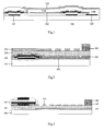
Fig. 1 illustrates a cross section of a conventional array substrate; -
Fig. 2 illustrates a cross section of an array substrate in accordance with an embodiment of the invention; and -
Fig. 3 illustrates a cross section of an array substrate in accordance with another embodiment of the invention. - In order to make objects, technical details and advantages of the embodiments of the invention apparent, the technical solutions of the embodiment will be described in a clearly and fully understandable way in connection with the drawings related to the embodiments of the invention. It is obvious that the described embodiments are just a part but not all of the embodiments of the invention. Based on the described embodiments herein, those skilled in the art can obtain other embodiment(s), without any inventive work, which should be within the scope of the invention.
- According to the invention, considering that VHR is most influenced by the parasitic capacitance, the parasitic capacitance is maximized within the reasonable range such that VHR may be maintained as high as possible without affecting the aperture ratio and introducing additional TFTs and corresponding signal lines in the substrate.
- As illustrated in
Fig. 2 , an embodiment of the invention is described with reference to an example of an ADvanced Super Dimension Switch (ADS) mode array substrate (a FFS mode array substrate may be also used herein). The array substrate comprises: a TFT 202 (bottom-gate) disposed on asubstrate 201, apixel electrode layer 203 driven by theTFT 202, a gate line (not shown in the figure), a data line 206 (formed at the same time as source/drain of the TFT), afirst passivation layer 204, asecond passivation layer 207 and acommon electrode layer 205. In the embodiment, thecommon electrode layer 205 comprises strip common electrodes and disposed over thepixel electrode 203. The gate line is used for switch on/off the driving of theTFT 202; a signal on the data line 206 is transmitted to thepixel electrode layer 203 via theTFT 202; thefirst passivation layer 204 is disposed on theTFT 202 and thepixel electrode layer 203. Thesecond passivation layer 207 is disposed between thecommon electrode layer 205 and the data line 206, that is, located on thefirst passivation layer 204 and in a corresponding region above the data line 206. - The
substrate 201 is for example a glass substrate. Thepixel electrode layer 203 and thecommon electrode layer 205 are for example transparent oxide film, such as ITO (Indium tin oxide), IZO (Indium zinc oxide) and the like. A pattern and position of thepixel electrode layer 203 and thecommon electrode layer 205 are disposed according to the conventional ADS mode, that is, the common electrode is disposed above the data line 206 and shields the electric field between the data line 206 and the pixel electrode, thereby improving the aperture ratio. The TFT comprises gate (G), source (S) and drain (D), source (S) of the TFT is electrically connected to the pixel electrode, gate S of the TFT is electrically connected to the gate line. - For the purpose of achieving a large storage capacitance, in the array substrate as illustrated in
Fig. 2 a thickness of thefirst passivation layer 204 may be configured according to the needed storage capacitance. That is, the thickness of thefirst passivation layer 204 between thepixel electrode layer 203 and thecommon electrode layer 205 may be decreased from the present 6500Å according to the desired frequency, thereby increasing the storage capacitance between the pixel electrode and the common electrode. However, when the thickness of thefirst passivation layer 204 is reduced, a distance between the data line 206 and thecommon electrode layer 205 is decreased, thereby forming a large parasitic capacitor between the data line 206 and thecommon electrode layer 205, which would influence the normal function of the data line 206. In this case, thesecond passivation layer 207 is disposed between the data line 206 and thecommon electrode layer 205 so as to decrease the parasitic capacitor between the data line 206 and thecommon electrode layer 205. Thesecond passivation layer 207 is used to further separate the data line 206 and thecommon electrode layer 205 by a distance such that influence from the capacitor in-between is minimized. The storage capacitance formed between the pixel electrode and the common electrode can be controlled through the thickness of thefirst passivation layer 204, and the parasitic capacitance between the common electrode and the data line can be controlled through the thickness of thesecond passivation layer 207. Moreover, the thicknesses of the first andsecond passivation layers second passivation layer 207 is for example made of resin or silicon nitrides (SiNx), with a thickness of for example 1500Å ∼5000Å. Thefirst passivation layer 204 may be of the same material as thesecond passivation layer 207 and with a thickness of for example less than 6500Å. - Another typical ADS array substrate as illustrated in
Fig. 3 is provided according to another embodiment of the invention. The array substrate comprises asubstrate 301, acommon electrode layer 305 directly overlaying thesubstrate 301, afirst passivation layer 304 disposed on thecommon electrode layer 305, the TFT 302 (top gate) disposed on thefirst passivation layer 304 and apixel electrode layer 303. Thesecond passivation layer 307 is disposed between thecommon electrode layer 305 and thedata line 306, that is, located on thefirst passivation layer 304 and in a corresponding region below thedata line 306. - In the embodiment, the
second passivation layer 307 is disposed between thedata line 306 and thecommon electrode layer 305, which are further separated by thesecond passivation layer 307 by a distance. In this way, the storage capacitance formed between the pixel electrode and the common electrode can be controlled through the thickness of thefirst passivation layer 304, and the parasitic capacitance between the common electrode and the data line can be controlled through the thickness of thesecond passivation layer 307. Moreover, the thicknesses of the first and second passivation layers 304 and 307 can be controlled separately. - It is noted that the above embodiments are described in related to a pixel unit of the array substrate, it is well-known in the art that the array substrate consists of a plurality of pixel units, each of which comprises a same TFT as above mentioned.
- Still another embodiment of the invention provides a display device comprising the above array substrate. The display device may be a LC panel, an E-paper, an OLED panel, a plasma panel, a LC television, a LCD, a digital photo-frame, a mobile phone, a tablet PC and any product or component having a display function.
- In the above embodiments of the invention, the parasitic capacitance of the pixel electrode is increased by adjusting the thickness of the first passivation layer between the pixel electrode layer and the common electrode layer, thereby maintaining VHR of the pixel electrode above a certain level. As a result, screen flicker will not be induced by too low VHR when dynamically decreasing the drive frequency of the LCD. As no elements and its corresponding lines for controlling the parasitic capacitance is needed, the aperture ratio is not affected, thereby guaranteeing the display quality. Moreover, the data line and the common electrode is further separated by a distance by using the second passivation layer, and the capacitance therebetween is minimized, thereby ensuing normal function of the data line.
- What are described above is related to the illustrative embodiments of the disclosure only and not limitative to the scope of the disclosure; the scopes of the disclosure are defined by the accompanying claims.
Claims (7)
- An array substrate, comprising: a TFT (202, 302), a pixel electrode layer (203, 303) driven by the TFT (202, 302), a data line (206, 306), a first passivation layer (204, 304) and a common electrode layer (205, 305) disposed on a substrate (201, 301), the data line (206, 306) is for driving the TFT (202, 302), the first passivation layer (204, 304) is disposed between the pixel electrode layer (203, 303) and the common electrode layer (205, 305), wherein the array substrate further comprises a second passivation layer (207, 307) disposed between the common electrode layer (205, 305) and the data line (206, 306) and located in a region corresponding to the data line (206, 306).
- The array substrate of claim 1, wherein the first passivation layer (204) is disposed on the TFT (202), the pixel electrode layer (203) and the data line (206); the second passivation layer (207) is disposed on the first passivation layer (204) and located in a region above the data line (206); the common electrode layer (205) is disposed on the first passivation layer (204) and the second passivation layer (207).
- The array substrate of claim 1, wherein the common electrode layer (305) directly overlays the substrate (301); the first passivation layer (304) is disposed on the common electrode layer (305); the TFT (302), the pixel electrode layer (303) and the data line (306) are disposed on the first passivation layer (304); the second passivation layer (307) is disposed on the first passivation layer (304) and located in a region below the data line (306).
- The array substrate of any of claims 1 to 3, wherein a thickness of the first passivation layer (204, 304) is less than 6500Å.
- The array substrate of any of claims 1 to 4, wherein a thickness of the second passivation layer (207, 307) is 1500Å ∼5000Å.
- The array substrate of any of claims 1 to 5, wherein the second passivation layer (204, 304) is made of resin or silicon nitrides.
- A display device comprising the array substrate of any of claims 1 to 6.
Applications Claiming Priority (1)
| Application Number | Priority Date | Filing Date | Title |
|---|---|---|---|
| CN2013100312901A CN103064224A (en) | 2013-01-28 | 2013-01-28 | Arrayed substrate and display device |
Publications (1)
| Publication Number | Publication Date |
|---|---|
| EP2759875A1 true EP2759875A1 (en) | 2014-07-30 |
Family
ID=48106912
Family Applications (1)
| Application Number | Title | Priority Date | Filing Date |
|---|---|---|---|
| EP14150532.1A Withdrawn EP2759875A1 (en) | 2013-01-28 | 2014-01-09 | Array substrate and display device |
Country Status (3)
| Country | Link |
|---|---|
| US (1) | US9818762B2 (en) |
| EP (1) | EP2759875A1 (en) |
| CN (1) | CN103064224A (en) |
Families Citing this family (12)
| Publication number | Priority date | Publication date | Assignee | Title |
|---|---|---|---|---|
| CN103915431B (en) * | 2013-06-17 | 2017-10-20 | 上海天马微电子有限公司 | TFT array substrate, display device and array substrate manufacturing method |
| CN103969865B (en) | 2013-10-10 | 2017-10-27 | 上海中航光电子有限公司 | Tft array substrate and its manufacture method, display panel and display device |
| CN104122701A (en) * | 2014-07-28 | 2014-10-29 | 深圳市华星光电技术有限公司 | Liquid crystal display panel, manufacturing method thereof and array substrate |
| CN104317122B (en) * | 2014-10-10 | 2018-01-12 | 上海中航光电子有限公司 | Dot structure, array base palte, display panel and display device and its driving method |
| CN105633096B (en) * | 2016-01-05 | 2018-09-18 | 深圳市华星光电技术有限公司 | Liquid crystal display panel, TFT substrate and its manufacturing method |
| CN107272291A (en) * | 2017-07-25 | 2017-10-20 | 武汉华星光电技术有限公司 | A kind of preparation method of array base palte, display panel and the array base palte |
| CN208848008U (en) | 2018-10-29 | 2019-05-10 | 惠科股份有限公司 | Substrate and display panel |
| CN110412805A (en) * | 2019-07-29 | 2019-11-05 | 昆山龙腾光电有限公司 | Array substrate and preparation method thereof, liquid crystal display device |
| CN113724595B (en) * | 2021-08-30 | 2023-10-13 | 京东方科技集团股份有限公司 | display panel |
| CN114415408A (en) * | 2022-01-21 | 2022-04-29 | 合肥京东方显示技术有限公司 | Display substrate, preparation method thereof and display device |
| CN115390302A (en) | 2022-08-23 | 2022-11-25 | 广州华星光电半导体显示技术有限公司 | Liquid crystal display panel and preparation method thereof |
| CN120089085A (en) * | 2025-03-03 | 2025-06-03 | 武汉华星光电技术有限公司 | Display device and driving method thereof |
Citations (7)
| Publication number | Priority date | Publication date | Assignee | Title |
|---|---|---|---|---|
| US20020149729A1 (en) * | 2001-02-28 | 2002-10-17 | Etsuko Nishimura | Liquid crystal display apparatus |
| US20030071931A1 (en) * | 2001-10-15 | 2003-04-17 | Hitachi, Ltd. | Liquid crystal display device, display device and manufacturing method thereof |
| JP2004062145A (en) * | 2002-04-04 | 2004-02-26 | Nec Lcd Technologies Ltd | In-plane switching type active matrix liquid crystal display device and method of manufacturing the same |
| US20060158597A1 (en) * | 2005-01-17 | 2006-07-20 | Nec Lcd Technologies, Ltd. | In-plane switching liquid crystal display device |
| US20070273819A1 (en) * | 2006-05-25 | 2007-11-29 | Nec Lcd Technologies, Ltd. | High aperture ratio in-plane switching mode active matrix liquid crystal display unit |
| US20120113080A1 (en) * | 2010-11-04 | 2012-05-10 | Scanvue Technologies, Llc | Thin-Film Transistor Liquid-Crystal Display with Variable Frame Frequency |
| EP2472310A1 (en) * | 2011-01-03 | 2012-07-04 | Samsung Electronics Co., Ltd. | Fringe field switching liquid crystal display and manufacturing method thereof |
Family Cites Families (12)
| Publication number | Priority date | Publication date | Assignee | Title |
|---|---|---|---|---|
| JP2622183B2 (en) * | 1990-04-05 | 1997-06-18 | シャープ株式会社 | Active matrix display device |
| JP2821347B2 (en) * | 1993-10-12 | 1998-11-05 | 日本電気株式会社 | Current control type light emitting element array |
| US5657101A (en) * | 1995-12-15 | 1997-08-12 | Industrial Technology Research Institute | LCD having a thin film capacitor with two lower capacitor electrodes and a pixel electrode serving as an upper electrode |
| US6940566B1 (en) * | 1996-11-26 | 2005-09-06 | Samsung Electronics Co., Ltd. | Liquid crystal displays including organic passivation layer contacting a portion of the semiconductor layer between source and drain regions |
| US6252290B1 (en) * | 1999-10-25 | 2001-06-26 | Chartered Semiconductor Manufacturing Ltd. | Method to form, and structure of, a dual damascene interconnect device |
| US6933528B2 (en) * | 2002-04-04 | 2005-08-23 | Nec Lcd Technologies, Ltd. | In-plane switching mode active matrix type liquid crystal display device and method of fabricating the same |
| JP2004191627A (en) * | 2002-12-11 | 2004-07-08 | Hitachi Ltd | Organic light emitting display |
| KR101107252B1 (en) * | 2004-12-31 | 2012-01-19 | 엘지디스플레이 주식회사 | Thin film transistor substrate of electroluminescent display panel and manufacturing method thereof |
| US7847904B2 (en) * | 2006-06-02 | 2010-12-07 | Semiconductor Energy Laboratory Co., Ltd. | Liquid crystal display device and electronic appliance |
| DE102011053665B4 (en) * | 2010-09-20 | 2016-06-30 | Lg Display Co., Ltd. | An organic light emitting diode display device and method of manufacturing the same |
| US8659734B2 (en) | 2011-01-03 | 2014-02-25 | Samsung Display Co., Ltd. | Liquid crystal display and manufacturing method thereof |
| TW201245829A (en) * | 2011-05-05 | 2012-11-16 | Au Optronics Corp | Pixel structure and method for fabricating the same |
-
2013
- 2013-01-28 CN CN2013100312901A patent/CN103064224A/en active Pending
- 2013-12-10 US US14/101,881 patent/US9818762B2/en active Active
-
2014
- 2014-01-09 EP EP14150532.1A patent/EP2759875A1/en not_active Withdrawn
Patent Citations (7)
| Publication number | Priority date | Publication date | Assignee | Title |
|---|---|---|---|---|
| US20020149729A1 (en) * | 2001-02-28 | 2002-10-17 | Etsuko Nishimura | Liquid crystal display apparatus |
| US20030071931A1 (en) * | 2001-10-15 | 2003-04-17 | Hitachi, Ltd. | Liquid crystal display device, display device and manufacturing method thereof |
| JP2004062145A (en) * | 2002-04-04 | 2004-02-26 | Nec Lcd Technologies Ltd | In-plane switching type active matrix liquid crystal display device and method of manufacturing the same |
| US20060158597A1 (en) * | 2005-01-17 | 2006-07-20 | Nec Lcd Technologies, Ltd. | In-plane switching liquid crystal display device |
| US20070273819A1 (en) * | 2006-05-25 | 2007-11-29 | Nec Lcd Technologies, Ltd. | High aperture ratio in-plane switching mode active matrix liquid crystal display unit |
| US20120113080A1 (en) * | 2010-11-04 | 2012-05-10 | Scanvue Technologies, Llc | Thin-Film Transistor Liquid-Crystal Display with Variable Frame Frequency |
| EP2472310A1 (en) * | 2011-01-03 | 2012-07-04 | Samsung Electronics Co., Ltd. | Fringe field switching liquid crystal display and manufacturing method thereof |
Also Published As
| Publication number | Publication date |
|---|---|
| US9818762B2 (en) | 2017-11-14 |
| US20140209935A1 (en) | 2014-07-31 |
| CN103064224A (en) | 2013-04-24 |
Similar Documents
| Publication | Publication Date | Title |
|---|---|---|
| US9818762B2 (en) | Arrangement of passivation layers in a pixel unit of an array substrate and display device | |
| CN102737597B (en) | Liquid crystal display device having a plurality of pixel electrodes | |
| US10809551B2 (en) | Liquid crystal display device having switchable viewing angles and viewing angle switching method thereof | |
| US10585320B2 (en) | Array substrate and driving method and manufacturing method thereof | |
| CN102929054B (en) | Array substrate and driving method of pixels | |
| JP5654677B2 (en) | Liquid crystal display panel and liquid crystal display device | |
| US7532269B2 (en) | Liquid crystal displays | |
| KR20090123738A (en) | Display panel and liquid crystal display including same and manufacturing method thereof | |
| US9323123B2 (en) | Structure of pixel | |
| US9984649B2 (en) | Array substrate, driving method thereof and display device | |
| CN104272176B (en) | Liquid crystal driving method and liquid crystal display device | |
| GB2533512A (en) | Pixel structure and method of manufacturing same | |
| US20090015741A1 (en) | Liquid crystal display and method of driving the same | |
| US10281786B2 (en) | Display device using low capacitance bus lines having gate lines and data lines on different substrates | |
| KR20120104721A (en) | Liquid crystal display and driving method thereof | |
| US20140240268A1 (en) | Thin-film transistor liquid-crystal display with variable frame frequency | |
| US20190012975A1 (en) | Pixel circuit structure and display panel | |
| US9417497B1 (en) | TFT array substrate structure | |
| CN203324618U (en) | Array substrate and display device | |
| JP2016031464A (en) | Liquid crystal display device and driving method thereof | |
| WO2008007610A1 (en) | Liquid crystal display device | |
| CN220105484U (en) | Array substrate and display device | |
| US20250053033A1 (en) | Display device | |
| JP2006091288A (en) | LCD panel | |
| KR101232149B1 (en) | Liquid Crystal Display Device And Method For Fabricating The Same |
Legal Events
| Date | Code | Title | Description |
|---|---|---|---|
| PUAI | Public reference made under article 153(3) epc to a published international application that has entered the european phase |
Free format text: ORIGINAL CODE: 0009012 |
|
| 17P | Request for examination filed |
Effective date: 20140109 |
|
| AK | Designated contracting states |
Kind code of ref document: A1 Designated state(s): AL AT BE BG CH CY CZ DE DK EE ES FI FR GB GR HR HU IE IS IT LI LT LU LV MC MK MT NL NO PL PT RO RS SE SI SK SM TR |
|
| AX | Request for extension of the european patent |
Extension state: BA ME |
|
| STAA | Information on the status of an ep patent application or granted ep patent |
Free format text: STATUS: THE APPLICATION IS DEEMED TO BE WITHDRAWN |
|
| 18D | Application deemed to be withdrawn |
Effective date: 20150131 |