EP2759832A1 - Electrochemical sensor device - Google Patents
Electrochemical sensor device Download PDFInfo
- Publication number
- EP2759832A1 EP2759832A1 EP13152411.8A EP13152411A EP2759832A1 EP 2759832 A1 EP2759832 A1 EP 2759832A1 EP 13152411 A EP13152411 A EP 13152411A EP 2759832 A1 EP2759832 A1 EP 2759832A1
- Authority
- EP
- European Patent Office
- Prior art keywords
- electrochemical sensor
- electrodes
- integrated
- sensor element
- integrated circuit
- Prior art date
- Legal status (The legal status is an assumption and is not a legal conclusion. Google has not performed a legal analysis and makes no representation as to the accuracy of the status listed.)
- Granted
Links
Images




Classifications
-
- G—PHYSICS
- G01—MEASURING; TESTING
- G01N—INVESTIGATING OR ANALYSING MATERIALS BY DETERMINING THEIR CHEMICAL OR PHYSICAL PROPERTIES
- G01N27/00—Investigating or analysing materials by the use of electric, electrochemical, or magnetic means
- G01N27/26—Investigating or analysing materials by the use of electric, electrochemical, or magnetic means by investigating electrochemical variables; by using electrolysis or electrophoresis
-
- G—PHYSICS
- G01—MEASURING; TESTING
- G01N—INVESTIGATING OR ANALYSING MATERIALS BY DETERMINING THEIR CHEMICAL OR PHYSICAL PROPERTIES
- G01N27/00—Investigating or analysing materials by the use of electric, electrochemical, or magnetic means
- G01N27/26—Investigating or analysing materials by the use of electric, electrochemical, or magnetic means by investigating electrochemical variables; by using electrolysis or electrophoresis
- G01N27/403—Cells and electrode assemblies
- G01N27/404—Cells with anode, cathode and cell electrolyte on the same side of a permeable membrane which separates them from the sample fluid, e.g. Clark-type oxygen sensors
- G01N27/4045—Cells with anode, cathode and cell electrolyte on the same side of a permeable membrane which separates them from the sample fluid, e.g. Clark-type oxygen sensors for gases other than oxygen
-
- G—PHYSICS
- G01—MEASURING; TESTING
- G01N—INVESTIGATING OR ANALYSING MATERIALS BY DETERMINING THEIR CHEMICAL OR PHYSICAL PROPERTIES
- G01N33/00—Investigating or analysing materials by specific methods not covered by groups G01N1/00 - G01N31/00
- G01N33/0004—Gaseous mixtures, e.g. polluted air
- G01N33/0009—General constructional details of gas analysers, e.g. portable test equipment
- G01N33/0027—General constructional details of gas analysers, e.g. portable test equipment concerning the detector
- G01N33/0036—General constructional details of gas analysers, e.g. portable test equipment concerning the detector specially adapted to detect a particular component
- G01N33/004—CO or CO2
Definitions
- This invention relates to an electrochemical sensor device for use in the detection of components in a gaseous medium.
- Electrochemical sensors are well known in the art for use in the detection of components in a gaseous medium.
- the sensors generally comprise at least two electrodes, a working electrode and a counter electrode.
- the change in electrical impedance between the electrodes is determined, for example by applying a voltage of known value and form across the electrodes, as a result of the sensor being brought into contact with the gaseous medium.
- the electrodes are coated with an electrolytic or semiconductor material that bridges the electrodes, the apparent conductivity of which changes as a result of contact with the gaseous medium.
- Electrochemical gas sensors are used in a wide variety of applications e.g. for safety (detection of toxic gas concentrations) or environmental monitoring.
- an electrochemical sensor device according to claim 1.
- Embodiments may further comprise a filter to increase the selectivity of the electrochemical sensor element.
- a reference electrode may be formed on the upper surface of the substrate below the electrolyte layer.
- the thickness of the electrolyte layer may be 10 ⁇ m or less, and the area of the first and second electrodes electrically contacting the electrolyte layer may be in the range of 0.01 mm 2 to 11 mm 2 .
- Embodiments may provide a packaged electrochemical sensor device having an integrated electrochemical sensor element and sensor integrated circuit formed on a single die.
- the integrated electrochemical sensor element and the sensor integrated circuit may be formed on separate dies but provided in a single package (e.g. packaged in the same discrete component).
- embodiments may provide a packaged gas sensor device that comprises an electrochemical sensor element and an electrical read-out circuit integrated within the single package. Co-integration of the sensor element and read-out electronics in the same discrete package may enable considerable reduction in overall system size and cost.
- the electrochemical sensor and electrical read-out circuit may be further integrated on top of a conventional CMOS chip or die.
- embodiments may provide for the integration of an electrochemical sensor element together with the read-out electronics in a single discrete package. This may be done using two separate dies (one for the electrochemical sensor element and the other for a read-out integrated circuit (IC)) and electrically connecting the separate dies by bond wires.
- the electrochemical sensor element may be manufactured on the same die as the read-out IC to provide an even smaller form factor whilst using CMOS processes.
- additional processing steps may only be needed after undertaking conventional processing, thus avoiding changes to existing processes.
- Additional sensor elements adapted to sense of parameters such as temperature, relative humidity, ambient light etc. may also be included in the same package. Such further sensors may be used to provide additional environmental information, and may also be used to correct for altered sensitivity of the electrochemical sensor element (due to temperature or relative humidity for example) thereby improving the accuracy of an electrochemical sensor device according to an embodiment.
- chip integrated circuit
- monolithic device semiconductor device, and microelectronic device
- present invention is applicable to all the above as they are generally understood in the field.
- metal line interconnect line, trace, wire, conductor, signal path and signalling medium are all related. The related terms listed above, are generally interchangeable, and appear in order from specific to general. In this field, metal lines are sometimes referred to as traces, wires, lines, interconnect or simply metal. Metal lines, generally aluminum (Al), copper (Cu) or an alloy of Al and Cu, are conductors that provide signal paths for coupling or interconnecting, electrical circuitry. Conductors other than metal are available in microelectronic devices.
- doped polysilicon doped single-crystal silicon (often referred to simply as diffusion, regardless of whether such doping is achieved by thermal diffusion or ion implantation), titanium (Ti), molybdenum (Mo), and refractory metals are examples of other conductors.
- contact and via both refer to structures for electrical connection of conductors at different interconnect levels. These terms are sometimes used in the art to describe both an opening in an insulator in which the structure will be completed, and the completed structure itself. For purposes of this disclosure contact and via refer to the completed structure.
- vertical means substantially orthogonal to the surface of a substrate. Also, terms describing positioning or location (such as above, below, top, bottom, etc) are to be construed in conjunction with the orientation of the structures illustrated in the diagrams.
- the relation between electric current and gas concentration in air will now be analysed.
- the measured current is a combination of three processes.
- a short analysis is included, resulting in a formula to estimate the maximum obtainable current for a given electrode surface area, gas concentration and electrolyte thickness.
- This concentration will always exist at the air-electrolyte interface (see label “(1)” in Figure 1 ). In the absence of electrochemical processes (e.g. at open circuit potential), the concentration will be uniform throughout the electrolyte and at the electrode surfaces by diffusion of the gas molecules (see label “(2)" in Figure 1 ). The gas molecules are the electrochemically active species in this system.
- E mix E 0 CO + E 0 O 2 2 - 59.6 ⁇ mV n ⁇ log ⁇ CO O 2 1 / 2
- E 0 CO and E 0 O2 are the standard electrode potentials for CO and O 2 (-0.11 and +0.4 V vs. SHE), respectively
- i l nFAD CO ⁇ c CO ⁇
- n the number of electrons involved in the reaction
- F Faraday's constant
- A the electrode surface area
- D CO the diffusion constant of CO in the electrolyte
- C CO the concentration of CO molecules at the air-electrolyte
- Equation 1 nFAD CO ⁇ ⁇ p CO k H - p CO ⁇ c solvent
- the minimal form factor A(electrode)/ ⁇ (electrolyte) can be calculated.
- the minimal electrode surface area for a 10 ⁇ m thick electrolyte is also shown in Table 1. It has therefore been identified that a minimal electrode surface area of 0.16mm 2 to 1.1mm 2 may be required to detect 5 ppm CO for a 10 ⁇ m thick electrolyte. For these electrolytes, further downscaling can be achieved by decreasing the electrolyte thickness or increasing the resolution and accuracy of the current measurement circuit
- the electrochemical sensor device 10 comprises an integrated electrochemical sensor element 12 according to an embodiment of the invention and a sensor integrated circuit (IC) (or CMOS chip) 14 electrically connected to the integrated electrochemical sensor element 12.
- IC sensor integrated circuit
- the integrated electrochemical sensor element comprises first 16 and second 18 electrodes formed on the upper surface of a substrate 20, and an electrolyte 19 formed on the first 16 and second 18 electrodes so as to electrically contact both the first 16 and second 18 electrodes.
- the first 16 and second 18 electrodes are each electrically connected to the sensor IC 14 via respective bond wires 22A and 22B.
- the first 16 and second 18 electrodes are formed from Platinum (Pt), although it will be understood that other suitable materials made be used for the electrodes, such as Au and Pd for example (in addition Ag or AgCl may be used as material for reference electrodes).
- the sensor IC 14 is connected to first 24 to third 26 input/output terminals of the packaged electrochemical sensor device 10 to provide for the input and/or output of signals to the sensor IC 14.
- the integrated electrochemical sensor element 12 and sensor IC 14 are provided on separate dies within the packaging of the device 10. In alternative embodiment, the integrated electrochemical sensor element 12 and sensor IC 14 may be formed on the same die.
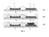
- FIG. 5 there is illustrated a method of manufacturing the device of Figure 4 , wherein the integrated electrochemical sensor element 12 and sensor IC 14 are provided on separate dies within the packaging of the device 10.
- the first 16 and second 18 electrodes of the electrochemical sensor element 12 are patterned on a glass substrate 20.
- a CMOS wafer (containing a plurality of sensor ICs) is diced into individual dies 30 each having a sensor IC 14 provided thereon.
- a second die 30 having a sensor IC 14 thereon is obtained.
- the first 28 and second 30 dies are attached to a lead frame/support 32, and the first 16 and second 18 electrodes are electrically connected to the sensor IC on the second die 30 via wire bonds 22 to provide the structure shown in Figure 5A .
- electrolyte 19 is then applied to electrochemical sensor element 12, for example by an inkjet or micro drop process to provide the structure shown in Figure 5C .
- the deposited electrolyte 19 contacts the first 16 and second 18 electrodes of the electrochemical sensor elements 12
- FIG. 6 a modification to the embodiment of Figure 4 is shown. More specifically, the method of embodiment of Figure 4 is modified to include a filter positioned directly above the electrolyte 19.
- FIG. 5C is modified by the addition of suitable structures 33 (e.g. rings) for attachment during overmolding (by adaptation of the molding form).
- suitable structures 33 e.g. rings
- FIG. 6A The addition of such structures is shown in Figure 6A .
- Individual filter layers 34 can be cut with a punch tool and applied (by a pick and place machine) above the electrolyte 19 (and within area defined by the structures 33). Moreover, a rigid yet transparent to gas material (e.g. polymer mesh or plate with holes) can be applied as the top layer for mechanical protection
- FIG. 7 there is illustrated a method of manufacturing a device according to an alternative embodiment, wherein the integrated electrochemical sensor element and sensor IC are provided on a single die.
- a die 70 with integrated sensor IC and bond pads 14 as shown in Figure 7A .
- the bond pads 14 are provided to cater for bond wire connections to be made to the integrated sensor IC (see Figure 7C )
- Pt electrodes are deposited on a substrate 72 and patterned using known techniques.
- the resultant structure is the attached to the die 70 to provide the die structure shown in Figure 7B , wherein the Pt electrodes are electrically connected to the sensor IC 14 via Tungsten vias (not shown).
- the Pt electrodes may be deposited and patterned directly on top of the die 70 (with electrodes connected to the underlying circuit by vias), so no extra substrate and die attach/stacking is needed.
- FIG. 7D Subsequent encapsulation e.g. by open cavity molding (overmolding) and curing is illustrated in Figure 7D , wherein the Pt electrodes on the substrate 72 are at least partially exposed.
- the sensor IC and the integrated electrochemical sensor element are at least partially encapsulated in resin, wherein a cavity is formed in the resin which exposes the electrodes of the integrated electrochemical sensor element.
- An electrolyte 19 is then applied to cover the exposed Pt electrodes, for example by an inkjet or micro drop process to provide the structure shown in Figure 7E .
- the deposited electrolyte 19 therefore contacts the electrode of the electrochemical sensor element.
- the embodiment of Figure 7 may be modified to further comprise one or more filters positioned directly above the electrolyte 19.
- a plurality of integrated electrochemical sensor elements may be provided within a single discrete package (either on the same die or on separate dies).
- electrolyte volume in an electrochemical sensor element may be very small.
- ionic liquids which have low vapour pressure, and thus reduced evaporation ability
- solid electrolytes may be used as an electrolyte in an embodiment.
- one of the filter layers may be chosen so at to restrict or prevent electrolyte evaporation.
- first and second electrodes i.e. the working and counter electrodes
- An electrochemical sensor element according to an embodiment of the invention may also comprise a third electrode (commonly referred to as a reference electrode) in contact with the electrolyte.
- the working and counter electrodes may be made from Platinum (Pt) while the reference electrode may be made from Ag/AgCl. It will be understood, however, that other metals may be used depending on the chemical reactions involved.
- FIG. 8 there is illustrated a method of manufacturing an integrated electrochemical sensor element for a device according to an alternative embodiment.
- a substrate 80 as shown in Figure 8A .
- the substrate 80 is then etched so as to form a cavity 82 in the upper surface of the substrate 80 as shown in Figure 8B .
- Pt electrodes 84 are deposited on the substrate 82 within the cavity 82 and patterned using known techniques.
- the resultant structure is shown in Figure 7C , wherein the Pt electrodes 84 are situated in the cavity 84 of the substrate 84.
- An electrolyte 86 is then deposited to fill the cavity 82 and cover the electrodes 84 as shown in Figure 7D .
- the deposited electrolyte 86 therefore covers and contacts the electrodes 84 of the electrochemical sensor element.
- the cavities, electrodes and electrolyte of electrochemical sensor elements according to embodiments may be processed on a wafer-scale, thereby helping to decrease the cost of manufacturing.
- FIG. 9 A modification to the method of Figure 8 is illustrated in Figure 9 , wherein a cavity is not formed in the substrate but, instead, a solid electrolyte is deposited over the electrode and patterned by photo-litho.
- a substrate 80 as shown in Figure 9A .
- Pt electrodes 84 are deposited on the upper surface of the substrate 80 and patterned using known techniques to provide the structure shown in Figure 9B .
- a solid electrolyte 88 is then deposited to cover the upper surface of the substrate 80 and the electrodes 84 as shown in Figure 9C .
- the deposited electrolyte 88 therefore covers and contacts the electrodes 84 of the electrochemical sensor element.
- the electrolyte 88 is patterned by photo-lithography so to remove one or more portions of the electrolyte 88 and provide the final structure as shown in Figure 9D .
- the modified method shown in Figure 9 enables processing at the wafer level. Accordingly, an electrochemical sensor element manufactured according to such a method may be cheap (due to mass-production. Further, this type of processing is possible "on-top of" CMOS or can be fabricated on a separate die and subsequently be packaged together with the read-out electronics (e.g. sensor IC).
- any other suitable insulating substrate such as a Si substrate for example.
- a Si substrate is semiconducting which may cause direct currents between electrodes through substrate.
- a dielectric insulation layer e.g. SiO 2 or SiN
- the electrodes can then be patterned on top of the insulation layer.
- planar electrode arrangements may be suitable, since this can be easily achieved with conventional semiconductor technologies.
- the electrode may be formed in special shapes, such a meanders, rings, etc.
Landscapes
- Chemical & Material Sciences (AREA)
- Life Sciences & Earth Sciences (AREA)
- Health & Medical Sciences (AREA)
- Pathology (AREA)
- General Physics & Mathematics (AREA)
- Immunology (AREA)
- Physics & Mathematics (AREA)
- Analytical Chemistry (AREA)
- Biochemistry (AREA)
- General Health & Medical Sciences (AREA)
- Engineering & Computer Science (AREA)
- Chemical Kinetics & Catalysis (AREA)
- Electrochemistry (AREA)
- Molecular Biology (AREA)
- Combustion & Propulsion (AREA)
- Food Science & Technology (AREA)
- Medicinal Chemistry (AREA)
- Measuring Oxygen Concentration In Cells (AREA)
Abstract
Description
- This invention relates to an electrochemical sensor device for use in the detection of components in a gaseous medium.
- Electrochemical sensors are well known in the art for use in the detection of components in a gaseous medium. The sensors generally comprise at least two electrodes, a working electrode and a counter electrode. The change in electrical impedance between the electrodes is determined, for example by applying a voltage of known value and form across the electrodes, as a result of the sensor being brought into contact with the gaseous medium. In many cases, the electrodes are coated with an electrolytic or semiconductor material that bridges the electrodes, the apparent conductivity of which changes as a result of contact with the gaseous medium.
- Electrochemical gas sensors are used in a wide variety of applications e.g. for safety (detection of toxic gas concentrations) or environmental monitoring.
- Conventional electrochemical sensors are, however, typically large in size and expensive. This is primarily due to the separate electrochemical cell and read-out electronics which need to be connected by a Printed Circuit Board (PCB). Furthermore, in order to achieve sufficient sensor accuracy, the electrochemical sensor element should be large enough to generate sufficient current for measurement by the (typically distant) read-out electronics. This also contributes to the size of conventional electrochemical sensors.
- According to an aspect of the invention, there is provided an electrochemical sensor device according to
claim 1. - Embodiments may further comprise a filter to increase the selectivity of the electrochemical sensor element.
- A reference electrode may be formed on the upper surface of the substrate below the electrolyte layer.
- The thickness of the electrolyte layer may be 10µm or less, and the area of the first and second electrodes electrically contacting the electrolyte layer may be in the range of 0.01 mm2 to 11 mm2.
- Embodiments may provide a packaged electrochemical sensor device having an integrated electrochemical sensor element and sensor integrated circuit formed on a single die. In other embodiments, the integrated electrochemical sensor element and the sensor integrated circuit may be formed on separate dies but provided in a single package (e.g. packaged in the same discrete component).
- Thus, embodiments may provide a packaged gas sensor device that comprises an electrochemical sensor element and an electrical read-out circuit integrated within the single package. Co-integration of the sensor element and read-out electronics in the same discrete package may enable considerable reduction in overall system size and cost.
- The electrochemical sensor and electrical read-out circuit may be further integrated on top of a conventional CMOS chip or die.
- In other words, embodiments may provide for the integration of an electrochemical sensor element together with the read-out electronics in a single discrete package. This may be done using two separate dies (one for the electrochemical sensor element and the other for a read-out integrated circuit (IC)) and electrically connecting the separate dies by bond wires. Alternatively, the electrochemical sensor element may be manufactured on the same die as the read-out IC to provide an even smaller form factor whilst using CMOS processes. Here, additional processing steps may only be needed after undertaking conventional processing, thus avoiding changes to existing processes.
- Additional sensor elements adapted to sense of parameters such as temperature, relative humidity, ambient light etc. may also be included in the same package. Such further sensors may be used to provide additional environmental information, and may also be used to correct for altered sensitivity of the electrochemical sensor element (due to temperature or relative humidity for example) thereby improving the accuracy of an electrochemical sensor device according to an embodiment.
- Examples of the invention will now be described in detail with reference to the accompanying drawings, in which:
-
Figure 1 illustrates an initial equilibrium situation within an electrochemical sensor element for the electrochemically active gases involved in carbon monoxide sensing; -
Figures 2A-2C illustrate the various concentration profile for various values of externally applied potential difference; -
Figure 3 illustrates a full current situation within an electrochemical sensor element for the electrochemically active gases involved in carbon monoxide sensing; -
Figure 4 illustrates an electrochemical sensor device according to an embodiment of the invention; -
Figures 5A-5C show the steps of manufacturing the device ofFigure 4 ; -
Figures 6A-6B show a modification to the embodiment ofFigure 4 ; -
Figures 7A-7E illustrate the steps of manufacturing a device according to an alternative embodiment; -
Figures 8A-8D illustrate a method of manufacturing an integrated electrochemical sensor element for a device according to an embodiment; and -
Figures 9A-9D illustrate a method of manufacturing an integrated electrochemical sensor element for a device according to an alternative embodiment. - The terms, chip, integrated circuit, monolithic device, semiconductor device, and microelectronic device, are often used interchangeably in this field. The present invention is applicable to all the above as they are generally understood in the field.
- The terms metal line, interconnect line, trace, wire, conductor, signal path and signalling medium are all related. The related terms listed above, are generally interchangeable, and appear in order from specific to general. In this field, metal lines are sometimes referred to as traces, wires, lines, interconnect or simply metal. Metal lines, generally aluminum (Al), copper (Cu) or an alloy of Al and Cu, are conductors that provide signal paths for coupling or interconnecting, electrical circuitry. Conductors other than metal are available in microelectronic devices. Materials such as doped polysilicon, doped single-crystal silicon (often referred to simply as diffusion, regardless of whether such doping is achieved by thermal diffusion or ion implantation), titanium (Ti), molybdenum (Mo), and refractory metals are examples of other conductors.
- The terms contact and via, both refer to structures for electrical connection of conductors at different interconnect levels. These terms are sometimes used in the art to describe both an opening in an insulator in which the structure will be completed, and the completed structure itself. For purposes of this disclosure contact and via refer to the completed structure.
- The term vertical, as used herein, means substantially orthogonal to the surface of a substrate. Also, terms describing positioning or location (such as above, below, top, bottom, etc) are to be construed in conjunction with the orientation of the structures illustrated in the diagrams.
- There is proposed an integrated electrochemical sensor element that may be manufactured using IC processing techniques, thereby enabling a significant reduction in size when compared to conventional electrochemical sensors.
- To assess possible scaling of an electrochemical sensor element (or cell), the relation between electric current and gas concentration in air will now be analysed. In essence, the measured current is a combination of three processes. In the following section, a short analysis is included, resulting in a formula to estimate the maximum obtainable current for a given electrode surface area, gas concentration and electrolyte thickness.
- The initial equilibrium situation within an electrochemical sensor element is illustrated in
Figure 1 for the electrochemically active gases involved in carbon monoxide (CO) sensing. More specifically, the concentration of CO and O2 gas molecules in the electrolyte is in equilibrium with the gas partial pressure. In the pressure range of interest, this equilibrium concentration is directly proportional to the gas concentration. This is described by Henry's law (here shown for CO) in the following equation (Equation 1):
where pCO is the CO partial pressure, kH the Henry constant and xCO the mole fraction of CO in the solvent. The mole fraction can easily be recalculated into the concentration of CO using the following equation (Equation 2):
- This concentration will always exist at the air-electrolyte interface (see label "(1)" in
Figure 1 ). In the absence of electrochemical processes (e.g. at open circuit potential), the concentration will be uniform throughout the electrolyte and at the electrode surfaces by diffusion of the gas molecules (see label "(2)" inFigure 1 ). The gas molecules are the electrochemically active species in this system. When adsorbed at the electrode surface, they give rise to a mixed electrode potential which is determined by the Nernst law as described in the following equation (Equation 3):
wherein E0 CO and E0 O2 are the standard electrode potentials for CO and O2 (-0.11 and +0.4 V vs. SHE), respectively, and n is the number of electrons involved in the electrochemical reaction (here, n = 2). - Without any externally applied potential difference, the mixed electrode potential exists at both the sensing and counter electrode. This situation is represented by
Figure 2A . - Once a potential difference is applied between the sensing and counter electrodes, a new surface equilibrium concentration sets in (as described by the Nernst law). At the positively polarized electrode (i.e. the anode or sensing electrode), the CO molecules are oxidized into CO2, while O2 is reduced to OH- at the cathode (i.e. counter electrode). Up to moderate potential differences, it is the applied potential difference that determines the measured current. This regime, called the reaction limited regime, is represented by
Figure 2B . Because the measured current not only depends on the gas concentration in air but also on the applied potential, this regime is less suited for gas sensing. - Further increase of the potential difference decreases the surface concentration of gas molecules such that it comes close to zero. From this point onward, the reaction rate (the measured current) does not increase any more with an increasing potential difference. Instead, the current is limited by diffusion of CO molecules towards the electrodes. The resulting limiting current is the maximum current that can be obtained. This regime is represented in
Figure 2C . - The full current is now determined by the process of gas absorption (according to Henry's law) and diffusion towards the electrode, where CO is immediately oxidized. This limiting case is shown in more detail in
Figure 3 . - The limiting current il in this regime can be calculated by the following equation (Equation 3):

wherein n is the number of electrons involved in the reaction, F is Faraday's constant, A is the electrode surface area, DCO is the diffusion constant of CO in the electrolyte, CCO the concentration of CO molecules at the air-electrolyte - interface (determined by Henry's law), and δ the thickness of the electrolyte. Combining Henry's law (
Equation 1 and Equation 2) with the formula for the diffusion limiting current (Equation 3) gives the following equation (Equation 4) that allows for estimating the maximum current as a function of gas pressure:
- In Table 1 below, the material constants DCO, kH and Csolvent are detailed for two exemplary electrolytes, namely water (H2O) and an ionic liquid [Bmim][NTf2]. The data clearly shows that the mobility of CO molecules is higher in aqueous environments compared to the ionic liquid. However, the solubility of CO in the ionic liquid is higher.
DCO [m2/s] kH(CO) [atm] Csolvent [mole/m3] A [mm2] H2O 10e-10 58280 55.5e3 0.16 [Bmim][NTf2] 0.4e-10 950 3.4e3 1.1 - Using CMOS technology, it may be possible to resolve currents of about 15 pA. Assuming a minimal required resolution of 5 ppm CO and using the parameters for the example electrolytes above, the minimal form factor A(electrode)/δ(electrolyte) can be calculated. Thus, the minimal electrode surface area for a 10 µm thick electrolyte is also shown in Table 1. It has therefore been identified that a minimal electrode surface area of 0.16mm2 to 1.1mm2 may be required to detect 5 ppm CO for a 10µm thick electrolyte. For these electrolytes, further downscaling can be achieved by decreasing the electrolyte thickness or increasing the resolution and accuracy of the current measurement circuit
- Referring to
Figure 4 , there is illustrated a packagedelectrochemical sensor device 10 according to an embodiment of the invention. Theelectrochemical sensor device 10 comprises an integratedelectrochemical sensor element 12 according to an embodiment of the invention and a sensor integrated circuit (IC) (or CMOS chip) 14 electrically connected to the integratedelectrochemical sensor element 12. - The integrated electrochemical sensor element comprises first 16 and second 18 electrodes formed on the upper surface of a
substrate 20, and anelectrolyte 19 formed on the first 16 and second 18 electrodes so as to electrically contact both the first 16 and second 18 electrodes. The first 16 and second 18 electrodes are each electrically connected to thesensor IC 14 viarespective bond wires - The
sensor IC 14 is connected to first 24 to third 26 input/output terminals of the packagedelectrochemical sensor device 10 to provide for the input and/or output of signals to thesensor IC 14. - Here, the integrated
electrochemical sensor element 12 andsensor IC 14 are provided on separate dies within the packaging of thedevice 10. In alternative embodiment, the integratedelectrochemical sensor element 12 andsensor IC 14 may be formed on the same die. - Referring now to
Figure 5 , there is illustrated a method of manufacturing the device ofFigure 4 , wherein the integratedelectrochemical sensor element 12 andsensor IC 14 are provided on separate dies within the packaging of thedevice 10. Firstly, the first 16 and second 18 electrodes of theelectrochemical sensor element 12 are patterned on aglass substrate 20. provide on afirst die 28, and a CMOS wafer (containing a plurality of sensor ICs) is diced into individual dies 30 each having asensor IC 14 provided thereon. Thus, asecond die 30 having asensor IC 14 thereon is obtained. - The first 28 and second 30 dies are attached to a lead frame/
support 32, and the first 16 and second 18 electrodes are electrically connected to the sensor IC on thesecond die 30 via wire bonds 22 to provide the structure shown inFigure 5A . - Subsequent overmolding and curing (i.e. encapsulation) is illustrated in
Figure 5B . Here open cavity molding leaves a cavity directly on top of the first die 28). - An
electrolyte 19 is then applied toelectrochemical sensor element 12, for example by an inkjet or micro drop process to provide the structure shown inFigure 5C . The depositedelectrolyte 19 contacts the first 16 and second 18 electrodes of theelectrochemical sensor elements 12 - Turning now to
Figure 6 , a modification to the embodiment ofFigure 4 is shown. More specifically, the method of embodiment ofFigure 4 is modified to include a filter positioned directly above theelectrolyte 19. - Here, the structure shown in
Figure 5C is modified by the addition of suitable structures 33 (e.g. rings) for attachment during overmolding (by adaptation of the molding form). The addition of such structures is shown inFigure 6A . - Individual filter layers 34 can be cut with a punch tool and applied (by a pick and place machine) above the electrolyte 19 (and within area defined by the structures 33). Moreover, a rigid yet transparent to gas material (e.g. polymer mesh or plate with holes) can be applied as the top layer for mechanical protection
- Referring now to
Figure 7 , there is illustrated a method of manufacturing a device according to an alternative embodiment, wherein the integrated electrochemical sensor element and sensor IC are provided on a single die. - Firstly, there is provided a die 70 with integrated sensor IC and
bond pads 14 as shown inFigure 7A . Thebond pads 14 are provided to cater for bond wire connections to be made to the integrated sensor IC (seeFigure 7C ) - Next, Pt electrodes are deposited on a
substrate 72 and patterned using known techniques. The resultant structure is the attached to the die 70 to provide the die structure shown inFigure 7B , wherein the Pt electrodes are electrically connected to thesensor IC 14 via Tungsten vias (not shown). Alternatively the Pt electrodes may be deposited and patterned directly on top of the die 70 (with electrodes connected to the underlying circuit by vias), so no extra substrate and die attach/stacking is needed. - This is then attached to a lead frame/
support 74, and the sensor IC is electrically connected to the lead frame/support contacts viawire bonds 76 to provide the structure shown inFigure 7C . - Subsequent encapsulation e.g. by open cavity molding (overmolding) and curing is illustrated in
Figure 7D , wherein the Pt electrodes on thesubstrate 72 are at least partially exposed. For example, the sensor IC and the integrated electrochemical sensor element are at least partially encapsulated in resin, wherein a cavity is formed in the resin which exposes the electrodes of the integrated electrochemical sensor element. - An
electrolyte 19 is then applied to cover the exposed Pt electrodes, for example by an inkjet or micro drop process to provide the structure shown inFigure 7E . The depositedelectrolyte 19 therefore contacts the electrode of the electrochemical sensor element. - As with the embodiment comprising separate dies for the sensor IC and the electrochemical sensor element, the embodiment of
Figure 7 may be modified to further comprise one or more filters positioned directly above theelectrolyte 19. - Further, in alternative embodiments, a plurality of integrated electrochemical sensor elements may be provided within a single discrete package (either on the same die or on separate dies).
- It will be understood that the actual electrolyte volume in an electrochemical sensor element according to an embodiment may be very small. In order to prevent evaporation, ionic liquids (which have low vapour pressure, and thus reduced evaporation ability) or solid electrolytes may be used as an electrolyte in an embodiment. Alternatively, one of the filter layers may be chosen so at to restrict or prevent electrolyte evaporation.
- The embodiments described above have been detailed as having first and second electrodes (i.e. the working and counter electrodes). An electrochemical sensor element according to an embodiment of the invention may also comprise a third electrode (commonly referred to as a reference electrode) in contact with the electrolyte. In some embodiments, the working and counter electrodes may be made from Platinum (Pt) while the reference electrode may be made from Ag/AgCl. It will be understood, however, that other metals may be used depending on the chemical reactions involved.
- Referring now to
Figure 8 , there is illustrated a method of manufacturing an integrated electrochemical sensor element for a device according to an alternative embodiment. - Firstly, there is provided a
substrate 80 as shown inFigure 8A . Thesubstrate 80 is then etched so as to form acavity 82 in the upper surface of thesubstrate 80 as shown inFigure 8B . - Next,
Pt electrodes 84 are deposited on thesubstrate 82 within thecavity 82 and patterned using known techniques. The resultant structure is shown inFigure 7C , wherein thePt electrodes 84 are situated in thecavity 84 of thesubstrate 84. - An
electrolyte 86 is then deposited to fill thecavity 82 and cover theelectrodes 84 as shown inFigure 7D . The depositedelectrolyte 86 therefore covers and contacts theelectrodes 84 of the electrochemical sensor element. - This approach avoids the deposition of electrolyte on individually packaged sensor devices. Instead, the cavities, electrodes and electrolyte of electrochemical sensor elements according to embodiments may be processed on a wafer-scale, thereby helping to decrease the cost of manufacturing.
- A modification to the method of
Figure 8 is illustrated inFigure 9 , wherein a cavity is not formed in the substrate but, instead, a solid electrolyte is deposited over the electrode and patterned by photo-litho. Firstly, there is provided asubstrate 80 as shown inFigure 9A . Next,Pt electrodes 84 are deposited on the upper surface of thesubstrate 80 and patterned using known techniques to provide the structure shown inFigure 9B . Asolid electrolyte 88 is then deposited to cover the upper surface of thesubstrate 80 and theelectrodes 84 as shown inFigure 9C . The depositedelectrolyte 88 therefore covers and contacts theelectrodes 84 of the electrochemical sensor element. Finally, theelectrolyte 88 is patterned by photo-lithography so to remove one or more portions of theelectrolyte 88 and provide the final structure as shown inFigure 9D . - As for the embodiment of
Figure 8 , the modified method shown inFigure 9 enables processing at the wafer level. Accordingly, an electrochemical sensor element manufactured according to such a method may be cheap (due to mass-production. Further, this type of processing is possible "on-top of" CMOS or can be fabricated on a separate die and subsequently be packaged together with the read-out electronics (e.g. sensor IC). - Also, it is noted that although an embodiment described above (in conjunction with
Figure 5 ) has been detailed as employing a glass substrate, alternative embodiments may employ any other suitable insulating substrate, such as a Si substrate for example. A Si substrate, however, is semiconducting which may cause direct currents between electrodes through substrate. Thus, for such embodiments, it may be preferable to also employ a dielectric insulation layer (e.g. SiO2 or SiN) on top of the Si substrate prevent such currents. The electrodes can then be patterned on top of the insulation layer. - It is also noted that planar electrode arrangements may be suitable, since this can be easily achieved with conventional semiconductor technologies. Also, to increase the overall area of the electrodes, the electrode may be formed in special shapes, such a meanders, rings, etc.
- Various modifications will be apparent to those skilled in the art.
Claims (15)
- An electrochemical sensor device comprising:an integrated electrochemical sensor element having: a substrate; first and second electrodes formed on the upper surface of the substrate; and an electrolyte layer formed on the first and second electrodes so as to electrically contact both the first and second electrodes; anda sensor integrated circuit electrically connected to the first and second electrodes of the integrated electrochemical sensor element,wherein the integrated electrochemical sensor element and the sensor integrated circuit are provided in a single package.
- The electrochemical sensor device of claim 1, wherein the integrated electrochemical sensor element further comprises:a filter layer formed above the electrolyte layer, the filter layer being adapted to block one or more components of a gaseous medium.
- The electrochemical sensor device of claim 1 or 2, wherein the integrated electrochemical sensor element further comprises:a reference electrode formed on the upper surface of the substrate below the electrolyte layer, the electrolyte layer electrically contacting the reference electrode,and wherein the reference electrode is electrically connected to the integrated circuit.
- The electrochemical sensor device of any preceding claim, wherein the thickness of the electrolyte layer is 10µm or less,
and wherein the area of the first and second electrodes electrically contacting the electrolyte layer is 11 mm2 or less. - The electrochemical sensor device of any preceding claim, further comprising an overmould having a cavity situated above the integrated electrochemical sensor element, and wherein the electrolyte layer is formed in the cavity.
- The electrochemical sensor device of any of claims 1 to 4, wherein the upper surface of the substrate comprises a cavity within which the first and second electrodes are formed, and wherein the electrolyte layer is formed in the cavity so as to fill the cavity and cover the first and second electrodes
- The electrochemical sensor device of any preceding claim, wherein the integrated electrochemical sensor element and the sensor integrated circuit are formed on a single die.
- The electrochemical sensor device of claim 7, wherein the sensor integrated circuit is electrically connected the first and second electrodes of the integrated electrochemical sensor element via one or more vias.
- The electrochemical sensor device of any of claims 1 to 6, wherein the integrated electrochemical sensor element and the sensor integrated circuit are formed on separate dies, and wherein the sensor integrated circuit is electrically connected the first and second electrodes of the integrated electrochemical sensor element via one or more bond wires.
- The electrochemical sensor device of any preceding claim further comprising an additional sensing element adapted to determine temperature.
- A method of manufacturing a packaged electrochemical sensor device comprising the steps of:forming an integrated electrochemical sensor element having: first and second electrodes on the upper surface of a substrate; and an electrolyte layer electrically contacting both the first and second electrodes;electrically connecting the first and second electrodes to a sensor integrated circuit; andplacing the sensor integrated circuit and the integrated electrochemical sensor element in a single package.
- The method of claim 11, further comprising the step of forming a filter layer above the electrolyte layer, the filter layer being adapted to block one or more components of a gaseous medium.
- The method of claim 11 or 12, further comprising:forming a reference electrode on the upper surface of the substrate below the electrolyte layer, the electrolyte layer electrically contacting the reference, andelectrically connecting the reference electrode to the sensor integrated circuit.
- The method of any of claims 11 to 13, comprising forming the integrated electrochemical sensor element and the sensor integrated circuit on a single die.
- The method of any of claims 11 to 13, comprising forming the integrated electrochemical sensor element and the sensor integrated circuit on separate dies,
and wherein electrically connecting the sensor integrated circuit to the first and second electrodes of the integrated electrochemical sensor element comprises electrically connecting the sensor integrated circuit to the first and second electrodes of the integrated electrochemical sensor element via one or more bond wires.
Priority Applications (3)
| Application Number | Priority Date | Filing Date | Title |
|---|---|---|---|
| EP13152411.8A EP2759832B1 (en) | 2013-01-23 | 2013-01-23 | Electrochemical sensor device |
| CN201410027770.5A CN103940862B (en) | 2013-01-23 | 2014-01-21 | Electrochemical sensor device |
| US14/159,036 US9395318B2 (en) | 2013-01-23 | 2014-02-07 | Electrochemical sensor device |
Applications Claiming Priority (1)
| Application Number | Priority Date | Filing Date | Title |
|---|---|---|---|
| EP13152411.8A EP2759832B1 (en) | 2013-01-23 | 2013-01-23 | Electrochemical sensor device |
Publications (2)
| Publication Number | Publication Date |
|---|---|
| EP2759832A1 true EP2759832A1 (en) | 2014-07-30 |
| EP2759832B1 EP2759832B1 (en) | 2020-11-11 |
Family
ID=47713852
Family Applications (1)
| Application Number | Title | Priority Date | Filing Date |
|---|---|---|---|
| EP13152411.8A Active EP2759832B1 (en) | 2013-01-23 | 2013-01-23 | Electrochemical sensor device |
Country Status (3)
| Country | Link |
|---|---|
| US (1) | US9395318B2 (en) |
| EP (1) | EP2759832B1 (en) |
| CN (1) | CN103940862B (en) |
Cited By (1)
| Publication number | Priority date | Publication date | Assignee | Title |
|---|---|---|---|---|
| US9513247B2 (en) | 2014-02-27 | 2016-12-06 | Ams International Ag | Electrochemical sensor |
Families Citing this family (7)
| Publication number | Priority date | Publication date | Assignee | Title |
|---|---|---|---|---|
| EP2884242B1 (en) | 2013-12-12 | 2021-12-08 | ams International AG | Sensor Package And Manufacturing Method |
| US20150211972A1 (en) * | 2013-12-19 | 2015-07-30 | Chistopher Hughes | Shear Stress Sensor |
| US12188893B2 (en) | 2016-08-30 | 2025-01-07 | Analog Devices International Unlimited Company | Electrochemical sensor, and a method of forming an electrochemical sensor |
| US11268927B2 (en) | 2016-08-30 | 2022-03-08 | Analog Devices International Unlimited Company | Electrochemical sensor, and a method of forming an electrochemical sensor |
| US10620151B2 (en) * | 2016-08-30 | 2020-04-14 | Analog Devices Global | Electrochemical sensor, and a method of forming an electrochemical sensor |
| US11022579B2 (en) | 2018-02-05 | 2021-06-01 | Analog Devices International Unlimited Company | Retaining cap |
| GB202316747D0 (en) * | 2023-11-01 | 2023-12-13 | Faradalc Sensors Gmbh | Gas sensor |
Citations (3)
| Publication number | Priority date | Publication date | Assignee | Title |
|---|---|---|---|---|
| EP0514873A1 (en) * | 1991-05-24 | 1992-11-25 | Honda Giken Kogyo Kabushiki Kaisha | Heater type hybrid integrated circuit |
| US20080128285A1 (en) * | 2006-12-04 | 2008-06-05 | Electronics And Telecommunications Research Institute | Electrochemical gas sensor chip and method of manufacturing the same |
| US20120098075A1 (en) * | 2009-10-23 | 2012-04-26 | Alberto Lamagna | Integrated electronic device for detecting molecules and method of manufacture thereof |
Family Cites Families (21)
| Publication number | Priority date | Publication date | Assignee | Title |
|---|---|---|---|---|
| US3616416A (en) | 1969-07-02 | 1971-10-26 | Hydronautics | Oxygen detector for analysis of oxygen in gaseous streams including an internal humidifier |
| US4536274A (en) | 1983-04-18 | 1985-08-20 | Diamond Shamrock Chemicals Company | pH and CO2 sensing device and method of making the same |
| US4913792A (en) * | 1987-07-28 | 1990-04-03 | Daikin Industries, Ltd. | Flammable-gas sensor |
| CH678660A5 (en) * | 1988-02-24 | 1991-10-15 | Matsushita Electric Works Ltd | |
| JPH03183943A (en) | 1989-12-14 | 1991-08-09 | Hitachi Ltd | Oxygen sensor |
| US5387329A (en) | 1993-04-09 | 1995-02-07 | Ciba Corning Diagnostics Corp. | Extended use planar sensors |
| US5830337A (en) | 1996-07-24 | 1998-11-03 | Gastech, Inc. | Electrochemical gas sensor |
| GB9625464D0 (en) | 1996-12-07 | 1997-01-22 | Central Research Lab Ltd | Gas sensor |
| US6936147B2 (en) | 1999-11-19 | 2005-08-30 | Perkinelmer Las, Inc. | Hybrid film type sensor |
| EP1305837B1 (en) | 2000-07-27 | 2010-11-17 | City Technology Limited | Gas sensors |
| JP2002174618A (en) | 2000-12-07 | 2002-06-21 | Matsushita Electric Ind Co Ltd | Solid electrolyte type gas sensor |
| DE10323858A1 (en) | 2003-05-26 | 2004-12-30 | Infineon Technologies Ag | Biosensor to detect particles in an analyte, e.g. for high throughput screening, has a substrate with surface electrodes and a gold compartmenting unit to take the catch molecules |
| ITMI20070099A1 (en) * | 2007-01-24 | 2008-07-25 | St Microelectronics Srl | ELECTRONIC DEVICE INCLUDING DIFFERENTIAL SENSOR DEVICES MEMS AND SUBSTRATES LAUNDRY |
| GB0704972D0 (en) | 2007-03-15 | 2007-04-25 | Varney Mark S | Neoteric room temperature ionic liquid gas sensor |
| RU2502067C2 (en) | 2008-12-01 | 2013-12-20 | МСА АУЭР ГмбХ | Electrochemically gas sensors with ion liquid electrolytic systems |
| DE102008044240B4 (en) | 2008-12-01 | 2013-12-05 | Msa Auer Gmbh | Electrochemical gas sensor with an ionic liquid as the electrolyte, which contains at least one mono-, di- or trialkylammonium cation |
| EP2241882A1 (en) | 2009-04-15 | 2010-10-20 | Neroxis SA | Amperometric electrochemical sensor and manufacturing method |
| US9125625B2 (en) | 2010-06-10 | 2015-09-08 | The Regents Of The University Of California | Textile-based printable electrodes for electrochemical sensing |
| EP2506001B1 (en) * | 2011-03-28 | 2013-11-20 | Stichting IMEC Nederland | Electrochemical Ethylene Sensor and Method for Monitoring Ethylene |
| US8852513B1 (en) * | 2011-09-30 | 2014-10-07 | Silicon Laboratories Inc. | Systems and methods for packaging integrated circuit gas sensor systems |
| EP2766725B1 (en) | 2011-10-14 | 2018-05-23 | MSA Technology, LLC | Method for testing a gas sensor |
-
2013
- 2013-01-23 EP EP13152411.8A patent/EP2759832B1/en active Active
-
2014
- 2014-01-21 CN CN201410027770.5A patent/CN103940862B/en active Active
- 2014-02-07 US US14/159,036 patent/US9395318B2/en active Active
Patent Citations (3)
| Publication number | Priority date | Publication date | Assignee | Title |
|---|---|---|---|---|
| EP0514873A1 (en) * | 1991-05-24 | 1992-11-25 | Honda Giken Kogyo Kabushiki Kaisha | Heater type hybrid integrated circuit |
| US20080128285A1 (en) * | 2006-12-04 | 2008-06-05 | Electronics And Telecommunications Research Institute | Electrochemical gas sensor chip and method of manufacturing the same |
| US20120098075A1 (en) * | 2009-10-23 | 2012-04-26 | Alberto Lamagna | Integrated electronic device for detecting molecules and method of manufacture thereof |
Non-Patent Citations (3)
| Title |
|---|
| CURRIE J F ET AL: "Micromachined thin film solid state electrochemical CO2, NO2 and SO2 gas sensors", SENSORS AND ACTUATORS B: CHEMICAL: INTERNATIONAL JOURNAL DEVOTED TO RESEARCH AND DEVELOPMENT OF PHYSICAL AND CHEMICAL TRANSDUCERS, ELSEVIER S.A, SWITZERLAND, vol. 59, no. 2-3, 19 October 1999 (1999-10-19), pages 235 - 241, XP004253116, ISSN: 0925-4005, DOI: 10.1016/S0925-4005(99)00227-0 * |
| WOLLENSTEIN J ET AL: "A novel single chip thin film metal oxide array", SENSORS AND ACTUATORS B: CHEMICAL: INTERNATIONAL JOURNAL DEVOTED TO RESEARCH AND DEVELOPMENT OF PHYSICAL AND CHEMICAL TRANSDUCERS, ELSEVIER S.A, SWITZERLAND, vol. 93, no. 1-3, 1 August 2003 (2003-08-01), pages 350 - 355, XP004437122, ISSN: 0925-4005, DOI: 10.1016/S0925-4005(03)00218-1 * |
| ZHICHAO TAN ET AL: "A 1.8V 11 W CMOS smart humidity sensor for RFID sensing applications", SOLID STATE CIRCUITS CONFERENCE (A-SSCC), 2011 IEEE ASIAN, IEEE, 14 November 2011 (2011-11-14), pages 105 - 108, XP032090590, ISBN: 978-1-4577-1784-0, DOI: 10.1109/ASSCC.2011.6123615 * |
Cited By (1)
| Publication number | Priority date | Publication date | Assignee | Title |
|---|---|---|---|---|
| US9513247B2 (en) | 2014-02-27 | 2016-12-06 | Ams International Ag | Electrochemical sensor |
Also Published As
| Publication number | Publication date |
|---|---|
| EP2759832B1 (en) | 2020-11-11 |
| US20140202855A1 (en) | 2014-07-24 |
| US9395318B2 (en) | 2016-07-19 |
| CN103940862B (en) | 2017-01-04 |
| CN103940862A (en) | 2014-07-23 |
Similar Documents
| Publication | Publication Date | Title |
|---|---|---|
| US9395318B2 (en) | Electrochemical sensor device | |
| US8129725B2 (en) | Semiconductor sensor | |
| US5068205A (en) | Header mounted chemically sensitive ISFET and method of manufacture | |
| US20100176463A1 (en) | Semiconductor device and manufacturing method of the same | |
| US9011670B2 (en) | Three-dimensional metal ion sensor arrays on printed circuit boards | |
| US6572748B1 (en) | Reference electrode | |
| EP2913667B1 (en) | Electrochemical sensor | |
| US6617190B2 (en) | A-WO3-gate ISFET devices and method of making the same | |
| EP2952886B1 (en) | Method for manufacturing a gas sensor package | |
| CN100451635C (en) | Physical quantity sensor | |
| US20160313375A1 (en) | Chip scale current sensor package and method of producing a current sensor package | |
| CN208721609U (en) | Electrochemical sensor | |
| US20050012115A1 (en) | Ion sensitive field effect transistor and method for producing an ion sensitive field effect transistor | |
| EP0043818A1 (en) | Method of and apparatus for active electrochemical water and similar environmental contaminant elimination in semiconductor and other electronic and electrical devices and the like | |
| US8866241B2 (en) | Pressure sensing device having contacts opposite a membrane | |
| US20160313283A1 (en) | Sensor device, a method and a sensor to determine a relative concentration of a first kind of ions with respect to a second kind of ions solute in a drop of liquid | |
| US20050263798A1 (en) | Ion-sensitive field effect transistor and method for producing an ion-sensitive field effect transistor | |
| CN110300887A (en) | Ultrathin Electrochemical Gas Sensors | |
| US6145372A (en) | Apparatus and method for detecting impurities in wet chemicals | |
| WO2022202290A1 (en) | Substance detecting device, substance detecting system, and semiconductor integrated circuit system | |
| CN118362609A (en) | Multi-sensor unit, electrochemical measuring device, sensor calibration method, and electrochemical measuring method | |
| US20240136235A1 (en) | Method for manufacturing substrate and method for manufacturing semiconductor device | |
| WO2024180331A1 (en) | Nanopore sensor device | |
| EP4673740A1 (en) | Nanopore sensor device | |
| WO2024180332A1 (en) | Nanopore sensor device |
Legal Events
| Date | Code | Title | Description |
|---|---|---|---|
| PUAI | Public reference made under article 153(3) epc to a published international application that has entered the european phase |
Free format text: ORIGINAL CODE: 0009012 |
|
| 17P | Request for examination filed |
Effective date: 20131031 |
|
| AK | Designated contracting states |
Kind code of ref document: A1 Designated state(s): AL AT BE BG CH CY CZ DE DK EE ES FI FR GB GR HR HU IE IS IT LI LT LU LV MC MK MT NL NO PL PT RO RS SE SI SK SM TR |
|
| AX | Request for extension of the european patent |
Extension state: BA ME |
|
| RBV | Designated contracting states (corrected) |
Designated state(s): AL AT BE BG CH CY CZ DE DK EE ES FI FR GB GR HR HU IE IS IT LI LT LU LV MC MK MT NL NO PL PT RO RS SE SI SK SM TR |
|
| RAP1 | Party data changed (applicant data changed or rights of an application transferred) |
Owner name: AMS INTERNATIONAL AG |
|
| STAA | Information on the status of an ep patent application or granted ep patent |
Free format text: STATUS: EXAMINATION IS IN PROGRESS |
|
| 17Q | First examination report despatched |
Effective date: 20170222 |
|
| GRAP | Despatch of communication of intention to grant a patent |
Free format text: ORIGINAL CODE: EPIDOSNIGR1 |
|
| STAA | Information on the status of an ep patent application or granted ep patent |
Free format text: STATUS: GRANT OF PATENT IS INTENDED |
|
| INTG | Intention to grant announced |
Effective date: 20200401 |
|
| RIN1 | Information on inventor provided before grant (corrected) |
Inventor name: SOCCOL, DIMITRI Inventor name: MERZ, MATTHIAS |
|
| GRAS | Grant fee paid |
Free format text: ORIGINAL CODE: EPIDOSNIGR3 |
|
| GRAJ | Information related to disapproval of communication of intention to grant by the applicant or resumption of examination proceedings by the epo deleted |
Free format text: ORIGINAL CODE: EPIDOSDIGR1 |
|
| GRAL | Information related to payment of fee for publishing/printing deleted |
Free format text: ORIGINAL CODE: EPIDOSDIGR3 |
|
| STAA | Information on the status of an ep patent application or granted ep patent |
Free format text: STATUS: EXAMINATION IS IN PROGRESS |
|
| RAP1 | Party data changed (applicant data changed or rights of an application transferred) |
Owner name: SCIOSENSE B.V. |
|
| INTC | Intention to grant announced (deleted) | ||
| GRAR | Information related to intention to grant a patent recorded |
Free format text: ORIGINAL CODE: EPIDOSNIGR71 |
|
| STAA | Information on the status of an ep patent application or granted ep patent |
Free format text: STATUS: GRANT OF PATENT IS INTENDED |
|
| GRAA | (expected) grant |
Free format text: ORIGINAL CODE: 0009210 |
|
| STAA | Information on the status of an ep patent application or granted ep patent |
Free format text: STATUS: THE PATENT HAS BEEN GRANTED |
|
| INTG | Intention to grant announced |
Effective date: 20200929 |
|
| AK | Designated contracting states |
Kind code of ref document: B1 Designated state(s): AL AT BE BG CH CY CZ DE DK EE ES FI FR GB GR HR HU IE IS IT LI LT LU LV MC MK MT NL NO PL PT RO RS SE SI SK SM TR |
|
| REG | Reference to a national code |
Ref country code: GB Ref legal event code: FG4D |
|
| REG | Reference to a national code |
Ref country code: CH Ref legal event code: EP |
|
| REG | Reference to a national code |
Ref country code: AT Ref legal event code: REF Ref document number: 1333977 Country of ref document: AT Kind code of ref document: T Effective date: 20201115 |
|
| REG | Reference to a national code |
Ref country code: DE Ref legal event code: R096 Ref document number: 602013073921 Country of ref document: DE |
|
| REG | Reference to a national code |
Ref country code: IE Ref legal event code: FG4D |
|
| REG | Reference to a national code |
Ref country code: NL Ref legal event code: MP Effective date: 20201111 |
|
| REG | Reference to a national code |
Ref country code: AT Ref legal event code: MK05 Ref document number: 1333977 Country of ref document: AT Kind code of ref document: T Effective date: 20201111 |
|
| PG25 | Lapsed in a contracting state [announced via postgrant information from national office to epo] |
Ref country code: FI Free format text: LAPSE BECAUSE OF FAILURE TO SUBMIT A TRANSLATION OF THE DESCRIPTION OR TO PAY THE FEE WITHIN THE PRESCRIBED TIME-LIMIT Effective date: 20201111 Ref country code: RS Free format text: LAPSE BECAUSE OF FAILURE TO SUBMIT A TRANSLATION OF THE DESCRIPTION OR TO PAY THE FEE WITHIN THE PRESCRIBED TIME-LIMIT Effective date: 20201111 Ref country code: NO Free format text: LAPSE BECAUSE OF FAILURE TO SUBMIT A TRANSLATION OF THE DESCRIPTION OR TO PAY THE FEE WITHIN THE PRESCRIBED TIME-LIMIT Effective date: 20210211 Ref country code: PT Free format text: LAPSE BECAUSE OF FAILURE TO SUBMIT A TRANSLATION OF THE DESCRIPTION OR TO PAY THE FEE WITHIN THE PRESCRIBED TIME-LIMIT Effective date: 20210311 Ref country code: GR Free format text: LAPSE BECAUSE OF FAILURE TO SUBMIT A TRANSLATION OF THE DESCRIPTION OR TO PAY THE FEE WITHIN THE PRESCRIBED TIME-LIMIT Effective date: 20210212 |
|
| PG25 | Lapsed in a contracting state [announced via postgrant information from national office to epo] |
Ref country code: AT Free format text: LAPSE BECAUSE OF FAILURE TO SUBMIT A TRANSLATION OF THE DESCRIPTION OR TO PAY THE FEE WITHIN THE PRESCRIBED TIME-LIMIT Effective date: 20201111 Ref country code: BG Free format text: LAPSE BECAUSE OF FAILURE TO SUBMIT A TRANSLATION OF THE DESCRIPTION OR TO PAY THE FEE WITHIN THE PRESCRIBED TIME-LIMIT Effective date: 20210211 Ref country code: IS Free format text: LAPSE BECAUSE OF FAILURE TO SUBMIT A TRANSLATION OF THE DESCRIPTION OR TO PAY THE FEE WITHIN THE PRESCRIBED TIME-LIMIT Effective date: 20210311 Ref country code: PL Free format text: LAPSE BECAUSE OF FAILURE TO SUBMIT A TRANSLATION OF THE DESCRIPTION OR TO PAY THE FEE WITHIN THE PRESCRIBED TIME-LIMIT Effective date: 20201111 Ref country code: LV Free format text: LAPSE BECAUSE OF FAILURE TO SUBMIT A TRANSLATION OF THE DESCRIPTION OR TO PAY THE FEE WITHIN THE PRESCRIBED TIME-LIMIT Effective date: 20201111 Ref country code: SE Free format text: LAPSE BECAUSE OF FAILURE TO SUBMIT A TRANSLATION OF THE DESCRIPTION OR TO PAY THE FEE WITHIN THE PRESCRIBED TIME-LIMIT Effective date: 20201111 |
|
| REG | Reference to a national code |
Ref country code: LT Ref legal event code: MG9D |
|
| PG25 | Lapsed in a contracting state [announced via postgrant information from national office to epo] |
Ref country code: HR Free format text: LAPSE BECAUSE OF FAILURE TO SUBMIT A TRANSLATION OF THE DESCRIPTION OR TO PAY THE FEE WITHIN THE PRESCRIBED TIME-LIMIT Effective date: 20201111 |
|
| PG25 | Lapsed in a contracting state [announced via postgrant information from national office to epo] |
Ref country code: SM Free format text: LAPSE BECAUSE OF FAILURE TO SUBMIT A TRANSLATION OF THE DESCRIPTION OR TO PAY THE FEE WITHIN THE PRESCRIBED TIME-LIMIT Effective date: 20201111 Ref country code: EE Free format text: LAPSE BECAUSE OF FAILURE TO SUBMIT A TRANSLATION OF THE DESCRIPTION OR TO PAY THE FEE WITHIN THE PRESCRIBED TIME-LIMIT Effective date: 20201111 Ref country code: CZ Free format text: LAPSE BECAUSE OF FAILURE TO SUBMIT A TRANSLATION OF THE DESCRIPTION OR TO PAY THE FEE WITHIN THE PRESCRIBED TIME-LIMIT Effective date: 20201111 Ref country code: SK Free format text: LAPSE BECAUSE OF FAILURE TO SUBMIT A TRANSLATION OF THE DESCRIPTION OR TO PAY THE FEE WITHIN THE PRESCRIBED TIME-LIMIT Effective date: 20201111 Ref country code: RO Free format text: LAPSE BECAUSE OF FAILURE TO SUBMIT A TRANSLATION OF THE DESCRIPTION OR TO PAY THE FEE WITHIN THE PRESCRIBED TIME-LIMIT Effective date: 20201111 Ref country code: LT Free format text: LAPSE BECAUSE OF FAILURE TO SUBMIT A TRANSLATION OF THE DESCRIPTION OR TO PAY THE FEE WITHIN THE PRESCRIBED TIME-LIMIT Effective date: 20201111 |
|
| REG | Reference to a national code |
Ref country code: DE Ref legal event code: R097 Ref document number: 602013073921 Country of ref document: DE |
|
| PG25 | Lapsed in a contracting state [announced via postgrant information from national office to epo] |
Ref country code: DK Free format text: LAPSE BECAUSE OF FAILURE TO SUBMIT A TRANSLATION OF THE DESCRIPTION OR TO PAY THE FEE WITHIN THE PRESCRIBED TIME-LIMIT Effective date: 20201111 Ref country code: MC Free format text: LAPSE BECAUSE OF FAILURE TO SUBMIT A TRANSLATION OF THE DESCRIPTION OR TO PAY THE FEE WITHIN THE PRESCRIBED TIME-LIMIT Effective date: 20201111 |
|
| REG | Reference to a national code |
Ref country code: CH Ref legal event code: PL |
|
| PLBE | No opposition filed within time limit |
Free format text: ORIGINAL CODE: 0009261 |
|
| STAA | Information on the status of an ep patent application or granted ep patent |
Free format text: STATUS: NO OPPOSITION FILED WITHIN TIME LIMIT |
|
| PG25 | Lapsed in a contracting state [announced via postgrant information from national office to epo] |
Ref country code: LU Free format text: LAPSE BECAUSE OF NON-PAYMENT OF DUE FEES Effective date: 20210123 |
|
| REG | Reference to a national code |
Ref country code: BE Ref legal event code: MM Effective date: 20210131 |
|
| 26N | No opposition filed |
Effective date: 20210812 |
|
| PG25 | Lapsed in a contracting state [announced via postgrant information from national office to epo] |
Ref country code: NL Free format text: LAPSE BECAUSE OF FAILURE TO SUBMIT A TRANSLATION OF THE DESCRIPTION OR TO PAY THE FEE WITHIN THE PRESCRIBED TIME-LIMIT Effective date: 20201111 Ref country code: IT Free format text: LAPSE BECAUSE OF FAILURE TO SUBMIT A TRANSLATION OF THE DESCRIPTION OR TO PAY THE FEE WITHIN THE PRESCRIBED TIME-LIMIT Effective date: 20201111 Ref country code: AL Free format text: LAPSE BECAUSE OF FAILURE TO SUBMIT A TRANSLATION OF THE DESCRIPTION OR TO PAY THE FEE WITHIN THE PRESCRIBED TIME-LIMIT Effective date: 20201111 |
|
| PG25 | Lapsed in a contracting state [announced via postgrant information from national office to epo] |
Ref country code: CH Free format text: LAPSE BECAUSE OF NON-PAYMENT OF DUE FEES Effective date: 20210131 Ref country code: ES Free format text: LAPSE BECAUSE OF FAILURE TO SUBMIT A TRANSLATION OF THE DESCRIPTION OR TO PAY THE FEE WITHIN THE PRESCRIBED TIME-LIMIT Effective date: 20201111 Ref country code: SI Free format text: LAPSE BECAUSE OF FAILURE TO SUBMIT A TRANSLATION OF THE DESCRIPTION OR TO PAY THE FEE WITHIN THE PRESCRIBED TIME-LIMIT Effective date: 20201111 Ref country code: LI Free format text: LAPSE BECAUSE OF NON-PAYMENT OF DUE FEES Effective date: 20210131 |
|
| PG25 | Lapsed in a contracting state [announced via postgrant information from national office to epo] |
Ref country code: IE Free format text: LAPSE BECAUSE OF NON-PAYMENT OF DUE FEES Effective date: 20210123 |
|
| PG25 | Lapsed in a contracting state [announced via postgrant information from national office to epo] |
Ref country code: IS Free format text: LAPSE BECAUSE OF FAILURE TO SUBMIT A TRANSLATION OF THE DESCRIPTION OR TO PAY THE FEE WITHIN THE PRESCRIBED TIME-LIMIT Effective date: 20210311 |
|
| PG25 | Lapsed in a contracting state [announced via postgrant information from national office to epo] |
Ref country code: BE Free format text: LAPSE BECAUSE OF NON-PAYMENT OF DUE FEES Effective date: 20210131 |
|
| PG25 | Lapsed in a contracting state [announced via postgrant information from national office to epo] |
Ref country code: HU Free format text: LAPSE BECAUSE OF FAILURE TO SUBMIT A TRANSLATION OF THE DESCRIPTION OR TO PAY THE FEE WITHIN THE PRESCRIBED TIME-LIMIT; INVALID AB INITIO Effective date: 20130123 |
|
| P01 | Opt-out of the competence of the unified patent court (upc) registered |
Effective date: 20230515 |
|
| PG25 | Lapsed in a contracting state [announced via postgrant information from national office to epo] |
Ref country code: CY Free format text: LAPSE BECAUSE OF FAILURE TO SUBMIT A TRANSLATION OF THE DESCRIPTION OR TO PAY THE FEE WITHIN THE PRESCRIBED TIME-LIMIT Effective date: 20201111 |
|
| PG25 | Lapsed in a contracting state [announced via postgrant information from national office to epo] |
Ref country code: MK Free format text: LAPSE BECAUSE OF FAILURE TO SUBMIT A TRANSLATION OF THE DESCRIPTION OR TO PAY THE FEE WITHIN THE PRESCRIBED TIME-LIMIT Effective date: 20201111 |
|
| PG25 | Lapsed in a contracting state [announced via postgrant information from national office to epo] |
Ref country code: MT Free format text: LAPSE BECAUSE OF FAILURE TO SUBMIT A TRANSLATION OF THE DESCRIPTION OR TO PAY THE FEE WITHIN THE PRESCRIBED TIME-LIMIT Effective date: 20201111 |
|
| PG25 | Lapsed in a contracting state [announced via postgrant information from national office to epo] |
Ref country code: TR Free format text: LAPSE BECAUSE OF FAILURE TO SUBMIT A TRANSLATION OF THE DESCRIPTION OR TO PAY THE FEE WITHIN THE PRESCRIBED TIME-LIMIT Effective date: 20201111 |
|
| PGFP | Annual fee paid to national office [announced via postgrant information from national office to epo] |
Ref country code: GB Payment date: 20260122 Year of fee payment: 14 |
|
| PGFP | Annual fee paid to national office [announced via postgrant information from national office to epo] |
Ref country code: DE Payment date: 20260123 Year of fee payment: 14 |
|
| PGFP | Annual fee paid to national office [announced via postgrant information from national office to epo] |
Ref country code: FR Payment date: 20260123 Year of fee payment: 14 |