EP2757579A1 - Method for characterisation of shallow junctions for use in semiconductor devices - Google Patents
Method for characterisation of shallow junctions for use in semiconductor devices Download PDFInfo
- Publication number
- EP2757579A1 EP2757579A1 EP13151644.5A EP13151644A EP2757579A1 EP 2757579 A1 EP2757579 A1 EP 2757579A1 EP 13151644 A EP13151644 A EP 13151644A EP 2757579 A1 EP2757579 A1 EP 2757579A1
- Authority
- EP
- European Patent Office
- Prior art keywords
- junction
- substrate
- dielectric layer
- predetermined area
- measure
- Prior art date
- Legal status (The legal status is an assumption and is not a legal conclusion. Google has not performed a legal analysis and makes no representation as to the accuracy of the status listed.)
- Granted
Links
Images



Classifications
-
- H—ELECTRICITY
- H10—SEMICONDUCTOR DEVICES; ELECTRIC SOLID-STATE DEVICES NOT OTHERWISE PROVIDED FOR
- H10P—GENERIC PROCESSES OR APPARATUS FOR THE MANUFACTURE OR TREATMENT OF DEVICES COVERED BY CLASS H10
- H10P74/00—Testing or measuring during manufacture or treatment of wafers, substrates or devices
- H10P74/20—Testing or measuring during manufacture or treatment of wafers, substrates or devices characterised by the properties tested or measured, e.g. structural or electrical properties
- H10P74/207—Electrical properties, e.g. testing or measuring of resistance, deep levels or capacitance-voltage characteristics
-
- G—PHYSICS
- G01—MEASURING; TESTING
- G01R—MEASURING ELECTRIC VARIABLES; MEASURING MAGNETIC VARIABLES
- G01R31/00—Arrangements for testing electric properties; Arrangements for locating electric faults; Arrangements for electrical testing characterised by what is being tested not provided for elsewhere
- G01R31/26—Testing of individual semiconductor devices
- G01R31/2648—Characterising semiconductor materials
Definitions
- the present disclosure relates to the field of characterisation of shallow junctions for use in semiconductor devices.
- the activation anneal which is typically applied after dopant implantation in a substrate, has often severe thermal budget limitations. As a consequence typically not all implanted dopants are activated.
- a straightforward method known in the art is the use of the so-called "four point probe” that measures the sheet resistance (R s ) of the upper junction layer, possibly in combination with secondary ion mass spectroscopy (SIMS), which then allows to determine the active concentration and dose.
- SIMS secondary ion mass spectroscopy
- the use of the "four point probe” method and SIMS relies on theoretical mobility values of the free carriers in the upper layer of interest.
- the sheet resistance depends on the active dose and the average mobility of the free charge carriers in the layer of interest, the upper layer, measuring this mobility is important. This can be done by Hall measurements, but these are not straight forward and require special attention when contacting the sample. It is not an in-line metrology method and no mapping capabilities are possible.
- Characterisation may for instance be based on performing local measurements, and may include representing the measurements in a map format.
- a further aim of the present invention is to provide a method able to measure active dose and the average mobility of the free charge carriers directly and automatically.
- a further aim is to provide a method which can be used for selecting manufacturing processes and for manufacturing process optimization of shallow junctions, as well as for quality control in manufacturing.
- a further aim of the present invention is to avoid the high cost of characterisation by means of SIMS measurements as used in the prior art.
- a method for characterization of shallow junctions for use in semiconductor devices comprising:
- the substrate can be for instance a silicon, germanium or GaAs substrate. It can be any state of the art semiconductor substrate known to the skilled person on which a shallow junction is applied on a main surface.
- the predetermined area may comprise the full first main surface of the substrate.
- the shallow junction can be formed by ion implantation processes known to the skilled person.
- the junction can preferably have a thickness (or depth in another view) smaller than 100 nm, more preferably smaller than 75 nm, more preferably smaller than any value of 50, 40, 30, 20 ,10 nm.
- Providing and determining a value of a respective positive or negative charge on a predetermined area of the dielectric layer may embody a series of stepwise processes in which charges are added/removed for each iteration.
- the amount of removed or added charges between two iterations can for instance be substantially constant.
- the dielectric layer may be any state of the art dielectric layer known to be suitable to the skilled person. It may for instance be a SiO 2 layer, which can for instance be deposited by a Plasma Enhanced CVD process (CVD).
- the thickness of the dielectric layer is preferably within the range of 10 to 100nm.
- the method further comprises removing or neutralizing the deposited charges from the predetermined area of the dielectric layer, after the series of iterations has ended (i.e. after iterating a combination of the iterated steps). Removing or neutralizing charges from the predetermined area of the dielectric layer can also be performed before starting the series of iterations (i.e. before iterating a combination of the iterated steps), if necessary.
- an initial corona charge deposition can be provided to compensate initial existing charge in the dielectric or charge contained in or at the interface traps.
- the process is to be repeated under the same initial conditions, e.g. in order to estimate or reduce the systematic error of the method, the initial corona charge deposition can be repeated also.
- deriving at least one of a measure of an average hole/electron mobility or a measure of a dose of active dopants for the predetermined area comprises performing a linear fit.
- the dielectric layer and the first main surface are in direct contact.
- the dielectric layer can be deposited on the first main surface.
- the respective charges are provided by corona charging.
- the shallow junction is a junction of the p + n type.
- the shallow junction is a junction of the n + p type.
- the respective charges are positive. They can for instance comprise positively charged ions.
- the respective charges are negative. They can for instance comprise negatively charged ion.
- a method for mapping characteristic information for a shallow junction on a substrate comprising performing a method according to any of the embodiments of the first aspect, on at least two predetermined and disjoint areas.
- the method for mapping is being performed on a plurality of predetermined disjoint areas, and the union of the predetermined disjoint areas corresponds to the first main surface of the substrate.
- a computer program adapted for performing the steps of deriving at least one of a measure of an average hole/electron mobility or a measure of a dose of active dopants for a predetermined area of a substrate comprising a shallow junction, from respective charges and corresponding junction photo voltages as described in step (c) of the method according to the first aspect, when being run on a computer.
- the computer program may further be adapted to perform further steps of the method as explained for the first aspect. For instance, it may be adapted for performing a linear fit for deriving at least one of a measure of an average hole/electron mobility or a measure of a dose of active dopants for the predetermined area.
- top, bottom, over, under and the like in the description and the claims are used for descriptive purposes and not necessarily for describing relative positions. The terms so used are interchangeable under appropriate circumstances and the embodiments of the disclosure described herein can operate in other orientations than described or illustrated herein.
- a metrology tool of the Semilab WT-2000 type has been used, which comprises capabilities of corona charging and Junction Photo Voltage measurement (JPV).
- JPV Junction Photo Voltage measurement
- the method comprises the combination of at least two measurement modules or devices, more specifically the combination of a first module able to apply a corona charge on a specific area on said interface surface and measuring the related surface voltage (referred to as Q-V module) and of a second module (referred to as the junction photovoltage module or JPV module), applying a laser or LED pulse at a fixed frequency leading to an illuminated spot within said specific area and subsequently measuring the induced photovoltage (V1) inside and (V2) outside respectively the illumination spot by means of two electrodes.
- a first module able to apply a corona charge on a specific area on said interface surface and measuring the related surface voltage
- JPV module junction photovoltage module
- the two electrodes measuring the voltages are preferably concentric or at least partly concentric.
- the electrodes can be linear (in case the laser or LED spot is a concentric spot).
- the mobility is then derived from the sheet resistance (sheet resistance is inversely proportional to the mobility), that itself derives from the induced photovoltage (V1) and (V2) measured respectively inside and outside the illumination spot.
- illuminated spot it should be understood a small area defined by receiving a certain amount of energy from a laser or LED.
- corona charge it should be understood as creating ionized molecules by corona discharge effect (by applying high voltage between a sharply curved electrode and the ground exceeding the Corona Inception Voltage of the charger assembly).
- the method preferably starts with the step of applying a corona charge on the dielectric layer to attract or repulse free charge carriers in the p + or n + top layer of the pn junction.
- the corresponding surface potential is then measured preferably contactless using a Kelvin probe through a Q-V module, to check whether any corona charge leaked away. Then a measurement performed with the JPV module is used to determine the sheet resistance of the p + or n + layer of the shallow junction.
- the step of applying a corona charge is preferably performed over the entire substrate (wafer) by passing a metallic (e.g. tungsten) wire at a fixed potential (e.g. 10 kV) over the substrate surface.
- a metallic e.g. tungsten
- the Q-V corona charge is deposited locally by using a corona jet.
- airflow blows out ions generated in an assembly consisting of a sharp needle centered in a tube which blows corona charge on the substrate surface locally on a (approximately 1cm 2 ) predetermined area.
- the related surface voltage Vs (at least on said specific area) is preferably measured contactless using a Kelvin probe.
- a Kelvin probe can be defined as a vibrating electrode ( ⁇ 0.5cm 2 area) positioned over the surface forming a capacitor. If the voltage applied to the electrode is equal to the surface voltage, the AC current flow has its minimum providing a way to measure the surface voltage in a non-contact way (the specific Kelvin probe was manufactured by Trek, Inc.).
- the step of measuring the sheet resistance of the free charge carriers in the p + or n + layer under the dielectric layer is performed using the JPV module.
- the JPV module is preferably used with a laser or LED pulse that creates electron-hole pairs in the underlying (e.g. Si or Ge) substrate.
- a laser or LED pulse By applying a laser or LED pulse at a fixed frequency, an illuminated spot is created under the inner electrode, while the outer electrode remains in the dark region.
- an appropriate wavelength for the LED or laser light e.g.470nm in case for Si
- electron hole pairs are created in the illuminated region.
- the internal electric field of the junction will move an excess amount of holes into the p + layer near the interface surface of the dielectric layer and the (Si) substrate. Due to the charge gradient an electric field parallel to the interface surface will spread out the excess charges radially in parallel to the interface surface.
- the induced photovoltage V1 (originating from R1) and V2 (originating from R2) can be derived.
- the at least partly concentric electrodes can have a ring structure.
- the voltages V1 and V2 respectively are measured preferably contactless by the electrodes R1 and R2 respectively.
- the electrodes can for instance be linear electrodes e.g. finger shaped electrodes.
- the measurement of the voltages V1 and V2 originating from the at least partly concentric electrodes can be performed in a contactless manner by capacitive coupling.
- the method which combines JPV measurements with corona voltage deposition can be applied on different wafer sites such that a sheet resistance mapping system is created.
- This new mapping method makes it possible to characterize the shallow junction on a substrate (e.g. Si wafer).
- the process of applying a corona charge is applied over the entire surface of the substrate by passing a metallic (e.g. tungsten) wire over the wafer, the wire is at a fixed voltage e.g. 10kV.
- a metallic e.g. tungsten
- the speed determines the charge deposition and the speed can preferably vary between 0.01 and 20 cm/s.
- the step of applying a corona is applied locally on a dedicated area by using a corona jet, which blows corona charge on the wafer surface locally on an about 2 cm 2 area.
- the step of measuring the surface voltage Vs at least locally on a dedicated area is performed using a Kelvin probe.
- the measurement is performed contactless.
- the step of creating an excess amount of free charges in the shallow junction is performed using a laser or LED pulse which creates electron hole pairs in the substrate underneath the at least one dielectric layer such that an excess amount of the free charges is created locally in the upper layer of the shallow junction near the interface formed by the surface dielectric layer and semiconductor.
- the step of measuring the photovoltage inside and outside the illuminated spot by means of two at least partly concentric electrodes is performed using the Junction Photo Voltage module.
- the basis of the JPV measurement is to use photo excitation of charge carriers and to monitor in a spatially resolved manner the JPV signals inside and outside the illumination spot.
- the substrate is a flat substrate such as e.g. a silicon (Si) or germanium (Ge) wafer.
- the substrate can also be a SOI (Silicon-On-Insulator) or a GOI (Germanium-On-Insulator) substrate which is basically a silicon (germanium) wafer with a thin layer of oxide (e.g. Si02) buried on it as dielectric layer.
- SOI Silicon-On-Insulator
- GOI Germanium-On-Insulator
- the substrate can be cleaned prior to the step of depositing a dielectric layer to remove contaminants.
- the substrate can be doped and annealed to obtain e.g. a p + n-doped or n + p- shallow junction substrate.
- the at least one dielectric layer is a single dielectric layer or a combination of dielectric layers (for example a "dual dielectricum").
- dielectric materials used as for dielectric layers are materials such as SiO 2 layers, SiN, SiON , HfO 2 or other metallic/rare-earth oxides such as ZrO 2 , Al 2 O 3 , La 2 O 3 , Pr 2 O 3 , Ta 2 O 5 ,... and also the related silicates of these metals/rare-earth elements.
- the thickness of the dielectric layer can be for instance within the range of 10 to 100nm.
- the process of depositing at least one dielectric layer is performed using deposition techniques such as for instance Chemical Vapor Deposition (CVD), Plasma Enhanced CVD (PECVD), Metal Organic Chemical Vapor Deposition (MOCVD), Atomic Layer Deposition (ALD).
- CVD Chemical Vapor Deposition
- PECVD Plasma Enhanced CVD
- MOCVD Metal Organic Chemical Vapor Deposition
- ALD Atomic Layer Deposition
- Figure 1 illustrates a method according to a preferred embodiment of the present invention.
- An n-type silicon substrate 1 is provided.
- an electrical insulating dielectric 3 is deposited.
- a CVD oxide with a thickness of 50 nm is deposited at 400 °C.
- a shallow p + n junction is used, made by B-implant in n-type silicon at 0.2keV.
- JPV junction photovoltage
- D p - Q c in which ⁇ is the average hole mobility in the p + layer, D p is the original (before corona charging) dose of holes and q is the unit charge. D p is to good approximation equal to the dose of active boron dopants.
- Q c is the corona charge deposited on the oxide which can be positive as well as negative. A linear relationship exists between 1/R s and Q C for which the slope represents the average hole mobility while the x-axis intersection represents qD p . So if an amount of corona charge Qc equal to qD p could be deposited, then no conductance would be detected anymore.
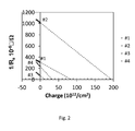
- Figure 2 depict as graph illustrating different results #1, #2, #3, #4 of a CJPV measurement on a p + n junction, wherein the slope of the fitted line corresponds or is related to the hole mobility in the shallow junction, while the x-axis intersection corresponds or is related to the active dose in the shallow junction.
- the table of Figure 3 shows the results for #1, #2, #3, #4 obtained with the CJPV method. It clearly shows higher activation for higher anneal temperature.
- the obtained mobility values are realistic and in agreement with literature (e.g. F. Severac et. al., Mater. Sci. Eng. B, 154-155 (2008), p. 225-228 ), for similarprocess conditions.
- Fig. 4 and Fig. 5 illustrate maps derived with methods according to the present disclosure, based on a silicon substrate which was exposed to a 0.2keV, B 1E14cm-2 doping level and a spike anneal at 950°C to produce a shallow junction.
- the map resolution for this example was 4x4 mm 2 .
- the above described calculation was applied to obtain ⁇ and D p for each pixel of the map.
- a contour map was calculated therefrom.
- Fig. 4 depicts a Mobility map (in cm 2 /Vs).
- Fig. 5 depicts an Active dose map (cm -2 ).
Landscapes
- Testing Or Measuring Of Semiconductors Or The Like (AREA)
- Physics & Mathematics (AREA)
- General Physics & Mathematics (AREA)
- Investigating Or Analyzing Materials By The Use Of Electric Means (AREA)
Abstract
a. providing a substrate comprising a shallow junction at a first main surface of the substrate, the shallow junction being formed substantially parallel to the first main;
b. providing a dielectric layer on top of the first main surface;
c. iterating a combination of the following iterated steps for at least two times:
- providing and determining a value of a respective charge on a predetermined area of the dielectric layer by means of a discharge means;
- measuring a corresponding junction photovoltage for the predetermined area;
d. deriving at least one of a measure of an average hole/electron mobility or a measure of a dose of active dopants for the predetermined area of the substrate, from the respective charges and the corresponding junction photo voltages; and associated computer program.
Description
- The present disclosure relates to the field of characterisation of shallow junctions for use in semiconductor devices.
- For the fabrication of shallow junctions for use in semiconductor devices such as for instance transistors, the activation anneal, which is typically applied after dopant implantation in a substrate, has often severe thermal budget limitations. As a consequence typically not all implanted dopants are activated.
- For process development of shallow junctions or passivation layers it is important and/or advantageous to know electrical characteristics of the junction.
- A straightforward method known in the art is the use of the so-called "four point probe" that measures the sheet resistance (Rs) of the upper junction layer, possibly in combination with secondary ion mass spectroscopy (SIMS), which then allows to determine the active concentration and dose. However the use of the "four point probe" method and SIMS relies on theoretical mobility values of the free carriers in the upper layer of interest. As the sheet resistance depends on the active dose and the average mobility of the free charge carriers in the layer of interest, the upper layer, measuring this mobility is important. This can be done by Hall measurements, but these are not straight forward and require special attention when contacting the sample. It is not an in-line metrology method and no mapping capabilities are possible.
- There exists no quick in-line metrology that can directly measure the active dose and average mobility of the free charge carriers in a shallow junction in-line.
- Thus, there exists a need for an in-line metrology method for determining active dose and the average mobility of the free charge carriers in-line, to gain more scientific insight in the activation process.
- It is an aim of the present disclosure to provide a method for characterization of shallow junctions for use in semiconductor devices in-line (i.e. during process flow). Characterisation may for instance be based on performing local measurements, and may include representing the measurements in a map format.
- A further aim of the present invention is to provide a method able to measure active dose and the average mobility of the free charge carriers directly and automatically.
- A further aim is to provide a method which can be used for selecting manufacturing processes and for manufacturing process optimization of shallow junctions, as well as for quality control in manufacturing.
- A further aim of the present invention is to avoid the high cost of characterisation by means of SIMS measurements as used in the prior art.
- These aims are achieved according to the disclosure with a method showing the technical characteristics of the first independent claim.
- It is another aim of the present disclosure to provide an associated computer program.
- According to a first aspect of the present invention, a method is disclosed for characterization of shallow junctions for use in semiconductor devices, the method comprising:
- a. providing a substrate comprising a shallow junction at a first main surface of the substrate, the shallow junction being formed substantially parallel to the first main surface;
- b. providing a dielectric layer on top of the first main surface;
- c. iterating a combination of the following iterated steps for at least two times:
- providing and determining a value of a respective charge on a predetermined area of the dielectric layer by means of a discharge means;
- measuring a corresponding junction photo voltage for the predetermined area;
- d. deriving at least one of a measure of an average hole/electron mobility (for instance the average hole/electron mobility) or a measure of a dose of active dopants (for instance the dose of active dopants) for the predetermined area of the substrate, from the respective charges and the corresponding junction photo voltages.
- This provides the advantage that in-line metrology can be performed, whereby active dose and the average mobility of the free charge carriers is determined directly and automatically. The dopant activation process in the shallow junction can thereby closely be monitored and analyzed.
- The substrate can be for instance a silicon, germanium or GaAs substrate. It can be any state of the art semiconductor substrate known to the skilled person on which a shallow junction is applied on a main surface.
- The predetermined area may comprise the full first main surface of the substrate.
- The shallow junction can be formed by ion implantation processes known to the skilled person. The junction can preferably have a thickness (or depth in another view) smaller than 100 nm, more preferably smaller than 75 nm, more preferably smaller than any value of 50, 40, 30, 20 ,10 nm.
- Providing and determining a value of a respective positive or negative charge on a predetermined area of the dielectric layer may embody a series of stepwise processes in which charges are added/removed for each iteration. The amount of removed or added charges between two iterations can for instance be substantially constant.
- The dielectric layer may be any state of the art dielectric layer known to be suitable to the skilled person. It may for instance be a SiO2 layer, which can for instance be deposited by a Plasma Enhanced CVD process (CVD). The thickness of the dielectric layer is preferably within the range of 10 to 100nm.
- According to preferred embodiments, the method further comprises removing or neutralizing the deposited charges from the predetermined area of the dielectric layer, after the series of iterations has ended (i.e. after iterating a combination of the iterated steps). Removing or neutralizing charges from the predetermined area of the dielectric layer can also be performed before starting the series of iterations (i.e. before iterating a combination of the iterated steps), if necessary.
- This provides the advantage that the method may be repeated under the same initial conditions.
- According to certain embodiments, possibly an initial corona charge deposition can be provided to compensate initial existing charge in the dielectric or charge contained in or at the interface traps. When the process is to be repeated under the same initial conditions, e.g. in order to estimate or reduce the systematic error of the method, the initial corona charge deposition can be repeated also.
- According to preferred embodiments, deriving at least one of a measure of an average hole/electron mobility or a measure of a dose of active dopants for the predetermined area comprises performing a linear fit.
- According to preferred embodiments, the linear fit is based on the
relation 1/Rs=µp.(q.Dp-Qc) for p+/n-Si and 1/Rs=µn.(q.Dn,+Qc) for n+/p-Si junctions, wherein Qc is the respective charge deposited on the dielectric layer, Rs is the sheet resistance of the upper junction layer, Dp/Dn is the authentic dose of holes/electrons before providing any charges, µp and µn are the average hole /electron mobility in the respective p+/ n+ layer of the shallow junction, and q is the unit of electrical charge. - According to preferred embodiments, the dielectric layer and the first main surface are in direct contact. The dielectric layer can be deposited on the first main surface.
- According to preferred embodiments, the respective charges are provided by corona charging.
- According to preferred embodiments, the shallow junction is a junction of the p+n type.
- According to preferred embodiments, the shallow junction is a junction of the n+p type.
- According to preferred embodiments, the respective charges are positive. They can for instance comprise positively charged ions.
- According to preferred embodiments, the respective charges are negative. They can for instance comprise negatively charged ion.
- In second aspect of the present invention, a method is disclosed for mapping characteristic information for a shallow junction on a substrate, comprising performing a method according to any of the embodiments of the first aspect, on at least two predetermined and disjoint areas.
- According to preferred embodiments, the method for mapping is being performed on a plurality of predetermined disjoint areas, and the union of the predetermined disjoint areas corresponds to the first main surface of the substrate.
- According to a third aspect of the present invention, a computer program is disclosed adapted for performing the steps of deriving at least one of a measure of an average hole/electron mobility or a measure of a dose of active dopants for a predetermined area of a substrate comprising a shallow junction, from respective charges and corresponding junction photo voltages as described in step (c) of the method according to the first aspect, when being run on a computer. The computer program may further be adapted to perform further steps of the method as explained for the first aspect. For instance, it may be adapted for performing a linear fit for deriving at least one of a measure of an average hole/electron mobility or a measure of a dose of active dopants for the predetermined area. Such a linear fit may be based on the
relation 1/Rs=µp.(q.Dp-Qc) or 1/Rs=µn.(q.Dn+Qc), as explained for the first aspect. - The disclosure will be further elucidated by means of the following description and the appended figures.
-
Figure 1 shows a typical setup for performing the method according to any of the embodiments of the present invention. -
Figure 2 illustrates an embodiment of the present invention based on a linear fitting of the measured data. -
Figure 3 is a table providing an overview of results obtained from the data shown inFigure 2 . -
Figure 4 illustrates a mobility map of a shallow junction measured with a method according to aspects of the present invention. -
Figure 5 illustrates an active dose map of a shallow junction measured with a method according to aspects of the present invention. - The present disclosure will be described with respect to particular embodiments and with reference to certain drawings but the disclosure is not limited thereto but only by the claims. The drawings described are only schematic and are non-limiting. In the drawings, the size of some of the elements may be exaggerated and not drawn on scale for illustrative purposes. The dimensions and the relative dimensions do not necessarily correspond to actual reductions to practice of the disclosure.
- Furthermore, the terms first, second, third and the like in the description and in the claims, are used for distinguishing between similar elements and not necessarily for describing a sequential or chronological order. The terms are interchangeable under appropriate circumstances and the embodiments of the disclosure can operate in other sequences than described or illustrated herein.
- Moreover, the terms top, bottom, over, under and the like in the description and the claims are used for descriptive purposes and not necessarily for describing relative positions. The terms so used are interchangeable under appropriate circumstances and the embodiments of the disclosure described herein can operate in other orientations than described or illustrated herein.
- Furthermore, the various embodiments, although referred to as "preferred" are to be construed as exemplary manners in which the disclosure may be implemented rather than as limiting the scope of the disclosure.
- The term "comprising", used in the claims, should not be interpreted as being restricted to the elements or steps listed thereafter; it does not exclude other elements or steps. It needs to be interpreted as specifying the presence of the stated features, integers, steps or components as referred to, but does not preclude the presence or addition of one or more other features, integers, steps or components, or groups thereof. Thus, the scope of the expression "a device comprising A and B" should not be limited to devices consisting only of components A and B, rather with respect to the present disclosure, the only enumerated components of the device are A and B, and further the claim should be interpreted as including equivalents of those components.
- In order to illustrate aspects of the present invention, a metrology tool of the Semilab WT-2000 type has been used, which comprises capabilities of corona charging and Junction Photo Voltage measurement (JPV). The functioning of this device is considered to known to the skilled person, and some relative aspects of its functioning has been described for instance in European Patent
EP1998184 B1 , which is hereby incorporated by reference. - The method comprises the combination of at least two measurement modules or devices, more specifically the combination of a first module able to apply a corona charge on a specific area on said interface surface and measuring the related surface voltage (referred to as Q-V module) and of a second module (referred to as the junction photovoltage module or JPV module), applying a laser or LED pulse at a fixed frequency leading to an illuminated spot within said specific area and subsequently measuring the induced photovoltage (V1) inside and (V2) outside respectively the illumination spot by means of two electrodes.
- The two electrodes measuring the voltages are preferably concentric or at least partly concentric. Alternatively the electrodes can be linear (in case the laser or LED spot is a concentric spot). The mobility is then derived from the sheet resistance (sheet resistance is inversely proportional to the mobility), that itself derives from the induced photovoltage (V1) and (V2) measured respectively inside and outside the illumination spot.
- By illuminated spot, it should be understood a small area defined by receiving a certain amount of energy from a laser or LED.
- By corona charge it should be understood as creating ionized molecules by corona discharge effect (by applying high voltage between a sharply curved electrode and the ground exceeding the Corona Inception Voltage of the charger assembly).
- The method preferably starts with the step of applying a corona charge on the dielectric layer to attract or repulse free charge carriers in the p+ or n+ top layer of the pn junction. Optionally, the corresponding surface potential is then measured preferably contactless using a Kelvin probe through a Q-V module, to check whether any corona charge leaked away. Then a measurement performed with the JPV module is used to determine the sheet resistance of the p+ or n+ layer of the shallow junction.
- The step of applying a corona charge is preferably performed over the entire substrate (wafer) by passing a metallic (e.g. tungsten) wire at a fixed potential (e.g. 10 kV) over the substrate surface. Alternatively and also preferred the Q-V corona charge is deposited locally by using a corona jet. In said corona jet, airflow blows out ions generated in an assembly consisting of a sharp needle centered in a tube which blows corona charge on the substrate surface locally on a (approximately 1cm2) predetermined area. The related surface voltage Vs (at least on said specific area) is preferably measured contactless using a Kelvin probe.
- A Kelvin probe can be defined as a vibrating electrode (~0.5cm2 area) positioned over the surface forming a capacitor. If the voltage applied to the electrode is equal to the surface voltage, the AC current flow has its minimum providing a way to measure the surface voltage in a non-contact way (the specific Kelvin probe was manufactured by Trek, Inc.).
- The step of measuring the sheet resistance of the free charge carriers in the p+ or n+ layer under the dielectric layer is performed using the JPV module. The JPV module is preferably used with a laser or LED pulse that creates electron-hole pairs in the underlying (e.g. Si or Ge) substrate. By applying a laser or LED pulse at a fixed frequency, an illuminated spot is created under the inner electrode, while the outer electrode remains in the dark region. Using an appropriate wavelength for the LED or laser light (e.g.470nm in case for Si), electron hole pairs are created in the illuminated region. On a p+n-type shallow junction , the internal electric field of the junction will move an excess amount of holes into the p+ layer near the interface surface of the dielectric layer and the (Si) substrate. Due to the charge gradient an electric field parallel to the interface surface will spread out the excess charges radially in parallel to the interface surface.
- By using two at least partly concentric electrodes whereby one electrode (R1) is situated within the illuminated spot and one electrode (R2) is situated outside the illuminated spot, the induced photovoltage V1 (originating from R1) and V2 (originating from R2) can be derived. The at least partly concentric electrodes can have a ring structure. The voltages V1 and V2 respectively are measured preferably contactless by the electrodes R1 and R2 respectively.
- Alternatively and also preferably, the electrodes can for instance be linear electrodes e.g. finger shaped electrodes.
- The measurement of the voltages V1 and V2 originating from the at least partly concentric electrodes can be performed in a contactless manner by capacitive coupling.
- The method which combines JPV measurements with corona voltage deposition can be applied on different wafer sites such that a sheet resistance mapping system is created. This new mapping method makes it possible to characterize the shallow junction on a substrate (e.g. Si wafer).
- According to preferred embodiments of the invention, the process of applying a corona charge is applied over the entire surface of the substrate by passing a metallic (e.g. tungsten) wire over the wafer, the wire is at a fixed voltage e.g. 10kV.
- By passing, it can be suggested a constant speed linear movement according to X and Y directions, obviously any other movement considered suitable to the skilled person can also be used. The speed of the displacement of the means creating the corona charge (a metallic wire or corona jet) will lead to the formation of the corona charges having a charge density.
- The speed determines the charge deposition and the speed can preferably vary between 0.01 and 20 cm/s.
- Alternatively, although less preferred because of current practical limitations, the step of applying a corona is applied locally on a dedicated area by using a corona jet, which blows corona charge on the wafer surface locally on an about 2 cm2 area.
- According to preferred embodiments of the invention, the step of measuring the surface voltage Vs at least locally on a dedicated area is performed using a Kelvin probe. Preferably the measurement is performed contactless.
- According to preferred embodiments of the invention, the step of creating an excess amount of free charges in the shallow junction (holes for p+-type silicon, electrons for n+-type silicon) at least locally on a dedicated area onto the substrate is performed using a laser or LED pulse which creates electron hole pairs in the substrate underneath the at least one dielectric layer such that an excess amount of the free charges is created locally in the upper layer of the shallow junction near the interface formed by the surface dielectric layer and semiconductor.
- According to preferred embodiments of the invention, the step of measuring the photovoltage inside and outside the illuminated spot by means of two at least partly concentric electrodes is performed using the Junction Photo Voltage module. The basis of the JPV measurement is to use photo excitation of charge carriers and to monitor in a spatially resolved manner the JPV signals inside and outside the illumination spot.
- According to preferred embodiments of the invention, the substrate is a flat substrate such as e.g. a silicon (Si) or germanium (Ge) wafer. The substrate can also be a SOI (Silicon-On-Insulator) or a GOI (Germanium-On-Insulator) substrate which is basically a silicon (germanium) wafer with a thin layer of oxide (e.g. Si02) buried on it as dielectric layer. The substrate can be cleaned prior to the step of depositing a dielectric layer to remove contaminants. Preferably the substrate can be doped and annealed to obtain e.g. a p+n-doped or n+p- shallow junction substrate.
- According to another preferred embodiment of the invention, the at least one dielectric layer is a single dielectric layer or a combination of dielectric layers (for example a "dual dielectricum"). Preferred examples of dielectric materials used as for dielectric layers are materials such as SiO2 layers, SiN, SiON , HfO2 or other metallic/rare-earth oxides such as ZrO2, Al2O3, La2O3, Pr2O3, Ta2O5,... and also the related silicates of these metals/rare-earth elements. The thickness of the dielectric layer can be for instance within the range of 10 to 100nm.
- According to preferred embodiments of the invention, the process of depositing at least one dielectric layer is performed using deposition techniques such as for instance Chemical Vapor Deposition (CVD), Plasma Enhanced CVD (PECVD), Metal Organic Chemical Vapor Deposition (MOCVD), Atomic Layer Deposition (ALD).
-
Figure 1 illustrates a method according to a preferred embodiment of the present invention. An n-type silicon substrate 1 is provided. After shallow junction formation by ion implantation, defining a p+n junction 2 at or in a front surface of the substrate, an electricalinsulating dielectric 3 is deposited. Here, a CVD oxide with a thickness of 50 nm is deposited at 400 °C. A shallow p+ n junction is used, made by B-implant in n-type silicon at 0.2keV. - A series of
corona charge depositions 4 was performed, each followed by a junction photovoltage (JPV) measurement. This type of measurement is further denoted as CJPV. The JPV delivers the sheet resistance Rs of the p+ layer below the dielectric layer, the oxide (Fig.1 ). The oxide prevents that any corona charge leaks away. It influences the amount of free carriers in the p+ layer by induction. A positive corona charge will repulse the holes in the p+ layer resulting in a higher Rs. A negative corona charge will attract an equal amount of positively chargedholes 5, decreasing the Rs. 1/Rs can be expressed as :
in which µ is the average hole mobility in the p+ layer, Dp is the original (before corona charging) dose of holes and q is the unit charge. Dp is to good approximation equal to the dose of active boron dopants. Qc is the corona charge deposited on the oxide which can be positive as well as negative. A linear relationship exists between 1/Rs and QC for which the slope represents the average hole mobility while the x-axis intersection represents qDp. So if an amount of corona charge Qc equal to qDp could be deposited, then no conductance would be detected anymore. In practice this is not possible as the amount of corona charge would be so high that the corona charge would leak away by tunneling or oxide break down. This means an extrapolation from the data points is needed as shown inFig.2 . Similarly this technique can be applied on n+p, for instance comprising arsenic or phosphor implanted in p-type Silicon substrate. Also junctions on other substrates as for instance Ge and GaAs substrates can be measured this way. -
Figure 2 depict as graph illustratingdifferent results # 1, #2, #3, #4 of a CJPV measurement on a p+n junction, wherein the slope of the fitted line corresponds or is related to the hole mobility in the shallow junction, while the x-axis intersection corresponds or is related to the active dose in the shallow junction. - The table of
Figure 3 shows the results for #1, #2, #3, #4 obtained with the CJPV method. It clearly shows higher activation for higher anneal temperature. The obtained mobility values are realistic and in agreement with literature (e.g. F. Severac et. al., Mater. Sci. Eng. B, 154-155 (2008), p. 225-228), for similarprocess conditions. - It will be appreciated that this combination of corona charge and JPV can be implemented as a fully automated, fast, in-line metrology. The automatization also allows mapping capability.
-
Fig. 4 andFig. 5 illustrate maps derived with methods according to the present disclosure, based on a silicon substrate which was exposed to a 0.2keV, B 1E14cm-2 doping level and a spike anneal at 950°C to produce a shallow junction. The map resolution for this example was 4x4 mm2. The above described calculation was applied to obtain µ and Dp for each pixel of the map. A contour map was calculated therefrom.Fig. 4 depicts a Mobility map (in cm2/Vs).Fig. 5 depicts an Active dose map (cm-2).
Claims (13)
- Method for characterisation of shallow junctions for use in semiconductor devices, the method comprising:a. providing a substrate comprising a shallow junction at a first main surface of said substrate, said shallow junction being formed substantially parallel to said first main;b. providing a dielectric layer on top of said first main surface;c. iterating a combination of the following iterated steps for at least two times:- providing and determining a value of a respective charge on a predetermined area of said dielectric layer by means of a discharge means;- measuring a corresponding junction photovoltage for said predetermined area;d. deriving at least one of a measure of an average hole/electron mobility or a measure of a dose of active dopants for said predetermined area of said substrate, from said respective charges and said corresponding junction photo voltages.
- Method according to claim 1, further comprising removing or neutralizing the deposited charges from the predetermined area of the dielectric layer, before iterating a combination of said iterated steps.
- Method according to claim 1 or 2, wherein said deriving at least one of a measure of an average hole/electron mobility or a measure of a dose of active dopants for said predetermined area comprises performing a linear fit.
- Method according to claim 3, wherein said linear fit is based on the relation 1/Rs=µp.(q.Dp-Qc) or 1/Rs=µn.(q.Dn+Qc), wherein Qc is the respective charge deposited on said dielectric layer, Rs is the sheet resistance of the upper junction layer, Dp / Dn is the authentic dose of holes/electrons before providing any charges, µp/µn is the average hole/electron mobility in the p+ / n+ upper layer of the shallow junction, and q is the unit of electrical charge.
- Method according to any of the previous claims, wherein said dielectric layer and said first main surface are in direct contact.
- Method according to any of the previous claims, wherein said respective charges are provided by corona charging.
- A method according to any of the previous claims, wherein said shallow junction is a junction of the p+n type.
- A method according to any of the previous claims, wherein said shallow junction is a junction of the n+p type.
- A method according to any of the previous claims, wherein said respective charges are positive.
- A method according to any of the previous claims 1 to 8, wherein said respective charges are negative.
- Method for mapping characteristic information for a shallow junction on a substrate, comprising performing a method according to any of claims 1 to 10 on at least two predetermined and disjoint areas.
- Method according to claim 11, being performed on a plurality of predetermined disjoint areas, wherein the union of said predetermined disjoint areas corresponds to said first main surface of said substrate.
- A computer program adapted for performing the steps of deriving at least one of a measure of an average hole/electron mobility or a measure of a dose of active dopants for a predetermined area of a substrate comprising a shallow junction, from respective charges and corresponding junction photo voltages as used and/or derived in step (c) of claim 1, when run on a computer.
Priority Applications (4)
| Application Number | Priority Date | Filing Date | Title |
|---|---|---|---|
| EP13151644.5A EP2757579B1 (en) | 2013-01-17 | 2013-01-17 | Method for characterisation of shallow junctions for use in semiconductor devices |
| JP2013269213A JP6208006B2 (en) | 2013-01-17 | 2013-12-26 | Evaluation method for shallow junctions used in semiconductor devices |
| TW103101551A TWI601213B (en) | 2013-01-17 | 2014-01-16 | Method for forming shallow junctions for semiconductor devices |
| US14/157,373 US9472474B2 (en) | 2013-01-17 | 2014-01-16 | Methods for characterizing shallow semiconductor junctions |
Applications Claiming Priority (1)
| Application Number | Priority Date | Filing Date | Title |
|---|---|---|---|
| EP13151644.5A EP2757579B1 (en) | 2013-01-17 | 2013-01-17 | Method for characterisation of shallow junctions for use in semiconductor devices |
Publications (2)
| Publication Number | Publication Date |
|---|---|
| EP2757579A1 true EP2757579A1 (en) | 2014-07-23 |
| EP2757579B1 EP2757579B1 (en) | 2019-06-19 |
Family
ID=47664140
Family Applications (1)
| Application Number | Title | Priority Date | Filing Date |
|---|---|---|---|
| EP13151644.5A Active EP2757579B1 (en) | 2013-01-17 | 2013-01-17 | Method for characterisation of shallow junctions for use in semiconductor devices |
Country Status (4)
| Country | Link |
|---|---|
| US (1) | US9472474B2 (en) |
| EP (1) | EP2757579B1 (en) |
| JP (1) | JP6208006B2 (en) |
| TW (1) | TWI601213B (en) |
Families Citing this family (2)
| Publication number | Priority date | Publication date | Assignee | Title |
|---|---|---|---|---|
| CN107706122B (en) * | 2017-10-18 | 2020-06-26 | 武汉新芯集成电路制造有限公司 | A kind of detection method of annealing process |
| JP6451881B1 (en) * | 2018-01-24 | 2019-01-16 | 株式会社Sumco | Silicon layer evaluation method and silicon epitaxial wafer manufacturing method |
Citations (3)
| Publication number | Priority date | Publication date | Assignee | Title |
|---|---|---|---|---|
| US4638341A (en) * | 1984-09-06 | 1987-01-20 | Honeywell Inc. | Gated transmission line model structure for characterization of field-effect transistors |
| EP1998184A1 (en) * | 2007-05-29 | 2008-12-03 | Interuniversitair Microelektronica Centrum (IMEC) | Mobility measurements of inversion charge carriers |
| US7521946B1 (en) * | 2005-04-06 | 2009-04-21 | Kla-Tencor Technologies Corporation | Electrical measurements on semiconductors using corona and microwave techniques |
Family Cites Families (10)
| Publication number | Priority date | Publication date | Assignee | Title |
|---|---|---|---|---|
| US4812756A (en) | 1987-08-26 | 1989-03-14 | International Business Machines Corporation | Contactless technique for semicondutor wafer testing |
| US5216362A (en) | 1991-10-08 | 1993-06-01 | International Business Machines Corporation | Contactless technique for measuring epitaxial dopant concentration profiles in semiconductor wafers |
| US5519334A (en) * | 1994-09-29 | 1996-05-21 | Advanced Micro Devices, Inc. | System and method for measuring charge traps within a dielectric layer formed on a semiconductor wafer |
| US6104206A (en) | 1997-08-05 | 2000-08-15 | Verkuil; Roger L. | Product wafer junction leakage measurement using corona and a kelvin probe |
| US5834941A (en) | 1997-08-11 | 1998-11-10 | Keithley Instruments, Inc. | Mobile charge measurement using corona charge and ultraviolet light |
| US6255128B1 (en) * | 1998-08-06 | 2001-07-03 | Lucent Technologies Inc. | Non-contact method for determining the presence of a contaminant in a semiconductor device |
| JP3450770B2 (en) * | 1999-11-29 | 2003-09-29 | 松下電器産業株式会社 | Method for manufacturing semiconductor device |
| US7019513B1 (en) * | 2005-01-19 | 2006-03-28 | Vladimir Faifer | Non-contact method and apparatus for measurement of sheet resistance and leakage current of p-n junctions |
| US7696021B2 (en) * | 2005-11-14 | 2010-04-13 | Texas Instruments Incorporated | Semiconductor device manufactured using a non-contact implant metrology |
| US20110301892A1 (en) * | 2010-06-03 | 2011-12-08 | Emil Kamieniecki | System and method for characterizing the electrical properties of a semiconductor sample |
-
2013
- 2013-01-17 EP EP13151644.5A patent/EP2757579B1/en active Active
- 2013-12-26 JP JP2013269213A patent/JP6208006B2/en active Active
-
2014
- 2014-01-16 TW TW103101551A patent/TWI601213B/en active
- 2014-01-16 US US14/157,373 patent/US9472474B2/en active Active
Patent Citations (3)
| Publication number | Priority date | Publication date | Assignee | Title |
|---|---|---|---|---|
| US4638341A (en) * | 1984-09-06 | 1987-01-20 | Honeywell Inc. | Gated transmission line model structure for characterization of field-effect transistors |
| US7521946B1 (en) * | 2005-04-06 | 2009-04-21 | Kla-Tencor Technologies Corporation | Electrical measurements on semiconductors using corona and microwave techniques |
| EP1998184A1 (en) * | 2007-05-29 | 2008-12-03 | Interuniversitair Microelektronica Centrum (IMEC) | Mobility measurements of inversion charge carriers |
Non-Patent Citations (2)
| Title |
|---|
| MICHAEL CURRENT ET AL: "Dopant Activation and Leakage Current Aspects of SDE/Halo CMOS Junctions Measured with Non-contact Junction Photo-Voltage Methods", JUNCTION TECHNOLOGY, 2007 INTERNATIONAL WORKSHOP ON, IEEE, PI, June 2007 (2007-06-01), pages 43 - 46, XP031120215, ISBN: 978-1-4244-1103-0 * |
| STEVEN M BAIER ET AL: "FET Characterization Using Gated-TLM Structure", IEEE TRANSACTIONS ON ELECTRON DEVICES, IEEE SERVICE CENTER, PISACATAWAY, NJ, US, vol. ED-32, no. 12, December 1985 (1985-12-01), pages 2824 - 2829, XP001292553, ISSN: 0018-9383 * |
Also Published As
| Publication number | Publication date |
|---|---|
| JP6208006B2 (en) | 2017-10-04 |
| EP2757579B1 (en) | 2019-06-19 |
| TWI601213B (en) | 2017-10-01 |
| US20140197862A1 (en) | 2014-07-17 |
| US9472474B2 (en) | 2016-10-18 |
| TW201436053A (en) | 2014-09-16 |
| JP2014146790A (en) | 2014-08-14 |
Similar Documents
| Publication | Publication Date | Title |
|---|---|---|
| Pellegrini et al. | First double-sided 3-D detectors fabricated at CNM-IMB | |
| Wilson et al. | Recent Advancement in Charge-and Photo-Assisted Non-Contact Electrical Characterization of SiC, GaN, and AlGaN/GaN HEMT | |
| JP6272741B2 (en) | Extraction method of recombination characteristics on metallized semiconductor surface | |
| EP1998184B1 (en) | Mobility measurements of inversion charge carriers | |
| US8004290B1 (en) | Method and apparatus for determining dielectric layer properties | |
| Fırat et al. | Local enhancement of dopant diffusion from polycrystalline silicon passivating contacts | |
| CN104303280B (en) | Evaluation method of semiconductor substrate, semiconductor substrate for evaluation, semiconductor device | |
| EP2757579B1 (en) | Method for characterisation of shallow junctions for use in semiconductor devices | |
| JP2011100909A (en) | Method for evaluating semiconductor substrate and method for manufacturing semiconductor device | |
| Xiao et al. | Locating the electrical junctions in Cu (In, Ga) Se2 and Cu2ZnSnSe4 solar cells by scanning capacitance spectroscopy | |
| Pushkarev et al. | Optimizing non-contact doping and electrical defect metrology for production of SiC epitaxial wafers | |
| Jatzkowski et al. | Novel techniques for dopant contrast analysis on real IC structures | |
| US7696021B2 (en) | Semiconductor device manufactured using a non-contact implant metrology | |
| Hameiri et al. | The impact of surface damage region and edge recombination on the effective lifetime of silicon wafers at low illumination conditions | |
| WO2024196595A1 (en) | Semiconductor doping characterization method using photoneutralization time constant of corona surface charge | |
| Nanver et al. | Test structures without metal contacts for DC measurement of 2D-materials deposited on silicon | |
| Savtchouk et al. | Accurate Doping Density Determination in SiC with Constant Surface Potential Corona Charging; Industry Ready Alternative to Hg-CV | |
| Verma et al. | Multiple contacts investigation of single silicon nanowires with the active voltage contrast scanning electron microscopy technique | |
| EP1610373A2 (en) | Method and apparatus for determining generation lifetime of product semiconductor wafers | |
| US20060208256A1 (en) | Self-calibration in non-contact surface photovoltage measurement of depletion capacitance and dopant concentration | |
| CN119480661B (en) | Detection method | |
| JP2021036558A (en) | Evaluation method for semiconductor samples | |
| Faifer et al. | Junction photovoltage (JPV) techniques for ultra-shallow junction characterization | |
| Golshani et al. | Manufacturing uniform field silicon drift detector using double boron layer | |
| Marinskiy et al. | Kelvin Force Microscopy and corona charging for semiconductor material and device characterization |
Legal Events
| Date | Code | Title | Description |
|---|---|---|---|
| PUAI | Public reference made under article 153(3) epc to a published international application that has entered the european phase |
Free format text: ORIGINAL CODE: 0009012 |
|
| 17P | Request for examination filed |
Effective date: 20130117 |
|
| AK | Designated contracting states |
Kind code of ref document: A1 Designated state(s): AL AT BE BG CH CY CZ DE DK EE ES FI FR GB GR HR HU IE IS IT LI LT LU LV MC MK MT NL NO PL PT RO RS SE SI SK SM TR |
|
| AX | Request for extension of the european patent |
Extension state: BA ME |
|
| R17P | Request for examination filed (corrected) |
Effective date: 20150123 |
|
| RBV | Designated contracting states (corrected) |
Designated state(s): AL AT BE BG CH CY CZ DE DK EE ES FI FR GB GR HR HU IE IS IT LI LT LU LV MC MK MT NL NO PL PT RO RS SE SI SK SM TR |
|
| STAA | Information on the status of an ep patent application or granted ep patent |
Free format text: STATUS: EXAMINATION IS IN PROGRESS |
|
| 17Q | First examination report despatched |
Effective date: 20170213 |
|
| RAP1 | Party data changed (applicant data changed or rights of an application transferred) |
Owner name: IMEC VZW |
|
| RIC1 | Information provided on ipc code assigned before grant |
Ipc: H01L 21/66 20060101AFI20181127BHEP Ipc: G01R 31/26 20140101ALN20181127BHEP |
|
| GRAP | Despatch of communication of intention to grant a patent |
Free format text: ORIGINAL CODE: EPIDOSNIGR1 |
|
| STAA | Information on the status of an ep patent application or granted ep patent |
Free format text: STATUS: GRANT OF PATENT IS INTENDED |
|
| RIC1 | Information provided on ipc code assigned before grant |
Ipc: H01L 21/66 20060101AFI20181217BHEP Ipc: G01R 31/26 20140101ALN20181217BHEP |
|
| INTG | Intention to grant announced |
Effective date: 20190123 |
|
| GRAS | Grant fee paid |
Free format text: ORIGINAL CODE: EPIDOSNIGR3 |
|
| GRAA | (expected) grant |
Free format text: ORIGINAL CODE: 0009210 |
|
| STAA | Information on the status of an ep patent application or granted ep patent |
Free format text: STATUS: THE PATENT HAS BEEN GRANTED |
|
| AK | Designated contracting states |
Kind code of ref document: B1 Designated state(s): AL AT BE BG CH CY CZ DE DK EE ES FI FR GB GR HR HU IE IS IT LI LT LU LV MC MK MT NL NO PL PT RO RS SE SI SK SM TR |
|
| REG | Reference to a national code |
Ref country code: GB Ref legal event code: FG4D |
|
| REG | Reference to a national code |
Ref country code: CH Ref legal event code: EP |
|
| REG | Reference to a national code |
Ref country code: IE Ref legal event code: FG4D |
|
| REG | Reference to a national code |
Ref country code: DE Ref legal event code: R096 Ref document number: 602013056705 Country of ref document: DE |
|
| REG | Reference to a national code |
Ref country code: AT Ref legal event code: REF Ref document number: 1146572 Country of ref document: AT Kind code of ref document: T Effective date: 20190715 |
|
| REG | Reference to a national code |
Ref country code: NL Ref legal event code: MP Effective date: 20190619 |
|
| PG25 | Lapsed in a contracting state [announced via postgrant information from national office to epo] |
Ref country code: LT Free format text: LAPSE BECAUSE OF FAILURE TO SUBMIT A TRANSLATION OF THE DESCRIPTION OR TO PAY THE FEE WITHIN THE PRESCRIBED TIME-LIMIT Effective date: 20190619 Ref country code: HR Free format text: LAPSE BECAUSE OF FAILURE TO SUBMIT A TRANSLATION OF THE DESCRIPTION OR TO PAY THE FEE WITHIN THE PRESCRIBED TIME-LIMIT Effective date: 20190619 Ref country code: FI Free format text: LAPSE BECAUSE OF FAILURE TO SUBMIT A TRANSLATION OF THE DESCRIPTION OR TO PAY THE FEE WITHIN THE PRESCRIBED TIME-LIMIT Effective date: 20190619 Ref country code: SE Free format text: LAPSE BECAUSE OF FAILURE TO SUBMIT A TRANSLATION OF THE DESCRIPTION OR TO PAY THE FEE WITHIN THE PRESCRIBED TIME-LIMIT Effective date: 20190619 Ref country code: AL Free format text: LAPSE BECAUSE OF FAILURE TO SUBMIT A TRANSLATION OF THE DESCRIPTION OR TO PAY THE FEE WITHIN THE PRESCRIBED TIME-LIMIT Effective date: 20190619 Ref country code: NO Free format text: LAPSE BECAUSE OF FAILURE TO SUBMIT A TRANSLATION OF THE DESCRIPTION OR TO PAY THE FEE WITHIN THE PRESCRIBED TIME-LIMIT Effective date: 20190919 |
|
| REG | Reference to a national code |
Ref country code: LT Ref legal event code: MG4D |
|
| PG25 | Lapsed in a contracting state [announced via postgrant information from national office to epo] |
Ref country code: GR Free format text: LAPSE BECAUSE OF FAILURE TO SUBMIT A TRANSLATION OF THE DESCRIPTION OR TO PAY THE FEE WITHIN THE PRESCRIBED TIME-LIMIT Effective date: 20190920 Ref country code: RS Free format text: LAPSE BECAUSE OF FAILURE TO SUBMIT A TRANSLATION OF THE DESCRIPTION OR TO PAY THE FEE WITHIN THE PRESCRIBED TIME-LIMIT Effective date: 20190619 Ref country code: BG Free format text: LAPSE BECAUSE OF FAILURE TO SUBMIT A TRANSLATION OF THE DESCRIPTION OR TO PAY THE FEE WITHIN THE PRESCRIBED TIME-LIMIT Effective date: 20190919 Ref country code: LV Free format text: LAPSE BECAUSE OF FAILURE TO SUBMIT A TRANSLATION OF THE DESCRIPTION OR TO PAY THE FEE WITHIN THE PRESCRIBED TIME-LIMIT Effective date: 20190619 |
|
| REG | Reference to a national code |
Ref country code: AT Ref legal event code: MK05 Ref document number: 1146572 Country of ref document: AT Kind code of ref document: T Effective date: 20190619 |
|
| PG25 | Lapsed in a contracting state [announced via postgrant information from national office to epo] |
Ref country code: PT Free format text: LAPSE BECAUSE OF FAILURE TO SUBMIT A TRANSLATION OF THE DESCRIPTION OR TO PAY THE FEE WITHIN THE PRESCRIBED TIME-LIMIT Effective date: 20191021 Ref country code: SK Free format text: LAPSE BECAUSE OF FAILURE TO SUBMIT A TRANSLATION OF THE DESCRIPTION OR TO PAY THE FEE WITHIN THE PRESCRIBED TIME-LIMIT Effective date: 20190619 Ref country code: EE Free format text: LAPSE BECAUSE OF FAILURE TO SUBMIT A TRANSLATION OF THE DESCRIPTION OR TO PAY THE FEE WITHIN THE PRESCRIBED TIME-LIMIT Effective date: 20190619 Ref country code: AT Free format text: LAPSE BECAUSE OF FAILURE TO SUBMIT A TRANSLATION OF THE DESCRIPTION OR TO PAY THE FEE WITHIN THE PRESCRIBED TIME-LIMIT Effective date: 20190619 Ref country code: NL Free format text: LAPSE BECAUSE OF FAILURE TO SUBMIT A TRANSLATION OF THE DESCRIPTION OR TO PAY THE FEE WITHIN THE PRESCRIBED TIME-LIMIT Effective date: 20190619 Ref country code: CZ Free format text: LAPSE BECAUSE OF FAILURE TO SUBMIT A TRANSLATION OF THE DESCRIPTION OR TO PAY THE FEE WITHIN THE PRESCRIBED TIME-LIMIT Effective date: 20190619 Ref country code: RO Free format text: LAPSE BECAUSE OF FAILURE TO SUBMIT A TRANSLATION OF THE DESCRIPTION OR TO PAY THE FEE WITHIN THE PRESCRIBED TIME-LIMIT Effective date: 20190619 |
|
| PG25 | Lapsed in a contracting state [announced via postgrant information from national office to epo] |
Ref country code: SM Free format text: LAPSE BECAUSE OF FAILURE TO SUBMIT A TRANSLATION OF THE DESCRIPTION OR TO PAY THE FEE WITHIN THE PRESCRIBED TIME-LIMIT Effective date: 20190619 Ref country code: IS Free format text: LAPSE BECAUSE OF FAILURE TO SUBMIT A TRANSLATION OF THE DESCRIPTION OR TO PAY THE FEE WITHIN THE PRESCRIBED TIME-LIMIT Effective date: 20191019 Ref country code: ES Free format text: LAPSE BECAUSE OF FAILURE TO SUBMIT A TRANSLATION OF THE DESCRIPTION OR TO PAY THE FEE WITHIN THE PRESCRIBED TIME-LIMIT Effective date: 20190619 Ref country code: IT Free format text: LAPSE BECAUSE OF FAILURE TO SUBMIT A TRANSLATION OF THE DESCRIPTION OR TO PAY THE FEE WITHIN THE PRESCRIBED TIME-LIMIT Effective date: 20190619 |
|
| PG25 | Lapsed in a contracting state [announced via postgrant information from national office to epo] |
Ref country code: TR Free format text: LAPSE BECAUSE OF FAILURE TO SUBMIT A TRANSLATION OF THE DESCRIPTION OR TO PAY THE FEE WITHIN THE PRESCRIBED TIME-LIMIT Effective date: 20190619 |
|
| PG25 | Lapsed in a contracting state [announced via postgrant information from national office to epo] |
Ref country code: PL Free format text: LAPSE BECAUSE OF FAILURE TO SUBMIT A TRANSLATION OF THE DESCRIPTION OR TO PAY THE FEE WITHIN THE PRESCRIBED TIME-LIMIT Effective date: 20190619 Ref country code: DK Free format text: LAPSE BECAUSE OF FAILURE TO SUBMIT A TRANSLATION OF THE DESCRIPTION OR TO PAY THE FEE WITHIN THE PRESCRIBED TIME-LIMIT Effective date: 20190619 |
|
| PG25 | Lapsed in a contracting state [announced via postgrant information from national office to epo] |
Ref country code: IS Free format text: LAPSE BECAUSE OF FAILURE TO SUBMIT A TRANSLATION OF THE DESCRIPTION OR TO PAY THE FEE WITHIN THE PRESCRIBED TIME-LIMIT Effective date: 20200224 |
|
| REG | Reference to a national code |
Ref country code: DE Ref legal event code: R097 Ref document number: 602013056705 Country of ref document: DE |
|
| PLBE | No opposition filed within time limit |
Free format text: ORIGINAL CODE: 0009261 |
|
| STAA | Information on the status of an ep patent application or granted ep patent |
Free format text: STATUS: NO OPPOSITION FILED WITHIN TIME LIMIT |
|
| PG2D | Information on lapse in contracting state deleted |
Ref country code: IS |
|
| 26N | No opposition filed |
Effective date: 20200603 |
|
| PG25 | Lapsed in a contracting state [announced via postgrant information from national office to epo] |
Ref country code: SI Free format text: LAPSE BECAUSE OF FAILURE TO SUBMIT A TRANSLATION OF THE DESCRIPTION OR TO PAY THE FEE WITHIN THE PRESCRIBED TIME-LIMIT Effective date: 20190619 Ref country code: MC Free format text: LAPSE BECAUSE OF FAILURE TO SUBMIT A TRANSLATION OF THE DESCRIPTION OR TO PAY THE FEE WITHIN THE PRESCRIBED TIME-LIMIT Effective date: 20190619 |
|
| REG | Reference to a national code |
Ref country code: CH Ref legal event code: PL |
|
| GBPC | Gb: european patent ceased through non-payment of renewal fee |
Effective date: 20200117 |
|
| REG | Reference to a national code |
Ref country code: BE Ref legal event code: MM Effective date: 20200131 |
|
| PG25 | Lapsed in a contracting state [announced via postgrant information from national office to epo] |
Ref country code: LU Free format text: LAPSE BECAUSE OF NON-PAYMENT OF DUE FEES Effective date: 20200117 Ref country code: GB Free format text: LAPSE BECAUSE OF NON-PAYMENT OF DUE FEES Effective date: 20200117 |
|
| PG25 | Lapsed in a contracting state [announced via postgrant information from national office to epo] |
Ref country code: CH Free format text: LAPSE BECAUSE OF NON-PAYMENT OF DUE FEES Effective date: 20200131 Ref country code: LI Free format text: LAPSE BECAUSE OF NON-PAYMENT OF DUE FEES Effective date: 20200131 Ref country code: BE Free format text: LAPSE BECAUSE OF NON-PAYMENT OF DUE FEES Effective date: 20200131 |
|
| PG25 | Lapsed in a contracting state [announced via postgrant information from national office to epo] |
Ref country code: IE Free format text: LAPSE BECAUSE OF NON-PAYMENT OF DUE FEES Effective date: 20200117 |
|
| PG25 | Lapsed in a contracting state [announced via postgrant information from national office to epo] |
Ref country code: MT Free format text: LAPSE BECAUSE OF FAILURE TO SUBMIT A TRANSLATION OF THE DESCRIPTION OR TO PAY THE FEE WITHIN THE PRESCRIBED TIME-LIMIT Effective date: 20190619 Ref country code: CY Free format text: LAPSE BECAUSE OF FAILURE TO SUBMIT A TRANSLATION OF THE DESCRIPTION OR TO PAY THE FEE WITHIN THE PRESCRIBED TIME-LIMIT Effective date: 20190619 |
|
| PG25 | Lapsed in a contracting state [announced via postgrant information from national office to epo] |
Ref country code: MK Free format text: LAPSE BECAUSE OF FAILURE TO SUBMIT A TRANSLATION OF THE DESCRIPTION OR TO PAY THE FEE WITHIN THE PRESCRIBED TIME-LIMIT Effective date: 20190619 |
|
| P01 | Opt-out of the competence of the unified patent court (upc) registered |
Effective date: 20230513 |
|
| REG | Reference to a national code |
Ref country code: DE Ref legal event code: R079 Ref document number: 602013056705 Country of ref document: DE Free format text: PREVIOUS MAIN CLASS: H01L0021660000 Ipc: H10P0074000000 |
|
| PGFP | Annual fee paid to national office [announced via postgrant information from national office to epo] |
Ref country code: FR Payment date: 20251218 Year of fee payment: 14 |
|
| PGFP | Annual fee paid to national office [announced via postgrant information from national office to epo] |
Ref country code: DE Payment date: 20251217 Year of fee payment: 14 |