EP2757561B1 - Write pole box shield - Google Patents
Write pole box shield Download PDFInfo
- Publication number
- EP2757561B1 EP2757561B1 EP14151657.5A EP14151657A EP2757561B1 EP 2757561 B1 EP2757561 B1 EP 2757561B1 EP 14151657 A EP14151657 A EP 14151657A EP 2757561 B1 EP2757561 B1 EP 2757561B1
- Authority
- EP
- European Patent Office
- Prior art keywords
- magnetic
- gap
- layer
- write pole
- data writer
- Prior art date
- Legal status (The legal status is an assumption and is not a legal conclusion. Google has not performed a legal analysis and makes no representation as to the accuracy of the status listed.)
- Not-in-force
Links
Images

Classifications
-
- G—PHYSICS
- G11—INFORMATION STORAGE
- G11B—INFORMATION STORAGE BASED ON RELATIVE MOVEMENT BETWEEN RECORD CARRIER AND TRANSDUCER
- G11B5/00—Recording by magnetisation or demagnetisation of a record carrier; Reproducing by magnetic means; Record carriers therefor
- G11B5/10—Structure or manufacture of housings or shields for heads
- G11B5/11—Shielding of head against electric or magnetic fields
- G11B5/115—Shielding devices arranged between heads or windings
-
- G—PHYSICS
- G11—INFORMATION STORAGE
- G11B—INFORMATION STORAGE BASED ON RELATIVE MOVEMENT BETWEEN RECORD CARRIER AND TRANSDUCER
- G11B5/00—Recording by magnetisation or demagnetisation of a record carrier; Reproducing by magnetic means; Record carriers therefor
- G11B5/127—Structure or manufacture of heads, e.g. inductive
- G11B5/1278—Structure or manufacture of heads, e.g. inductive specially adapted for magnetisations perpendicular to the surface of the record carrier
-
- G—PHYSICS
- G11—INFORMATION STORAGE
- G11B—INFORMATION STORAGE BASED ON RELATIVE MOVEMENT BETWEEN RECORD CARRIER AND TRANSDUCER
- G11B5/00—Recording by magnetisation or demagnetisation of a record carrier; Reproducing by magnetic means; Record carriers therefor
- G11B5/127—Structure or manufacture of heads, e.g. inductive
- G11B5/187—Structure or manufacture of the surface of the head in physical contact with, or immediately adjacent to the recording medium; Pole pieces; Gap features
- G11B5/23—Gap features
-
- G—PHYSICS
- G11—INFORMATION STORAGE
- G11B—INFORMATION STORAGE BASED ON RELATIVE MOVEMENT BETWEEN RECORD CARRIER AND TRANSDUCER
- G11B5/00—Recording by magnetisation or demagnetisation of a record carrier; Reproducing by magnetic means; Record carriers therefor
- G11B5/127—Structure or manufacture of heads, e.g. inductive
- G11B5/31—Structure or manufacture of heads, e.g. inductive using thin films
- G11B5/3109—Details
- G11B5/3116—Shaping of layers, poles or gaps for improving the form of the electrical signal transduced, e.g. for shielding, contour effect, equalizing, side flux fringing, cross talk reduction between heads or between heads and information tracks
-
- G—PHYSICS
- G11—INFORMATION STORAGE
- G11B—INFORMATION STORAGE BASED ON RELATIVE MOVEMENT BETWEEN RECORD CARRIER AND TRANSDUCER
- G11B5/00—Recording by magnetisation or demagnetisation of a record carrier; Reproducing by magnetic means; Record carriers therefor
- G11B5/127—Structure or manufacture of heads, e.g. inductive
- G11B5/31—Structure or manufacture of heads, e.g. inductive using thin films
- G11B5/3109—Details
- G11B5/313—Disposition of layers
- G11B5/3143—Disposition of layers including additional layers for improving the electromagnetic transducing properties of the basic structure, e.g. for flux coupling, guiding or shielding
- G11B5/3146—Disposition of layers including additional layers for improving the electromagnetic transducing properties of the basic structure, e.g. for flux coupling, guiding or shielding magnetic layers
- G11B5/315—Shield layers on both sides of the main pole, e.g. in perpendicular magnetic heads
-
- G—PHYSICS
- G11—INFORMATION STORAGE
- G11B—INFORMATION STORAGE BASED ON RELATIVE MOVEMENT BETWEEN RECORD CARRIER AND TRANSDUCER
- G11B5/00—Recording by magnetisation or demagnetisation of a record carrier; Reproducing by magnetic means; Record carriers therefor
- G11B5/127—Structure or manufacture of heads, e.g. inductive
- G11B5/31—Structure or manufacture of heads, e.g. inductive using thin films
- G11B5/3163—Fabrication methods or processes specially adapted for a particular head structure, e.g. using base layers for electroplating, using functional layers for masking, using energy or particle beams for shaping the structure or modifying the properties of the basic layers
Definitions
- US 2010/301007 discloses a magnetic head that includes a pole layer, first and second side shields, and an encasing layer having first to third grooves that accommodate the pole layer and the first and second side shields.
- a manufacturing method for the magnetic head includes the step of forming the first to third grooves in a non-magnetic layer by using an etching mask layer having first to third openings. This step includes the steps of forming the first groove by etching the non-magnetic layer using the first opening, with the second and third openings covered with a first mask, and forming the second and third grooves by etching the non-magnetic layer using the second and third openings, with the first opening covered with a second mask.
- US2008088972 A1 discloses a magnetic head with a write pole within a box shield, the write pole separated from the box shield by a multi-layer gap structure according to the preamble of claim 1.
- Various embodiments are generally directed to a magnetic element capable of being used in high data bit density data storage environments.
- a magnetic data writer as defined in claim 1.
- Figs. 1 to 5 do not form part of the claimed invention and are provided as background art only. Only the embodiments described below in relation to Figs. 6 , 7A and 7B form part of the claimed invention.
- a magnetic element can be configured in accordance with various embodiments to have at least a write pole within a box shield that consists of first and second side shields and first and second vertical shields, where the write pole may be separated from the box shield by a multi-layer gap structure that consists of at least two gap layers of dissimilar materials.
- the use of dissimilar gap layers allows for the magnetic and physical isolation of the write pole from the shields while providing a mill stop layer that aids in shaping the write pole without plating processes.
- Such a shaped and milled write pole can provide high write field gradient and reduced adjacent track interference that has robust magnetic shielding.
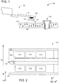
- FIG. 1 generally illustrates a block representation of an example data storage device 100 that can utilize a tuned magnetic element in accordance with various embodiments.
- the data storage device 100 is shown in a non-limiting configuration where an actuating assembly 102 is capable of positioning a transducing head 104 over a variety of locations on a magnetic storage media 106 where stored data bits 108 are located on predetermined data tracks.
- the storage media 106 can be attached to one or more spindle motors 110 that rotate during use to produce an air bearing surface (ABS) 112 on which a slider portion 114 of the actuating assembly 102 flies to position a head gimbal assembly (HGA) 116, which includes the transducing head 104, over a predetermined portion of the media 106.
- ABS air bearing surface
- HGA head gimbal assembly
- the transducing head 104 can be configured with one or more transducing elements, such as a magnetic writer, magnetically responsive reader, and magnetic shields, which operate to program and read data from the selected data tracks of the storage media 106, respectively.
- controlled motion of the actuating assembly 102 correspond with alignment of the transducers with the data tracks defined on the storage media surfaces to write, read, and rewrite data.
- the head 104 may inadvertently receive magnetic flux from data bits on adjacent data tracks, which can induce magnetic noise and interference that degrades performance of the data storage device 100.
- FIG. 2 displays a cross-sectional block representation of an example magnetic element 120 constructed with magnetic shielding to mitigate the effects of reduced form factor data tracks and more densely packed data bits. While the magnetic element 120 can have one or more data access elements, a magnetic data writer 122 portion of the magnetic element 120 is shown, which can operate to write data to from an adjacent storage media, such as media 106 of FIG. 1 .
- the magnetic data writer 122 has a main write pole 124 and at least one return pole 126 that creates a writing circuit to impart a predetermined magnetic orientation to the adjacent storage media. In the non-limiting configuration of the data writer 124 shown in FIG.
- two return poles 126 are each contactingly adjacent a trailing shield 128 that prevents flux in the poles 124 and 126 from extending beyond the bounds of the writing element 124.
- Each return pole 126 further contacts insulating material 132 that maintains magnetic separation of the writing poles 124 and 126.
- the various shields of the magnetic element 120 can be characterized by their position with respect to the timing of encountering external bits, such as bits 108 of FIG. 1 .
- the shields that encounter the external bits before the data writer 122 may be characterized as “leading” shields while shields that see the bits after the data writer 122 can be characterized as “trailing” shields.
- Such characterization extends to the difference between "uptrack” or “downtrack” of the transducing elements in that, depending on the direction of travel for the magnetic element 120 with respect to a data track 134 and external bits, the shields can be either leading or trailing and either uptrack or downtrack.
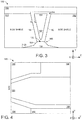
- FIG. 3 displays an ABS view block representation of a portion of an example data writer 150 constructed in accordance with various embodiments to have side 152, leading 154, and trailing 156 shields about a write pole 158.
- each side shield 152 is configured with tuned shield sidewalls 160 that are angled at a first predetermined orientation ⁇ 1 with respect to the Y axis and face a corresponding pole sidewall 162 tuned to a second predetermined angular orientation ⁇ 2 in relation to the Y axis.
- Various embodiments tune the shield 160 and pole 162 sidewalls to have matching or dissimilar angular orientations, which can provide a predetermined write gap 164 that can be uniform or varying distances from the write pole 158 to the respective side shields 152 to control magnetic performance of the write pole 158, such as the magnetic saturation of the side shields.
- FIG. 4 generally illustrates a cross-sectional block representation of a portion of a data writer 180 formed in accordance to some embodiments to have a write pole 182 disposed between leading 184 and trailing 186 shields on the ABS.
- the insertion of non-magnetic spacer 188 and gap 190 layers between the write pole 182 and the respective leading 184 and trailing 186 shields act in concert with the non-magnetic material filling the write gap 164 of FIG. 3 to provide a "box shield" where the write pole is surrounded by non-magnetic material and magnetic shields each tuned to provide a predetermined magnetic performance.
- the magnetic extent of the data writer 150 can be reduced to reliably program only predetermined data bits at the exclusion of data bits on adjacent data tracks.
- the addition of side shields can complicate write pole manufacturing and operation as intricate shapes and dimensions can be difficult to construct. More specifically, side shields and reduced data writer dimensions can make milling a write pole difficult compared to plating operations, which may result in degraded magnetic moment and magnetic flexibility.
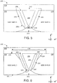
- FIG. 5 shows an ABS view block representation of a portion of an example data writer 190 having a box shield separated from the write pole 204 by a multi-layer gap structure 202 to be efficiently milled instead of plated.
- the multi-layer gap structure 202 is not limited to particular materials, number of layers, and orientation with respect to the write pole 204, but can consist of a non-magnetic gap layer 206, such as alumina, and a mill stop layer 208, such as a transition metal material like Ruthenium, as shown.
- a non-magnetic gap layer 206 and mill stop layer 208 between the write pole 204 and the respective side shields 210 can provide more robust magnetic isolation than a single layer of material, which can correspond to increased magnetic performance as reduced size write gap are employed, and allow for the write pole 204 to be manufactured via milling instead of plating as the mill stop layer 208 dictates where milling operations terminate.
- the complete surrounding of the write pole 204 with the non-magnetic material, such as Aluminum Oxide, of the non-magnetic gap layer 206, including the gap 212 between the trailing shield 214 and write pole 204, allows the magnetic side 210, leading 216, and trailing 214 shields to act as a unified box shield as the non-magnetic gap layer 206 and non-magnetic leading tip 218 of the magnetic leading shield 216 provides increased magnetic isolation of the write pole 204.
- the non-magnetic material such as Aluminum Oxide
- Such surrounding of the write pole 204 can be tuned in a variety of different manners, such as making the gap layer 206 and mill stop layer 208 different thickness overall or in selected portions of the write pole 204, to provide a predetermined amount of magnetic isolation of the write pole 204 in balance with reduced dimensions conducive to small form factor, high data bit density data storage devices.
- FIG. 6 provides an ABS view block representation of a portion of an example data writer 220 constructed with a box shield 222 and multi-layer structure 224 tuned differently than the multi-layer structure 202 of FIG. 5 , which generally illustrates the diversity of the multi-layer structure 222 when tuned in accordance with various embodiments.
- the multi-layer structure 224 has first 226 and second 228 non-magnetic gap layers separated by a mill stop layer 230. As shown, the second non-magnetic gap layer 228 is positioned proximal a trailing edge of the write pole 232 and contacting adjacent a letterbox 234 extension of the first non-magnetic gap layer 226.
- the size, material, and position of the second non-magnetic gap layer 228 can be tuned in a variety of ways, such as the displayed extension from the letterbox 234 to a point intermediate of the leading and trailing edges of the write pole, to provide predetermined operational characteristics like reduced magnetic saturation of the side shields 236.
- Such tuning can, in some embodiments, position multiple separated second non-magnetic gap layer 228 portions between the mill stop layer 230 and the side shields 236 to provide additional magnetic isolation of the write pole 232 in certain regions of the box shield 222.
- the operational characteristics of the data writer 220 may be further tuned by setting the width 238 of the letterbox 234, as measured along the Z axis, to a predetermined length.
- the width 238 can be greater than the distance between the second non-magnetic gap layers 228, but less than the overall width of the trailing shield 240.
- the multi-layer structure 224 can additionally allow for tuning of the interface between the leading edge of the write pole 232 and the leading shield 242 with a non-magnetic leading tip 244, which may include the angular configuration of a leading sidewall 246 of the side shields 236 to be different than the pole sidewall 248 of the write pole 232.
- leading sidewall 246 and leading shield 242 can be tuned with non-magnetic material 244 and angled orientations to provide a predetermined amount of magnetic isolation for the leading edge of the write pole 232 that may differ from the amount of magnetic isolation for the trailing edge.
- the use of multiple non-magnetic gap layers can provide the ability to tune the magnetic isolation of the write pole 232 through material selection.
- alumina may be used for the first gap layer 226 while SiO 2 is used for the second gap layer 228 to provide a varying magnetic gradient within the write gap 250.
- the data writer 220 can be catered to a variety of data environments by adjusting the magnetic isolation for portions of the write pole 232 to allow more, or less, isolation conducive to fast data accesses to densely packed data bits.
- FIGS. 7A and 7B provides an example data writer fabrication routine 260 conducted in accordance with various embodiments to tune the magnetic isolation of a write pole through the construction of a multi-layer structure.
- the routine 260 initially forms a leading shield in step 262, which is illustrated by element 280 with leading shield material 282 formed in a recess of a substrate 284.
- Steps 264 and 266 subsequently create a predetermined bevel configuration and form a write pole.
- Element 290 corresponds to steps 264 and 266 by having a beveled section and a write pole lamination that includes a non-magnetic spacer layer 292, a write pole material 294, and a write pole hard mask 296.
- Step 266 may further entail etching and milling of the write pole to provide a predetermined leading shield and write pole configuration such as the non-magnetic leading shield tip 298 shown by element 300.
- step 268 deposits the multi-layer gap structure with predetermined number of layers, materials, sizes, and positions.
- Element 310 displays a dual non-magnetic gap layer 312 and 314 separated by a mill stop layer 316 that each continuously extend to surround the write pole 294.
- step 270 proceeds to mill through some portions of the outside non-magnetic gap layer to the mill stop layer.
- the milling of step 270 can further include the planarization of the multi-layer gap structure and write pole hard mask from the trailing portion of the write pole, as shown in element 320.
- Conclusion of the milling operation can advance routine 260 to step 272 and element 330 where side shields 332 are formed on opposite sides of the write pole in contacting abutment with the multi-layer gap structure.
- step 276 deposits a letterbox mask shaped with a predetermined width to form the letterbox 334 after the trialing shield 336 is formed in step 278.
- a decision not to include a letterbox 334 can proceed to step 278 where a non-magnetic insert 338 is deposited atop the write pole to complete the multi-layer gap structure and magnetically isolate the write pole from the trailing shield 336.
- routine 260 a data writer can be constructed with tuned magnetic isolation of a write pole with a multi-layer gap structure. It should be noted, however, that the various steps and decisions of routine 260 shown in FIGS. 7A and 7B are not required or limited as the various decisions and steps can be omitted, changed, and added. As an example, an additional decision can be evaluated to determine how many layers are to be included in the multi-layer gap structure.
- magnetic performance of the write pole can be catered to provide heighted magnetic isolation in certain portions, like the trailing edge of the write pole, and reduced magnetic isolation in other portions, like the leading edge of the write pole.
- Such tuned multi-layer gap structure can further allow the use of milling operations to construct the write pole, which provides more robust magnetic performance versus a plated write pole.
- the ability to form a milled write pole with predetermined magnetic isolation in reduced form factor environments allows the data writer to be implemented in modern high data bit density, reduced form factor data storage devices.
Description
-
US 2010/301007 discloses a magnetic head that includes a pole layer, first and second side shields, and an encasing layer having first to third grooves that accommodate the pole layer and the first and second side shields. A manufacturing method for the magnetic head includes the step of forming the first to third grooves in a non-magnetic layer by using an etching mask layer having first to third openings. This step includes the steps of forming the first groove by etching the non-magnetic layer using the first opening, with the second and third openings covered with a first mask, and forming the second and third grooves by etching the non-magnetic layer using the second and third openings, with the first opening covered with a second mask.US2008088972 A1 discloses a magnetic head with a write pole within a box shield, the write pole separated from the box shield by a multi-layer gap structure according to the preamble of claim 1. - Various embodiments are generally directed to a magnetic element capable of being used in high data bit density data storage environments.
- According to a first aspect of the present invention, there is provided a magnetic data writer as defined in claim 1.
- Embodiments of the present invention will now be described by way of further example only and with reference to the accompanying drawings, in which:
-
FIG. 1 is a block representation of an example data storage device provided as background art only. -
FIG. 2 illustrates a cross-sectional block representation of an example magnetic element capable of being used in the data storage device ofFIG. 1 . -
FIG. 3 shows an ABS view block representation of a portion of an example magnetic element provided as background art only. -
FIG. 4 displays a cross-sectional block representation of an example magnetic element provided as background art only. -
FIG. 5 illustrates an ABS view block representation of a portion of an example magnetic element provided as background art only. -
FIG. 6 is an ABS view block representation of a portion of an example magnetic element constructed in accordance with the claimed invention. -
FIGS. 7A and 7B provide a flowchart and associated illustrations for an example data writer fabrication routine in accordance with various embodiments. - The embodiments shown in
Figs. 1 to 5 do not form part of the claimed invention and are provided as background art only. Only the embodiments described below in relation toFigs. 6 ,7A and 7B form part of the claimed invention. - The proliferation of data usage has emphasized the form factor and data capacity of data storage devices, especially devices with faster data access times and increased data access reliability. Increasing data storage capacity in combination with fast data access times may correspond with smaller data access components, such as data reader laminations and data write poles, and increasingly robust magnetic shielding. However, shielding of plated components can impose process and design complexity that may detrimentally affect magnetic performance, such as magnetic field gradient, magnetic moment, and magnetic properties flexibility. Conversely, the use of a milled data access component can maintain magnetic performance, but pose difficult construction with shaped components, like trapezoidal shaped write poles. Thusly, there is a continued industry demand for magnetic shield configurations capable of being implemented with milled in reduced form factor data storage devices without decreasing magnetic field and gradient.
- Accordingly, a magnetic element can be configured in accordance with various embodiments to have at least a write pole within a box shield that consists of first and second side shields and first and second vertical shields, where the write pole may be separated from the box shield by a multi-layer gap structure that consists of at least two gap layers of dissimilar materials. The use of dissimilar gap layers allows for the magnetic and physical isolation of the write pole from the shields while providing a mill stop layer that aids in shaping the write pole without plating processes. Such a shaped and milled write pole can provide high write field gradient and reduced adjacent track interference that has robust magnetic shielding.
- The use of a multi-layer box shield about a write pole is not limited to a particular environment, but
FIG. 1 generally illustrates a block representation of an exampledata storage device 100 that can utilize a tuned magnetic element in accordance with various embodiments. Thedata storage device 100 is shown in a non-limiting configuration where anactuating assembly 102 is capable of positioning a transducinghead 104 over a variety of locations on amagnetic storage media 106 where storeddata bits 108 are located on predetermined data tracks. Thestorage media 106 can be attached to one ormore spindle motors 110 that rotate during use to produce an air bearing surface (ABS) 112 on which aslider portion 114 of theactuating assembly 102 flies to position a head gimbal assembly (HGA) 116, which includes the transducinghead 104, over a predetermined portion of themedia 106. - The transducing
head 104 can be configured with one or more transducing elements, such as a magnetic writer, magnetically responsive reader, and magnetic shields, which operate to program and read data from the selected data tracks of thestorage media 106, respectively. In this way, controlled motion of the actuatingassembly 102 correspond with alignment of the transducers with the data tracks defined on the storage media surfaces to write, read, and rewrite data. Asdata bits 108 become more densely positioned in data tracks with smaller radial widths, thehead 104 may inadvertently receive magnetic flux from data bits on adjacent data tracks, which can induce magnetic noise and interference that degrades performance of thedata storage device 100. -
FIG. 2 displays a cross-sectional block representation of an examplemagnetic element 120 constructed with magnetic shielding to mitigate the effects of reduced form factor data tracks and more densely packed data bits. While themagnetic element 120 can have one or more data access elements, amagnetic data writer 122 portion of themagnetic element 120 is shown, which can operate to write data to from an adjacent storage media, such asmedia 106 ofFIG. 1 . Themagnetic data writer 122 has amain write pole 124 and at least onereturn pole 126 that creates a writing circuit to impart a predetermined magnetic orientation to the adjacent storage media. In the non-limiting configuration of thedata writer 124 shown inFIG. 2 , tworeturn poles 126 are each contactingly adjacent atrailing shield 128 that prevents flux in thepoles writing element 124. Eachreturn pole 126 furthercontacts insulating material 132 that maintains magnetic separation of thewriting poles - The various shields of the
magnetic element 120 can be characterized by their position with respect to the timing of encountering external bits, such asbits 108 ofFIG. 1 . In other words, the shields that encounter the external bits before thedata writer 122 may be characterized as "leading" shields while shields that see the bits after thedata writer 122 can be characterized as "trailing" shields. Such characterization extends to the difference between "uptrack" or "downtrack" of the transducing elements in that, depending on the direction of travel for themagnetic element 120 with respect to adata track 134 and external bits, the shields can be either leading or trailing and either uptrack or downtrack. - While the
magnetic element 120 has a plurality of magnetic shields configured to focus magnetic flux from thewrite pole 124 to a predetermined data bit along a data track, increased data bit densities have led to the tighter data tracks that can impose magnetic flux on data bits along the Z axis. The addition of side shields in the Z axis with respect to thewrite pole 124 can tune the magnetic extent of thewrite pole 124 to conform to a reduced data track width.FIG. 3 displays an ABS view block representation of a portion of anexample data writer 150 constructed in accordance with various embodiments to haveside 152, leading 154, and trailing 156 shields about awrite pole 158. - As shown, each
side shield 152 is configured with tunedshield sidewalls 160 that are angled at a first predetermined orientation θ1 with respect to the Y axis and face acorresponding pole sidewall 162 tuned to a second predetermined angular orientation θ2 in relation to the Y axis. Various embodiments tune theshield 160 andpole 162 sidewalls to have matching or dissimilar angular orientations, which can provide apredetermined write gap 164 that can be uniform or varying distances from thewrite pole 158 to therespective side shields 152 to control magnetic performance of thewrite pole 158, such as the magnetic saturation of the side shields. - One, or both,
side shields 152 can be further configured with atapered feature 166 that provides at least onetaper sidewall 168 that increases the distance between theside shields 152 downtrack from thewrite pole 158, which may be occupied partially or wholly by atip 170 of the leadingshield 154.FIG. 4 generally illustrates a cross-sectional block representation of a portion of adata writer 180 formed in accordance to some embodiments to have awrite pole 182 disposed between leading 184 and trailing 186 shields on the ABS. The insertion ofnon-magnetic spacer 188 andgap 190 layers between thewrite pole 182 and the respective leading 184 and trailing 186 shields act in concert with the non-magnetic material filling thewrite gap 164 ofFIG. 3 to provide a "box shield" where the write pole is surrounded by non-magnetic material and magnetic shields each tuned to provide a predetermined magnetic performance. - Through the tuned configuration of the various shields with respect to the
write pole 158, the magnetic extent of thedata writer 150 can be reduced to reliably program only predetermined data bits at the exclusion of data bits on adjacent data tracks. However, the addition of side shields can complicate write pole manufacturing and operation as intricate shapes and dimensions can be difficult to construct. More specifically, side shields and reduced data writer dimensions can make milling a write pole difficult compared to plating operations, which may result in degraded magnetic moment and magnetic flexibility. - With such manufacturing issues in mind,
FIG. 5 shows an ABS view block representation of a portion of anexample data writer 190 having a box shield separated from thewrite pole 204 by amulti-layer gap structure 202 to be efficiently milled instead of plated. Themulti-layer gap structure 202 is not limited to particular materials, number of layers, and orientation with respect to thewrite pole 204, but can consist of anon-magnetic gap layer 206, such as alumina, and amill stop layer 208, such as a transition metal material like Ruthenium, as shown. The combination of anon-magnetic gap layer 206 andmill stop layer 208 between thewrite pole 204 and therespective side shields 210 can provide more robust magnetic isolation than a single layer of material, which can correspond to increased magnetic performance as reduced size write gap are employed, and allow for thewrite pole 204 to be manufactured via milling instead of plating as themill stop layer 208 dictates where milling operations terminate. - In the past, milling of such a precise shape and dimensions would be time consuming and complex undertaking due at least in part to the intricate sidewall angles of the write pole and side shields, as illustrated in
FIG. 3 . The daunting and unpractical milling of thewrite pole 204 leads to a plating construction where a groove with a predetermined shape is filled. However, the lower magnetic moment and reduced magnetic flexibility corresponding to plated write poles can pose operational limitations as magnetic components become more condensed in reduced form factor data storage devices. Thus, the inclusion of at least onemill stop layer 208 in themulti-layer structure 202 can minimize manufacturing complexity and allow for the milled construction of thewrite pole 204. - While the orientation and material of the various
multi-layer structure 202 layers is not limited to the configuration shown inFIG. 5 , the complete surrounding of thewrite pole 204 with the non-magnetic material, such as Aluminum Oxide, of thenon-magnetic gap layer 206, including thegap 212 between thetrailing shield 214 and writepole 204, allows themagnetic side 210, leading 216, and trailing 214 shields to act as a unified box shield as thenon-magnetic gap layer 206 and non-magnetic leadingtip 218 of the magnetic leadingshield 216 provides increased magnetic isolation of thewrite pole 204. Such surrounding of thewrite pole 204 can be tuned in a variety of different manners, such as making thegap layer 206 andmill stop layer 208 different thickness overall or in selected portions of thewrite pole 204, to provide a predetermined amount of magnetic isolation of thewrite pole 204 in balance with reduced dimensions conducive to small form factor, high data bit density data storage devices. -
FIG. 6 provides an ABS view block representation of a portion of anexample data writer 220 constructed with abox shield 222 andmulti-layer structure 224 tuned differently than themulti-layer structure 202 ofFIG. 5 , which generally illustrates the diversity of themulti-layer structure 222 when tuned in accordance with various embodiments. Themulti-layer structure 224 has first 226 and second 228 non-magnetic gap layers separated by amill stop layer 230. As shown, the secondnon-magnetic gap layer 228 is positioned proximal a trailing edge of thewrite pole 232 and contacting adjacent aletterbox 234 extension of the firstnon-magnetic gap layer 226. - The size, material, and position of the second
non-magnetic gap layer 228 can be tuned in a variety of ways, such as the displayed extension from the letterbox 234 to a point intermediate of the leading and trailing edges of the write pole, to provide predetermined operational characteristics like reduced magnetic saturation of the side shields 236. Such tuning can, in some embodiments, position multiple separated secondnon-magnetic gap layer 228 portions between themill stop layer 230 and the side shields 236 to provide additional magnetic isolation of thewrite pole 232 in certain regions of thebox shield 222. - The operational characteristics of the
data writer 220 may be further tuned by setting thewidth 238 of the letterbox 234, as measured along the Z axis, to a predetermined length. For example, thewidth 238 can be greater than the distance between the second non-magnetic gap layers 228, but less than the overall width of the trailingshield 240. Themulti-layer structure 224 can additionally allow for tuning of the interface between the leading edge of thewrite pole 232 and the leadingshield 242 with a non-magneticleading tip 244, which may include the angular configuration of a leadingsidewall 246 of the side shields 236 to be different than thepole sidewall 248 of thewrite pole 232. That is, the leadingsidewall 246 and leadingshield 242 can be tuned withnon-magnetic material 244 and angled orientations to provide a predetermined amount of magnetic isolation for the leading edge of thewrite pole 232 that may differ from the amount of magnetic isolation for the trailing edge. - The use of multiple non-magnetic gap layers can provide the ability to tune the magnetic isolation of the
write pole 232 through material selection. As a non-limiting example, alumina may be used for thefirst gap layer 226 while SiO2 is used for thesecond gap layer 228 to provide a varying magnetic gradient within thewrite gap 250. Through these diversemulti-layer structure 224 tuning options, thedata writer 220 can be catered to a variety of data environments by adjusting the magnetic isolation for portions of thewrite pole 232 to allow more, or less, isolation conducive to fast data accesses to densely packed data bits. - With the variety of non-limiting multi-layer structure configurations possible to optimize write pole performance, the construction of a magnetic element can undergo a series of general and specific decisions to tune the magnetic operation.
FIGS. 7A and 7B provides an example datawriter fabrication routine 260 conducted in accordance with various embodiments to tune the magnetic isolation of a write pole through the construction of a multi-layer structure. The routine 260 initially forms a leading shield instep 262, which is illustrated by element 280 with leadingshield material 282 formed in a recess of asubstrate 284. -
Steps Element 290 corresponds tosteps non-magnetic spacer layer 292, awrite pole material 294, and a write polehard mask 296. Step 266 may further entail etching and milling of the write pole to provide a predetermined leading shield and write pole configuration such as the non-magneticleading shield tip 298 shown byelement 300. Next, step 268 deposits the multi-layer gap structure with predetermined number of layers, materials, sizes, and positions.Element 310 displays a dualnon-magnetic gap layer mill stop layer 316 that each continuously extend to surround thewrite pole 294. - With the multi-layer gap structure deposited, step 270 proceeds to mill through some portions of the outside non-magnetic gap layer to the mill stop layer. The milling of
step 270 can further include the planarization of the multi-layer gap structure and write pole hard mask from the trailing portion of the write pole, as shown in element 320. Conclusion of the milling operation can advance routine 260 to step 272 andelement 330 where side shields 332 are formed on opposite sides of the write pole in contacting abutment with the multi-layer gap structure. - Formation of the side shields brings routine 260 to
decision 274 where the inclusion of a letterbox 334 is evaluated. If a letterbox 334 is chosen indecision 274, step 276 deposits a letterbox mask shaped with a predetermined width to form the letterbox 334 after thetrialing shield 336 is formed instep 278. A decision not to include a letterbox 334 can proceed to step 278 where anon-magnetic insert 338 is deposited atop the write pole to complete the multi-layer gap structure and magnetically isolate the write pole from the trailingshield 336. - Through the various steps and decisions of routine 260, a data writer can be constructed with tuned magnetic isolation of a write pole with a multi-layer gap structure. It should be noted, however, that the various steps and decisions of routine 260 shown in
FIGS. 7A and 7B are not required or limited as the various decisions and steps can be omitted, changed, and added. As an example, an additional decision can be evaluated to determine how many layers are to be included in the multi-layer gap structure. - With the tuned configuration of the multi-layer gap structure, magnetic performance of the write pole can be catered to provide heighted magnetic isolation in certain portions, like the trailing edge of the write pole, and reduced magnetic isolation in other portions, like the leading edge of the write pole. Such tuned multi-layer gap structure can further allow the use of milling operations to construct the write pole, which provides more robust magnetic performance versus a plated write pole. The ability to form a milled write pole with predetermined magnetic isolation in reduced form factor environments allows the data writer to be implemented in modern high data bit density, reduced form factor data storage devices.
- In addition, while the embodiments have been directed to magnetic programming, it will be appreciated that the claimed invention can readily be utilized in any number of other applications, including data storage device applications. It is to be understood that even though numerous characteristics and configurations of various embodiments of the present disclosure have been set forth in the foregoing description, together with details of the structure and function of various embodiments, this detailed description is illustrative only, and changes may be made in detail, especially in matters of structure and arrangements of parts within the principles of the present disclosure to the full extent indicated by the broad general meaning of the terms in which the appended claims are expressed. For example, the particular elements may vary depending on the particular application without departing from the scope of the present technology.
- It is should noted that where the claims refer to an apparatus, non-limiting examples of such an apparatus include a magnetic element or a data writer, components of these, or any other suitable apparatus.
Claims (14)
- A magnetic data writer (220) comprising a write pole (232) within a box shield comprising first and second side shields (236) and first and second vertical shields (240, 242), the write pole being separated from the box shield by a multi-layer gap structure,
wherein the multi-layer gap structure physically connects each shield with the pole layer and comprises first (226) and second (228) non-magnetic gap layers separated by a mill stop layer (230), at least two of the non-magnetic gap and mill stop layers being formed of dissimilar materials, and
wherein the first non-magnetic gap layer (226) continuously extends to surround and contact the whole write pole, and extends beyond a write gap region into a letterbox region (234) between the trailing and side shields (240, 236) characterized in that the mill stop layer (230) is disposed only along both sides of the write pole over the first non-magnetic gap layer and contacts, among the side and vertical shields, only the side shields (236), and
the second non-magnetic gap layer (228) is positioned proximal a trailing edge of the write pole, between mill stop layer and side shield, only at both sides of the write pole, and configured to extend from the letterbox (234) only to a point intermediate the trailing edge and a leading edge of the write pole. - The magnetic data writer (220) of claim 1, wherein the multi-layer gap structure physically connects each shield with the write pole.
- The magnetic data writer (220) of claim 1 or claim 2, wherein the mill stop layer comprises Ruthenium.
- The magnetic data writer (220) of any of claims 1 to 3, wherein the non-magnetic layer is alumina.
- The magnetic data writer (220) of any one of the preceding claims, wherein less than all the gap layers surround the write pole.
- The magnetic data writer (220) of any one of the preceding claims, wherein the multi-layer gap structure is positioned on an air bearing surface (ABS).
- The magnetic data writer (220) of any one of the preceding claims, wherein the gap layers each have a gap sidewall angularly oriented to match a pole sidewall.
- The magnetic data writer (220) of any one of the preceding claims, wherein the gap layers each have unique thicknesses.
- The magnetic data writer (220) of any one of the preceding claims, wherein the second non-magnetic gap layer (228) has a first gap sidewall that has a different angular orientation than a second gap sidewall of the first non-magnetic gap layer (226).
- The magnetic data writer (220) of any one of the preceding claims, wherein the first non-magnetic gap layer extends beyond a write gap region into a letterbox region (234) between the trailing and side shields (240, 236).
- The magnetic data writer (220) of any one of the preceding claims, wherein the first and second non-magnetic gap layers are formed of dissimilar materials.
- The magnetic data writer (200) of any one of the preceding claims, wherein at least one gap layer of the multi-layer gap structure extends to a letterbox region (234) between the side and trailing shields (236, 240).
- The magnetic data writer (200) of claim 12, wherein the letterbox has a predetermined width (238) greater than a gap width between the side shields.
- The magnetic data writer (200) of claim 12 or claim 13, wherein the letterbox is formed with the union of at least one side shield (236) and a trailing shield (240).
Applications Claiming Priority (1)
| Application Number | Priority Date | Filing Date | Title |
|---|---|---|---|
| US13/745,031 US8842390B2 (en) | 2013-01-18 | 2013-01-18 | Write pole box shield |
Publications (3)
| Publication Number | Publication Date |
|---|---|
| EP2757561A2 EP2757561A2 (en) | 2014-07-23 |
| EP2757561A3 EP2757561A3 (en) | 2015-01-07 |
| EP2757561B1 true EP2757561B1 (en) | 2017-05-03 |
Family
ID=49955226
Family Applications (1)
| Application Number | Title | Priority Date | Filing Date |
|---|---|---|---|
| EP14151657.5A Not-in-force EP2757561B1 (en) | 2013-01-18 | 2014-01-17 | Write pole box shield |
Country Status (5)
| Country | Link |
|---|---|
| US (1) | US8842390B2 (en) |
| EP (1) | EP2757561B1 (en) |
| JP (1) | JP6050266B2 (en) |
| KR (1) | KR101563218B1 (en) |
| CN (1) | CN103943115B (en) |
Families Citing this family (14)
| Publication number | Priority date | Publication date | Assignee | Title |
|---|---|---|---|---|
| US9147407B2 (en) * | 2013-03-12 | 2015-09-29 | Seagate Technology Llc | Write head having non-magnetic write gap seed layer, and method |
| US9214167B2 (en) | 2013-03-12 | 2015-12-15 | Seagate Technology Llc | Main pole layer with at least tow sacrificial layers and a gap layer |
| US9047889B1 (en) * | 2013-12-10 | 2015-06-02 | HGST Netherlands B.V. | Perpendicular magnetic recording head having a trailing side taper angle which is less than a leading side taper angle |
| US8988824B1 (en) * | 2013-12-23 | 2015-03-24 | HGST Netherlands B.V. | Method for manufacturing a magnetic write pole with a consistent bevel angle |
| US9001465B1 (en) * | 2014-04-16 | 2015-04-07 | HGST Netherlands B.V. | Microwave-assisted magnetic recording head |
| US9214165B1 (en) * | 2014-12-18 | 2015-12-15 | Western Digital (Fremont), Llc | Magnetic writer having a gradient in saturation magnetization of the shields |
| US9741366B1 (en) | 2014-12-18 | 2017-08-22 | Western Digital (Fremont), Llc | Method for fabricating a magnetic writer having a gradient in saturation magnetization of the shields |
| US9443541B1 (en) | 2015-03-24 | 2016-09-13 | Western Digital (Fremont), Llc | Magnetic writer having a gradient in saturation magnetization of the shields and return pole |
| US9984707B2 (en) | 2015-11-11 | 2018-05-29 | Seagate Technology Llc | Write pole wrap-around shield with gap lamination |
| JP6527480B2 (en) * | 2016-03-04 | 2019-06-05 | 株式会社東芝 | Magnetic recording head and magnetic recording apparatus |
| US10026423B1 (en) | 2017-05-01 | 2018-07-17 | Seagate Technology Llc | Moderate mill resist and wet-etchable alloy for use in a recording head fabrication process |
| US10229703B2 (en) * | 2017-05-15 | 2019-03-12 | Headway Technologies, Inc. | PMR write head with patterned leading edge taper |
| US10586559B1 (en) * | 2018-12-11 | 2020-03-10 | Seagate Technology Llc | Side shield formation |
| US10832710B1 (en) * | 2019-09-09 | 2020-11-10 | Western Digital Technologies, Inc. | Magnetic recording devices using virtual side shields for improved areal density capability |
Family Cites Families (22)
| Publication number | Priority date | Publication date | Assignee | Title |
|---|---|---|---|---|
| US5568335A (en) | 1994-12-29 | 1996-10-22 | International Business Machines Corporation | Multi-layer gap structure for high resolution magnetoresistive read head |
| US7233457B2 (en) * | 2003-12-16 | 2007-06-19 | Seagate Technology Llc | Head for perpendicular recording with reduced erasure |
| US7414816B2 (en) * | 2004-05-28 | 2008-08-19 | Hitachi Global Storage Technologies Netherlands B.V. | Planar magnetic thin film head |
| JP2006252620A (en) * | 2005-03-09 | 2006-09-21 | Hitachi Global Storage Technologies Netherlands Bv | Magnetic head and its manufacturing method |
| US7633714B2 (en) * | 2006-07-26 | 2009-12-15 | Headway Technologies, Inc. | Magnetic head for perpendicular magnetic recording and method of manufacturing same |
| US8467147B2 (en) * | 2006-10-13 | 2013-06-18 | Headway Technologies, Inc. | Magnetic head for perpendicular magnetic recording and method of manufacturing same |
| US7804666B2 (en) * | 2007-04-13 | 2010-09-28 | Headway Technologies, Inc. | Composite shield structure of PMR writer for high track density |
| US8051552B2 (en) * | 2007-05-11 | 2011-11-08 | Hitachi Global Storage Technologies Netherlands, B.V. | Stitched wrap around shield fabrication for perpendicular magnetic recording write heads |
| US7990651B2 (en) * | 2007-12-13 | 2011-08-02 | Hitachi Global Storage Technologies Netherlands B.V. | Method of manufacturing a perpendicular magnetic write head with stepped trailing magnetic shield with electrical lapping guide control |
| US8049989B2 (en) * | 2007-12-26 | 2011-11-01 | Hitachi Global Storage Technologies Netherlands B.V. | Magnetic head for perpendicular recording having stepped wrap around shield with independent control of write pole track width and flare point dimensions |
| US8166631B1 (en) * | 2008-08-27 | 2012-05-01 | Western Digital (Fremont), Llc | Method for fabricating a magnetic recording transducer having side shields |
| US8031433B2 (en) * | 2008-09-05 | 2011-10-04 | Headway Technologies, Inc. | Method to make an integrated side shield PMR head with non conformal side gap |
| US8289648B2 (en) | 2009-02-20 | 2012-10-16 | Seagate Technology Llc | Magnetic recording head with layered structure in write gap |
| US8173028B2 (en) * | 2009-06-01 | 2012-05-08 | Headway Technologies, Inc. | Method of manufacturing magnetic head for perpendicular magnetic recording including two side shields |
| US8358486B2 (en) * | 2009-10-13 | 2013-01-22 | International Business Machines Corporation | Magnetically shielded write transducers |
| US8842389B2 (en) * | 2009-10-26 | 2014-09-23 | Headway Technologies, Inc. | Wrap-around shielded writer with highly homogeneous shield material |
| US8094399B2 (en) * | 2010-03-10 | 2012-01-10 | Tdk Corporation | Magnetic recording apparatus provided with microwave-assisted head |
| US8611046B2 (en) * | 2010-04-19 | 2013-12-17 | Headway Technologies, Inc. | PMR writer with graded side shield |
| US8355222B2 (en) * | 2010-06-30 | 2013-01-15 | Sae Magnetics (H.K.) Ltd. | Perpendicular magnetic write head including high magnetic moment seed layer for trailing shield therein and/or method of making the same |
| US8347489B2 (en) * | 2010-09-01 | 2013-01-08 | Hitachi Global Storage Technologies Netherlands B.V. | Method for manufacturing a perpendicular magnetic write head having a leading edge tapered write pole, self aligned side shield and independent trailing shield |
| US8470186B2 (en) * | 2010-11-24 | 2013-06-25 | HGST Netherlands B.V. | Perpendicular write head with wrap around shield and conformal side gap |
| US8238059B1 (en) * | 2011-04-06 | 2012-08-07 | Headway Technologies, Inc. | PMR write head with narrow gap for minimal internal flux loss |
-
2013
- 2013-01-18 US US13/745,031 patent/US8842390B2/en active Active
-
2014
- 2014-01-16 KR KR1020140005611A patent/KR101563218B1/en active IP Right Grant
- 2014-01-17 JP JP2014006524A patent/JP6050266B2/en not_active Expired - Fee Related
- 2014-01-17 CN CN201410022347.6A patent/CN103943115B/en not_active Expired - Fee Related
- 2014-01-17 EP EP14151657.5A patent/EP2757561B1/en not_active Not-in-force
Also Published As
| Publication number | Publication date |
|---|---|
| CN103943115A (en) | 2014-07-23 |
| US20140204485A1 (en) | 2014-07-24 |
| EP2757561A3 (en) | 2015-01-07 |
| JP2014149905A (en) | 2014-08-21 |
| JP6050266B2 (en) | 2016-12-21 |
| EP2757561A2 (en) | 2014-07-23 |
| KR101563218B1 (en) | 2015-10-26 |
| CN103943115B (en) | 2017-09-26 |
| US8842390B2 (en) | 2014-09-23 |
| KR20140093625A (en) | 2014-07-28 |
Similar Documents
| Publication | Publication Date | Title |
|---|---|---|
| EP2757561B1 (en) | Write pole box shield | |
| US8699183B2 (en) | Write pole and shield with different taper angles | |
| US9196267B2 (en) | Data writer with flux density insert | |
| US8830626B2 (en) | Write pole with shaped box shield | |
| EP2738764B1 (en) | Data writer with tapered side shield sidewalls | |
| JP4745892B2 (en) | Structure for thin film magnetic head, method of manufacturing the same, and thin film magnetic head | |
| US9437220B2 (en) | Varying data writer side shield gap distal the ABS | |
| JP2007287313A (en) | Thin film magnetic head, its manufacturing method, and head gimbal assembly, and hard disk drive | |
| US9984707B2 (en) | Write pole wrap-around shield with gap lamination | |
| EP2779167A2 (en) | Bottom shield stabilized magnetic seed layer | |
| US9019659B1 (en) | Write pole with varying bevel angles | |
| EP2728579A2 (en) | Magnetic element with current constriction feature | |
| US9396741B1 (en) | Data writer side shield with cantilevered protrusions | |
| US8995096B2 (en) | Magnetic element side shield with diffusion barrier | |
| US9224407B2 (en) | Varying write pole side shield gap | |
| US9721590B2 (en) | Varying write pole side shield gap | |
| US9734855B1 (en) | Data writer gap material with decreased protrusion | |
| US9922670B1 (en) | Method of manufacturing a recessed data reader pinning structure with vertical sidewall | |
| US9728207B2 (en) | Write pole magnetic guard |
Legal Events
| Date | Code | Title | Description |
|---|---|---|---|
| PUAI | Public reference made under article 153(3) epc to a published international application that has entered the european phase |
Free format text: ORIGINAL CODE: 0009012 |
|
| 17P | Request for examination filed |
Effective date: 20140117 |
|
| AK | Designated contracting states |
Kind code of ref document: A2 Designated state(s): AL AT BE BG CH CY CZ DE DK EE ES FI FR GB GR HR HU IE IS IT LI LT LU LV MC MK MT NL NO PL PT RO RS SE SI SK SM TR |
|
| AX | Request for extension of the european patent |
Extension state: BA ME |
|
| PUAL | Search report despatched |
Free format text: ORIGINAL CODE: 0009013 |
|
| AK | Designated contracting states |
Kind code of ref document: A3 Designated state(s): AL AT BE BG CH CY CZ DE DK EE ES FI FR GB GR HR HU IE IS IT LI LT LU LV MC MK MT NL NO PL PT RO RS SE SI SK SM TR |
|
| AX | Request for extension of the european patent |
Extension state: BA ME |
|
| RIC1 | Information provided on ipc code assigned before grant |
Ipc: G11B 5/31 20060101AFI20141128BHEP |
|
| RBV | Designated contracting states (corrected) |
Designated state(s): AL AT BE BG CH CY CZ DE DK EE ES FI FR GB GR HR HU IE IS IT LI LT LU LV MC MK MT NL NO PL PT RO RS SE SI SK SM TR |
|
| 17Q | First examination report despatched |
Effective date: 20160120 |
|
| RIC1 | Information provided on ipc code assigned before grant |
Ipc: G11B 5/31 20060101AFI20160831BHEP Ipc: G11B 5/115 20060101ALI20160831BHEP Ipc: G11B 5/127 20060101ALI20160831BHEP Ipc: G11B 5/23 20060101ALI20160831BHEP |
|
| GRAP | Despatch of communication of intention to grant a patent |
Free format text: ORIGINAL CODE: EPIDOSNIGR1 |
|
| INTG | Intention to grant announced |
Effective date: 20161117 |
|
| GRAS | Grant fee paid |
Free format text: ORIGINAL CODE: EPIDOSNIGR3 |
|
| GRAA | (expected) grant |
Free format text: ORIGINAL CODE: 0009210 |
|
| AK | Designated contracting states |
Kind code of ref document: B1 Designated state(s): AL AT BE BG CH CY CZ DE DK EE ES FI FR GB GR HR HU IE IS IT LI LT LU LV MC MK MT NL NO PL PT RO RS SE SI SK SM TR |
|
| REG | Reference to a national code |
Ref country code: GB Ref legal event code: FG4D |
|
| REG | Reference to a national code |
Ref country code: AT Ref legal event code: REF Ref document number: 890796 Country of ref document: AT Kind code of ref document: T Effective date: 20170515 Ref country code: CH Ref legal event code: EP |
|
| REG | Reference to a national code |
Ref country code: IE Ref legal event code: FG4D |
|
| REG | Reference to a national code |
Ref country code: DE Ref legal event code: R096 Ref document number: 602014009160 Country of ref document: DE |
|
| REG | Reference to a national code |
Ref country code: NL Ref legal event code: MP Effective date: 20170503 |
|
| REG | Reference to a national code |
Ref country code: AT Ref legal event code: MK05 Ref document number: 890796 Country of ref document: AT Kind code of ref document: T Effective date: 20170503 |
|
| REG | Reference to a national code |
Ref country code: LT Ref legal event code: MG4D |
|
| PG25 | Lapsed in a contracting state [announced via postgrant information from national office to epo] |
Ref country code: GR Free format text: LAPSE BECAUSE OF FAILURE TO SUBMIT A TRANSLATION OF THE DESCRIPTION OR TO PAY THE FEE WITHIN THE PRESCRIBED TIME-LIMIT Effective date: 20170804 Ref country code: LT Free format text: LAPSE BECAUSE OF FAILURE TO SUBMIT A TRANSLATION OF THE DESCRIPTION OR TO PAY THE FEE WITHIN THE PRESCRIBED TIME-LIMIT Effective date: 20170503 Ref country code: ES Free format text: LAPSE BECAUSE OF FAILURE TO SUBMIT A TRANSLATION OF THE DESCRIPTION OR TO PAY THE FEE WITHIN THE PRESCRIBED TIME-LIMIT Effective date: 20170503 Ref country code: FI Free format text: LAPSE BECAUSE OF FAILURE TO SUBMIT A TRANSLATION OF THE DESCRIPTION OR TO PAY THE FEE WITHIN THE PRESCRIBED TIME-LIMIT Effective date: 20170503 Ref country code: AT Free format text: LAPSE BECAUSE OF FAILURE TO SUBMIT A TRANSLATION OF THE DESCRIPTION OR TO PAY THE FEE WITHIN THE PRESCRIBED TIME-LIMIT Effective date: 20170503 Ref country code: HR Free format text: LAPSE BECAUSE OF FAILURE TO SUBMIT A TRANSLATION OF THE DESCRIPTION OR TO PAY THE FEE WITHIN THE PRESCRIBED TIME-LIMIT Effective date: 20170503 Ref country code: NO Free format text: LAPSE BECAUSE OF FAILURE TO SUBMIT A TRANSLATION OF THE DESCRIPTION OR TO PAY THE FEE WITHIN THE PRESCRIBED TIME-LIMIT Effective date: 20170803 |
|
| PG25 | Lapsed in a contracting state [announced via postgrant information from national office to epo] |
Ref country code: SE Free format text: LAPSE BECAUSE OF FAILURE TO SUBMIT A TRANSLATION OF THE DESCRIPTION OR TO PAY THE FEE WITHIN THE PRESCRIBED TIME-LIMIT Effective date: 20170503 Ref country code: IS Free format text: LAPSE BECAUSE OF FAILURE TO SUBMIT A TRANSLATION OF THE DESCRIPTION OR TO PAY THE FEE WITHIN THE PRESCRIBED TIME-LIMIT Effective date: 20170903 Ref country code: RS Free format text: LAPSE BECAUSE OF FAILURE TO SUBMIT A TRANSLATION OF THE DESCRIPTION OR TO PAY THE FEE WITHIN THE PRESCRIBED TIME-LIMIT Effective date: 20170503 Ref country code: BG Free format text: LAPSE BECAUSE OF FAILURE TO SUBMIT A TRANSLATION OF THE DESCRIPTION OR TO PAY THE FEE WITHIN THE PRESCRIBED TIME-LIMIT Effective date: 20170803 Ref country code: NL Free format text: LAPSE BECAUSE OF FAILURE TO SUBMIT A TRANSLATION OF THE DESCRIPTION OR TO PAY THE FEE WITHIN THE PRESCRIBED TIME-LIMIT Effective date: 20170503 Ref country code: LV Free format text: LAPSE BECAUSE OF FAILURE TO SUBMIT A TRANSLATION OF THE DESCRIPTION OR TO PAY THE FEE WITHIN THE PRESCRIBED TIME-LIMIT Effective date: 20170503 Ref country code: PL Free format text: LAPSE BECAUSE OF FAILURE TO SUBMIT A TRANSLATION OF THE DESCRIPTION OR TO PAY THE FEE WITHIN THE PRESCRIBED TIME-LIMIT Effective date: 20170503 |
|
| PG25 | Lapsed in a contracting state [announced via postgrant information from national office to epo] |
Ref country code: EE Free format text: LAPSE BECAUSE OF FAILURE TO SUBMIT A TRANSLATION OF THE DESCRIPTION OR TO PAY THE FEE WITHIN THE PRESCRIBED TIME-LIMIT Effective date: 20170503 Ref country code: CZ Free format text: LAPSE BECAUSE OF FAILURE TO SUBMIT A TRANSLATION OF THE DESCRIPTION OR TO PAY THE FEE WITHIN THE PRESCRIBED TIME-LIMIT Effective date: 20170503 Ref country code: SK Free format text: LAPSE BECAUSE OF FAILURE TO SUBMIT A TRANSLATION OF THE DESCRIPTION OR TO PAY THE FEE WITHIN THE PRESCRIBED TIME-LIMIT Effective date: 20170503 Ref country code: RO Free format text: LAPSE BECAUSE OF FAILURE TO SUBMIT A TRANSLATION OF THE DESCRIPTION OR TO PAY THE FEE WITHIN THE PRESCRIBED TIME-LIMIT Effective date: 20170503 Ref country code: DK Free format text: LAPSE BECAUSE OF FAILURE TO SUBMIT A TRANSLATION OF THE DESCRIPTION OR TO PAY THE FEE WITHIN THE PRESCRIBED TIME-LIMIT Effective date: 20170503 |
|
| REG | Reference to a national code |
Ref country code: DE Ref legal event code: R097 Ref document number: 602014009160 Country of ref document: DE |
|
| PG25 | Lapsed in a contracting state [announced via postgrant information from national office to epo] |
Ref country code: IT Free format text: LAPSE BECAUSE OF FAILURE TO SUBMIT A TRANSLATION OF THE DESCRIPTION OR TO PAY THE FEE WITHIN THE PRESCRIBED TIME-LIMIT Effective date: 20170503 Ref country code: SM Free format text: LAPSE BECAUSE OF FAILURE TO SUBMIT A TRANSLATION OF THE DESCRIPTION OR TO PAY THE FEE WITHIN THE PRESCRIBED TIME-LIMIT Effective date: 20170503 |
|
| PLBE | No opposition filed within time limit |
Free format text: ORIGINAL CODE: 0009261 |
|
| STAA | Information on the status of an ep patent application or granted ep patent |
Free format text: STATUS: NO OPPOSITION FILED WITHIN TIME LIMIT |
|
| 26N | No opposition filed |
Effective date: 20180206 |
|
| PG25 | Lapsed in a contracting state [announced via postgrant information from national office to epo] |
Ref country code: SI Free format text: LAPSE BECAUSE OF FAILURE TO SUBMIT A TRANSLATION OF THE DESCRIPTION OR TO PAY THE FEE WITHIN THE PRESCRIBED TIME-LIMIT Effective date: 20170503 |
|
| REG | Reference to a national code |
Ref country code: CH Ref legal event code: PL |
|
| GBPC | Gb: european patent ceased through non-payment of renewal fee |
Effective date: 20180117 |
|
| PG25 | Lapsed in a contracting state [announced via postgrant information from national office to epo] |
Ref country code: LU Free format text: LAPSE BECAUSE OF NON-PAYMENT OF DUE FEES Effective date: 20180117 Ref country code: FR Free format text: LAPSE BECAUSE OF NON-PAYMENT OF DUE FEES Effective date: 20180131 |
|
| REG | Reference to a national code |
Ref country code: IE Ref legal event code: MM4A |
|
| REG | Reference to a national code |
Ref country code: FR Ref legal event code: ST Effective date: 20180928 |
|
| REG | Reference to a national code |
Ref country code: BE Ref legal event code: MM Effective date: 20180131 |
|
| PG25 | Lapsed in a contracting state [announced via postgrant information from national office to epo] |
Ref country code: GB Free format text: LAPSE BECAUSE OF NON-PAYMENT OF DUE FEES Effective date: 20180117 Ref country code: LI Free format text: LAPSE BECAUSE OF NON-PAYMENT OF DUE FEES Effective date: 20180131 Ref country code: BE Free format text: LAPSE BECAUSE OF NON-PAYMENT OF DUE FEES Effective date: 20180131 Ref country code: CH Free format text: LAPSE BECAUSE OF NON-PAYMENT OF DUE FEES Effective date: 20180131 |
|
| PG25 | Lapsed in a contracting state [announced via postgrant information from national office to epo] |
Ref country code: IE Free format text: LAPSE BECAUSE OF NON-PAYMENT OF DUE FEES Effective date: 20180117 |
|
| PG25 | Lapsed in a contracting state [announced via postgrant information from national office to epo] |
Ref country code: MC Free format text: LAPSE BECAUSE OF FAILURE TO SUBMIT A TRANSLATION OF THE DESCRIPTION OR TO PAY THE FEE WITHIN THE PRESCRIBED TIME-LIMIT Effective date: 20170503 |
|
| PG25 | Lapsed in a contracting state [announced via postgrant information from national office to epo] |
Ref country code: MT Free format text: LAPSE BECAUSE OF NON-PAYMENT OF DUE FEES Effective date: 20180117 |
|
| PG25 | Lapsed in a contracting state [announced via postgrant information from national office to epo] |
Ref country code: TR Free format text: LAPSE BECAUSE OF FAILURE TO SUBMIT A TRANSLATION OF THE DESCRIPTION OR TO PAY THE FEE WITHIN THE PRESCRIBED TIME-LIMIT Effective date: 20170503 |
|
| PGFP | Annual fee paid to national office [announced via postgrant information from national office to epo] |
Ref country code: DE Payment date: 20191219 Year of fee payment: 7 |
|
| PG25 | Lapsed in a contracting state [announced via postgrant information from national office to epo] |
Ref country code: HU Free format text: LAPSE BECAUSE OF FAILURE TO SUBMIT A TRANSLATION OF THE DESCRIPTION OR TO PAY THE FEE WITHIN THE PRESCRIBED TIME-LIMIT; INVALID AB INITIO Effective date: 20140117 Ref country code: PT Free format text: LAPSE BECAUSE OF FAILURE TO SUBMIT A TRANSLATION OF THE DESCRIPTION OR TO PAY THE FEE WITHIN THE PRESCRIBED TIME-LIMIT Effective date: 20170503 |
|
| PG25 | Lapsed in a contracting state [announced via postgrant information from national office to epo] |
Ref country code: MK Free format text: LAPSE BECAUSE OF NON-PAYMENT OF DUE FEES Effective date: 20170503 Ref country code: CY Free format text: LAPSE BECAUSE OF FAILURE TO SUBMIT A TRANSLATION OF THE DESCRIPTION OR TO PAY THE FEE WITHIN THE PRESCRIBED TIME-LIMIT Effective date: 20170503 |
|
| PG25 | Lapsed in a contracting state [announced via postgrant information from national office to epo] |
Ref country code: AL Free format text: LAPSE BECAUSE OF FAILURE TO SUBMIT A TRANSLATION OF THE DESCRIPTION OR TO PAY THE FEE WITHIN THE PRESCRIBED TIME-LIMIT Effective date: 20170503 |
|
| REG | Reference to a national code |
Ref country code: DE Ref legal event code: R119 Ref document number: 602014009160 Country of ref document: DE |
|
| PG25 | Lapsed in a contracting state [announced via postgrant information from national office to epo] |
Ref country code: DE Free format text: LAPSE BECAUSE OF NON-PAYMENT OF DUE FEES Effective date: 20210803 |