EP2755278A1 - Antenna device - Google Patents
Antenna device Download PDFInfo
- Publication number
- EP2755278A1 EP2755278A1 EP14150419.1A EP14150419A EP2755278A1 EP 2755278 A1 EP2755278 A1 EP 2755278A1 EP 14150419 A EP14150419 A EP 14150419A EP 2755278 A1 EP2755278 A1 EP 2755278A1
- Authority
- EP
- European Patent Office
- Prior art keywords
- antenna element
- linear antenna
- linear
- antenna device
- capacitive coupling
- Prior art date
- Legal status (The legal status is an assumption and is not a legal conclusion. Google has not performed a legal analysis and makes no representation as to the accuracy of the status listed.)
- Withdrawn
Links
- 230000001939 inductive effect Effects 0.000 claims abstract description 27
- 238000010168 coupling process Methods 0.000 claims abstract description 24
- 238000005859 coupling reaction Methods 0.000 claims abstract description 24
- 230000008878 coupling Effects 0.000 claims abstract description 23
- 238000007796 conventional method Methods 0.000 description 4
- 238000010586 diagram Methods 0.000 description 4
- 238000004891 communication Methods 0.000 description 2
- 239000002131 composite material Substances 0.000 description 1
Images

Classifications
-
- H—ELECTRICITY
- H01—ELECTRIC ELEMENTS
- H01Q—ANTENNAS, i.e. RADIO AERIALS
- H01Q1/00—Details of, or arrangements associated with, antennas
- H01Q1/50—Structural association of antennas with earthing switches, lead-in devices or lightning protectors
-
- H—ELECTRICITY
- H01—ELECTRIC ELEMENTS
- H01Q—ANTENNAS, i.e. RADIO AERIALS
- H01Q5/00—Arrangements for simultaneous operation of antennas on two or more different wavebands, e.g. dual-band or multi-band arrangements
- H01Q5/30—Arrangements for providing operation on different wavebands
- H01Q5/378—Combination of fed elements with parasitic elements
-
- H—ELECTRICITY
- H01—ELECTRIC ELEMENTS
- H01Q—ANTENNAS, i.e. RADIO AERIALS
- H01Q5/00—Arrangements for simultaneous operation of antennas on two or more different wavebands, e.g. dual-band or multi-band arrangements
- H01Q5/10—Resonant antennas
-
- H—ELECTRICITY
- H01—ELECTRIC ELEMENTS
- H01Q—ANTENNAS, i.e. RADIO AERIALS
- H01Q5/00—Arrangements for simultaneous operation of antennas on two or more different wavebands, e.g. dual-band or multi-band arrangements
- H01Q5/30—Arrangements for providing operation on different wavebands
- H01Q5/307—Individual or coupled radiating elements, each element being fed in an unspecified way
- H01Q5/314—Individual or coupled radiating elements, each element being fed in an unspecified way using frequency dependent circuits or components, e.g. trap circuits or capacitors
- H01Q5/321—Individual or coupled radiating elements, each element being fed in an unspecified way using frequency dependent circuits or components, e.g. trap circuits or capacitors within a radiating element or between connected radiating elements
-
- H—ELECTRICITY
- H01—ELECTRIC ELEMENTS
- H01Q—ANTENNAS, i.e. RADIO AERIALS
- H01Q5/00—Arrangements for simultaneous operation of antennas on two or more different wavebands, e.g. dual-band or multi-band arrangements
- H01Q5/30—Arrangements for providing operation on different wavebands
- H01Q5/307—Individual or coupled radiating elements, each element being fed in an unspecified way
- H01Q5/342—Individual or coupled radiating elements, each element being fed in an unspecified way for different propagation modes
- H01Q5/357—Individual or coupled radiating elements, each element being fed in an unspecified way for different propagation modes using a single feed point
- H01Q5/364—Creating multiple current paths
- H01Q5/371—Branching current paths
Definitions
- the present invention relates to an antenna device having a wide bandwidth characteristic of a bandwidth used for a wireless communication device, such as a mobile phone, a smartphone, or a tablet computer.
- Non-Patent Literature 1 As an antenna device capable of a wide bandwidth characteristic of a bandwidth, an antenna device based on a CRLH (composite right- and left-hand) structure has been suggested (see a Non-Patent Literature 1).
- An antenna device based on the CRLH structure has a structure shown in Fig. 3 , for example.
- Figs. 3A and 3B show a conventional antenna device based on the CRLH structure, Fig. 3A showing a plan view of the antenna device, and Fig. 3B showing a bottom view thereof.
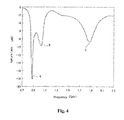
- Fig. 4 is a graph showing a relationship between return loss and frequency in the antenna device shown in Figs. 3A and 3B .
- An antenna device 101 shown in Figs. 3A and 3B is provided with grounding patterns 103 on front and back sides of a board 102.
- a top patch 104 is provided on the front side of the board 102, and this top patch 104 is connected to the grounding pattern 103 on the back side via a through-hole 106 and a line 105.
- a feeding point 107 insulated from the grounding pattern 103 is provided on the front side of the board 102, and a conductive pad 108 extends from this feeding point 107.
- the conductive pad 108 extends from the feeding point 107 to be capacitively coupled with the top patch 104 leaving a predetermined gap therefrom.
- the shape of the top patch 104, the gap distance between the conductive pad 108 and the top patch 104 in capacitive coupling, and the length of the line 105 determine a resonant frequency and a bandwidth on a low frequency side (a side denoted by a reference sign A in Fig. 4 ) of a first-order mode.
- a meander line 109 extends from the middle of the conductive pad 108 in a direction opposite to the top patch 104.
- the meander line 109 is formed by folding back an elongated conductive pad many times. This shape of the meander line 109 determines a resonant frequency and a bandwidth on a high frequency side of a first-order mode (the side denoted by a reference sign B in Fig. 4 ) and those of third-order to fifth-order modes (the third-order mode is denoted by a reference sign C in Fig. 4 ).
- Non-Patent Literature 1 " Small Antennas Based on CRLH Structures", IEEE Antennas and Propagation Magazine, Vol. 53, No. 2, April 2011 .
- this antenna device 101 shown in Figs. 3A and 3B has the following problems.
- adjustment of the resonant frequency on the high frequency side of the first-order mode is performed by changing the length, width, and pitch of the meander line 109, but such a problem is involved that the adjustment is complicated and difficult.
- adjustment of the resonant frequency on the low frequency side of the first-order mode is performed by changing the lengths and shapes of the top patch 104 and the line 105, but the adjustment is also complicated and difficult.
- the present invention has been made in view of the above problems, and an object thereof is to provide an antenna device that can easily adjust the resonant frequency and the bandwidth of the first-order mode and that has a wider bandwidth characteristic of a bandwidth.
- an antenna device wherein a first linear antenna element connected to a grounding pattern and a second linear antenna element connected to a feeding point are capacitively coupled at distal ends thereof, and inductive elements are interposed in respective middle parts of the first linear antenna element and the second linear antenna element.
- linear antenna element means an antenna element including a linear antenna element portion extending unidirectionally and linearly in an elongated fashion.
- the inductive elements be inductors in the form of a chip part.
- the inductive elements may be conductive patterns.
- a third antenna element extends from a middle part of the second linear antenna element.
- the antenna device of the present invention since the first linear antenna element connected to a grounding pattern and the second linear antenna element connected to a feeding point are capacitively coupled at distal ends thereof, resonance on a low frequency side of a first-order mode and resonance on a high frequency side of the first-order mode are capacitively coupled, so that a wider bandwidth characteristic can be obtained than in the case of using only the resonance on the low frequency side. And, since the inductive element is interposed in the middle part of the first linear antenna element, a resonant frequency on the low frequency side of the first-order mode can be adjusted by adjusting the inductance of this inductive element.
- first antenna element and the second antenna element are made linear and have the interposed inductive elements so that the resonant frequency of the first-order mode can be adjusted, it is unnecessary to use a conductive pad having a shape folded back many times, such as a meander line, so that the antenna device can be downsized.
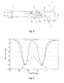
- Fig. 1 is a schematic diagram of the antenna device according to the present invention.
- Fig. 2 is a diagram showing a relationship between return loss and frequency in the antenna device shown in Fig. 1 .
- the antenna device 1 shown in Fig. 1 is used in a wireless communication device, such as a mobile phone, a smartphone, or a tablet computer, and provided with a grounding pattern 2 on a board (not shown).
- a first linear antenna element 3 is connected to the grounding pattern 2.
- This first linear antenna element 3 is provided with a first linear antenna element portion 3a and a second linear antenna element portion 3b.
- the first linear antenna element portion 3a extends unidirectionally (upward in Fig. 1 ) and linearly in a thick and short fashion from the grounding pattern 2.
- the second linear antenna element portion 3b extends linearly in an elongated fashion in a direction orthogonal to the first linear antenna element portion 3a (leftward in Fig. 1 ) from a distal end of the first linear antenna element portion 3a.
- a feeding point 4 insulated from the grounding pattern 2 is provided on the board.
- a second linear antenna element 5 is connected to this feeding point 4.
- the second linear antenna element 5 is provided with a first linear antenna element portion 5a and a second linear antenna element portion 5b.
- the first linear antenna element portion 5a extends unidirectionally (upward in Fig. 1 ) and linearly in a thick and short fashion from the feeding point 4.
- the second linear antenna element portion 5b extends linearly in an elongated fashion in a direction orthogonal to the first linear antenna element portion 5a (leftward in Fig. 1 ) from a distal end of the first linear antenna element portion 5 a.
- the first linear antenna element 3 and the second linear antenna element 5 are capacitively coupled at a capacitive coupling portion 7 at their distal ends thereof.
- a rectangular capacitive coupling portion 3c wider than the second linear antenna element portion 3b is provided at a distal end of the second linear antenna element portion 3b of the first linear antenna element 3.
- a rectangular capacitive coupling portion 5c wider than the second linear antenna element portion 5b is provided at a distal end of the second linear antenna element portion 5b of the second linear antenna element 5. Only one side of the rectangular capacitive coupling portion 3c provided to the first linear antenna element 3 and only one side of the rectangular capacitive coupling portion 5c provided to the second linear antenna element 5 are disposed so as to face each other with a predetermined gap therebetween.
- the first linear antenna element 3 connected to the grounding pattern 2 and the second linear antenna element 5 connected to the feeding point 4 are capacitively coupled at their distal ends. Therefore, resonance on a low frequency side of a first-order mode (a solid line denoted by a reference sign A in Fig. 2 ) and resonance on a high frequency side of the first-order mode (a solid line denoted by a reference sign B in Fig. 2 ) are capacitively coupled. Thereby, a wider bandwidth characteristic (characteristic denoted by a broken line in Fig. 2 ) of a bandwidth can be obtained than in the case of using only resonance on the low frequency side (the case of using only the solid line denoted by the reference sign A in Fig. 2 ).
- an inductive element L1 is interposed in a middle part of the first linear antenna element 3, i.e., at an end on the first linear antenna element portion 3a side of the second linear antenna element portion 3b. It is preferred that the inductive element L1 be provided at a distance of about one-fifth of the entire length of the first linear antenna element 3 from the grounding pattern 2. Further, an inductive element L2 is interposed in a middle part of the second linear antenna element 5, i.e., in a middle portion of the second linear antenna element portion 5b. It is preferred that the inductive element L2 be provided in the vicinity of the center of the entire length of the second linear antenna element 5.
- These inductive elements L1, L2 can be formed of inductors in the form of a chip part or conductive pattern.
- the inductance of the inductive element L1 determines a resonant frequency and a bandwidth on the low frequency side (a side denoted by the reference sign A in Fig. 2 ) of the first-order mode.
- the resonant frequency on the low frequency side of the first-order mode can be adjusted by adjusting the inductance of the inductive element L1 interposed in the middle part of the first linear antenna element 3.
- the resonant frequency and bandwidth on the low frequency side of the first-order mode can be easily adjusted.
- the inductance of the inductive element L2 and the length of the second linear antenna element 5 determine a resonant frequency and a bandwidth on the high frequency side (a side denoted by the reference sign B in Fig. 2 ) of the first-order mode and those of the third-order to fifth-order modes (not shown).
- the resonant frequency on the high frequency side of the first-order mode and those of the third-order to fifth-order modes can be adjusted by adjusting the inductance of the inductive element L2 interposed in the middle part of the second linear antenna element 5.
- the resonant frequency and bandwidth on the high frequency side of the first-order mode and those of the third-order to fifth-order modes can be easily adjusted.
- the resonant frequency on the high frequency side of the first-order mode and those of the third-order to fifth-order modes can be lowered to desired resonant frequencies by adjusting the inductance of the inductive element L2.
- the first antenna element 3 and the second antenna element 5 are made linear and the inductive elements L1 and L2 are interposed in these antenna elements 3 and 5, respectively, so that the resonant frequencies of the first-order mode and the third-order to fifth-order modes can be adjusted.
- the antenna device since a conductive pad having a shape folded many times, such as the conventional meander line 109, is not used, the antenna device can be downsized.
- a third antenna element 6 extends from a middle part of the second linear antenna element 5, i.e., from a position between the feeding point 4 and the inductive element L2 in the second linear antenna element portion 5b. It is preferred that the third antenna element 6 extend from a position of one-fourth ⁇ of the third-order mode of the second linear antenna element 5 from the feeding point 4.
- This third antenna element 6 is provided with a first linear portion 6a extending linearly unidirectionally (upward in Fig. 1 ) from the second linear antenna element portion 5b of the second linear antenna element 5.
- the third antenna element 6 is provided with a second linear portion 6b extending linearly in an elongated fashion in a direction orthogonal to the first linear portion 6a (leftward in Fig. 1 ) from a distal end of the first linear portion 6a. Further, the third antenna element 6 is provided with a third linear portion 6c extending linearly unidirectionally (upward in Fig. 1 ) from a distal end of the second linear portion 6b. Moreover, the third antenna element 6 is provided with a fourth linear portion 6d extending linearly in a direction orthogonal to the third linear portion 6c (leftward in Fig. 1 ) from a distal end of the third linear portion 6c. By providing the third linear portion 6c and the fourth linear portion 6d, the third antenna element 6 is prevented from coming into contact with the inductive element L2.
- the resonant frequencies and bandwidths of the third-order to fifth-order modes can be adjusted independently without affecting the first-order mode.
- the resonant frequencies of the third-order to fifth-order modes can be lowered to desired resonant frequencies by adjusting the length or shape of the third antenna element 6.
- the top patch 104 is formed in a rectangular shape
- the conductive pad 108 is formed in a substantially-L shape so as to face the top patch 104 at a corner of the top patch 104.
- one side of the top patch 104 and one side of the conductive pad 108 face each other, and another side orthogonal to the one side of the top patch 104 and another side orthogonal to the one side of the conductive pad 108 face each other. Therefore, a region required for capacitive coupling is large, and capacitance adjustment is complicated.
- the first linear antenna element 3 only needs to be formed linearly, and is not necessarily limited to one provided with the first linear antenna element portion 3a and the second linear antenna element portion 3b.
- the second linear antenna element 5 only needs to be formed linearly, and is not necessarily limited to one provided with the first linear antenna element portion 5a and the second linear antenna element portion 5b.
- the "linear antenna element" of the first linear antenna element 3 and the second linear antenna element 5 means an antenna element including a linear antenna element portion extending unidirectionally and linearly in an elongated fashion.
- the inductive elements L1, L2 only need to be interposed in the respective middle parts of the first linear antenna element and the second linear antenna element, and are not limited to the example shown in Fig. 1 .
Landscapes
- Variable-Direction Aerials And Aerial Arrays (AREA)
- Support Of Aerials (AREA)
- Details Of Aerials (AREA)
Abstract
Description
- The present invention relates to an antenna device having a wide bandwidth characteristic of a bandwidth used for a wireless communication device, such as a mobile phone, a smartphone, or a tablet computer.
- Conventionally, as an antenna device capable of a wide bandwidth characteristic of a bandwidth, an antenna device based on a CRLH (composite right- and left-hand) structure has been suggested (see a Non-Patent Literature 1).
- An antenna device based on the CRLH structure has a structure shown in
Fig. 3 , for example.Figs. 3A and 3B show a conventional antenna device based on the CRLH structure,Fig. 3A showing a plan view of the antenna device, andFig. 3B showing a bottom view thereof.Fig. 4 is a graph showing a relationship between return loss and frequency in the antenna device shown inFigs. 3A and 3B . - An
antenna device 101 shown inFigs. 3A and 3B is provided withgrounding patterns 103 on front and back sides of aboard 102. Atop patch 104 is provided on the front side of theboard 102, and thistop patch 104 is connected to thegrounding pattern 103 on the back side via a through-hole 106 and aline 105. Further, afeeding point 107 insulated from thegrounding pattern 103 is provided on the front side of theboard 102, and aconductive pad 108 extends from thisfeeding point 107. Theconductive pad 108 extends from thefeeding point 107 to be capacitively coupled with thetop patch 104 leaving a predetermined gap therefrom. The shape of thetop patch 104, the gap distance between theconductive pad 108 and thetop patch 104 in capacitive coupling, and the length of theline 105 determine a resonant frequency and a bandwidth on a low frequency side (a side denoted by a reference sign A inFig. 4 ) of a first-order mode. - On the other hand, on the front side of the
board 102, ameander line 109 extends from the middle of theconductive pad 108 in a direction opposite to thetop patch 104. Themeander line 109 is formed by folding back an elongated conductive pad many times. This shape of themeander line 109 determines a resonant frequency and a bandwidth on a high frequency side of a first-order mode (the side denoted by a reference sign B inFig. 4 ) and those of third-order to fifth-order modes (the third-order mode is denoted by a reference sign C inFig. 4 ). - By capacitively-coupling resonance on the low frequency side of the first-order mode and resonance on the high frequency side of the first-order mode, a wider bandwidth characteristic of a bandwidth can be obtained than in the case of using only resonance on the low frequency side.
- Non-Patent Literature 1: "Small Antennas Based on CRLH Structures", IEEE Antennas and Propagation Magazine, Vol. 53, No. 2, April 2011.
- However, this
antenna device 101 shown inFigs. 3A and 3B has the following problems. - That is, adjustment of the resonant frequency on the high frequency side of the first-order mode is performed by changing the length, width, and pitch of the
meander line 109, but such a problem is involved that the adjustment is complicated and difficult. Similarly, adjustment of the resonant frequency on the low frequency side of the first-order mode is performed by changing the lengths and shapes of thetop patch 104 and theline 105, but the adjustment is also complicated and difficult. - Further, adjustment of the bandwidth on the high frequency side of the first-order mode is performed by changing the width and pitch of the
meander line 109, but the adjustment is also complicated and difficult. - Similarly, adjustment of the bandwidth on the low frequency side of the first-order mode is performed by changing the shape of the
top patch 104 and the line width of theline 105, but the adjustment is also complicated and difficult. - In addition, adjustment of the capacitive coupling of the first-order mode is performed by changing the interval between the
conductive pad 108 and thetop patch 104, but the adjustment is also complicated and difficult. - Therefore, the present invention has been made in view of the above problems, and an object thereof is to provide an antenna device that can easily adjust the resonant frequency and the bandwidth of the first-order mode and that has a wider bandwidth characteristic of a bandwidth.
- According to an aspect of the present invention, there is provided an antenna device wherein a first linear antenna element connected to a grounding pattern and a second linear antenna element connected to a feeding point are capacitively coupled at distal ends thereof, and inductive elements are interposed in respective middle parts of the first linear antenna element and the second linear antenna element.
- The phrase "linear antenna element" means an antenna element including a linear antenna element portion extending unidirectionally and linearly in an elongated fashion.
- In addition, in this antenna device, it is preferred that the inductive elements be inductors in the form of a chip part.
- Further, in this antenna device, the inductive elements may be conductive patterns.
- Also, in this antenna device, it is preferred that a third antenna element extends from a middle part of the second linear antenna element.
- According to the antenna device of the present invention, since the first linear antenna element connected to a grounding pattern and the second linear antenna element connected to a feeding point are capacitively coupled at distal ends thereof, resonance on a low frequency side of a first-order mode and resonance on a high frequency side of the first-order mode are capacitively coupled, so that a wider bandwidth characteristic can be obtained than in the case of using only the resonance on the low frequency side. And, since the inductive element is interposed in the middle part of the first linear antenna element, a resonant frequency on the low frequency side of the first-order mode can be adjusted by adjusting the inductance of this inductive element. In this regard, unlike conventional techniques, such adjustment as changing the shape of a top patch or the length and width of a line is not required, and the resonant frequency and bandwidth on the low frequency side of the first-order mode can be easily adjusted. Similarly, since the inductive element is interposed in the middle part of the second linear antenna element, a resonant frequency on the high frequency side of the first-order mode can be adjusted by adjusting the inductance of this inductive element. In this regard, unlike the conventional techniques, such adjustment as changing the shape or the like of a meander line is not required.
- Further, since the first antenna element and the second antenna element are made linear and have the interposed inductive elements so that the resonant frequency of the first-order mode can be adjusted, it is unnecessary to use a conductive pad having a shape folded back many times, such as a meander line, so that the antenna device can be downsized.
-
-
Fig. 1 is a schematic diagram of an antenna device according to the present invention; -
Fig. 2 is a diagram showing a relationship between return loss and frequency in the antenna device shown inFig. 1 ; -
Figs. 3A and 3B show a conventional antenna device based on a CRLH structure,Fig. 3A showing a plan view of the antenna device andFig. 3B showing a bottom view thereof; and -
Fig. 4 is a graph showing a relationship between return loss and frequency in the antenna device shown inFigs. 3A and 3B . - An embodiment of an antenna device of the present invention will be described below with reference to the drawings.
Fig. 1 is a schematic diagram of the antenna device according to the present invention.Fig. 2 is a diagram showing a relationship between return loss and frequency in the antenna device shown inFig. 1 . - The antenna device 1 shown in
Fig. 1 is used in a wireless communication device, such as a mobile phone, a smartphone, or a tablet computer, and provided with agrounding pattern 2 on a board (not shown). A firstlinear antenna element 3 is connected to thegrounding pattern 2. This firstlinear antenna element 3 is provided with a first linearantenna element portion 3a and a second linearantenna element portion 3b. The first linearantenna element portion 3a extends unidirectionally (upward inFig. 1 ) and linearly in a thick and short fashion from thegrounding pattern 2. The second linearantenna element portion 3b extends linearly in an elongated fashion in a direction orthogonal to the first linearantenna element portion 3a (leftward inFig. 1 ) from a distal end of the first linearantenna element portion 3a. - Also, a
feeding point 4 insulated from thegrounding pattern 2 is provided on the board. A secondlinear antenna element 5 is connected to thisfeeding point 4. The secondlinear antenna element 5 is provided with a first linear antenna element portion 5a and a second linearantenna element portion 5b. The first linear antenna element portion 5a extends unidirectionally (upward inFig. 1 ) and linearly in a thick and short fashion from thefeeding point 4. The second linearantenna element portion 5b extends linearly in an elongated fashion in a direction orthogonal to the first linear antenna element portion 5a (leftward inFig. 1 ) from a distal end of the first linear antenna element portion 5 a. - The first
linear antenna element 3 and the secondlinear antenna element 5 are capacitively coupled at acapacitive coupling portion 7 at their distal ends thereof. Specifically, a rectangularcapacitive coupling portion 3c wider than the second linearantenna element portion 3b is provided at a distal end of the second linearantenna element portion 3b of the firstlinear antenna element 3. Similarly, a rectangularcapacitive coupling portion 5c wider than the second linearantenna element portion 5b is provided at a distal end of the second linearantenna element portion 5b of the secondlinear antenna element 5. Only one side of the rectangularcapacitive coupling portion 3c provided to the firstlinear antenna element 3 and only one side of the rectangularcapacitive coupling portion 5c provided to the secondlinear antenna element 5 are disposed so as to face each other with a predetermined gap therebetween. - Thus, the first
linear antenna element 3 connected to thegrounding pattern 2 and the secondlinear antenna element 5 connected to thefeeding point 4 are capacitively coupled at their distal ends. Therefore, resonance on a low frequency side of a first-order mode (a solid line denoted by a reference sign A inFig. 2 ) and resonance on a high frequency side of the first-order mode (a solid line denoted by a reference sign B inFig. 2 ) are capacitively coupled. Thereby, a wider bandwidth characteristic (characteristic denoted by a broken line inFig. 2 ) of a bandwidth can be obtained than in the case of using only resonance on the low frequency side (the case of using only the solid line denoted by the reference sign A inFig. 2 ). - In addition, an inductive element L1 is interposed in a middle part of the first
linear antenna element 3, i.e., at an end on the first linearantenna element portion 3a side of the second linearantenna element portion 3b. It is preferred that the inductive element L1 be provided at a distance of about one-fifth of the entire length of the firstlinear antenna element 3 from thegrounding pattern 2. Further, an inductive element L2 is interposed in a middle part of the secondlinear antenna element 5, i.e., in a middle portion of the second linearantenna element portion 5b. It is preferred that the inductive element L2 be provided in the vicinity of the center of the entire length of the secondlinear antenna element 5. These inductive elements L1, L2 can be formed of inductors in the form of a chip part or conductive pattern. - Here, the inductance of the inductive element L1, the gap distance between the rectangular
capacitive coupling portions linear antenna element 3 determine a resonant frequency and a bandwidth on the low frequency side (a side denoted by the reference sign A inFig. 2 ) of the first-order mode. - Therefore, the resonant frequency on the low frequency side of the first-order mode can be adjusted by adjusting the inductance of the inductive element L1 interposed in the middle part of the first
linear antenna element 3. In this regard, unlike conventional techniques, without requiring such adjustment as changing the shape of a top patch or the length and width of a line, the resonant frequency and bandwidth on the low frequency side of the first-order mode can be easily adjusted. - Further, the inductance of the inductive element L2 and the length of the second
linear antenna element 5 determine a resonant frequency and a bandwidth on the high frequency side (a side denoted by the reference sign B inFig. 2 ) of the first-order mode and those of the third-order to fifth-order modes (not shown). - Therefore, the resonant frequency on the high frequency side of the first-order mode and those of the third-order to fifth-order modes can be adjusted by adjusting the inductance of the inductive element L2 interposed in the middle part of the second
linear antenna element 5. In this regard, unlike conventional techniques, without requiring such adjustment as changing the length, width, and pitch of a meander line, the resonant frequency and bandwidth on the high frequency side of the first-order mode and those of the third-order to fifth-order modes can be easily adjusted. In particular, the resonant frequency on the high frequency side of the first-order mode and those of the third-order to fifth-order modes can be lowered to desired resonant frequencies by adjusting the inductance of the inductive element L2. - In addition, the
first antenna element 3 and thesecond antenna element 5 are made linear and the inductive elements L1 and L2 are interposed in theseantenna elements conventional meander line 109, is not used, the antenna device can be downsized. - Further, in the antenna device 1, as shown in
Fig. 1 , athird antenna element 6 extends from a middle part of the secondlinear antenna element 5, i.e., from a position between thefeeding point 4 and the inductive element L2 in the second linearantenna element portion 5b. It is preferred that thethird antenna element 6 extend from a position of one-fourth λ of the third-order mode of the secondlinear antenna element 5 from thefeeding point 4. Thisthird antenna element 6 is provided with a firstlinear portion 6a extending linearly unidirectionally (upward inFig. 1 ) from the second linearantenna element portion 5b of the secondlinear antenna element 5. Further, thethird antenna element 6 is provided with a secondlinear portion 6b extending linearly in an elongated fashion in a direction orthogonal to the firstlinear portion 6a (leftward inFig. 1 ) from a distal end of the firstlinear portion 6a. Further, thethird antenna element 6 is provided with a thirdlinear portion 6c extending linearly unidirectionally (upward inFig. 1 ) from a distal end of the secondlinear portion 6b. Moreover, thethird antenna element 6 is provided with a fourthlinear portion 6d extending linearly in a direction orthogonal to the thirdlinear portion 6c (leftward inFig. 1 ) from a distal end of the thirdlinear portion 6c. By providing the thirdlinear portion 6c and the fourthlinear portion 6d, thethird antenna element 6 is prevented from coming into contact with the inductive element L2. - By adjusting the length or shape of the
third antenna element 6, the resonant frequencies and bandwidths of the third-order to fifth-order modes can be adjusted independently without affecting the first-order mode. In particular, the resonant frequencies of the third-order to fifth-order modes can be lowered to desired resonant frequencies by adjusting the length or shape of thethird antenna element 6. - It should be noted that in the
capacitive coupling portion 7 between the firstlinear antenna element 3 and the secondlinear antenna element 5, only one side of the rectangularcapacitive coupling portion 3c on the firstlinear antenna element 3 side and only one side of the rectangularcapacitive coupling portion 5c on the secondlinear antenna element 5 side are disposed so as to face each other with a predetermined gap therebetween. Therefore, a region required for capacitive coupling is small, so that capacitance can be adjusted only by adjusting the gap distance between and facing lengths of the one side of the rectangularcapacitive coupling portion 3c and the one side of the rectangularcapacitive coupling portion 5c facing each other. In contrast, in the capacitive coupling portion of theconventional antenna device 101 shown inFig. 3 , thetop patch 104 is formed in a rectangular shape, and theconductive pad 108 is formed in a substantially-L shape so as to face thetop patch 104 at a corner of thetop patch 104. Thus, one side of thetop patch 104 and one side of theconductive pad 108 face each other, and another side orthogonal to the one side of thetop patch 104 and another side orthogonal to the one side of theconductive pad 108 face each other. Therefore, a region required for capacitive coupling is large, and capacitance adjustment is complicated. - The embodiment of the preset invention has been described above, but the present invention is not limited to the embodiment, and can be altered or modified variously.
- For example, the first
linear antenna element 3 only needs to be formed linearly, and is not necessarily limited to one provided with the first linearantenna element portion 3a and the second linearantenna element portion 3b. - Similarly, the second
linear antenna element 5 only needs to be formed linearly, and is not necessarily limited to one provided with the first linear antenna element portion 5a and the second linearantenna element portion 5b. In this regard, the "linear antenna element" of the firstlinear antenna element 3 and the secondlinear antenna element 5 means an antenna element including a linear antenna element portion extending unidirectionally and linearly in an elongated fashion. - Further, the inductive elements L1, L2 only need to be interposed in the respective middle parts of the first linear antenna element and the second linear antenna element, and are not limited to the example shown in
Fig. 1 .
Claims (11)
- An antenna device (1) wherein a first linear antenna element (3) connected to a grounding pattern (2) and a second linear antenna element (5) connected to a feeding point (4) are capacitively coupled at distal ends (3c, 5c) thereof, and inductive elements (L1, L2) are interposed in respective middle parts of the first linear antenna element (3) and the second linear antenna element (5).
- The antenna device according to claim 1, wherein the inductive elements (L1, L2) are inductors in the form of a chip part.
- The antenna device according to claim 1, wherein the inductive elements (L1, L2) are conductive patterns.
- The antenna device according to any one of claims 1 to 3, wherein a third antenna element (6) extends from a middle part of the second linear antenna element (5).
- The antenna device according to claim 4, wherein the third antenna element (6) extends between the first linear antenna element (3) and the second linear antenna element (5).
- The antenna device according to claim 4 or 5, wherein the third antenna element (6) extends from the second linear antenna element (5) at a position between the feeding point (4) and the inductive element (L2).
- The antenna device according to any preceding claim, wherein the first linear antenna element (3) comprises a first linear antenna element portion (3a) and a second linear antenna element portion (3b) that extends orthogonal to the first linear antenna element portion (3a) from a distal end of the first linear antenna element portion (3a).
- The antenna device according to any preceding claim, wherein the second linear antenna element (5) comprises a first linear antenna element portion (5a) and a second linear antenna element portion (5b) that extends orthogonal to the first linear antenna element portion (5a) of the second linear antenna element (5) and from a distal end of the first linear antenna element portion (5a) of the second linear antenna element (5).
- The antenna device according to claim 8 when appended to claim 7, wherein the second linear antenna element portion (3b) of the first linear antenna element (3) is parallel to the second linear antenna element portion (5b) of the second linear antenna element (5).
- The antenna device according to claim 9 or claim 8 when appended to claim 7, wherein a rectangular capacitive coupling portion (3c) wider than the second linear antenna element portion (3b) is provided at a distal end of the second linear antenna element portion (3b) of the first linear antenna element (3), and wherein a rectangular capacitive coupling portion (5c) wider than the second linear antenna element portion (5b) is provided at a distal end of the second linear antenna element portion (5b) of the second linear antenna element (5).
- The antenna device according to claim 10, wherein the rectangular capacitive coupling portion (3c) of the first linear antenna element (3) is disposed to face the rectangular capacitive coupling portion (5c) ofthe second linear antenna element (5) along only one side of the rectangular capacitive coupling portion (3c) of the first linear antenna element (3).
Applications Claiming Priority (1)
| Application Number | Priority Date | Filing Date | Title |
|---|---|---|---|
| JP2013003216A JP2014135664A (en) | 2013-01-11 | 2013-01-11 | Antenna device |
Publications (1)
| Publication Number | Publication Date |
|---|---|
| EP2755278A1 true EP2755278A1 (en) | 2014-07-16 |
Family
ID=49885171
Family Applications (1)
| Application Number | Title | Priority Date | Filing Date |
|---|---|---|---|
| EP14150419.1A Withdrawn EP2755278A1 (en) | 2013-01-11 | 2014-01-08 | Antenna device |
Country Status (6)
| Country | Link |
|---|---|
| US (1) | US9831555B2 (en) |
| EP (1) | EP2755278A1 (en) |
| JP (1) | JP2014135664A (en) |
| KR (1) | KR20140091450A (en) |
| CN (1) | CN103928749A (en) |
| TW (1) | TWM464834U (en) |
Families Citing this family (3)
| Publication number | Priority date | Publication date | Assignee | Title |
|---|---|---|---|---|
| KR102364470B1 (en) | 2017-08-23 | 2022-02-18 | 삼성전자주식회사 | Electronic device comprising antenna |
| CN109980364B (en) * | 2019-02-28 | 2021-09-14 | 华为技术有限公司 | Antenna module, antenna device and terminal equipment |
| CN118841754B (en) * | 2024-09-20 | 2024-12-10 | 微网优联科技(成都)有限公司 | High-gain omnidirectional dip antenna |
Citations (5)
| Publication number | Priority date | Publication date | Assignee | Title |
|---|---|---|---|---|
| WO2004025778A1 (en) * | 2002-09-10 | 2004-03-25 | Fractus, S.A. | Coupled multiband antennas |
| EP1608035A1 (en) * | 2004-06-14 | 2005-12-21 | Nec Corporation | Antenna device and portable radio terminal |
| EP2418728A1 (en) * | 2010-08-09 | 2012-02-15 | Sony Ericsson Mobile Communications AB | Antenna arrangement, dielectric substrate, PCB & device |
| US20120162036A1 (en) * | 2010-12-28 | 2012-06-28 | Fujitsu Component Limited | Antenna device |
| EP2562871A1 (en) * | 2011-08-25 | 2013-02-27 | Samsung Electronics Co., Ltd. | Antenna apparatus of mobile terminal |
Family Cites Families (16)
| Publication number | Priority date | Publication date | Assignee | Title |
|---|---|---|---|---|
| SE514530C2 (en) * | 1998-05-18 | 2001-03-12 | Allgon Ab | An antenna device comprising capacitively coupled radio tower elements and a hand-held radio communication device for such an antenna device |
| US6081242A (en) * | 1998-06-16 | 2000-06-27 | Galtronics U.S.A., Inc. | Antenna matching circuit |
| JP2001185938A (en) | 1999-12-27 | 2001-07-06 | Mitsubishi Electric Corp | Dual-frequency antenna, multi-frequency antenna, and dual-frequency or multi-frequency array antenna |
| US6650294B2 (en) * | 2001-11-26 | 2003-11-18 | Telefonaktiebolaget Lm Ericsson (Publ) | Compact broadband antenna |
| JP2005020228A (en) | 2003-06-25 | 2005-01-20 | Sony Ericsson Mobilecommunications Japan Inc | Antenna equipment |
| CN1716688A (en) * | 2004-06-14 | 2006-01-04 | 日本电气株式会社 | Antenna equipment and portable radio terminal |
| US7423598B2 (en) * | 2006-12-06 | 2008-09-09 | Motorola, Inc. | Communication device with a wideband antenna |
| JP5009240B2 (en) * | 2008-06-25 | 2012-08-22 | ソニーモバイルコミュニケーションズ株式会社 | Multiband antenna and wireless communication terminal |
| JP2010245894A (en) * | 2009-04-07 | 2010-10-28 | Murata Mfg Co Ltd | Antenna and radio communication equipment |
| WO2010137061A1 (en) * | 2009-05-26 | 2010-12-02 | 株式会社 東芝 | Antenna device |
| TWI431849B (en) * | 2009-11-24 | 2014-03-21 | Ind Tech Res Inst | Mobile communication device |
| US8354967B2 (en) * | 2010-05-11 | 2013-01-15 | Sony Ericsson Mobile Communications Ab | Antenna array with capacitive coupled upper and lower antenna elements and a peak radiation pattern directed toward the lower antenna element |
| TWI451631B (en) * | 2010-07-02 | 2014-09-01 | Ind Tech Res Inst | Multiband antenna and method for an antenna to be capable of multiband operation |
| TWI508373B (en) * | 2011-04-27 | 2015-11-11 | Chiun Mai Comm Systems Inc | Multiband antenna |
| EP2774216B1 (en) * | 2011-11-04 | 2021-05-05 | Dockon AG | Capacitively coupled compound loop antenna |
| US9496614B2 (en) * | 2014-04-15 | 2016-11-15 | Dockon Ag | Antenna system using capacitively coupled compound loop antennas with antenna isolation provision |
-
2013
- 2013-01-11 JP JP2013003216A patent/JP2014135664A/en active Pending
- 2013-05-27 TW TW102209826U patent/TWM464834U/en not_active IP Right Cessation
- 2013-12-26 KR KR1020130163952A patent/KR20140091450A/en not_active Withdrawn
-
2014
- 2014-01-08 EP EP14150419.1A patent/EP2755278A1/en not_active Withdrawn
- 2014-01-10 CN CN201410011575.3A patent/CN103928749A/en active Pending
- 2014-01-13 US US14/153,599 patent/US9831555B2/en active Active
Patent Citations (5)
| Publication number | Priority date | Publication date | Assignee | Title |
|---|---|---|---|---|
| WO2004025778A1 (en) * | 2002-09-10 | 2004-03-25 | Fractus, S.A. | Coupled multiband antennas |
| EP1608035A1 (en) * | 2004-06-14 | 2005-12-21 | Nec Corporation | Antenna device and portable radio terminal |
| EP2418728A1 (en) * | 2010-08-09 | 2012-02-15 | Sony Ericsson Mobile Communications AB | Antenna arrangement, dielectric substrate, PCB & device |
| US20120162036A1 (en) * | 2010-12-28 | 2012-06-28 | Fujitsu Component Limited | Antenna device |
| EP2562871A1 (en) * | 2011-08-25 | 2013-02-27 | Samsung Electronics Co., Ltd. | Antenna apparatus of mobile terminal |
Non-Patent Citations (1)
| Title |
|---|
| "Small Antennas Based on CRLH Structures", IEEE ANTENNAS AND PROPAGATION MAGAZINE, vol. 53, no. 2, April 2011 (2011-04-01) |
Also Published As
| Publication number | Publication date |
|---|---|
| JP2014135664A (en) | 2014-07-24 |
| CN103928749A (en) | 2014-07-16 |
| US9831555B2 (en) | 2017-11-28 |
| KR20140091450A (en) | 2014-07-21 |
| TWM464834U (en) | 2013-11-01 |
| US20140198003A1 (en) | 2014-07-17 |
Similar Documents
| Publication | Publication Date | Title |
|---|---|---|
| CN101147294B (en) | Antennas with multiple resonant frequencies | |
| US8779985B2 (en) | Dual radiator monopole antenna | |
| TWI549368B (en) | Communication device | |
| US9391371B2 (en) | Antenna device and wireless communication device using the same | |
| JP5998974B2 (en) | antenna | |
| US8643549B2 (en) | Multi-resonant antenna | |
| US20130135154A1 (en) | Portable wireless device | |
| US20180131075A1 (en) | Mobile device | |
| US9590303B2 (en) | Antenna | |
| CN103299483B (en) | Substrate for antenna device and antenna device | |
| KR101842627B1 (en) | Frequency tunable device, antenna, electromagnetic wave absorber including the same, and method for extending operating frequency of the same | |
| EP2755278A1 (en) | Antenna device | |
| KR100626667B1 (en) | Planar Inverted F Antenna | |
| TWI524595B (en) | Antenna | |
| US20110279348A1 (en) | Antenna device | |
| TWI524589B (en) | Low impedance slot fed antenna | |
| JP2012253641A (en) | Antenna device | |
| US20170064052A1 (en) | Communication device | |
| US9923262B2 (en) | Mobile device | |
| JP6548112B2 (en) | Broadband antenna | |
| JP2013150101A (en) | Antenna | |
| US20170170543A1 (en) | Antenna and electric device using the same | |
| US20140292585A1 (en) | Antenna and wireless communication device | |
| CN112290208A (en) | Antenna | |
| JP4241539B2 (en) | Surface mount type antenna and radio communication apparatus including the same |
Legal Events
| Date | Code | Title | Description |
|---|---|---|---|
| PUAI | Public reference made under article 153(3) epc to a published international application that has entered the european phase |
Free format text: ORIGINAL CODE: 0009012 |
|
| 17P | Request for examination filed |
Effective date: 20140108 |
|
| AK | Designated contracting states |
Kind code of ref document: A1 Designated state(s): AL AT BE BG CH CY CZ DE DK EE ES FI FR GB GR HR HU IE IS IT LI LT LU LV MC MK MT NL NO PL PT RO RS SE SI SK SM TR |
|
| AX | Request for extension of the european patent |
Extension state: BA ME |
|
| R17P | Request for examination filed (corrected) |
Effective date: 20141217 |
|
| RBV | Designated contracting states (corrected) |
Designated state(s): AL AT BE BG CH CY CZ DE DK EE ES FI FR GB GR HR HU IE IS IT LI LT LU LV MC MK MT NL NO PL PT RO RS SE SI SK SM TR |
|
| STAA | Information on the status of an ep patent application or granted ep patent |
Free format text: STATUS: THE APPLICATION HAS BEEN WITHDRAWN |
|
| 18W | Application withdrawn |
Effective date: 20170309 |