EP2755208A1 - Multiport memory with matching address and data line control - Google Patents
Multiport memory with matching address and data line control Download PDFInfo
- Publication number
- EP2755208A1 EP2755208A1 EP14150651.9A EP14150651A EP2755208A1 EP 2755208 A1 EP2755208 A1 EP 2755208A1 EP 14150651 A EP14150651 A EP 14150651A EP 2755208 A1 EP2755208 A1 EP 2755208A1
- Authority
- EP
- European Patent Office
- Prior art keywords
- line pair
- read
- match
- bit
- port
- Prior art date
- Legal status (The legal status is an assumption and is not a legal conclusion. Google has not performed a legal analysis and makes no representation as to the accuracy of the status listed.)
- Granted
Links
- 230000015654 memory Effects 0.000 title description 50
- 230000004044 response Effects 0.000 claims description 19
- 238000000034 method Methods 0.000 claims description 15
- 230000003068 static effect Effects 0.000 claims description 5
- 230000000295 complement effect Effects 0.000 description 44
- 239000000872 buffer Substances 0.000 description 38
- 238000012512 characterization method Methods 0.000 description 16
- 238000010586 diagram Methods 0.000 description 5
- 230000008901 benefit Effects 0.000 description 3
- 230000008878 coupling Effects 0.000 description 3
- 238000010168 coupling process Methods 0.000 description 3
- 238000005859 coupling reaction Methods 0.000 description 3
- 239000004065 semiconductor Substances 0.000 description 3
- 238000012986 modification Methods 0.000 description 2
- 230000004048 modification Effects 0.000 description 2
- 230000002411 adverse Effects 0.000 description 1
- 230000003139 buffering effect Effects 0.000 description 1
- 230000008859 change Effects 0.000 description 1
- 230000000694 effects Effects 0.000 description 1
- 238000005516 engineering process Methods 0.000 description 1
- 230000003116 impacting effect Effects 0.000 description 1
- 238000012913 prioritisation Methods 0.000 description 1
- 230000002123 temporal effect Effects 0.000 description 1
Images

Classifications
-
- G—PHYSICS
- G11—INFORMATION STORAGE
- G11C—STATIC STORES
- G11C7/00—Arrangements for writing information into, or reading information out from, a digital store
- G11C7/12—Bit line control circuits, e.g. drivers, boosters, pull-up circuits, pull-down circuits, precharging circuits, equalising circuits, for bit lines
-
- G—PHYSICS
- G11—INFORMATION STORAGE
- G11C—STATIC STORES
- G11C8/00—Arrangements for selecting an address in a digital store
- G11C8/16—Multiple access memory array, e.g. addressing one storage element via at least two independent addressing line groups
-
- G—PHYSICS
- G11—INFORMATION STORAGE
- G11C—STATIC STORES
- G11C11/00—Digital stores characterised by the use of particular electric or magnetic storage elements; Storage elements therefor
- G11C11/21—Digital stores characterised by the use of particular electric or magnetic storage elements; Storage elements therefor using electric elements
- G11C11/34—Digital stores characterised by the use of particular electric or magnetic storage elements; Storage elements therefor using electric elements using semiconductor devices
- G11C11/40—Digital stores characterised by the use of particular electric or magnetic storage elements; Storage elements therefor using electric elements using semiconductor devices using transistors
- G11C11/41—Digital stores characterised by the use of particular electric or magnetic storage elements; Storage elements therefor using electric elements using semiconductor devices using transistors forming static cells with positive feedback, i.e. cells not needing refreshing or charge regeneration, e.g. bistable multivibrator or Schmitt trigger
- G11C11/412—Digital stores characterised by the use of particular electric or magnetic storage elements; Storage elements therefor using electric elements using semiconductor devices using transistors forming static cells with positive feedback, i.e. cells not needing refreshing or charge regeneration, e.g. bistable multivibrator or Schmitt trigger using field-effect transistors only
-
- G—PHYSICS
- G11—INFORMATION STORAGE
- G11C—STATIC STORES
- G11C11/00—Digital stores characterised by the use of particular electric or magnetic storage elements; Storage elements therefor
- G11C11/21—Digital stores characterised by the use of particular electric or magnetic storage elements; Storage elements therefor using electric elements
- G11C11/34—Digital stores characterised by the use of particular electric or magnetic storage elements; Storage elements therefor using electric elements using semiconductor devices
- G11C11/40—Digital stores characterised by the use of particular electric or magnetic storage elements; Storage elements therefor using electric elements using semiconductor devices using transistors
- G11C11/41—Digital stores characterised by the use of particular electric or magnetic storage elements; Storage elements therefor using electric elements using semiconductor devices using transistors forming static cells with positive feedback, i.e. cells not needing refreshing or charge regeneration, e.g. bistable multivibrator or Schmitt trigger
- G11C11/413—Auxiliary circuits, e.g. for addressing, decoding, driving, writing, sensing, timing or power reduction
-
- G—PHYSICS
- G11—INFORMATION STORAGE
- G11C—STATIC STORES
- G11C7/00—Arrangements for writing information into, or reading information out from, a digital store
- G11C7/18—Bit line organisation; Bit line lay-out
Definitions
- This disclosure relates generally to semiconductor devices, and more specifically, to multiport semiconductor memory devices.
- Multi-port memories by providing access to the storage element of memory cells to more than one resource, such as in the case of multi-core processor or an interface between a processor and a bus, have become more commonly used.
- One of the issues with multi-port memories is how to coordinate this aspect of providing access to more than one resource. Often this ability is achieved using wait states and/or arbitration. This can result in unpredictable access times which is undesirable.
- bit line pair of one port when a bit cell is selected by two ports, a bit line pair of one port is kept decoupled from the storage nodes of the selected memory cell and from its data line pair whereas the bit line pair of the other port is coupled to the storage nodes of the selected memory cell and to its data line pair and to the data line pair of the one port. Also the selected word line of the one port is kept disabled whereas the selected word line of the other port is enabled. Thus, the capacitance of the bit line pair of the one port is kept from adversely impacting the access to the selected bit cell whereas the bit line pair of the other port provides the needed access. Bit cell stability issues associated with simultaneous multiport access to a common bit cell are thus avoided.
- the bit line pair of the one port is coupled to the data line pair of the one port by column decoding. This is better understood by reference to the drawings and the following description.
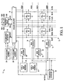
- FIG. 1 Shown in FIG. 1 is a memory 10 having an array 12, a port A row decoder 14, a port B row decoder 16, column circuitry 18, port A row address buffer 20, a port B row address buffer 22, a row match detector 24, a port A column address buffer 26, a port B column address buffer 28, a column match detector 45, and a read/write circuit 100.
- Port A row decoder 14 comprises a row decoder 30 and a row decoder 32.
- Port B row decoder 22 comprises a row decoder 34 and a row decoder 36.
- Array 12 comprises bit cells 38, 40, 42, and 44.
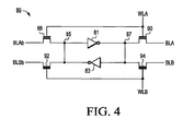
- Bit cell 38 which is a static random access memory (SRAM) cell, comprises inverters 81 and 83 connected to nodes 85 and 87 and transistors 88, 90, 92, and 94 which are N channel transistors in this example.
- Inverter 80 has an input connected to node 85 and an output connected to node 87.
- Inverter 83 has an input connected to node 87 and an output connected node 85.
- Nodes 85 and 87 are storage nodes of memory cell 38.
- Transistor 88 has a first current electrode connected to node 85, a control electrode connected to word line WLA which is a port A word line, and a second current electrode connected to bit line BLAb which is a complementary bit line of port A.
- Transistor 90 has a first current electrode connected to node 87, a control electrode connected to word line WLA, and a second current electrode connected to bit line BLA which is a true bit line of port A.
- Transistor 92 has a first current electrode connected to node 85, a control electrode connected to a word line WLB, which is a word line of port B, and a second current electrode connected to complementary bit line BLBb of port B.
- Memory cells 42 and 44 have a first enable input connected to word line WL1A and a second enable input connected to word line WL1B.
- the access nodes for port A of memory cell 42 are connected to true and complementary bit lines BL0A and BL0Ab and and the access nodes for port B are connected to true and complementary bit lines BL0B and BL0Bb.
- the access nodes for port A of memory cell 44 are connected to true and complementary bit lines BL1A and BL1Ab, and the access nodes for port B are connected to true and complementary bit lines BL1 B and BL1 Bb.
- Port A row address buffer 20 provides true and complementary signals of row address signals for port A.
- Port B row address buffer 22 provides true and complementary signals of row address signals for port B.
- Row decoders 30 and 32 are coupled to the combination of true and complementary address signals for port A. When row decoders 30 and 32 output a logic high, they select word line WL0A and WL1A, respectively. Row decoders 34 and 36 are coupled to the combination of true and complementary address signals for port B. When row decoders 34 and 36 are a logic high, they select word line WL0B and WL1B, respectively. Row match detector 24 is coupled to address buffers 20 and 22 and detects when they provide the same address and provides a true and a complement signals of a row match indicator MATCH R which is coupled to row decoders 34 and 36 that are associated with port B.
- bit lines in both ports coupled to the selected word lines of the corresponding port are activated by the memory cells coupled to the active word lines. That is, in normal operation both ports are active in array 12 so that a word line and bit lines are activated for both ports.
- Column circuitry 18 is coupled to bit lines BL0A, BL0Ab, BL0B, BLBb, BL1A, BL1Ab, BL1B, and BL1 Bb, selects among these bit lines, senses data at the selected bit lines, and couples the sensed data to global data lines GDLA for port A and GDLB for port B in response to column addresses provided by port A column address buffer 26 and port B column address buffer 28.
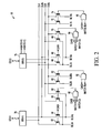
- Column circuitry 18 comprises transistors 52, 54, 56, 58, 60, 62, 64, 66, 68, 70, 72, and 74, a read/write (R/W) A buffer 76 for port A, a R/W B buffer 78 for port B, AND gates 80, 82, 84, and 86.
- Column circuitry 18 less the R/W A buffer 76 and R/W B buffer 78 may be referenced as switching logic.
- Transistor 54 has a first current electrode connected to bit line BL0Ab, a control electrode for receiving column address signal CA0A, and a second current electrode connected to a complementary data line DLAb that is coupled to R/W A buffer 76.
- Transistor 60 has a first current electrode connected to bit line BL0B, a control electrode connected to an output of AND gate 80, and a second current electrode coupled to a true data line DLB for port B that is coupled to R/W B buffer 78 for port B.
- Transistor 62 has a first current electrode connected to bit line BLBb, a control electrode connected to the output of AND gate 82, and a second current electrode coupled to a complementary data line DLBb for port B that is connected to R/W B buffer 78 for port B.
- Transistor 66 has a first current electrode connected to bit line BL1Ab, a control electrode for receiving column address CA1A, and a second current electrode connected to complementary data line DLAb that is coupled to R/W A buffer 76.
- Transistor 72 has a first current electrode connected to bit line BL1B, a control electrode connected to an output of AND gate 86, and a second current electrode coupled to true data line DLB for port B that is connected to R/W B buffer 78 for port B.
- Transistor 74 has a first current electrode coupled to BL1Bb, a control gate coupled to the output of NAND gate 86, and a second current electrode coupled to data line DLBb.
- Transistor 56 has a first current electrode connected to bit line BL0A which is for port A, a control electrode connected to the output of AND gate 80, and a second current electrode coupled to data line DLB which is for port B that is connected to R/W B buffer 78 for port B.
- Transistor 58 has a first current electrode connected to complementary bit line BL0Ab which is for port A, a control electrode connected to the output of AND gate 80, and a second current electrode coupled to complementary data line DLBb which is for port B that is connected to R/W B buffer 78 for port B.
- AND gate 80 has a first input for receiving column address signal CA0B which is for port B, row match indicator match R, and complementary column match indicator MATCH Cb.
- Transistors 56 and 58 are conductive and couple the pair of port A bit lines BL0A and BL0Ab to port B data lines DLB and DLBb so that the port B R/WB circuit may write to or read from the port A bit line pair.
- Transistor 68 has a first current electrode connected to bit line BL1 A which is for port A, a control electrode connected to the output of AND gate 84, and a second current electrode coupled to data line DLB which is for port B that is connected to R/W B buffer 78 for port B.
- Transistor 70 has a first current electrode connected to complementary bit line BL1Ab which is for port A, a control electrode connected to the output of AND gate 84, and a second current electrode coupled to complementary data line DLBb which is for port B that is connected to R/W B buffer 78 for port B.
- AND gate 84 has a first input for receiving column address signal CA1B which is for port B, row match indicator match R, and complementary column match indicator MATCH Cb.
- AND gate 80 when the column addresses for ports A and B match complementary column match indicator MATCH Cb is a logic low thus when there is a column address match, AND gate 84 is forced to provide a logic low output which causes transistors 68 and 70 to be non-conductive.
- row match indictor MATCH R is a logic low which also forces AND gate 84 to provide a logic low.
- the output of AND gate 80 is a logic low and transistors 68 and 70 are non-conductive.
- MATCH R and MATCH Cb are both a logic high so that the output of AND gate 80 follows column address signal CA0B.
- Port B data line pair DLB, DLB0 is coupled to a different bit line pair than the bit line pair accessed by port A and coupled to the data line pair DLA, DLAb. Consequently each addressed bit line pair of port A is coupled to only one data line pair, either DLA, DLAb or DLB, DLBb. As stated before all of the bit lines of port B are disconnected under row address match conditions.
- read/write circuit 100 coupled to global data lines GDLA and GDLB for ports A and B, respectively, comprising read circuitry 102 for port A, write circuitry 104 for port A, read circuitry 106 for port B, and write circuitry 108 for port B.
- Read circuitry 102 has an input coupled to global data lines GDLA and a read output RDA for outputting data that has been read for port A.
- Write circuitry 104 has an output coupled to global data lines GDLA and a write input WDA for receiving data that is to be written for port A.
- Read circuitry 106 has an input coupled to global data lines GDLB and read output RDB for outputting data that has been read for port B.
- Write circuitry 108 has an output coupled to global data lines GDLB and a write input WDB for receiving data that is to be written for port A.
- Read circuitry 102 further has an input coupled to write input WDB, an input for receiving match R, and an input for receiving match C.
- Write circuitry 104 further has an input coupled to write input WDB, an input for receiving match R, and an input for receiving match C.
- Read circuitry 106 further has an input coupled to write input WDA, an input for receiving match R, and an input for receiving match C.
- data present on the bit lines is selectively coupled to data line pair DLA and DLAb and data line pair DLB and DLBb from port A bit lines and port B bit lines, respectively.
- the selection is made by column address signals CA0A and CA1A for port A and column address signals Ca0B and CA1B for port B.
- the row decoder selected by the port A row address enables its word line
- the row decoder selected by the port B address enables its word line.
- MATCH R is not asserted because the row addresses for ports A and B are different so none the row decoders are disabled due to match R.
- R/W A buffer 76 and R/W B buffer 78 each include a sensing circuit and a write driver. For a read, R/W A buffer 76 and R/W B buffer 78 sense the data present on data line pair DLA and DLBb and data line pair DLB and DLBb, respectively.
- the data is provided on global data lines GDLA and GDLB.
- data is received on global data lines GDLA and GDLB.
- the data is then written by R/W A buffer 76 and R/W B buffer 78 onto data line pair DLA and DLAb and data line pair DLB and DLBb, respectively.
- the bit lines are selected for a write in the same manner as for a read. In this example, the selection is a one of two selection.
- the bit line pair associated with a column address is the bit line pair selected for normal operation in which the row addresses for port A and B are different.
- column address CA0A is associated with bit line pair BL0A and BL0Ab
- column address CA1A is associated with bit line pair BL1A and BL1Ab
- column address CA0B is associated with bit line pair BL0B and BLBb
- column address CA1B is associated with bit line pair BL1B and BL1Bb.
- R/W A buffer 76 and R/W B buffer 78 receive the data to be written from global data lines GDLA and GDLB, respectively.
- R/W A buffer 76 writes the received data onto data line pair DLA and DLAb.
- R/W B buffer 78 writes the data onto data line pair DLB and DLBb. Selected columns couple the data on the data lines to their bit lines.
- bit lines BL0A and BL0Ab are to be written for port A
- transistors 52 and 54 are made conductive by column address signal CA0A being asserted at a logic high.
- column address signal CA1B is asserted and transistors 72 and 74 are conductive to provide data onto the selected bit line pair of BL1B and BL1Bb.
- transistors 68 and 70 couple bit line pair BL1 A and BL1Ab, which are port A bit lines, to data lines DLB and DLBb, which are port B data lines.
- bit cell being read or written on port B is read or written by the port B R/W B buffer 78 through port A bit lines, bit line pair BL1A and BL1 b.
- MATCH R being a logic high, the selected port B row decoder is disabled.
- row match detector asserts MATCH R which is received by port B row decoder 34 disabling the port B decoder.
- port B row decoders disabled, then no word lines of port B are enabled with the result that the memory cells along the selected row are coupled to port A bit lines only so that the memory cells along the selected row are subjected to the capacitance of only the port A bit line pair and not the port B bit line pair.
- the port B data is accessed through pass transistors that are connected to the port B data lines and the port A bit line pair line pair of the column selected by the port B address.
- Port A operates normally in that the bit line pair of the column selected by the port A address is coupled to the port A data lines, data lines DLA and DLAb.
- both port A and port B are addressing the same memory cell.
- the access to the port B bit lines is blocked. The only access to the memory cells is through the port A data lines and port A bit lines.
- a write to either port A or Port B is accomplished through write circuitry 104 to GDLA and read/write circuit 76 through data line pair DLA, DLAb and bit line pair BL0A, BL0Ab or BL1A, BI1Ab to the selected memory cell.
- R/W B buffer 78 is not used in case of both ports addressing the same memory cell.
- READ/Write Circuit 100 of FIG. 3 responds in different ways depending on MATCH C, MATCH R, and depending if either port A or port B is writing
- port A reads from or writes through to the global data line GDLA to R/W A circuit 76
- port B reads from or writes to R/W A circuit 78 through global data line GDLB.
- read circuitry A 102 receives the data on global data line GDLA, provides the needed buffering and timing, and provides an output RDA as the output of port A.
- read circuitry B 106 responds to the data provided on global data line GDLA by providing an output RDB for port B.
- R/W B buffer 78 provides the data for port B to global data line GDLB in the same manner as for the cases when the row addresses are different. Similar for a write, data is received as write data WDA by write circuitry A 104 and write data WDB by write circuitry B 108. This data is then provided to global data lines GDLA and GDLB buffered and timed as needed by write circuitry A 104 and write circuitry B 108, respectively.
- both row and column address match and MATCH R and MATCH Care asserted to a logic high indicating that both ports are addressing the same bit cell.
- only one port may be writing to a common memory cell.
- Both ports attempting to write with both MATCH R and a MATCH C asserted high is a logic fault and no write occurs. Additionally, the WRITE CONFLICT signal is asserted as notice of an illegal write attempt.
- all reading and writing is done for both ports is done though global data line GDLA from and to R/W A circuit 76 of FIG. 2
- Write for either port A or port B is done through Port a Write Circuitry A 104 to global Data line GDLA.
- Write data WDB for port B is always received by both Write circuitry A and Write Circuitry B, when present, but is output by only one of the two write circuitries depending on whether the row and column addresses both match.
- While Write Circuitry A 104 normally writes write data WDA to global data line GDLA, for the case where both the row and column addresses are the same Write Circuitry A 104 writes write data WDB when port B is writing. In this case Write Circuitry B 108 is inactive. When there is a row address match and a column address match, write data from either port is written to the reading port read output register in the place of the read data from the global data lines. For example when port B is writing, write data WDB is written to the Read circuitry A 102 output register in the place of the read data from the global data lines so it can be outputted as read data RDA
- a technique for accessing a multiple port memory can achieve avoiding adding capacitance that would normally occur when two ports are accessing along the same row. Accessing along the same row can easily result in multiple bit lines being coupled to the same memory cell. This adds capacitance which can slow down reading especially.
- the multiple port SRAM may have a further characterization by which the array of bit cells includes a second bit cell having a second storage latch, and coupled to the first word line and the third bit line pair to access the second storage latch, and coupled to the second word line and the fourth bit line pair to access the second storage latch, wherein wherein the first read/write data line pair is coupled to the third bit line pair via fourth switching logic, and the second read/write data line pair is coupled to the third bit line pair via fifth switching logic, and coupled to the fourth bit line pair via sixth switching logic; the fourth switching logic selectively connects the first read/write data line pair with the third bit line pair based on a second decoded signal generated from the column address of the first access address, and, in response to the row match indicator indicating a match and the column match indicator not indicating a match, the fifth switching logic selectively connects the second read/write data line pair with the third bit line pair based on a second decoded signal generated from the column address of the second access address and the sixth switching logic decouples the second read
- the multiple port SRAM may have a further characterization by which, in response to the first word line being activated based on the first access address, the first decoded signal generated from the column address of the first access address being asserted, and both the row match indicator indicating a match and the column match indicator indicating a match, the multiple port SRAM is further characterized by if the first access address and the second access address each correspond to a read access, the first read/write data line pair provides read data from the first bit cell, and the read data is provided to both the first port and the second port, if the first access address corresponds to a write access, the first port receives write data which is provided by the first read/write data line pair to the first bit cell and is provided to the second port as read data, and if the second access address corresponds to a write access, the first port receives write data which is provided by the first read/write data line pair to the first bit cell and is provided to the first port as read data.
- the method further includes, if the row match indicator indicates a match and the column match indicator does not indicate a match, deactivating the second word line for each bit cell of the plurality of bit cells, for each bit cell selected by the first access address, using a first read/write data line pair of the multiple port SRAM to access the bit cell selected by the first access address using the first bit line pair and the first word line.
- the method further includes for each bit cell selected by the first access address, using a first read/write data line pair of the multiple port SRAM to access the bit cell selected by the first access address using the first bit line pair and the first word line, for each bit cell selected by the second access address, using a second read/write data line pair of the multiple port SRAM to access the bit cell selected by the second access address using the first bit line pair and the first word line, and decoupling the second read/write data line pairs from the second bit line pairs of the plurality of bit cells.
- the method further includes if both the row match indicator indicates a match and the column match indicator indicates a match, if the first access address and the second access address each correspond to a read access, using the first read/write data line pair to access read data from bit cells selected by the first access address, and providing the read data as read data outputs at each of a first port and a second port of the multiple port SRAM, if the first access address corresponds to a write access, receiving write data at the first port, providing the received write data as the read data output at the second port, and using the first read/write data line pair to store the received write data to bit cells selected by the first access address, and if the second access address corresponds to a write access, receiving write data at the first port, providing the received write data as the read data output at the first port, and using the first read/write data line pair to store the received write data to bit cells selected by the first access address.
- a multiple port static random access memory having a first port for receiving a first access address and a second port for receiving a second access address including a row match detector which provides a row match indicator based on whether a first row address derived from the first access address matches a second row address derived from the second access address.
- the multiple port SRAM further includes a column match detector which provides a column match indicator based on whether a first column address derived from the first access address matches a second column address derived from the second access address.
- the multiple port SRAM further includes a first bit cell having a first storage latch, and coupled to a first word line, a first true bit line, and a first complementary bit line to access the first storage latch, and coupled to a second word line, a second true bit line, and a second complementary bit line to access the first storage latch.
- the multiple port SRAM further includes a second bit cell having a second storage latch, and coupled to the first word line, a third true bit line, and a third complementary bit line to access the second storage latch, and coupled to the second word line, a fourth true bit line, and a fourth complementary bit line to access the second storage latch.
- the multiple port SRAM further includes a first data line pair, wherein the first true bit line and first complementary bit line is coupled to the first data line pair via first switching logic that is responsive to a first column decode signal generated from the first access address.
- the multiple port SRAM further includes a second data line pair, wherein the first true bit line and first complementary bit line is coupled to the first data line pair via second switching logic that is responsive to a first logical combination of a first column decode signal generated from the second access address, a row match indicator, and a column match indicator, and wherein the second true bit line and the second complementary bit line are coupled to the second data line pair via third switching logic that is responsive to a second logical combination of the first column decode signal generated from the second access address and the row match indicator.
- the multiple port SRAM may have a further characterization by which the second switching logic connects the first true bit line and first complementary bit line to the second data line pair when the first column decode signal generated from the second access address is asserted, the row match indicator indicates a match, and the column match indicator does not indicate a match, and otherwise decouples the first true bit line and first complementary bit line from the second data line pair and the third switching logic connects the second true bit line and the second complementary bit line to the second data line pair when the first column decode signal generated from the second access address is asserted and the row match indicator does not indicate a match, and otherwise decouples the second true bit line and the second complementary bit line from the second data line pair.
Landscapes
- Engineering & Computer Science (AREA)
- Microelectronics & Electronic Packaging (AREA)
- Computer Hardware Design (AREA)
- Static Random-Access Memory (AREA)
Abstract
Description
- This application is related to United States Patent Application Serial No. XXX (Attorney Docket No. FS40314HC), filed on even date, titled "MULTIPORT MEMORY WITH MATCHING ADDRESS CONTROL," naming Perry Pelley as inventor, and assigned to the current assignee hereof.
- This disclosure relates generally to semiconductor devices, and more specifically, to multiport semiconductor memory devices.
- Along with recent advancements of semiconductor technologies, smaller-size and larger-capacity memories that allow high-speed reading/writing operations have been developed. Further, a so-called multiport memory including plural input ports and output ports has been used for reading/writing data of different addresses.
- Multi-port memories, by providing access to the storage element of memory cells to more than one resource, such as in the case of multi-core processor or an interface between a processor and a bus, have become more commonly used. One of the issues with multi-port memories is how to coordinate this aspect of providing access to more than one resource. Often this ability is achieved using wait states and/or arbitration. This can result in unpredictable access times which is undesirable.
- Accordingly there is a need for a multi-port memory that improves upon one or more of the issues discussed above.
- The present disclosure is illustrated by way of example and is not limited by the accompanying figs, in which like reference numbers indicate similar elements. Elements in the figures are illustrated for simplicity and clarity and have not necessarily been drawn to scale.
-
FIG. 1 is a block diagram of a first portion of a multi-port memory according to an embodiment; -
FIG. 2 is a combination circuit, logic, and block diagram of a portion of the first portion of the multi-port memory ofFIG. 1 ; -
FIG. 3 is a block diagram of a second portion of the multi-port memory ofFIG. 1 according to the embodiment; and -
FIG. 4 is a circuit diagram of a memory cell of the first portion of the multi-port memory ofFIG. 1 . - In one aspect, when a bit cell is selected by two ports, a bit line pair of one port is kept decoupled from the storage nodes of the selected memory cell and from its data line pair whereas the bit line pair of the other port is coupled to the storage nodes of the selected memory cell and to its data line pair and to the data line pair of the one port. Also the selected word line of the one port is kept disabled whereas the selected word line of the other port is enabled. Thus, the capacitance of the bit line pair of the one port is kept from adversely impacting the access to the selected bit cell whereas the bit line pair of the other port provides the needed access. Bit cell stability issues associated with simultaneous multiport access to a common bit cell are thus avoided. The bit line pair of the one port is coupled to the data line pair of the one port by column decoding. This is better understood by reference to the drawings and the following description.
- Shown in
FIG. 1 is amemory 10 having anarray 12, a portA row decoder 14, a portB row decoder 16,column circuitry 18, port Arow address buffer 20, a port Brow address buffer 22, arow match detector 24, a port Acolumn address buffer 26, a port Bcolumn address buffer 28, acolumn match detector 45, and a read/write circuit 100. PortA row decoder 14 comprises arow decoder 30 and arow decoder 32. PortB row decoder 22 comprises arow decoder 34 and arow decoder 36.Array 12 comprisesbit cells - Shown in
FIG. 4 is a circuit diagram of anexemplary memory cell 89 which is exemplary for the other bit cells ofarray 12 such asmemory cells Bit cell 38, which is a static random access memory (SRAM) cell, comprisesinverters nodes transistors Inverter 80 has an input connected tonode 85 and an output connected tonode 87.Inverter 83 has an input connected tonode 87 and an output connectednode 85.Nodes memory cell 38.Transistor 88 has a first current electrode connected tonode 85, a control electrode connected to word line WLA which is a port A word line, and a second current electrode connected to bit line BLAb which is a complementary bit line ofport A. Transistor 90 has a first current electrode connected tonode 87, a control electrode connected to word line WLA, and a second current electrode connected to bit line BLA which is a true bit line ofport A. Transistor 92 has a first current electrode connected tonode 85, a control electrode connected to a word line WLB, which is a word line of port B, and a second current electrode connected to complementary bit line BLBb ofport B. Transistor 94 has a first current electrode connected tonode 87, a control electrode connected to word line WLB, and true bit line BLB ofport B. Nodes transistors node 85 andtransistors node 87.Inverters Transistors memory cell 89 is selected by port A and for coupling the storage nodes to the port A bit line pair.Transistors memory cell 89 is selected by port B. Ifmemory cell 89 is selected by both port A and port B,transistors transistors storage nodes storage nodes storage nodes transistors -
Array 12 includes more than the four bit cells, which may be called memory cells, shown asmemory cells FIG. 1 and accordingly more bit line pairs and word lines than shown.Memory cells memory cell 38 are connected to true and complementary bit lines BL0A and BL0Ab, and the access nodes for port B are connected to true and complementary bit lines BL0B and BL0Bb. The access nodes for port A ofmemory cell 40 are connected to true and complementary bit lines BL1A and BL1Ab, and the access nodes for port B are connected to true and complementary bit lines BL1B and BL1Bb.Memory cells memory cell 42 are connected to true and complementary bit lines BL0A and BL0Ab and and the access nodes for port B are connected to true and complementary bit lines BL0B and BL0Bb. The access nodes for port A ofmemory cell 44 are connected to true and complementary bit lines BL1A and BL1Ab, and the access nodes for port B are connected to true and complementary bit lines BL1 B and BL1 Bb. Port Arow address buffer 20 provides true and complementary signals of row address signals for port A. Port Brow address buffer 22 provides true and complementary signals of row address signals for portB. Row decoders row decoders Row decoders row decoders Row match detector 24 is coupled to addressbuffers row decoders row decoders array 12 so that a word line and bit lines are activated for both ports.Column circuitry 18 is coupled to bit lines BL0A, BL0Ab, BL0B, BLBb, BL1A, BL1Ab, BL1B, and BL1 Bb, selects among these bit lines, senses data at the selected bit lines, and couples the sensed data to global data lines GDLA for port A and GDLB for port B in response to column addresses provided by port Acolumn address buffer 26 and port Bcolumn address buffer 28. True and complementary bit lines of the same port connected to the same column of cells may be referenced as a bit line pair. For example, bit lines BL0A and BL0Ab form a bit line pair. Similarly, data lines DLA and DLAb shown inFIG. 2 may be referenced as a data line pair. - Shown in
FIG. 2 iscolumn circuitry 18 in more detail.Column circuitry 18 comprisestransistors buffer 76 for port A, a R/W B buffer 78 for port B, ANDgates Column circuitry 18 less the R/W A buffer 76 and R/W B buffer 78 may be referenced as switching logic. Signals CA0A, CA0B, CA1 A, and CA1B result from decoding the port A column address for signals CA0A and CA1A and result from decoding the port B column address for signals CA0B and CA1B and may referenced as a column address signal or a column decode signal.Transistor 52 has a first current electrode connected to bit line BL0A, a control electrode for receiving a column address signal CA0A for port A, and a second current electrode coupled to a true data line DLA for port A that is coupled to R/W A buffer 76.Transistor 54 has a first current electrode connected to bit line BL0Ab, a control electrode for receiving column address signal CA0A, and a second current electrode connected to a complementary data line DLAb that is coupled to R/W A buffer 76.Transistor 60 has a first current electrode connected to bit line BL0B, a control electrode connected to an output of ANDgate 80, and a second current electrode coupled to a true data line DLB for port B that is coupled to R/W B buffer 78 forport B. Transistor 62 has a first current electrode connected to bit line BLBb, a control electrode connected to the output of ANDgate 82, and a second current electrode coupled to a complementary data line DLBb for port B that is connected to R/W B buffer 78 forport B. Transistor 60 has a first current electrode coupled to BL0B, a control electrode coupled to output ofNAND gate 82 and a second control electrode coupled to data line DLB. Thus when there is not a row match and the column address CA0b is asserted,transistors transistors Transistor 64 has a first current electrode connected to bit line BL1A, a control electrode for receiving a column address CA1A for port A, and a second current electrode coupled to true data line DLA for port A that is coupled to R/W A buffer 76.Transistor 66 has a first current electrode connected to bit line BL1Ab, a control electrode for receiving column address CA1A, and a second current electrode connected to complementary data line DLAb that is coupled to R/W A buffer 76.Transistor 72 has a first current electrode connected to bit line BL1B, a control electrode connected to an output of ANDgate 86, and a second current electrode coupled to true data line DLB for port B that is connected to R/W B buffer 78 forport B. Transistor 74 has a first current electrode coupled to BL1Bb, a control gate coupled to the output ofNAND gate 86, and a second current electrode coupled to data line DLBb. ANDgate 86 has a first input for receiving a column address CA1B for port B and a second input for receiving complementary row match indicator match Rb that is provided byrow match detector 24 when it detects that the port A and the port B row addresses are different. As previously described for complementary row match indicator match Rb, when a match has not been detected, complementary row match indicator match Rb is a logic high so that column address signal CA1B for port B is passed to the control gate oftransistors transistors transistors -
Transistor 56 has a first current electrode connected to bit line BL0A which is for port A, a control electrode connected to the output of ANDgate 80, and a second current electrode coupled to data line DLB which is for port B that is connected to R/W B buffer 78 forport B. Transistor 58 has a first current electrode connected to complementary bit line BL0Ab which is for port A, a control electrode connected to the output of ANDgate 80, and a second current electrode coupled to complementary data line DLBb which is for port B that is connected to R/W B buffer 78 for port B. ANDgate 80 has a first input for receiving column address signal CA0B which is for port B, row match indicator match R, and complementary column match indicator MATCH Cb. When the column addresses for ports A and B match complementary column match indicator MATCH Cb is a logic low thus when there is a column address match, ANDgate 80 is forced to provide a logic low output which causestransistors gate 80 to provide a logic low. Thus, when the row addresses do not match, the output of ANDgate 80 is a logic low andtransistors gate 80 follows column address signal CA0B. Thus for the case where there is a row match but not a column match the access for port B is with the port A bit line pair as selected by the port B column address. Insuch case Transistors -
Transistor 68 has a first current electrode connected to bit line BL1 A which is for port A, a control electrode connected to the output of ANDgate 84, and a second current electrode coupled to data line DLB which is for port B that is connected to R/W B buffer 78 forport B. Transistor 70 has a first current electrode connected to complementary bit line BL1Ab which is for port A, a control electrode connected to the output of ANDgate 84, and a second current electrode coupled to complementary data line DLBb which is for port B that is connected to R/W B buffer 78 for port B. ANDgate 84 has a first input for receiving column address signal CA1B which is for port B, row match indicator match R, and complementary column match indicator MATCH Cb. Similarly as for ANDgate 80, when the column addresses for ports A and B match complementary column match indicator MATCH Cb is a logic low thus when there is a column address match, ANDgate 84 is forced to provide a logic low output which causestransistors gate 84 to provide a logic low. Thus, when the row addresses do not match, the output of ANDgate 80 is a logic low andtransistors gate 80 follows column address signal CA0B. Thus for the case where there is a row match but not a column match and the access for port B is through the port A bit line as selected by the port B column address. When there is row match but not a column match, the Port B data line pair DLB, DLB0 is coupled to a different bit line pair than the bit line pair accessed by port A and coupled to the data line pair DLA, DLAb. Consequently each addressed bit line pair of port A is coupled to only one data line pair, either DLA, DLAb or DLB, DLBb. As stated before all of the bit lines of port B are disconnected under row address match conditions. - Shown in
FIG. 3 is read/write circuit 100 coupled to global data lines GDLA and GDLB for ports A and B, respectively, comprisingread circuitry 102 for port A,write circuitry 104 for port A, readcircuitry 106 for port B, and writecircuitry 108 for portB. Read circuitry 102 has an input coupled to global data lines GDLA and a read output RDA for outputting data that has been read for portA. Write circuitry 104 has an output coupled to global data lines GDLA and a write input WDA for receiving data that is to be written for portA. Read circuitry 106 has an input coupled to global data lines GDLB and read output RDB for outputting data that has been read for portB. Write circuitry 108 has an output coupled to global data lines GDLB and a write input WDB for receiving data that is to be written for portA. Read circuitry 102 further has an input coupled to write input WDB, an input for receiving match R, and an input for receiving matchC. Write circuitry 104 further has an input coupled to write input WDB, an input for receiving match R, and an input for receiving matchC. Read circuitry 106 further has an input coupled to write input WDA, an input for receiving match R, and an input for receiving match C. - For a read in the case where the row addresses for ports A and B are different, data present on the bit lines is selectively coupled to data line pair DLA and DLAb and data line pair DLB and DLBb from port A bit lines and port B bit lines, respectively. The selection is made by column address signals CA0A and CA1A for port A and column address signals Ca0B and CA1B for port B. The row decoder selected by the port A row address enables its word line, and the row decoder selected by the port B address enables its word line. MATCH R is not asserted because the row addresses for ports A and B are different so none the row decoders are disabled due to match R. As stated previously, more memory cells than those shown are present and similarly there are more bit line pairs and word lines and thus the corresponding selection signals for column selection and row selection. The description is focused on the selection and non-selection relating to the shown signals such as Ca0A, Ca1A, Ca0B, and Ca1B for column selection and WL0A, WL1A, WL0B, and WL1B for row selection. R/
W A buffer 76 and R/W B buffer 78 each include a sensing circuit and a write driver. For a read, R/W A buffer 76 and R/W B buffer 78 sense the data present on data line pair DLA and DLBb and data line pair DLB and DLBb, respectively. After sensing, the data is provided on global data lines GDLA and GDLB. For writing, data is received on global data lines GDLA and GDLB. The data is then written by R/W A buffer 76 and R/W B buffer 78 onto data line pair DLA and DLAb and data line pair DLB and DLBb, respectively. The bit lines are selected for a write in the same manner as for a read. In this example, the selection is a one of two selection. The bit line pair associated with a column address is the bit line pair selected for normal operation in which the row addresses for port A and B are different. For port A, column address CA0A is associated with bit line pair BL0A and BL0Ab, and column address CA1A is associated with bit line pair BL1A and BL1Ab. For port B, column address CA0B is associated with bit line pair BL0B and BLBb, and column address CA1B is associated with bit line pair BL1B and BL1Bb. For a write, R/W A buffer 76 and R/W B buffer 78 receive the data to be written from global data lines GDLA and GDLB, respectively. R/W A buffer 76 writes the received data onto data line pair DLA and DLAb. R/W B buffer 78 writes the data onto data line pair DLB and DLBb. Selected columns couple the data on the data lines to their bit lines. For example, if bit lines BL0A and BL0Ab are to be written for port A, thentransistors transistors - In the case of a read or write where row addresses match and the column addresses do not match, MATCH R is a logic high so that MATCH Rb is a logic low forcing AND
gates transistors gate 84 provides a logic high output due to MATCH R being a logic high and MATCH Cb being a logic high. MATCH Cb, the complement of MATCH C, is a logic high to indicate that a column match has not occurred. With the output of ANDgate 84 at a logic high,transistors W B buffer 78 through port A bit lines, bit line pair BL1A and BL1 b. With MATCH R being a logic high, the selected port B row decoder is disabled. Thus for example, if row decoders 30 and 34 ofFIG. 1 are both selected then row match detector asserts MATCH R which is received by portB row decoder 34 disabling the port B decoder. With the port B row decoders disabled, then no word lines of port B are enabled with the result that the memory cells along the selected row are coupled to port A bit lines only so that the memory cells along the selected row are subjected to the capacitance of only the port A bit line pair and not the port B bit line pair. This has the effect though of the port B data being written or read not being present on the port B bit lines. Thus, the port B data is accessed through pass transistors that are connected to the port B data lines and the port A bit line pair line pair of the column selected by the port B address. Port A operates normally in that the bit line pair of the column selected by the port A address is coupled to the port A data lines, data lines DLA and DLAb. - For the case where both the column addresses for ports A and B and the row addresses for ports A and B are the same, both port A and port B are addressing the same memory cell. For both a read and a write, the access to the port B bit lines is blocked. The only access to the memory cells is through the port A data lines and port A bit lines. A write to either port A or Port B is accomplished through
write circuitry 104 to GDLA and read/write circuit 76 through data line pair DLA, DLAb and bit line pair BL0A, BL0Ab or BL1A, BI1Ab to the selected memory cell. R/W B buffer 78 is not used in case of both ports addressing the same memory cell. Port A operation for R/W A buffer 76, the row decoders, the bit lines, and the data lines does not change based on the row or column addresses being the same or different. In all of these cases, port A accesses the memory cells through the port A data lines, bit lines, and word lines.. With or without either row or column match, one port may read or write independently of the other port reading or writing. Each condition depending on a row or column match or lack of match has been described above. In a given memory access a selected memory cell will read or written, but not both, through the bit lines of only one port so no conflicts arise causing a logic fault or a wait state arise. However, the well known potential of write coupling to read bit lines to the detriment of read data must be dealt with by using design techniques known in the art. - READ/
Write Circuit 100 ofFIG. 3 responds in different ways depending on MATCH C, MATCH R, and depending if either port A or port B is writing For the cases where either the column address or row addresses are different or both are different, port A reads from or writes through to the global data line GDLA to R/W A circuit 76 and port B reads from or writes to R/W A circuit 78 through global data line GDLB. For a read on port A, readcircuitry A 102 receives the data on global data line GDLA, provides the needed buffering and timing, and provides an output RDA as the output of port A. Similarly for port B, readcircuitry B 106 responds to the data provided on global data line GDLA by providing an output RDB for port B. In the case of the column addresses being different but the row addresses being the same, the data is coupled from the port A bit line pair that is in the column selected by the port B column address to the port B data line pair. Thus R/W B buffer 78 provides the data for port B to global data line GDLB in the same manner as for the cases when the row addresses are different. Similar for a write, data is received as write data WDA bywrite circuitry A 104 and write data WDB bywrite circuitry B 108. This data is then provided to global data lines GDLA and GDLB buffered and timed as needed bywrite circuitry A 104 and writecircuitry B 108, respectively. - In another case both row and column address match and MATCH R and MATCH Care asserted to a logic high indicating that both ports are addressing the same bit cell. In the case of a write, only one port may be writing to a common memory cell. Both ports attempting to write with both MATCH R and a MATCH C asserted high is a logic fault and no write occurs. Additionally, the WRITE CONFLICT signal is asserted as notice of an illegal write attempt. In the case where both the row addresses and the column addresses match, all reading and writing is done for both ports is done though global data line GDLA from and to R/
W A circuit 76 ofFIG. 2 Write for either port A or port B is done through Port aWrite Circuitry A 104 to global Data line GDLA. Write data WDB for port B is always received by both Write circuitry A and Write Circuitry B, when present, but is output by only one of the two write circuitries depending on whether the row and column addresses both match. - While
Write Circuitry A 104 normally writes write data WDA to global data line GDLA, for the case where both the row and column addresses are the sameWrite Circuitry A 104 writes write data WDB when port B is writing. In this caseWrite Circuitry B 108 is inactive. When there is a row address match and a column address match, write data from either port is written to the reading port read output register in the place of the read data from the global data lines. For example when port B is writing, write data WDB is written to theRead circuitry A 102 output register in the place of the read data from the global data lines so it can be outputted as read data RDA - For a read with a row address match and a column address match, data is received on only global data line GDLA and is read by both read
circuitry A 102 and readcircuitry B 106. Because the access for port A and port B is for the same memory cell, the data needs to only come from one global data line. Readcircuitry - Thus it is shown that a technique for accessing a multiple port memory can achieve avoiding adding capacitance that would normally occur when two ports are accessing along the same row. Accessing along the same row can easily result in multiple bit lines being coupled to the same memory cell. This adds capacitance which can slow down reading especially.
- It is apparent by now that a multiple port static random access memory (SRAM) having a first port and a second port has been disclosed. The multiple port SRAM includes a first word line and a second word line of a plurality of word lines. The multiple port SRAM includes a first bit line pair, a second bit line pair, a third bit line pair, and a fourth bit line pair of a plurality of bit line pairs. The multiple port SRAM includes an array of bit cells coupled to the plurality of word lines and the plurality of bit line pairs, wherein the array of bit cells includes a first bit cell having a first storage latch, and coupled to the first word line and the first bit line pair to access the first storage latch, and coupled to the second word line and the second bit line pair to access the first storage latch and a first read/write data line pair of a first plurality of read/write data line pairs for accessing the array of bit cells, and a second read/write data line pair of a second plurality of read/write data line pairs for accessing the array of bit cells. The SRAM has a further characterization by which the first read/write data line pair is coupled to the first bit line pair via first switching logic and the second read/write data line pair is coupled to the first bit line pair via second switching logic and coupled to the second bit line pair via third switching logic. The multiple port SRAM includes a row match detector which provides a row match indicator based on whether a row address of a first access address matches a row address of a second access address. The multiple port SRAM includes a column match detector which provides a column match indicator based on whether a column address of the first access address matches a column address of the second access address, wherein in response to the row match indicator indicating a match and the column match indicator not indicating a match, the second switching logic selectively connects the second read/write data line pair with the first bit line pair based on a first decoded signal generated from the column address of the second access address and the third switching logic decouples the second read/write data line pair from the second bit line pair. The multiple port SRAM may have a further characterization by which, in response to the row match indicator not indicating a match, the third switching logic selectively connects the second read/write data line pair with the second bit line pair based on the first decoded signal generated from the column address of the second access address. The multiple port SRAM may have a further characterization by which, in response to the row match indicator not indicating a match, the second switching logic decouples the second read/write data line pair from the first bit line pair. The multiple port SRAM may have a further characterization by which the first switching logic selectively connects the first read/write data line pair with the first bit line pair based on a first decoded signal generated from the column address of the first access address. The multiple port SRAM may have a further characterization by which the array of bit cells includes a second bit cell having a second storage latch, and coupled to the first word line and the third bit line pair to access the second storage latch, and coupled to the second word line and the fourth bit line pair to access the second storage latch, wherein wherein the first read/write data line pair is coupled to the third bit line pair via fourth switching logic, and the second read/write data line pair is coupled to the third bit line pair via fifth switching logic, and coupled to the fourth bit line pair via sixth switching logic; the fourth switching logic selectively connects the first read/write data line pair with the third bit line pair based on a second decoded signal generated from the column address of the first access address, and, in response to the row match indicator indicating a match and the column match indicator not indicating a match, the fifth switching logic selectively connects the second read/write data line pair with the third bit line pair based on a second decoded signal generated from the column address of the second access address and the sixth switching logic decouples the second read/write data line pair from the fourth bit line pair. The multiple port SRAM may have a further characterization by which, in response to the row match indicator not indicating a match, the sixth switching logic selectively connects the second read/write data line pair with the fourth bit line pair based on the second decoded signal generated from the column address of the second access address. The multiple port SRAM may have a further characterization by which, in response to the row match indicator not indicating a match, the fifth switching logic decouples the second read/write data line pair from the third bit line pair. The multiple port SRAM may have a further characterization by which, in response to both the row match indicator indicating a match and the column match indicator indicating a match, read/write circuitry coupled to the second read/write data line pair is disabled. The multiple port SRAM may have a further characterization by which. The multiple port SRAM may have a further characterization by which, if the first word line is activated based on the first access address and both the row match indicator indicates a match and the column match indicator indicates a match, the first read/write data line pair selectively accesses the first bit cell based on a first decoded signal generated from the column address of the first access address and the second word line is disabled. The multiple port SRAM may have a further characterization by which, in response to the first word line being activated based on the first access address, the first decoded signal generated from the column address of the first access address being asserted, and both the row match indicator indicating a match and the column match indicator indicating a match, the multiple port SRAM is further characterized by if the first access address and the second access address each correspond to a read access, the first read/write data line pair provides read data from the first bit cell, and the read data is provided to both the first port and the second port, if the first access address corresponds to a write access, the first port receives write data which is provided by the first read/write data line pair to the first bit cell and is provided to the second port as read data, and if the second access address corresponds to a write access, the first port receives write data which is provided by the first read/write data line pair to the first bit cell and is provided to the first port as read data. The multiple port SRAM may further include first row decode circuitry coupled to a first subset of the plurality of word lines, including the first word line, wherein the first row decode circuitry activates a word line of the first subset based on the first access address and second row decode circuitry coupled to a second subset of the plurality of word lines, including the second word line, wherein the first subset and the second subset are mutually exclusive. The multiple port SRAM may have a further characterization by which, when the row match indicator does not indicate a match, the second row decode circuitry activates a word line of the second subset based on the second access address and when the row match indicator indicates a match, the second row decode circuitry is disabled, in which the second word line is disabled. The multiple port SRAM may have a further characterization by which, when the row match indicator does not indicate a match, the first plurality of read/write data line pairs accesses a first set of bit cells of the array of bit cells in response to the first access address, and the second plurality of read/write data line pairs accesses a second set of bit cells of the array of bit cells, mutually exclusive of the first set of bit cells, in response to the second access address. The multiple port SRAM may have a further characterization by which the access of the first plurality of read/write data line pairs occurs simultaneously with the access of the second plurality of read/write data line pairs.
- Also disclosed is method for accessing a multiple port SRAM having a plurality of word lines, a plurality of bit line pairs, and a plurality of bit cells coupled to the plurality of word lines and the plurality of bit line pairs, wherein each of the plurality of bit cells is coupled to a first bit line pair and a second bit line pair of the plurality of bit line pairs and a first word line and a second word line of the plurality of word lines. The method includes providing a first access address and a second access address to the multiple port SRAM. The method further includes, if the row match indicator indicates a match and the column match indicator does not indicate a match, deactivating the second word line for each bit cell of the plurality of bit cells, for each bit cell selected by the first access address, using a first read/write data line pair of the multiple port SRAM to access the bit cell selected by the first access address using the first bit line pair and the first word line. The method further includes for each bit cell selected by the first access address, using a first read/write data line pair of the multiple port SRAM to access the bit cell selected by the first access address using the first bit line pair and the first word line, for each bit cell selected by the second access address, using a second read/write data line pair of the multiple port SRAM to access the bit cell selected by the second access address using the first bit line pair and the first word line, and decoupling the second read/write data line pairs from the second bit line pairs of the plurality of bit cells. The method further includes if the row match indicator does not indicate a match, for each bit cell selected by the first access address, using the first read/write data line pair to perform a read or write access to the bit cell selected by the first access address using the first bit line pair and the first word line and for each bit cell selected by the second access address, using the second read/write data line pair to perform a read or write access the bit cell selected by the second access address using the second bit line pair and the second word line. The method further includes if both the row match indicator indicates a match and the column match indicator indicates a match, if the first access address and the second access address each correspond to a read access, using the first read/write data line pair to access read data from bit cells selected by the first access address, and providing the read data as read data outputs at each of a first port and a second port of the multiple port SRAM, if the first access address corresponds to a write access, receiving write data at the first port, providing the received write data as the read data output at the second port, and using the first read/write data line pair to store the received write data to bit cells selected by the first access address, and if the second access address corresponds to a write access, receiving write data at the first port, providing the received write data as the read data output at the first port, and using the first read/write data line pair to store the received write data to bit cells selected by the first access address.
- Disclosed also is a multiple port static random access memory (SRAM) having a first port for receiving a first access address and a second port for receiving a second access address including a row match detector which provides a row match indicator based on whether a first row address derived from the first access address matches a second row address derived from the second access address. The multiple port SRAM further includes a column match detector which provides a column match indicator based on whether a first column address derived from the first access address matches a second column address derived from the second access address. The multiple port SRAM further includes a first bit cell having a first storage latch, and coupled to a first word line, a first true bit line, and a first complementary bit line to access the first storage latch, and coupled to a second word line, a second true bit line, and a second complementary bit line to access the first storage latch. The multiple port SRAM further includes a second bit cell having a second storage latch, and coupled to the first word line, a third true bit line, and a third complementary bit line to access the second storage latch, and coupled to the second word line, a fourth true bit line, and a fourth complementary bit line to access the second storage latch. The multiple port SRAM further includes a first data line pair, wherein the first true bit line and first complementary bit line is coupled to the first data line pair via first switching logic that is responsive to a first column decode signal generated from the first access address. The multiple port SRAM further includes a second data line pair, wherein the first true bit line and first complementary bit line is coupled to the first data line pair via second switching logic that is responsive to a first logical combination of a first column decode signal generated from the second access address, a row match indicator, and a column match indicator, and wherein the second true bit line and the second complementary bit line are coupled to the second data line pair via third switching logic that is responsive to a second logical combination of the first column decode signal generated from the second access address and the row match indicator. The multiple port SRAM may have a further characterization by which the second switching logic connects the first true bit line and first complementary bit line to the second data line pair when the first column decode signal generated from the second access address is asserted, the row match indicator indicates a match, and the column match indicator does not indicate a match, and otherwise decouples the first true bit line and first complementary bit line from the second data line pair and the third switching logic connects the second true bit line and the second complementary bit line to the second data line pair when the first column decode signal generated from the second access address is asserted and the row match indicator does not indicate a match, and otherwise decouples the second true bit line and the second complementary bit line from the second data line pair. The multiple port SRAM may have a further characterization by which the first switching logic connects the first true bit line and the first complementary bit line to the first data line pair when the first column decode signal generated from the first access address is asserted, and decouples the first true bit line and the first complementary bit line from the first data line pair when the first column decode signal generated from the first access address is not asserted.
- Because the apparatus implementing the present disclosure is, for the most part, composed of electronic components and circuits known to those skilled in the art, circuit details will not be explained in any greater extent than that considered necessary as illustrated above, for the understanding and appreciation of the underlying concepts of the present disclosure and in order not to obfuscate or distract from the teachings of the present disclosure.
- Although the disclosure is described herein with reference to specific embodiments, various modifications and changes can be made without departing from the scope of the present disclosure as set forth in the claims below. For example the invention was described in the context of two ports, it may be applied to memory architectures in which there are more than two ports. Accordingly, the specification and figures are to be regarded in an illustrative rather than a restrictive sense, and all such modifications are intended to be included within the scope of the present disclosure. Any benefits, advantages, or solutions to problems that are described herein with regard to specific embodiments are not intended to be construed as a critical, required, or essential feature or element of any or all the claims.
- Furthermore, the terms "a" or "an," as used herein, are defined as one or more than one. Also, the use of introductory phrases such as "at least one" and "one or more" in the claims should not be construed to imply that the introduction of another claim element by the indefinite articles "a" or "an" limits any particular claim containing such introduced claim element to disclosures containing only one such element, even when the same claim includes the introductory phrases "one or more" or "at least one" and indefinite articles such as "a" or "an." The same holds true for the use of definite articles.
- Unless stated otherwise, terms such as "first" and "second" are used to arbitrarily distinguish between the elements such terms describe. Thus, these terms are not necessarily intended to indicate temporal or other prioritization of such elements.
Claims (15)
- A multiple port static random access memory (SRAM) (10) having a first port (26) and a second port (28), comprising:a first word line (W0A) and a second word line (W0B) of a plurality of word lines;a first bit line pair (BL0A/BL0Ab), a second bit line pair (BL0B/BL0Bb), a third bit line pair (BL1A/BL1Ab), and a fourth bit line pair (BL1B/BL1Bb) of a plurality of bit line pairs;an array of bit cells coupled to the plurality of word lines and the plurality of bit line pairs,
wherein the array of bit cells comprises:a first bit cell (38) having a first storage latch, and coupled to the first word line (W0A) and the first bit line pair (BL0A/BL0Ab) to access the first storage latch, and coupled to the second word line (W0B) and the second bit line pair (BL0B/BL0Bb) to access the first storage latch; anda first read/write data line pair of a first plurality of read/write data line pairs for accessing the array of bit cells, and a second read/write data line pair of a second plurality of read/write data line pairs for accessing the array of bit cells, wherein:the first read/write data line pair (DLA/DLAb) is coupled to the first bit line pair (BL0A/BL0Ab) via first switching logic (52 , 54); andthe second read/write data line pair (DLB/DLBb) is coupled to the first bit line pair (BL0A/BL0Ab) via second switching logic (56, 58) and coupled to the second bit line pair (BL0B/BL0Bb) via third switching logic (60, 62); anda row match detector (24) which provides a row match indicator (MatchR) based on whether a row address of a first access address matches a row address of a second access address;a column match detector which provides a column match indicator (MatchC) based on whether a column address of the first access address matches a column address of the second access address, wherein in response to the row match indicator indicating a match and the column match indicator not indicating a match, the second switching logic selectively connects the second read/write data line pair with the first bit line pair based on a first decoded signal (CA0B) generated from the column address of the second access address and the third switching logic decouples the second read/write data line pair from the second bit line pair. - The multiple port SRAM of claim 1, wherein in response to the row match indicator not indicating a match, the third switching logic selectively connects the second read/write data line pair with the second bit line pair based on the first decoded signal generated from the column address of the second access address.
- The multiple port SRAM of any preceding claim, wherein in response to the row match indicator not indicating a match, the second switching logic decouples the second read/write data line pair from the first bit line pair.
- The multiple port SRAM of any preceding claim, wherein the first switching logic selectively connects the first read/write data line pair with the first bit line pair based on a first decoded signal (CA0A) generated from the column address of the first access address.
- The multiple port SRAM of any preceding claim, wherein the array of bit cells comprises:a second bit cell (40) having a second storage latch, and coupled to the first word line (W0A) and the third bit line pair (BL1A/BL1Ab) to access the second storage latch, and coupled to the second word line (W0B) and the fourth bit line pair (BL1 B/BL1 Bb) to access the second storage latch;wherein the first read/write data line pair (DLA/DLAb) is coupled to the third bit line pair (BL1A/BL1Ab) via fourth switching logic (64, 66), and the second read/write data line pair (DLB/DLBb) is coupled to the third bit line pair (BL1A/BL1Ab) via fifth switching logic (68, 70), and coupled to the fourth bit line pair (BL1 B/BL1 Bb) via sixth switching logic (72, 74);wherein the fourth switching logic selectively connects the first read/write data line pair with the third bit line pair based on a second decoded signal (CA1A) generated from the column address of the first access address, andwherein in response to the row match indicator indicating a match and the column match indicator not indicating a match, the fifth switching logic selectively connects the second read/write data line pair with the third bit line pair based on a second decoded signal (CA1B) generated from the column address of the second access address and the sixth switching logic decouples the second read/write data line pair from the fourth bit line pair.
- The multiple port SRAM of any preceding claim, wherein in response to the row match indicator not indicating a match, the sixth switching logic selectively connects the second read/write data line pair with the fourth bit line pair based on the second decoded signal (CA1B) generated from the column address of the second access address.
- The multiple port SRAM of any preceding claim, wherein in response to the row match indicator not indicating a match, the fifth switching logic decouples the second read/write data line pair from the third bit line pair.
- The multiple port SRAM of any preceding claim, wherein in response to both the row match indicator indicating a match and the column match indicator indicating a match, read/write circuitry coupled to the second read/write data line pair is disabled.
- The multiple port SRAM of any preceding claim, wherein if the first word line is activated based on the first access address and both the row indicator indicates a match and the column indicator indicates a match:the first read/write data line pair selectively accesses the first bit cell based on a first decoded signal (CA0A) generated from the column address of the first access address, andthe second word line is disabled.
- The multiple port SRAM of any preceding claim, wherein in response to:the first word line being activated based on the first access address,the first decoded signal generated from the column address of the first access address being asserted, andboth the row indicator indicating a match and the column match indicator indicating a match,the method further comprises:if the first access address and the second access address each correspond to a read access, the first read/write data line pair provides read data from the first bit cell, and the read data is provided to both the first port and the second port,if the first access address corresponds to a write access, the first port receives write data which is provided by the first read/write data line pair to the first bit cell and is provided to the second port as read data, andif the second access address corresponds to a write access, the first port receives write data which is provided by the first read/write data line pair to the first bit cell and is provided to the first port as read data.
- The multiple port SRAM of any preceding claim, further comprising:first row decode circuitry coupled to a first subset of the plurality of word lines, including the first word line, wherein the first row decode circuitry activates a word line of the first subset based on the first access address; andsecond row decode circuitry coupled to a second subset of the plurality of word lines, including the second word line, wherein the first subset and the second subset are mutually exclusive.
- The multiple port SRAM of claim 11, wherein:when the row match indicator does not indicate a match, the second row decode circuitry activates a word line of the second subset based on the second access address, andwhen the row match indicator indicates a match, the second row decode circuitry is disabled, in which the second word line is disabled.
- A method for accessing a multiple port static random access memory (SRAM) having a plurality of word lines, a plurality of bit line pairs, and a plurality of bit cells coupled to the plurality of word lines and the plurality of bit line pairs, wherein each of the plurality of bit cells is coupled to a first bit line pair (BL0A/BL0Ab) and a second bit line pair (BL0B/BI0Bb) of the plurality of bit line pairs and a first word line (W0A) and a second word line (W0B) of the plurality of word lines, the method comprising:providing a first access address and a second access address to the multiple port SRAM;providing a row match indicator based on a comparison between a row address of the first access address and a row address of the second access address, and providing a column match indicator based on a comparison between a column address of the first access address and a column address of the second access address; andif the row match indicator indicates a match and the column match indicator does not indicate a match:deactivating the second word line (W0B) for each bit cell of the plurality of bit cells;for each bit cell selected by the first access address, using a first read/write data line pair (DLA/DLAb) of the multiple port SRAM to access the bit cell using the first bit line pair (BL0A/BL0Ab) and the first word line (W0A),for each bit cell selected by the second access address, using a second read/write data line pair (DLB/DLBb) of the multiple port SRAM to access the bit cell using the first bit line pair (BL0A/BL0Ab) and the first word line (W0A), anddecoupling the second read/write data line pairs from the second bit line pairs of the plurality of bit cells.
- The method of claim 13, wherein, if the row match indicator does not indicate a match, the method comprises:for each bit cell selected by the first access address, using the first read/write data line pair to perform a read or write access to the bit cell using the first bit line pair and the first word line; andfor each bit cell selected by the second access address, using the second read/write data line pair to perform a read or write access the bit cell using the second bit line pair and the second word line.
- The method of claims 13 or 14, wherein, if both the row match indicator indicates a match and the column match indicator indicates a match, the method comprises:if the first access address and the second access address each correspond to a read access, using the first read/write data line pair to access read data from bit cells selected by the first access address, and providing the read data as read data outputs at each of a first port and a second port of the multiple port SRAM;if the first access address corresponds to a write access, receiving write data at the first port, providing the received write data as the read data output at the second port, and using the first read/write data line pair to store the received write data to bit cells selected by the first access address; andif the second access address corresponds to a write access, receiving write data at the first port, providing the received write data as the read data output at the first port, and using the first read/write data line pair to store the received write data to bit cells selected by the first access address.
Applications Claiming Priority (1)
| Application Number | Priority Date | Filing Date | Title |
|---|---|---|---|
| US13/740,862 US8867263B2 (en) | 2013-01-14 | 2013-01-14 | Multiport memory with matching address and data line control |
Related Parent Applications (1)
| Application Number | Title | Priority Date | Filing Date |
|---|---|---|---|
| US13/740,862 Previously-Filed-Application US8867263B2 (en) | 2013-01-14 | 2013-01-14 | Multiport memory with matching address and data line control |
Publications (2)
| Publication Number | Publication Date |
|---|---|
| EP2755208A1 true EP2755208A1 (en) | 2014-07-16 |
| EP2755208B1 EP2755208B1 (en) | 2017-06-28 |
Family
ID=49998062
Family Applications (1)
| Application Number | Title | Priority Date | Filing Date |
|---|---|---|---|
| EP14150651.9A Not-in-force EP2755208B1 (en) | 2013-01-14 | 2014-01-09 | Multiport memory with matching address and data line control |
Country Status (5)
| Country | Link |
|---|---|
| US (1) | US8867263B2 (en) |
| EP (1) | EP2755208B1 (en) |
| JP (1) | JP6230189B2 (en) |
| KR (1) | KR20140092246A (en) |
| CN (1) | CN103928048B (en) |
Cited By (1)
| Publication number | Priority date | Publication date | Assignee | Title |
|---|---|---|---|---|
| CN109151066A (en) * | 2018-10-17 | 2019-01-04 | 重庆思柏高科技有限公司 | The communication means and device of internet of things equipment |
Families Citing this family (15)
| Publication number | Priority date | Publication date | Assignee | Title |
|---|---|---|---|---|
| TWI550607B (en) * | 2014-07-24 | 2016-09-21 | 智原科技股份有限公司 | Write disturbance mitigation circuit for dual port sram |
| US9536596B2 (en) * | 2014-08-26 | 2017-01-03 | Qualcomm Incorporated | Three-port bit cell having increased width |
| US9812189B2 (en) * | 2015-06-04 | 2017-11-07 | Intel Corporation | Read and write apparatus and method for a dual port memory |
| JP6470160B2 (en) * | 2015-10-23 | 2019-02-13 | ルネサスエレクトロニクス株式会社 | Multiport memory and semiconductor device |
| US10740174B2 (en) * | 2016-11-29 | 2020-08-11 | Taiwan Semiconductor Manufacturing Company, Ltd. | Memory address protection circuit and method |
| US11158364B2 (en) | 2019-05-31 | 2021-10-26 | Micron Technology, Inc. | Apparatuses and methods for tracking victim rows |
| US11158373B2 (en) | 2019-06-11 | 2021-10-26 | Micron Technology, Inc. | Apparatuses, systems, and methods for determining extremum numerical values |
| US10964378B2 (en) * | 2019-08-22 | 2021-03-30 | Micron Technology, Inc. | Apparatus and method including analog accumulator for determining row access rate and target row address used for refresh operation |
| US11462291B2 (en) | 2020-11-23 | 2022-10-04 | Micron Technology, Inc. | Apparatuses and methods for tracking word line accesses |
| US11482275B2 (en) | 2021-01-20 | 2022-10-25 | Micron Technology, Inc. | Apparatuses and methods for dynamically allocated aggressor detection |
| CN113205846A (en) * | 2021-05-13 | 2021-08-03 | 上海科技大学 | SRAM cell suitable for high speed content addressing and memory Boolean logic computation |
| US12597459B2 (en) | 2021-12-29 | 2026-04-07 | Micron Technology, Inc. | Apparatuses and methods for row hammer counter mat |
| US12165687B2 (en) | 2021-12-29 | 2024-12-10 | Micron Technology, Inc. | Apparatuses and methods for row hammer counter mat |
| US12592271B2 (en) | 2022-12-22 | 2026-03-31 | Micron Technology, Inc. | Apparatuses and methods for increased reliability row hammer counts |
| WO2026003318A1 (en) * | 2024-06-27 | 2026-01-02 | Xenergic Ab | Multiport memory system with built-in contention management |
Citations (5)
| Publication number | Priority date | Publication date | Assignee | Title |
|---|---|---|---|---|
| US20050270885A1 (en) * | 2004-06-03 | 2005-12-08 | Matsushita Electric Industrial Co., Ltd. | Semiconductor memory device |
| US20080159051A1 (en) * | 2006-12-27 | 2008-07-03 | Nec Electronics Corporation | Semiconductor memory device |
| US20110255361A1 (en) * | 2010-04-14 | 2011-10-20 | Russell Andrew C | Multi-port memory having a variable number of used write ports |
| US20120051151A1 (en) * | 2010-08-31 | 2012-03-01 | Taiwan Semiconductor Manufacturing Company, Ltd. | Memory write assist |
| FR2976114A1 (en) * | 2011-06-01 | 2012-12-07 | St Microelectronics Sa | Double port RAM for use in integrated circuit, has memory cell associated with four bit lines, and connection units connecting first line with second line and third line with fourth line, respectively during reading and writing in cell |
Family Cites Families (22)
| Publication number | Priority date | Publication date | Assignee | Title |
|---|---|---|---|---|
| JPH01178193A (en) * | 1988-01-07 | 1989-07-14 | Toshiba Corp | Semiconductor storage device |
| JP2613257B2 (en) * | 1988-05-24 | 1997-05-21 | 株式会社日立製作所 | Multi-port RAM |
| KR960004735B1 (en) * | 1991-03-19 | 1996-04-12 | 후지쓰 가부시끼가이샤 | Multiport memory |
| JPH05266654A (en) * | 1992-03-17 | 1993-10-15 | Mitsubishi Electric Corp | Multiport memory device |
| US5914906A (en) * | 1995-12-20 | 1999-06-22 | International Business Machines Corporation | Field programmable memory array |
| JPH1021687A (en) * | 1996-07-03 | 1998-01-23 | Sony Corp | Semiconductor storage device |
| US6233659B1 (en) | 1998-03-05 | 2001-05-15 | Micron Technology, Inc. | Multi-port memory device with multiple modes of operation and improved expansion characteristics |
| JPH11261017A (en) * | 1998-03-16 | 1999-09-24 | Fujitsu Ltd | Semiconductor storage device |
| JP3226886B2 (en) | 1999-01-29 | 2001-11-05 | エヌイーシーマイクロシステム株式会社 | Semiconductor memory device and control method thereof |
| US6473357B1 (en) | 2000-09-29 | 2002-10-29 | Cypress Semiconductor Corporation | Bitline/dataline short scheme to improve fall-through timing in a multi-port memory |
| US6816955B1 (en) | 2000-09-29 | 2004-11-09 | Cypress Semiconductor Corp. | Logic for providing arbitration for synchronous dual-port memory |
| JP2004110887A (en) * | 2002-09-13 | 2004-04-08 | Nec Micro Systems Ltd | Data reading circuit of semiconductor device and data reading method |
| US6845059B1 (en) | 2003-06-26 | 2005-01-18 | International Business Machines Corporation | High performance gain cell architecture |
| US7054217B2 (en) | 2003-09-12 | 2006-05-30 | Sanyo Electric Co. Ltd. | Semiconductor memory device |
| US6873565B1 (en) | 2003-10-10 | 2005-03-29 | Hewlett-Packard Development Company, L.P. | Dual-ported read SRAM cell with improved soft error immunity |
| JP2006190402A (en) | 2005-01-07 | 2006-07-20 | Renesas Technology Corp | Semiconductor device |
| US7206251B1 (en) | 2005-03-08 | 2007-04-17 | Altera Corporation | Dual port PLD embedded memory block to support read-before-write in one clock cycle |
| US7533222B2 (en) | 2006-06-29 | 2009-05-12 | Mosys, Inc. | Dual-port SRAM memory using single-port memory cell |
| KR101475346B1 (en) | 2008-07-02 | 2014-12-23 | 삼성전자주식회사 | Develop level clipping circuit for clipping a develop level of a bitline pair, column path circuit including the same, and multi-port semiconductor memory device |
| TWI368914B (en) | 2008-07-21 | 2012-07-21 | Orise Technology Co Ltd | Memory repair circuit and repairable pseudo-static random access memory |
| US7940599B2 (en) | 2009-03-16 | 2011-05-10 | Freescale Semiconductor, Inc. | Dual port memory device |
| CN102446545B (en) * | 2011-12-31 | 2014-04-16 | 上海交通大学 | Design method of static random access memory suitable for low-power chip |
-
2013
- 2013-01-14 US US13/740,862 patent/US8867263B2/en active Active
- 2013-12-25 JP JP2013267676A patent/JP6230189B2/en not_active Expired - Fee Related
-
2014
- 2014-01-09 EP EP14150651.9A patent/EP2755208B1/en not_active Not-in-force
- 2014-01-09 KR KR1020140002868A patent/KR20140092246A/en not_active Withdrawn
- 2014-01-14 CN CN201410016209.7A patent/CN103928048B/en not_active Expired - Fee Related
Patent Citations (5)
| Publication number | Priority date | Publication date | Assignee | Title |
|---|---|---|---|---|
| US20050270885A1 (en) * | 2004-06-03 | 2005-12-08 | Matsushita Electric Industrial Co., Ltd. | Semiconductor memory device |
| US20080159051A1 (en) * | 2006-12-27 | 2008-07-03 | Nec Electronics Corporation | Semiconductor memory device |
| US20110255361A1 (en) * | 2010-04-14 | 2011-10-20 | Russell Andrew C | Multi-port memory having a variable number of used write ports |
| US20120051151A1 (en) * | 2010-08-31 | 2012-03-01 | Taiwan Semiconductor Manufacturing Company, Ltd. | Memory write assist |
| FR2976114A1 (en) * | 2011-06-01 | 2012-12-07 | St Microelectronics Sa | Double port RAM for use in integrated circuit, has memory cell associated with four bit lines, and connection units connecting first line with second line and third line with fourth line, respectively during reading and writing in cell |
Cited By (2)
| Publication number | Priority date | Publication date | Assignee | Title |
|---|---|---|---|---|
| CN109151066A (en) * | 2018-10-17 | 2019-01-04 | 重庆思柏高科技有限公司 | The communication means and device of internet of things equipment |
| CN109151066B (en) * | 2018-10-17 | 2021-03-23 | 重庆思柏高科技有限公司 | Communication method and device of Internet of things equipment |
Also Published As
| Publication number | Publication date |
|---|---|
| US20140198561A1 (en) | 2014-07-17 |
| KR20140092246A (en) | 2014-07-23 |
| JP6230189B2 (en) | 2017-11-15 |
| CN103928048B (en) | 2018-07-17 |
| JP2014135111A (en) | 2014-07-24 |
| US8867263B2 (en) | 2014-10-21 |
| CN103928048A (en) | 2014-07-16 |
| EP2755208B1 (en) | 2017-06-28 |
Similar Documents
| Publication | Publication Date | Title |
|---|---|---|
| EP2755208B1 (en) | Multiport memory with matching address and data line control | |
| US7079426B2 (en) | Dynamic multi-Vcc scheme for SRAM cell stability control | |
| US6222777B1 (en) | Output circuit for alternating multiple bit line per column memory architecture | |
| US7630272B2 (en) | Multiple port memory with prioritized world line driver and method thereof | |
| CN102656639A (en) | Reduced area memory array by using sense amplifier as write driver | |
| US8817562B2 (en) | Devices and methods for controlling memory cell pre-charge operations | |
| US20140146619A1 (en) | Memory write assist | |
| US8432756B1 (en) | Collision prevention in a dual port memory | |
| US7292485B1 (en) | SRAM having variable power supply and method therefor | |
| US9275724B2 (en) | Method of writing to and reading data from a three-dimensional two port register file | |
| US9208856B2 (en) | Multiport memory with matching address control | |
| US7349266B2 (en) | Memory device with a data hold latch | |
| US8861289B2 (en) | Multiport memory with matching address control | |
| JP2008527603A (en) | SRAM with improved cell stability and method thereof | |
| US6292401B1 (en) | Method and apparatus for global bitline multiplexing for a high-speed memory | |
| US20160141020A1 (en) | Static random access memory free from write disturb and testing method thereof | |
| US8971145B2 (en) | Synchronous multiple port memory with asynchronous ports | |
| US9030887B2 (en) | Semiconductor memory device and information processing apparatus | |
| US6219296B1 (en) | Multiport memory cell having a reduced number of write wordlines | |
| US8848480B1 (en) | Synchronous multiple port memory with asynchronous ports | |
| US8755244B2 (en) | Write contention-free, noise-tolerant multi-port bitcell | |
| US7277353B2 (en) | Register file | |
| JPH07320500A (en) | Semiconductor memory device |
Legal Events
| Date | Code | Title | Description |
|---|---|---|---|
| PUAI | Public reference made under article 153(3) epc to a published international application that has entered the european phase |
Free format text: ORIGINAL CODE: 0009012 |
|
| 17P | Request for examination filed |
Effective date: 20140109 |
|
| AK | Designated contracting states |
Kind code of ref document: A1 Designated state(s): AL AT BE BG CH CY CZ DE DK EE ES FI FR GB GR HR HU IE IS IT LI LT LU LV MC MK MT NL NO PL PT RO RS SE SI SK SM TR |
|
| AX | Request for extension of the european patent |
Extension state: BA ME |
|
| R17P | Request for examination filed (corrected) |
Effective date: 20150116 |
|
| RBV | Designated contracting states (corrected) |
Designated state(s): AL AT BE BG CH CY CZ DE DK EE ES FI FR GB GR HR HU IE IS IT LI LT LU LV MC MK MT NL NO PL PT RO RS SE SI SK SM TR |
|
| REG | Reference to a national code |
Ref country code: DE Ref legal event code: R079 Ref document number: 602014011110 Country of ref document: DE Free format text: PREVIOUS MAIN CLASS: G11C0008160000 Ipc: G11C0007120000 |
|
| RIC1 | Information provided on ipc code assigned before grant |
Ipc: G11C 11/412 20060101ALI20160923BHEP Ipc: G11C 8/16 20060101ALI20160923BHEP Ipc: G11C 7/18 20060101ALI20160923BHEP Ipc: G11C 11/413 20060101ALI20160923BHEP Ipc: G11C 7/12 20060101AFI20160923BHEP |
|
| RAP1 | Party data changed (applicant data changed or rights of an application transferred) |
Owner name: NXP USA, INC. |
|
| GRAP | Despatch of communication of intention to grant a patent |
Free format text: ORIGINAL CODE: EPIDOSNIGR1 |
|
| INTG | Intention to grant announced |
Effective date: 20161222 |
|
| GRAJ | Information related to disapproval of communication of intention to grant by the applicant or resumption of examination proceedings by the epo deleted |
Free format text: ORIGINAL CODE: EPIDOSDIGR1 |
|
| GRAP | Despatch of communication of intention to grant a patent |
Free format text: ORIGINAL CODE: EPIDOSNIGR1 |
|
| INTC | Intention to grant announced (deleted) | ||
| INTG | Intention to grant announced |
Effective date: 20170331 |
|
| GRAS | Grant fee paid |
Free format text: ORIGINAL CODE: EPIDOSNIGR3 |
|
| GRAA | (expected) grant |
Free format text: ORIGINAL CODE: 0009210 |
|
| AK | Designated contracting states |
Kind code of ref document: B1 Designated state(s): AL AT BE BG CH CY CZ DE DK EE ES FI FR GB GR HR HU IE IS IT LI LT LU LV MC MK MT NL NO PL PT RO RS SE SI SK SM TR |
|
| REG | Reference to a national code |
Ref country code: GB Ref legal event code: FG4D |
|
| REG | Reference to a national code |
Ref country code: CH Ref legal event code: EP |
|
| REG | Reference to a national code |
Ref country code: AT Ref legal event code: REF Ref document number: 905499 Country of ref document: AT Kind code of ref document: T Effective date: 20170715 |
|
| REG | Reference to a national code |
Ref country code: IE Ref legal event code: FG4D |
|
| REG | Reference to a national code |
Ref country code: DE Ref legal event code: R096 Ref document number: 602014011110 Country of ref document: DE |
|
| PG25 | Lapsed in a contracting state [announced via postgrant information from national office to epo] |
Ref country code: HR Free format text: LAPSE BECAUSE OF FAILURE TO SUBMIT A TRANSLATION OF THE DESCRIPTION OR TO PAY THE FEE WITHIN THE PRESCRIBED TIME-LIMIT Effective date: 20170628 Ref country code: FI Free format text: LAPSE BECAUSE OF FAILURE TO SUBMIT A TRANSLATION OF THE DESCRIPTION OR TO PAY THE FEE WITHIN THE PRESCRIBED TIME-LIMIT Effective date: 20170628 Ref country code: LT Free format text: LAPSE BECAUSE OF FAILURE TO SUBMIT A TRANSLATION OF THE DESCRIPTION OR TO PAY THE FEE WITHIN THE PRESCRIBED TIME-LIMIT Effective date: 20170628 Ref country code: GR Free format text: LAPSE BECAUSE OF FAILURE TO SUBMIT A TRANSLATION OF THE DESCRIPTION OR TO PAY THE FEE WITHIN THE PRESCRIBED TIME-LIMIT Effective date: 20170929 Ref country code: NO Free format text: LAPSE BECAUSE OF FAILURE TO SUBMIT A TRANSLATION OF THE DESCRIPTION OR TO PAY THE FEE WITHIN THE PRESCRIBED TIME-LIMIT Effective date: 20170928 |
|
| REG | Reference to a national code |
Ref country code: NL Ref legal event code: MP Effective date: 20170628 |
|
| REG | Reference to a national code |
Ref country code: LT Ref legal event code: MG4D |
|
| REG | Reference to a national code |
Ref country code: AT Ref legal event code: MK05 Ref document number: 905499 Country of ref document: AT Kind code of ref document: T Effective date: 20170628 |
|
| PG25 | Lapsed in a contracting state [announced via postgrant information from national office to epo] |
Ref country code: SE Free format text: LAPSE BECAUSE OF FAILURE TO SUBMIT A TRANSLATION OF THE DESCRIPTION OR TO PAY THE FEE WITHIN THE PRESCRIBED TIME-LIMIT Effective date: 20170628 Ref country code: BG Free format text: LAPSE BECAUSE OF FAILURE TO SUBMIT A TRANSLATION OF THE DESCRIPTION OR TO PAY THE FEE WITHIN THE PRESCRIBED TIME-LIMIT Effective date: 20170928 Ref country code: LV Free format text: LAPSE BECAUSE OF FAILURE TO SUBMIT A TRANSLATION OF THE DESCRIPTION OR TO PAY THE FEE WITHIN THE PRESCRIBED TIME-LIMIT Effective date: 20170628 Ref country code: NL Free format text: LAPSE BECAUSE OF FAILURE TO SUBMIT A TRANSLATION OF THE DESCRIPTION OR TO PAY THE FEE WITHIN THE PRESCRIBED TIME-LIMIT Effective date: 20170628 Ref country code: RS Free format text: LAPSE BECAUSE OF FAILURE TO SUBMIT A TRANSLATION OF THE DESCRIPTION OR TO PAY THE FEE WITHIN THE PRESCRIBED TIME-LIMIT Effective date: 20170628 |
|
| PG25 | Lapsed in a contracting state [announced via postgrant information from national office to epo] |
Ref country code: AT Free format text: LAPSE BECAUSE OF FAILURE TO SUBMIT A TRANSLATION OF THE DESCRIPTION OR TO PAY THE FEE WITHIN THE PRESCRIBED TIME-LIMIT Effective date: 20170628 Ref country code: SK Free format text: LAPSE BECAUSE OF FAILURE TO SUBMIT A TRANSLATION OF THE DESCRIPTION OR TO PAY THE FEE WITHIN THE PRESCRIBED TIME-LIMIT Effective date: 20170628 Ref country code: RO Free format text: LAPSE BECAUSE OF FAILURE TO SUBMIT A TRANSLATION OF THE DESCRIPTION OR TO PAY THE FEE WITHIN THE PRESCRIBED TIME-LIMIT Effective date: 20170628 Ref country code: EE Free format text: LAPSE BECAUSE OF FAILURE TO SUBMIT A TRANSLATION OF THE DESCRIPTION OR TO PAY THE FEE WITHIN THE PRESCRIBED TIME-LIMIT Effective date: 20170628 Ref country code: CZ Free format text: LAPSE BECAUSE OF FAILURE TO SUBMIT A TRANSLATION OF THE DESCRIPTION OR TO PAY THE FEE WITHIN THE PRESCRIBED TIME-LIMIT Effective date: 20170628 |
|
| PG25 | Lapsed in a contracting state [announced via postgrant information from national office to epo] |
Ref country code: IT Free format text: LAPSE BECAUSE OF FAILURE TO SUBMIT A TRANSLATION OF THE DESCRIPTION OR TO PAY THE FEE WITHIN THE PRESCRIBED TIME-LIMIT Effective date: 20170628 Ref country code: IS Free format text: LAPSE BECAUSE OF FAILURE TO SUBMIT A TRANSLATION OF THE DESCRIPTION OR TO PAY THE FEE WITHIN THE PRESCRIBED TIME-LIMIT Effective date: 20171028 Ref country code: SM Free format text: LAPSE BECAUSE OF FAILURE TO SUBMIT A TRANSLATION OF THE DESCRIPTION OR TO PAY THE FEE WITHIN THE PRESCRIBED TIME-LIMIT Effective date: 20170628 Ref country code: ES Free format text: LAPSE BECAUSE OF FAILURE TO SUBMIT A TRANSLATION OF THE DESCRIPTION OR TO PAY THE FEE WITHIN THE PRESCRIBED TIME-LIMIT Effective date: 20170628 Ref country code: PL Free format text: LAPSE BECAUSE OF FAILURE TO SUBMIT A TRANSLATION OF THE DESCRIPTION OR TO PAY THE FEE WITHIN THE PRESCRIBED TIME-LIMIT Effective date: 20170628 |
|
| REG | Reference to a national code |
Ref country code: DE Ref legal event code: R097 Ref document number: 602014011110 Country of ref document: DE |
|
| PG25 | Lapsed in a contracting state [announced via postgrant information from national office to epo] |
Ref country code: DK Free format text: LAPSE BECAUSE OF FAILURE TO SUBMIT A TRANSLATION OF THE DESCRIPTION OR TO PAY THE FEE WITHIN THE PRESCRIBED TIME-LIMIT Effective date: 20170628 |
|
| PLBE | No opposition filed within time limit |
Free format text: ORIGINAL CODE: 0009261 |
|
| STAA | Information on the status of an ep patent application or granted ep patent |
Free format text: STATUS: NO OPPOSITION FILED WITHIN TIME LIMIT |
|
| 26N | No opposition filed |
Effective date: 20180329 |
|
| PG25 | Lapsed in a contracting state [announced via postgrant information from national office to epo] |
Ref country code: SI Free format text: LAPSE BECAUSE OF FAILURE TO SUBMIT A TRANSLATION OF THE DESCRIPTION OR TO PAY THE FEE WITHIN THE PRESCRIBED TIME-LIMIT Effective date: 20170628 |
|
| REG | Reference to a national code |
Ref country code: CH Ref legal event code: PL |
|
| GBPC | Gb: european patent ceased through non-payment of renewal fee |
Effective date: 20180109 |
|
| PG25 | Lapsed in a contracting state [announced via postgrant information from national office to epo] |
Ref country code: LU Free format text: LAPSE BECAUSE OF NON-PAYMENT OF DUE FEES Effective date: 20180109 Ref country code: FR Free format text: LAPSE BECAUSE OF NON-PAYMENT OF DUE FEES Effective date: 20180131 |
|
| REG | Reference to a national code |
Ref country code: IE Ref legal event code: MM4A |
|
| REG | Reference to a national code |
Ref country code: FR Ref legal event code: ST Effective date: 20180928 |
|
| REG | Reference to a national code |
Ref country code: BE Ref legal event code: MM Effective date: 20180131 |
|
| PG25 | Lapsed in a contracting state [announced via postgrant information from national office to epo] |
Ref country code: GB Free format text: LAPSE BECAUSE OF NON-PAYMENT OF DUE FEES Effective date: 20180109 Ref country code: BE Free format text: LAPSE BECAUSE OF NON-PAYMENT OF DUE FEES Effective date: 20180131 Ref country code: LI Free format text: LAPSE BECAUSE OF NON-PAYMENT OF DUE FEES Effective date: 20180131 Ref country code: CH Free format text: LAPSE BECAUSE OF NON-PAYMENT OF DUE FEES Effective date: 20180131 |
|
| PG25 | Lapsed in a contracting state [announced via postgrant information from national office to epo] |
Ref country code: IE Free format text: LAPSE BECAUSE OF NON-PAYMENT OF DUE FEES Effective date: 20180109 |
|
| PG25 | Lapsed in a contracting state [announced via postgrant information from national office to epo] |
Ref country code: MC Free format text: LAPSE BECAUSE OF FAILURE TO SUBMIT A TRANSLATION OF THE DESCRIPTION OR TO PAY THE FEE WITHIN THE PRESCRIBED TIME-LIMIT Effective date: 20170628 |
|
| PG25 | Lapsed in a contracting state [announced via postgrant information from national office to epo] |
Ref country code: MT Free format text: LAPSE BECAUSE OF NON-PAYMENT OF DUE FEES Effective date: 20180109 |
|
| PG25 | Lapsed in a contracting state [announced via postgrant information from national office to epo] |
Ref country code: TR Free format text: LAPSE BECAUSE OF FAILURE TO SUBMIT A TRANSLATION OF THE DESCRIPTION OR TO PAY THE FEE WITHIN THE PRESCRIBED TIME-LIMIT Effective date: 20170628 |
|
| PG25 | Lapsed in a contracting state [announced via postgrant information from national office to epo] |
Ref country code: PT Free format text: LAPSE BECAUSE OF FAILURE TO SUBMIT A TRANSLATION OF THE DESCRIPTION OR TO PAY THE FEE WITHIN THE PRESCRIBED TIME-LIMIT Effective date: 20170628 Ref country code: HU Free format text: LAPSE BECAUSE OF FAILURE TO SUBMIT A TRANSLATION OF THE DESCRIPTION OR TO PAY THE FEE WITHIN THE PRESCRIBED TIME-LIMIT; INVALID AB INITIO Effective date: 20140109 |
|
| PG25 | Lapsed in a contracting state [announced via postgrant information from national office to epo] |
Ref country code: CY Free format text: LAPSE BECAUSE OF FAILURE TO SUBMIT A TRANSLATION OF THE DESCRIPTION OR TO PAY THE FEE WITHIN THE PRESCRIBED TIME-LIMIT Effective date: 20170628 Ref country code: MK Free format text: LAPSE BECAUSE OF NON-PAYMENT OF DUE FEES Effective date: 20170628 |
|
| PG25 | Lapsed in a contracting state [announced via postgrant information from national office to epo] |
Ref country code: AL Free format text: LAPSE BECAUSE OF FAILURE TO SUBMIT A TRANSLATION OF THE DESCRIPTION OR TO PAY THE FEE WITHIN THE PRESCRIBED TIME-LIMIT Effective date: 20170628 |
|
| PGFP | Annual fee paid to national office [announced via postgrant information from national office to epo] |
Ref country code: DE Payment date: 20221220 Year of fee payment: 10 |
|
| P01 | Opt-out of the competence of the unified patent court (upc) registered |
Effective date: 20230725 |
|
| REG | Reference to a national code |
Ref country code: DE Ref legal event code: R119 Ref document number: 602014011110 Country of ref document: DE |
|
| PG25 | Lapsed in a contracting state [announced via postgrant information from national office to epo] |
Ref country code: DE Free format text: LAPSE BECAUSE OF NON-PAYMENT OF DUE FEES Effective date: 20240801 |
|
| PG25 | Lapsed in a contracting state [announced via postgrant information from national office to epo] |
Ref country code: DE Free format text: LAPSE BECAUSE OF NON-PAYMENT OF DUE FEES Effective date: 20240801 |