EP2751641B1 - Slot and memory module for a slot standing interconnect - Google Patents
Slot and memory module for a slot standing interconnect Download PDFInfo
- Publication number
- EP2751641B1 EP2751641B1 EP12772567.9A EP12772567A EP2751641B1 EP 2751641 B1 EP2751641 B1 EP 2751641B1 EP 12772567 A EP12772567 A EP 12772567A EP 2751641 B1 EP2751641 B1 EP 2751641B1
- Authority
- EP
- European Patent Office
- Prior art keywords
- slot
- circuit board
- module
- inches
- interconnect features
- Prior art date
- Legal status (The legal status is an assumption and is not a legal conclusion. Google has not performed a legal analysis and makes no representation as to the accuracy of the status listed.)
- Active
Links
Images







Classifications
-
- G—PHYSICS
- G06—COMPUTING OR CALCULATING; COUNTING
- G06F—ELECTRIC DIGITAL DATA PROCESSING
- G06F1/00—Details not covered by groups G06F3/00 - G06F13/00 and G06F21/00
- G06F1/16—Constructional details or arrangements
- G06F1/18—Packaging or power distribution
- G06F1/183—Internal mounting support structures, e.g. for supporting printed circuit boards
- G06F1/185—Mounting of expansion boards
-
- H—ELECTRICITY
- H01—ELECTRIC ELEMENTS
- H01R—ELECTRICALLY-CONDUCTIVE CONNECTIONS; STRUCTURAL ASSOCIATIONS OF A PLURALITY OF MUTUALLY-INSULATED ELECTRICAL CONNECTING ELEMENTS; COUPLING DEVICES; CURRENT COLLECTORS
- H01R12/00—Structural associations of a plurality of mutually-insulated electrical connecting elements, specially adapted for printed circuits, e.g. printed circuit boards [PCB], flat or ribbon cables, or like generally planar structures, e.g. terminal strips, terminal blocks; Coupling devices specially adapted for printed circuits, flat or ribbon cables, or like generally planar structures; Terminals specially adapted for contact with, or insertion into, printed circuits, flat or ribbon cables, or like generally planar structures
- H01R12/50—Fixed connections
- H01R12/51—Fixed connections for rigid printed circuits or like structures
- H01R12/52—Fixed connections for rigid printed circuits or like structures connecting to other rigid printed circuits or like structures
-
- H—ELECTRICITY
- H05—ELECTRIC TECHNIQUES NOT OTHERWISE PROVIDED FOR
- H05K—PRINTED CIRCUITS; CASINGS OR CONSTRUCTIONAL DETAILS OF ELECTRIC APPARATUS; MANUFACTURE OF ASSEMBLAGES OF ELECTRICAL COMPONENTS
- H05K3/00—Apparatus or processes for manufacturing printed circuits
- H05K3/40—Forming printed elements for providing electric connections to or between printed circuits
- H05K3/403—Edge contacts; Windows or holes in the substrate having plural connections on the walls thereof
-
- B—PERFORMING OPERATIONS; TRANSPORTING
- B23—MACHINE TOOLS; METAL-WORKING NOT OTHERWISE PROVIDED FOR
- B23C—MILLING
- B23C2220/00—Details of milling processes
- B23C2220/36—Production of grooves
-
- H—ELECTRICITY
- H05—ELECTRIC TECHNIQUES NOT OTHERWISE PROVIDED FOR
- H05K—PRINTED CIRCUITS; CASINGS OR CONSTRUCTIONAL DETAILS OF ELECTRIC APPARATUS; MANUFACTURE OF ASSEMBLAGES OF ELECTRICAL COMPONENTS
- H05K1/00—Printed circuits
- H05K1/02—Details
- H05K1/11—Printed elements for providing electric connections to or between printed circuits
-
- H—ELECTRICITY
- H05—ELECTRIC TECHNIQUES NOT OTHERWISE PROVIDED FOR
- H05K—PRINTED CIRCUITS; CASINGS OR CONSTRUCTIONAL DETAILS OF ELECTRIC APPARATUS; MANUFACTURE OF ASSEMBLAGES OF ELECTRICAL COMPONENTS
- H05K2201/00—Indexing scheme relating to printed circuits covered by H05K1/00
- H05K2201/09—Shape and layout
- H05K2201/09009—Substrate related
- H05K2201/09036—Recesses or grooves in insulating substrate
-
- H—ELECTRICITY
- H05—ELECTRIC TECHNIQUES NOT OTHERWISE PROVIDED FOR
- H05K—PRINTED CIRCUITS; CASINGS OR CONSTRUCTIONAL DETAILS OF ELECTRIC APPARATUS; MANUFACTURE OF ASSEMBLAGES OF ELECTRICAL COMPONENTS
- H05K2201/00—Indexing scheme relating to printed circuits covered by H05K1/00
- H05K2201/09—Shape and layout
- H05K2201/09145—Edge details
- H05K2201/09181—Notches in edge pads
-
- H—ELECTRICITY
- H05—ELECTRIC TECHNIQUES NOT OTHERWISE PROVIDED FOR
- H05K—PRINTED CIRCUITS; CASINGS OR CONSTRUCTIONAL DETAILS OF ELECTRIC APPARATUS; MANUFACTURE OF ASSEMBLAGES OF ELECTRICAL COMPONENTS
- H05K2201/00—Indexing scheme relating to printed circuits covered by H05K1/00
- H05K2201/09—Shape and layout
- H05K2201/09209—Shape and layout details of conductors
- H05K2201/095—Conductive through-holes or vias
- H05K2201/09645—Patterning on via walls; Plural lands around one hole
-
- H—ELECTRICITY
- H05—ELECTRIC TECHNIQUES NOT OTHERWISE PROVIDED FOR
- H05K—PRINTED CIRCUITS; CASINGS OR CONSTRUCTIONAL DETAILS OF ELECTRIC APPARATUS; MANUFACTURE OF ASSEMBLAGES OF ELECTRICAL COMPONENTS
- H05K2201/00—Indexing scheme relating to printed circuits covered by H05K1/00
- H05K2201/10—Details of components or other objects attached to or integrated in a printed circuit board
- H05K2201/10007—Types of components
- H05K2201/10159—Memory
-
- H—ELECTRICITY
- H05—ELECTRIC TECHNIQUES NOT OTHERWISE PROVIDED FOR
- H05K—PRINTED CIRCUITS; CASINGS OR CONSTRUCTIONAL DETAILS OF ELECTRIC APPARATUS; MANUFACTURE OF ASSEMBLAGES OF ELECTRICAL COMPONENTS
- H05K2203/00—Indexing scheme relating to apparatus or processes for manufacturing printed circuits covered by H05K3/00
- H05K2203/02—Details related to mechanical or acoustic processing, e.g. drilling, punching, cutting, using ultrasound
- H05K2203/0228—Cutting, sawing, milling or shearing
-
- H—ELECTRICITY
- H05—ELECTRIC TECHNIQUES NOT OTHERWISE PROVIDED FOR
- H05K—PRINTED CIRCUITS; CASINGS OR CONSTRUCTIONAL DETAILS OF ELECTRIC APPARATUS; MANUFACTURE OF ASSEMBLAGES OF ELECTRICAL COMPONENTS
- H05K3/00—Apparatus or processes for manufacturing printed circuits
- H05K3/30—Assembling printed circuits with electric components, e.g. with resistors
- H05K3/32—Assembling printed circuits with electric components, e.g. with resistors electrically connecting electric components or wires to printed circuits
- H05K3/34—Assembling printed circuits with electric components, e.g. with resistors electrically connecting electric components or wires to printed circuits by soldering
-
- H—ELECTRICITY
- H05—ELECTRIC TECHNIQUES NOT OTHERWISE PROVIDED FOR
- H05K—PRINTED CIRCUITS; CASINGS OR CONSTRUCTIONAL DETAILS OF ELECTRIC APPARATUS; MANUFACTURE OF ASSEMBLAGES OF ELECTRICAL COMPONENTS
- H05K3/00—Apparatus or processes for manufacturing printed circuits
- H05K3/36—Assembling printed circuits with other printed circuits
- H05K3/366—Assembling printed circuits with other printed circuits substantially perpendicularly to each other
-
- Y—GENERAL TAGGING OF NEW TECHNOLOGICAL DEVELOPMENTS; GENERAL TAGGING OF CROSS-SECTIONAL TECHNOLOGIES SPANNING OVER SEVERAL SECTIONS OF THE IPC; TECHNICAL SUBJECTS COVERED BY FORMER USPC CROSS-REFERENCE ART COLLECTIONS [XRACs] AND DIGESTS
- Y10—TECHNICAL SUBJECTS COVERED BY FORMER USPC
- Y10T—TECHNICAL SUBJECTS COVERED BY FORMER US CLASSIFICATION
- Y10T29/00—Metal working
- Y10T29/49—Method of mechanical manufacture
- Y10T29/49002—Electrical device making
- Y10T29/49117—Conductor or circuit manufacturing
- Y10T29/49124—On flat or curved insulated base, e.g., printed circuit, etc.
-
- Y—GENERAL TAGGING OF NEW TECHNOLOGICAL DEVELOPMENTS; GENERAL TAGGING OF CROSS-SECTIONAL TECHNOLOGIES SPANNING OVER SEVERAL SECTIONS OF THE IPC; TECHNICAL SUBJECTS COVERED BY FORMER USPC CROSS-REFERENCE ART COLLECTIONS [XRACs] AND DIGESTS
- Y10—TECHNICAL SUBJECTS COVERED BY FORMER USPC
- Y10T—TECHNICAL SUBJECTS COVERED BY FORMER US CLASSIFICATION
- Y10T29/00—Metal working
- Y10T29/49—Method of mechanical manufacture
- Y10T29/49002—Electrical device making
- Y10T29/49117—Conductor or circuit manufacturing
- Y10T29/49124—On flat or curved insulated base, e.g., printed circuit, etc.
- Y10T29/4913—Assembling to base an electrical component, e.g., capacitor, etc.
-
- Y—GENERAL TAGGING OF NEW TECHNOLOGICAL DEVELOPMENTS; GENERAL TAGGING OF CROSS-SECTIONAL TECHNOLOGIES SPANNING OVER SEVERAL SECTIONS OF THE IPC; TECHNICAL SUBJECTS COVERED BY FORMER USPC CROSS-REFERENCE ART COLLECTIONS [XRACs] AND DIGESTS
- Y10—TECHNICAL SUBJECTS COVERED BY FORMER USPC
- Y10T—TECHNICAL SUBJECTS COVERED BY FORMER US CLASSIFICATION
- Y10T29/00—Metal working
- Y10T29/49—Method of mechanical manufacture
- Y10T29/49002—Electrical device making
- Y10T29/49117—Conductor or circuit manufacturing
- Y10T29/49124—On flat or curved insulated base, e.g., printed circuit, etc.
- Y10T29/4913—Assembling to base an electrical component, e.g., capacitor, etc.
- Y10T29/49144—Assembling to base an electrical component, e.g., capacitor, etc. by metal fusion
-
- Y—GENERAL TAGGING OF NEW TECHNOLOGICAL DEVELOPMENTS; GENERAL TAGGING OF CROSS-SECTIONAL TECHNOLOGIES SPANNING OVER SEVERAL SECTIONS OF THE IPC; TECHNICAL SUBJECTS COVERED BY FORMER USPC CROSS-REFERENCE ART COLLECTIONS [XRACs] AND DIGESTS
- Y10—TECHNICAL SUBJECTS COVERED BY FORMER USPC
- Y10T—TECHNICAL SUBJECTS COVERED BY FORMER US CLASSIFICATION
- Y10T409/00—Gear cutting, milling, or planing
- Y10T409/30—Milling
- Y10T409/303752—Process
Definitions
- the present application pertains to the design and manufacture of circuit boards, and more specifically the connection of devices such as memory modules to circuit boards.
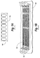
- a memory device 100 may have a number of pins 102 for transferring information from the memory device 100 to a circuit board 104.
- the memory device 100 connects to the circuit board 104 via a slot 106 that extends from the circuit board 104 and is fixed to the circuit board 104.
- the conventional slot 106 is external to the circuit board 104. That is, on the circuit board 104, the slot 106 is provided in a protrusion that attaches to the circuit board 104 and rises from the surface of the circuit board 104.
- the memory device 100 sits inside the slot 106 and is supported on its sides by the external protrusion.
- the conventional memory device 100 is positioned in the slot 106 by pushing the memory module 100 into the slot 106 so that the pins 102 make contact with corresponding interconnects in the slot 106. Once the memory device 100 is seated in the slot 106, the memory device 100 is held in place by friction and may be further secured by actuating one or more clips 108, which lock the memory device 100 into position in the slot 106.
- Fretting is particularly prevalent in the presence of vibration, which is a normal occurrence even on stationary circuit boards. Fretting may become a bigger problem in the presence of a high-vibration environment, such as a circuit board mounted in the head of a missile or on a moving vehicle.
- the conventional slot 106 takes up space on the circuit board 104 beyond the dimensions of the memory device 100. Therefore, the circuit board 104 is larger in length and width (i.e., the x-axis and the y-axis of the board) than might otherwise be necessary in order to accommodate the length and width of the memory device 100. Moreover, because the slot 106 extends upward from the circuit board 104 (i.e., along the z-axis of the board), the circuit board 104, when deployed in conjunction with one or more memory devices 100, is taller than might otherwise be necessary in order to accommodate the height of the memory device 100. This limits the number of circuit boards 104 that can be stacked in a given space, which in turn limits the computing power of a system employing such circuit boards 104.
- Prior art document US5581877 relates to a mounting for a single in-line module including an elongated slot aperture for receiving an edge of the module.
- a circuit board having an internal slot milled to a controlled depth is provided.
- a technology module such as a memory device is provided in the controlled depth slot and secured by an adhesive (e.g., by soldering the memory device into place).
- the controlled depth slot may be provided with a number of semicircular interconnect features, which receive the adhesive and/or guide the adhesive into place.
- the memory device can be secured in a way that reduces vibration issues such as fretting. Accordingly, the circuit board and memory device can be made rugged. Furthermore, because the slot is internal to the circuit board, and because it is not necessary to secure the memory device with clips, the dimensions of the circuit board in each direction (e.g., X-axis, Y-axis, and Z-axis) can be reduced.
- the controlled-depth slot may comprise 1 ⁇ 2 radial plated through-holes to generate one or more solderable 1 ⁇ 2 radial (e.g., in the shape of a "D") interconnect features.
- the slot may include 2 to 3000 1 ⁇ 2 radial interconnect features.
- the slot may include interconnect features on 1 to 5 sides, including the bottom of the slot, and preferably includes interconnect features on 3 to 4 sides.
- Each of the 1 ⁇ 2 radial interconnect features may have a radius, and at least 2 of the 1 ⁇ 2 radial interconnect features may have different radiuses.
- An adhesive such as solder may be provided to the one or more 1 ⁇ 2 radial interconnect features.
- a system including a circuit board having a depth-controlled interconnect slot and one or more solderable technology modules.
- the slot may be internal to the circuit board, and may include one or more 1 ⁇ 2 radial interconnect features on 1 - 5 sides of the slot.
- a solderable technology module may be provided in the slot
- the solderable technology module may be, for example, a memory device, a power device such as Point of Load Supplies (POLS), a security device or anti-tamper device, a capacitance device, or other types of devices such as Field Programmable Gate Arrays (FPGAs).
- a memory module the memory module may include 1 GB to 1000 GB of memory.
- the module may be provided with anti-tamper security features.
- the module may be 0.010 inches to 0.125 inches thick.
- the module may include 2 to 3000 solderable fingers.
- the fingers may include a flat face for receiving solder.
- the fingers may include tin-lead, and may be soldered into the slot using tin-lead solder.
- a method of producing a circuit board and technology module system is provided.
- the method may include generating a slot in the circuit board.
- the slot may be generated by milling the slot into the circuit board to a controlled depth.
- the slot may extend a portion of the depth of the circuit board. For example, the slot may extend at most 1 ⁇ 2 of a depth of the circuit board. If the circuit board includes 24 layers, in some embodiments the slot may extend to at most the 12 th layer.
- the slot may be 0.010 inches to 0.250 inches wide and may extend 0.005 inches to 0.125 inches into the circuit board.
- the method may further include generating one or more 1 ⁇ 2 radial interconnect features on at least one side of the slot.
- the 1 ⁇ 2 radial interconnect features may be provided on 3-4 sides of the slot, and may further be provided on the bottom of the slot.
- the step of generating the one or more 1 ⁇ 2 radial interconnect features may include generating 2 to 3000 radial interconnect features.
- the method may further include providing one or more interconnects on the circuit board connected to the one or more 1 ⁇ 2 radial interconnect features.
- the method may further include inserting a technology module into the slot.
- the technology module may be a memory module.
- the technology module may be secured in a slot of the circuit board.
- the technology module may be secured in the slot by providing an adhesive to the one or more 1 ⁇ 2 radial interconnect features of the slot to secure the module in the slot.
- the adhesive may be solder.
- the slot may be entirely internal to the circuit board such that no portion of the apparatus for connecting the technology module to the circuit board extends above a primary surface of the circuit board.
- a controlled-depth slot extending into a circuit board is provided.
- the controlled depth slot may be milled, and may comprise 1 ⁇ 2 radial plated through-holes to generate a solderable "D" interconnect feature.
- the slot may include interconnect features on one to five sides.
- a circuit board having a depth-controlled interconnect slot is provided in conjunction with one or more solderable technology modules.
- the one or more solderable technology modules may include memory devices, power devices such as Point of Load Supplies (POLS), security devices and anti-tamper devices, capacitance devices, and other types of chips such as Field Programmable Gate Arrays (FPGAs).
- the solderable technology modules may be soldered into the slot to secure the modules in the slot and connect the modules to interconnects on the circuit board.
- a rugged circuit board assembly including one or more secured technology modules may be created.
- the rugged circuit board may exhibit an increased service life due to a reduction in fretting on the technology modules, and further may exhibit reduced dimensions.
- the reduced dimensions may allow the circuit board to be provided in a smaller casing, thereby reducing the overall dimensions of the system in which the circuit board is employed, and/or may allow for more circuit boards to be stacked in the same amount of space.
- a controlled-depth slot is provided in a circuit board.
- a technology module such as the solderable memory module 200 of Figure 2A , may be secured in the controlled-depth slot, such as the controlled-depth slot of Figure 2B .
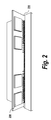
- Figure 2 depicts a solderable memory module 200 suitable for use with the present invention.
- the solderable memory module 200 is secured directly to the board without the use of a separate fastening apparatus such as the external slot 106 and clips 108 of Figure 1B .
- the solderable memory module 200 will be described in detail with respect to Figures 18-24 .
- the solderable memory module 200 is secured to the board using an internal slot 206.
- the slot 206 is described in detail below with respect to Figures 3A through 16 .
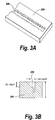
- Figures 3A and 3B depict detailed views of a slot according to exemplary embodiments of the present invention.
- the slot 206 is a recessed portion of the circuit board 204.
- the slot 206 may be entirely internal to the circuit board such that no portion or only a non-substantial portion of the apparatus for connecting the technology module to the circuit board extends above a primary surface of the circuit board.
- the controlled depth slot 206 may be milled into the circuit board using known milling techniques.
- the slot 206 may be 0.010 inches to 0.250 inches wide, and as shown in Figure 3B preferably may be approximately 0.0410 inches wide.
- the width of the slot 206 may depend on the width of the technology module which is to be seated in the slot 206.
- the slot 206 may be 0.005 inches to 0.125 inches deep, and preferably (as shown in Figure 3B ) is 0.0300 +/- 0.0050 inches deep.
- the depth of the slot 206 may depend on a number of factors, such as the height, length, and/or width of the technology module deployed in the slot 206, whether interconnects are provided along the bottom of the slot 206, the depth of the circuit board 204, the configuration of any layers making up the circuit board 204, the strength of the adhesive used to secure the technology module in the slot 206, and other factors.
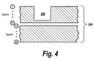
- Figure 4 depicts exemplary depths in a circuit board 204 for a slot 206 according to exemplary embodiments of the present invention.
- the slot 206 may preferably extend into a circuit board 204 a portion of a depth of the circuit board 204, but not entirely through the circuit board 204. In other embodiments, the slot 206 may extend entirely through the circuit board 204.
- the slot 206 may extend up to halfway through the depth of the circuit board 204.
- a circuit board may be formed from a number of discrete layers stacked one on top of the other. If the circuit board 204 includes one or more layers (as shown in Figures 4 and 5 ), the slot 206 may extend through up to half of the layers. In the example depicted in Figure 4 , the circuit board 204 includes 24 layers, and the slot extends through the topmost twelve layers. Because the slot 206 does not pass all the way through the circuit board 204, the bottom twelve layers of the circuit board 204 are advantageously retained for routing information through the bottom twelve layers, allowing the technology module to be seated in the slot 206 while leaving the bottom twelve layers of the circuit board 204 intact for other functions.
- the slot 206 may be sized and dimensioned in order to accommodate a technology module.
- the length of the slot 206 may preferably be .150 to 6.00 inches long.
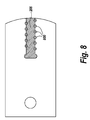
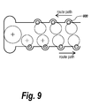
- Figures 8 and 9 provide further exemplary sizes for various components of a slot according to exemplary embodiments of the present invention.
- the slot 206 may include one or more interconnect features 800.
- the interconnect features 800 may be, for example, a 1 ⁇ 2 radial interconnect as described in detail with respect to Figures 10A - 11B .
- Each of the interconnect features 800 may have a radius, such as 0.00295 inches to 0.0061 inches, and at least 2 of the 1 ⁇ 2 radial interconnect features may have different radiuses (allowing, e.g., for the connection of two or more different types of interconnects and/or pins for different purposes such as information transfer and the supplying of power).
- the slot 206 may comprise substantially-1 ⁇ 2-radial plated through-holes to generate one or more solderable "D" interconnect features 800.
- the slot 206 may include 2 to 3000 1 ⁇ 2 radial interconnect features 800.
- the through-holes are described as "1/2 radial" through-holes, it is not necessary that the through-holes be precisely in the shape of 1 ⁇ 2 of a circle.
- a simpler technique for forming the 1 ⁇ 2 radial interconnect features 800 may involve "breaking" a full radial plated thru-hole 100 in half.
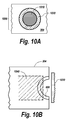
- a plated thru-hole 1000 provided in a circuit board 204 is shown in Figure 10A .
- the plated thru-hole 1000 includes an interior layer 1010 of lead and an exterior layer 1020 of solder.
- an exemplary 1 ⁇ 2 radial interconnect feature 800 suitable for use with exemplary embodiments of the present invention may be formed as one-half of a plated thru-hole 1000.
- the interconnect feature 800 need not be perfectly round, but may also be oval or have multiple rounded protrusions.
- the 1 ⁇ 2 radial interconnect feature 800 of the slot 206 may face a flat surface 1030 of an interconnect provided on the technology module seated in the slot 206.
- Solder 1040 may be provided to the 1 ⁇ 2 radial interconnect feature 800 using a solder mask in order to secure the technology module in the slot 206.
- the technology module is preferably secured in the slot 206 using solder, and more preferably tin-lead solder.
- solder e.g., "fingers” below
- the interconnects (e.g., "fingers" below) of the technology module may also include or be made up of tin-lead. Accordingly, when the tin-lead solder makes contact with the tin-lead interconnects of the technology module, an extremely secure connection can be realized.
- other securing means such as epoxy may be used to secure the technology module in the slot 206.
- the technology module may be secured to one or more internal pads and anti-pads of the circuit board.
- An internal signal pad may have a size, for example, of 0.020 inches, while an internal anti-pad may have a size of 0.028 inches.
- External solder pads may be elongated to provide a robust solder fillet connection between the technology module and circuit board.
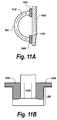
- solder 1040 may attach to the flat surface 1030 of the interconnect without approaching the bottom of the slot 206, as shown in Figure 11B . This may allow for an interconnect to be provided on the bottom of the slot 206 in addition to the sides of the slot 206, as shown in Figure 12A .
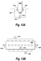
- Figure 12A depicts an exemplary technology module 1200 as shown from the side, and further illustrates locations on the technology module 1200 suitable for placing interconnects.
- first and second interconnect locations 1210, 1220 are provided on respective sides of the technology module 1200.
- a third interconnect location 1230 is provided on the bottom of the technology module 1200.
- the third interconnect location 1230 may connect to an interconnect 1232 provided on the bottom wall of the slot 206.
- Figure 13 depicts a geometry of a solder pad for a slot 206 according to exemplary embodiments of the present invention.
- An internal signal pad may have a size, for example, of 0.020 inches, while an internal anti-pad may have a size of 0.028 inches.
- External solder pads may be elongated to provide a robust solder fillet connection between the technology module and circuit board.
- the 1 ⁇ 2 radial interconnect features 800 may be used to secure a solderable technology module 1200 in the slot 206.
- Figure 14 is an exemplary solder mask for soldering a technology module into a slot
- Figure 15 is an exemplary paste mask for solder paste suitable for securing a technology module into a slot.
- FIG 16 shows an exemplary technology module 1200 secured in the slot.
- the technology module 1200 may be, for example, a memory device, power device such as a Point of Load Supply (POLS), security device or anti-tamper device, capacitance device, or other type of chip such as a Field Programmable Gate Array (FPGA).
- POLS Point of Load Supply
- FPGA Field Programmable Gate Array
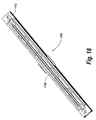
- the solderable technology module 1200 is depicted in more detail in Figures 17 and 18 .
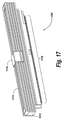
- the solderable technology module 1200 may include a body 1710.
- the body 1710 may support one or more components for providing the functionality of the technology module 1200.
- the components may be memory components.
- the memory module may include 1 GB to 1000 GB of memory split between the memory components.
- the components may also include anti-tamper security features for preventing one or more of the components from being modified by an outside user.
- the body 1710 may be covered by a casing 1712 that is secured in place by a clip 1814.
- the module may be 0.010 inches to 0.125 inches thick.
- Figures 19A-19B depict primary and secondary sides, respectively, of a solderable memory module according to exemplary embodiments of the present invention and component placement on primary and secondary sides, respectively, of a solderable memory module according to exemplary embodiments of the present invention.
- the technology module 1200 may include several components attached to the primary and/or secondary side of the technology module.
- the technology module may be, for example, .150 to 6.00 inches long and .100 to 2.50 inches tall and .001 to .150 deep.
- Figures 20-21 depict a model of such a system which was tested in a simulation in order to predict a likely lifespan of the technology module 1200 in the circuit board 204.
- a wireframe mesh was constructed for the technology module 1200.
- a fine local mesh was constructed for the high stress joints among the fingers of the technology module 1200.
- the random vibration test was performed in accordance with Based on Mil-STD-810F, Method 514.5 for 1 hour per axis on all 3 orthogonal axes at 11.66 GRMs, .1 G 2 /Hz peak.
- the sinusoidal vibration test was based on MIL-HDBK-5400, and was performed for 1 hour per axis on all 3 orthogonal axes with a 75" displacement from 5-15 Hz and 10G peak to peak from 15 to 2000 Hz.
- the mechanical shock test provided 3 shocks per axis in each direction (+/-), with 18 pulses total with a 50Gs, 11msec 1 ⁇ 2 sine pulse normal to the Z axis and 80Gs 11msec 1 ⁇ 2 sine pulses in-plane in the X&Y axis.
- FIG. 23 is a flowchart depicting an exemplary process for producing a circuit board and technology module system according to exemplary embodiments of the present invention, where the technology module is secured in a slot of the circuit board.
- a circuit board may be provided.
- the circuit board may be a printed circuit board having one or more layers.
- one or more interconnects may be provided on the circuit board, for example using surface mount technology.
- a slot may be generated in the circuit board.
- the slot may be generated by milling the slot into the circuit board to a controlled depth.
- the slot may extend a portion of the depth of the circuit board, such as halfway. For example, the slot may extend at most 1 ⁇ 2 of a depth of the circuit board. If the circuit board includes, for example, 24 layers, in some embodiments the slot may extend to at most the 12 th layer.
- the slot may be 0.010 inches to 0.250 inches wide and may extend 0.005 inches to 0.125 inches into the circuit board.
- one or more 1 ⁇ 2 radial interconnect features may be generated on at least one side of the slot.
- the 1 ⁇ 2 radial interconnect features may be provided on 3-4 sides of the slot, and may further be provided on the bottom of the slot.
- the step of generating the one or more 1 ⁇ 2 radial interconnect features may include generating 2 to 3000 radial interconnect features.
- the 1 ⁇ 2 radial interconnect features may be provided by producing full radial interconnect features such as a plated through-hole and "breaking" the full radial interconnect features in half.
- a technology module may be inserted into the slot.
- the technology module may be a memory module.
- the technology module may be secured in a slot of the circuit board.
- the technology module may be secured in the slot by providing an adhesive to the one or more 1 ⁇ 2 radial interconnect features of the slot to secure the module in the slot.
- the adhesive may be solder.
- a rugged circuit board system may be provided.
- the circuit board system may exhibit smaller dimensions than conventional circuit board systems in which an external apparatus is provided for securing a technology module in a slot.
- one or more implementations consistent with principles of the invention may be implemented using one or more devices and/or configurations other than those illustrated in the Figures and described in the Specification.
- One or more devices and/or components may be added and/or removed from the implementations of the figures depending on specific deployments and/or applications.
- one or more disclosed implementations may not be limited to a specific combination of hardware.
Landscapes
- Engineering & Computer Science (AREA)
- Theoretical Computer Science (AREA)
- Computer Hardware Design (AREA)
- Microelectronics & Electronic Packaging (AREA)
- Power Engineering (AREA)
- Human Computer Interaction (AREA)
- Physics & Mathematics (AREA)
- General Engineering & Computer Science (AREA)
- General Physics & Mathematics (AREA)
- Manufacturing & Machinery (AREA)
- Electric Connection Of Electric Components To Printed Circuits (AREA)
- Slot Machines And Peripheral Devices (AREA)
- Combinations Of Printed Boards (AREA)
Description
- The present application claims priority to United States Provisional Application No.
61/530,169, filed September 1, 2011 - The present application pertains to the design and manufacture of circuit boards, and more specifically the connection of devices such as memory modules to circuit boards.
- Conventionally, as shown in
Figures 1A and 1B , amemory device 100 may have a number ofpins 102 for transferring information from thememory device 100 to acircuit board 104. Thememory device 100 connects to thecircuit board 104 via aslot 106 that extends from thecircuit board 104 and is fixed to thecircuit board 104. - The
conventional slot 106 is external to thecircuit board 104. That is, on thecircuit board 104, theslot 106 is provided in a protrusion that attaches to thecircuit board 104 and rises from the surface of thecircuit board 104. Thememory device 100 sits inside theslot 106 and is supported on its sides by the external protrusion. - The
conventional memory device 100 is positioned in theslot 106 by pushing thememory module 100 into theslot 106 so that thepins 102 make contact with corresponding interconnects in theslot 106. Once thememory device 100 is seated in theslot 106, thememory device 100 is held in place by friction and may be further secured by actuating one ormore clips 108, which lock thememory device 100 into position in theslot 106. - This conventional approach suffers from a number of drawbacks. For example, due to the above-described method of securing the
memory device 100 in theslot 106, problems such as fretting are common. Fretting refers to the wear between two surfaces that are in contact with each other under a load. When the two surfaces grind against each other, one or both of the surfaces can wear away. In the case of amemory device 100 connected to acircuit board 104 viapins 102 and interconnects, fretting may cause thepins 102 and interconnects to wear away. Thus, some information that is intended to be transferred between thememory device 100 and thecircuit board 104 may be unable to be transferred due to the absence of a suitable pathway for the information. - Due to the presence of fretting, among other problems, the connection of the
memory device 100 to theboard 104 is not rugged. Both thememory device 100 and theboard 104 are therefore subject to wear and premature failure. - Fretting is particularly prevalent in the presence of vibration, which is a normal occurrence even on stationary circuit boards. Fretting may become a bigger problem in the presence of a high-vibration environment, such as a circuit board mounted in the head of a missile or on a moving vehicle.
- Furthermore, the
conventional slot 106 takes up space on thecircuit board 104 beyond the dimensions of thememory device 100. Therefore, thecircuit board 104 is larger in length and width (i.e., the x-axis and the y-axis of the board) than might otherwise be necessary in order to accommodate the length and width of thememory device 100. Moreover, because theslot 106 extends upward from the circuit board 104 (i.e., along the z-axis of the board), thecircuit board 104, when deployed in conjunction with one ormore memory devices 100, is taller than might otherwise be necessary in order to accommodate the height of thememory device 100. This limits the number ofcircuit boards 104 that can be stacked in a given space, which in turn limits the computing power of a system employingsuch circuit boards 104. - Prior art document
US5581877 relates to a mounting for a single in-line module including an elongated slot aperture for receiving an edge of the module. - A circuit board having an internal slot milled to a controlled depth is provided. A technology module, such as a memory device is provided in the controlled depth slot and secured by an adhesive (e.g., by soldering the memory device into place). In order to facilitate application of the adhesive to the memory device, the controlled depth slot may be provided with a number of semicircular interconnect features, which receive the adhesive and/or guide the adhesive into place.
- Therefore, the memory device can be secured in a way that reduces vibration issues such as fretting. Accordingly, the circuit board and memory device can be made rugged. Furthermore, because the slot is internal to the circuit board, and because it is not necessary to secure the memory device with clips, the dimensions of the circuit board in each direction (e.g., X-axis, Y-axis, and Z-axis) can be reduced.
- For example, according to exemplary embodiments, a controlled-depth slot is provided in a circuit board. The circuit board may be a printed circuit board.
- The controlled depth slot may extend into the circuit board a portion of a depth of the circuit board. The controlled depth slot may be milled into the circuit board. The slot may be, for example, 0.010 inches to 0.250 inches wide, and may be 0.005 inches to 0.125 inches deep.
- The controlled-depth slot may comprise ½ radial plated through-holes to generate one or more solderable ½ radial (e.g., in the shape of a "D") interconnect features. The slot may include 2 to 3000 ½ radial interconnect features. The slot may include interconnect features on 1 to 5 sides, including the bottom of the slot, and preferably includes interconnect features on 3 to 4 sides. Each of the ½ radial interconnect features may have a radius, and at least 2 of the ½ radial interconnect features may have different radiuses. An adhesive such as solder may be provided to the one or more ½ radial interconnect features.
- According to another exemplary embodiment, a system including a circuit board having a depth-controlled interconnect slot and one or more solderable technology modules is provided. The slot may be internal to the circuit board, and may include one or more ½ radial interconnect features on 1 - 5 sides of the slot. A solderable technology module may be provided in the slot
- The solderable technology module may be, for example, a memory device, a power device such as Point of Load Supplies (POLS), a security device or anti-tamper device, a capacitance device, or other types of devices such as Field Programmable Gate Arrays (FPGAs). In the case of a memory module, the memory module may include 1 GB to 1000 GB of memory. The module may be provided with anti-tamper security features. The module may be 0.010 inches to 0.125 inches thick.
- The module may include 2 to 3000 solderable fingers. The fingers may include a flat face for receiving solder. The fingers may include tin-lead, and may be soldered into the slot using tin-lead solder.
- According to another exemplary embodiment, a method of producing a circuit board and technology module system is provided.
- The method may include generating a slot in the circuit board. The slot may be generated by milling the slot into the circuit board to a controlled depth. The slot may extend a portion of the depth of the circuit board. For example, the slot may extend at most ½ of a depth of the circuit board. If the circuit board includes 24 layers, in some embodiments the slot may extend to at most the 12th layer. The slot may be 0.010 inches to 0.250 inches wide and may extend 0.005 inches to 0.125 inches into the circuit board.
- The method may further include generating one or more ½ radial interconnect features on at least one side of the slot. The ½ radial interconnect features may be provided on 3-4 sides of the slot, and may further be provided on the bottom of the slot. The step of generating the one or more ½ radial interconnect features may include generating 2 to 3000 radial interconnect features.
- The method may further include providing one or more interconnects on the circuit board connected to the one or more ½ radial interconnect features.
- The method may further include inserting a technology module into the slot. For example, the technology module may be a memory module.
- The technology module may be secured in a slot of the circuit board. For example, the technology module may be secured in the slot by providing an adhesive to the one or more ½ radial interconnect features of the slot to secure the module in the slot. The adhesive may be solder.
- The slot may be entirely internal to the circuit board such that no portion of the apparatus for connecting the technology module to the circuit board extends above a primary surface of the circuit board.
- Exemplary embodiments of the present invention will be described in detail below with reference to the following figures.
-
Figure 1A depicts a conventional memory module. -
Figure 1B depicts a conventional apparatus for securing the conventional memory module ofFigure 1A to a circuit board. -
Figure 2 depicts a solderable memory module suitable for use with the present invention. -
Figures 3A and 3B depict detailed views of a slot according to exemplary embodiments of the present invention. -
Figure 4 depicts exemplary depths in a circuit board for a slot according to exemplary embodiments of the present invention. -
Figure 5 is a fabrication plan depicting a cross-section of a portion of a printed circuit board suitable for use with exemplary embodiments of the present invention. -
Figures 6A and 6B depict a CAD footprint for a slot according to exemplary embodiments of the present invention. -
Figures 7A and 7B depict exemplary geometries for a slot according to exemplary embodiments of the present invention. -
Figure 8 provides exemplary sizes for various components of a slot according to exemplary embodiments of the present invention. -
Figure 9 is a drill plan depicting exemplary dimensions for a slot and interconnect features according to exemplary embodiments of the present invention. -
Figure 10A depicts a plated-through hole suitable for securing an entity to a printed circuit board using solder. -
Figure 10B depicts a ½ radial interconnect feature suitable for securing a technology module to a circuit board according to exemplary embodiments of the present invention. -
Figures 11A and 11B depict actions of gravity and surface tension which are leveraged to secure a technology module to a circuit board according to exemplary embodiments of the present invention. -
Figures 12A and 12B depict exemplary interconnect locations for a technology module suitable for use with exemplary embodiments of the present invention. -
Figure 13 depicts a geometry of a slot according to exemplary embodiments of the present invention. -
Figure 14 is a solder mask for soldering a technology module into a slot according to exemplary embodiments of the present invention. -
Figure 15 is a paste mask for solder paste suitable for securing a technology module into a slot according to exemplary embodiments of the present invention. -
Figure 16 depicts a solderable technology module soldered into place in a slot according to exemplary embodiments of the present invention. -
Figure 17 depicts an exemplary solderable technology module suitable for use with exemplary embodiments of the present invention. -
Figure 18 is a bottom view of a solderable technology module suitable for use with exemplary embodiments of the present invention. -
Figures 19A and19B depict primary and secondary sides, respectively, of a solderable memory module according to exemplary embodiments of the present invention. -
Figure 20 is a wire mesh view depicting a solderable technology module secured in a slot according to exemplary embodiments of the present invention. -
Figure 21 is a close-up view depicting fingers of a solderable technology module secured in a slot according to exemplary embodiments of the present invention. -
Figure 22 is a graph depicting the results of the stress analysis of the module shown inFigures 20-21 . -
Figure 23 is a flowchart depicting an exemplary process for producing a circuit board and technology module system according to exemplary embodiments of the present invention, where the technology module is secured in a slot of the circuit board. - According to exemplary embodiments, a controlled-depth slot extending into a circuit board is provided. The controlled depth slot may be milled, and may comprise ½ radial plated through-holes to generate a solderable "D" interconnect feature. The slot may include interconnect features on one to five sides. According to another exemplary embodiment, a circuit board having a depth-controlled interconnect slot is provided in conjunction with one or more solderable technology modules. The one or more solderable technology modules may include memory devices, power devices such as Point of Load Supplies (POLS), security devices and anti-tamper devices, capacitance devices, and other types of chips such as Field Programmable Gate Arrays (FPGAs). The solderable technology modules may be soldered into the slot to secure the modules in the slot and connect the modules to interconnects on the circuit board.
- Using the slot, system, and methods described herein, a rugged circuit board assembly including one or more secured technology modules may be created. The rugged circuit board may exhibit an increased service life due to a reduction in fretting on the technology modules, and further may exhibit reduced dimensions. The reduced dimensions may allow the circuit board to be provided in a smaller casing, thereby reducing the overall dimensions of the system in which the circuit board is employed, and/or may allow for more circuit boards to be stacked in the same amount of space.
- According to exemplary embodiments, a controlled-depth slot is provided in a circuit board. A technology module, such as the
solderable memory module 200 ofFigure 2A , may be secured in the controlled-depth slot, such as the controlled-depth slot ofFigure 2B . - In brief summary,
Figure 2 depicts asolderable memory module 200 suitable for use with the present invention. As can be seen inFigure 2 , thesolderable memory module 200 is secured directly to the board without the use of a separate fastening apparatus such as theexternal slot 106 andclips 108 ofFigure 1B . Thesolderable memory module 200 will be described in detail with respect toFigures 18-24 . Thesolderable memory module 200 is secured to the board using aninternal slot 206. Theslot 206 is described in detail below with respect toFigures 3A through 16 . -
Figures 3A and 3B depict detailed views of a slot according to exemplary embodiments of the present invention. As shown inFigure 3A , theslot 206 is a recessed portion of thecircuit board 204. Thus, theslot 206 may be entirely internal to the circuit board such that no portion or only a non-substantial portion of the apparatus for connecting the technology module to the circuit board extends above a primary surface of the circuit board. The controlleddepth slot 206 may be milled into the circuit board using known milling techniques. - The
slot 206 may be 0.010 inches to 0.250 inches wide, and as shown inFigure 3B preferably may be approximately 0.0410 inches wide. The width of theslot 206 may depend on the width of the technology module which is to be seated in theslot 206. - The
slot 206 may be 0.005 inches to 0.125 inches deep, and preferably (as shown inFigure 3B ) is 0.0300 +/- 0.0050 inches deep. The depth of theslot 206 may depend on a number of factors, such as the height, length, and/or width of the technology module deployed in theslot 206, whether interconnects are provided along the bottom of theslot 206, the depth of thecircuit board 204, the configuration of any layers making up thecircuit board 204, the strength of the adhesive used to secure the technology module in theslot 206, and other factors. -
Figure 4 depicts exemplary depths in acircuit board 204 for aslot 206 according to exemplary embodiments of the present invention. As shown inFigure 4 , theslot 206 may preferably extend into a circuit board 204 a portion of a depth of thecircuit board 204, but not entirely through thecircuit board 204. In other embodiments, theslot 206 may extend entirely through thecircuit board 204. - In some embodiments, the
slot 206 may extend up to halfway through the depth of thecircuit board 204. For example, a circuit board may be formed from a number of discrete layers stacked one on top of the other. If thecircuit board 204 includes one or more layers (as shown inFigures 4 and5 ), theslot 206 may extend through up to half of the layers. In the example depicted inFigure 4 , thecircuit board 204 includes 24 layers, and the slot extends through the topmost twelve layers. Because theslot 206 does not pass all the way through thecircuit board 204, the bottom twelve layers of thecircuit board 204 are advantageously retained for routing information through the bottom twelve layers, allowing the technology module to be seated in theslot 206 while leaving the bottom twelve layers of thecircuit board 204 intact for other functions. -
Figure 5 depicts three examples of controlled-depth slots. A first controlled-depth slot 510 extends only through the bottom half of the board (e.g., in a board with 10 layers, the slot extends only through layers 6-10). A second controlled-depth slot 520 may extend all the way through the board (e.g., through layers 1-10). A third controlled-depth slot 530 may extend only through the top half of the board (e.g., only through layers 1-5). - As noted above, the
slot 206 may be sized and dimensioned in order to accommodate a technology module. For example, as shown inFigures 6A and 6B , the length of theslot 206 may preferably be .150 to 6.00 inches long. - Further, as shown in
Figures 7A and 7B , thewalls 710 of theslot 206 need not be provided at 90 degree angles. Preferably, thewalls 710 are provided at an angle extending from thebottom wall 720 of theslot 206 of between 80 degrees and 110 degrees. In some embodiments, as shown inFigure 7B , thewalls 710 may be provided at two or more angles. For example, afirst wall 732 may extend down from the top of theslot 206 at a first angle of 30 degrees to ninety degrees, and thesecond wall 734 may meet thefirst wall 732 at anintermediate point 736 and extend down from theintermediate point 736 to thebottom wall 720 of the slot at a second angle. The second angle may be, for example, 80 degrees to 110 degrees. -
Figures 8 and9 provide further exemplary sizes for various components of a slot according to exemplary embodiments of the present invention. As shown inFigures 8 and9 , theslot 206 may include one or more interconnect features 800. The interconnect features 800 may be, for example, a ½ radial interconnect as described in detail with respect toFigures 10A - 11B . Each of the interconnect features 800 may have a radius, such as 0.00295 inches to 0.0061 inches, and at least 2 of the ½ radial interconnect features may have different radiuses (allowing, e.g., for the connection of two or more different types of interconnects and/or pins for different purposes such as information transfer and the supplying of power). - The
slot 206 may comprise substantially-½-radial plated through-holes to generate one or more solderable "D" interconnect features 800. Theslot 206 may include 2 to 3000 ½ radial interconnect features 800. Although the through-holes are described as "1/2 radial" through-holes, it is not necessary that the through-holes be precisely in the shape of ½ of a circle. - It may be problematic or difficult to manufacture the ½ radial interconnect features directly as a semicircle. Accordingly, a simpler technique for forming the ½ radial interconnect features 800 may involve "breaking" a full radial plated thru-
hole 100 in half. A plated thru-hole 1000 provided in acircuit board 204 is shown inFigure 10A . The plated thru-hole 1000 includes aninterior layer 1010 of lead and anexterior layer 1020 of solder. As shown inFigure 10B , an exemplary ½radial interconnect feature 800 suitable for use with exemplary embodiments of the present invention may be formed as one-half of a plated thru-hole 1000. Theinterconnect feature 800 need not be perfectly round, but may also be oval or have multiple rounded protrusions. - The ½
radial interconnect feature 800 may be provided by forming a full radial interconnect feature such as a plated throughhole 1000, and breaking the full radial interconnect feature in half, for example using a router bit. The router bit may be rotated in a first direction and may approach the full radial interconnect feature from a first side in order to form a break in the full radial interconnect feature on the first side. Then, the direction of the router bit may be reversed, and the router bit may approach the full radial interconnect feature from a second side opposite the first side in order to form a second break in the full radial interconnect feature. Accordingly, half of the full radial interconnect feature may be removed in order to form a ½radial interconnect feature 800. - The ½
radial interconnect feature 800 of theslot 206 may face aflat surface 1030 of an interconnect provided on the technology module seated in theslot 206.Solder 1040 may be provided to the ½radial interconnect feature 800 using a solder mask in order to secure the technology module in theslot 206. - The technology module is preferably secured in the
slot 206 using solder, and more preferably tin-lead solder. If tin-lead solder is used, the interconnects (e.g., "fingers" below) of the technology module may also include or be made up of tin-lead. Accordingly, when the tin-lead solder makes contact with the tin-lead interconnects of the technology module, an extremely secure connection can be realized. Alternatively, other securing means such as epoxy may be used to secure the technology module in theslot 206. - The technology module may be secured to one or more internal pads and anti-pads of the circuit board. An internal signal pad may have a size, for example, of 0.020 inches, while an internal anti-pad may have a size of 0.028 inches. External solder pads may be elongated to provide a robust solder fillet connection between the technology module and circuit board.
- For example, as shown in
Figure 11A , the solder may follow apath 1110 down the ½radial interconnect feature 800 as encouraged by gravity. When the solder approaches and touches theflat surface 1030 of the interconnect,surface tension 1120 may encourage thesolder 1040 to adhere to theflat surface 1030 of the interconnect. - Due to the actions of gravity and surface tension, the
solder 1040 may attach to theflat surface 1030 of the interconnect without approaching the bottom of theslot 206, as shown inFigure 11B . This may allow for an interconnect to be provided on the bottom of theslot 206 in addition to the sides of theslot 206, as shown inFigure 12A . -
Figure 12A depicts anexemplary technology module 1200 as shown from the side, and further illustrates locations on thetechnology module 1200 suitable for placing interconnects. For example, first andsecond interconnect locations technology module 1200. Athird interconnect location 1230 is provided on the bottom of thetechnology module 1200. Thethird interconnect location 1230 may connect to aninterconnect 1232 provided on the bottom wall of theslot 206. - In addition, interconnects may be provided on the front and back of the
technology module 1200. For example, as shown inFigure 12B , afourth interconnect location 1240 may be provided on the front of thetechnology module 1200, and afifth interconnect location 1250 may be provided on the back of thetechnology module 1200. -
Figure 13 depicts a geometry of a solder pad for aslot 206 according to exemplary embodiments of the present invention. An internal signal pad may have a size, for example, of 0.020 inches, while an internal anti-pad may have a size of 0.028 inches. External solder pads may be elongated to provide a robust solder fillet connection between the technology module and circuit board. - The ½ radial interconnect features 800 may be used to secure a
solderable technology module 1200 in theslot 206. For example,Figure 14 is an exemplary solder mask for soldering a technology module into a slot, whileFigure 15 is an exemplary paste mask for solder paste suitable for securing a technology module into a slot. -
Figure 16 shows anexemplary technology module 1200 secured in the slot. Thetechnology module 1200 may be, for example, a memory device, power device such as a Point of Load Supply (POLS), security device or anti-tamper device, capacitance device, or other type of chip such as a Field Programmable Gate Array (FPGA). Thesolderable technology module 1200 is depicted in more detail inFigures 17 and18 . - As shown in
Figures 17 and18 , thesolderable technology module 1200 may include abody 1710. Thebody 1710 may support one or more components for providing the functionality of thetechnology module 1200. For example, if thetechnology module 1200 is a memory module, the components may be memory components. In the case of a memory module, the memory module may include 1 GB to 1000 GB of memory split between the memory components. The components may also include anti-tamper security features for preventing one or more of the components from being modified by an outside user. - The
body 1710 may be covered by acasing 1712 that is secured in place by a clip 1814. In total, the module may be 0.010 inches to 0.125 inches thick. - On the side of the
technology module 1200 that is secured to thecircuit board 204, one ormore interconnects 1720 may be provided. Theinterconnects 1720 may be, for example, fingers extending from the body 1810 of thetechnology module 1200. Each of the fingers may carry information to a corresponding interconnect of thecircuit board 204. Thetechnology module 1200 may include 200 to 300 solderable fingers. The fingers may include a flat face for receiving solder. The fingers may include tin-lead, and may be soldered into the slot using tin-lead solder. -
Figures 19A-19B depict primary and secondary sides, respectively, of a solderable memory module according to exemplary embodiments of the present invention and component placement on primary and secondary sides, respectively, of a solderable memory module according to exemplary embodiments of the present invention. Thetechnology module 1200 may include several components attached to the primary and/or secondary side of the technology module. The technology module may be, for example, .150 to 6.00 inches long and .100 to 2.50 inches tall and .001 to .150 deep. - By securing the above-described
technology module 1200 into theslot 206, a rugged circuit board/technology module system may be realized.Figures 20-21 depict a model of such a system which was tested in a simulation in order to predict a likely lifespan of thetechnology module 1200 in thecircuit board 204. In the model, a wireframe mesh was constructed for thetechnology module 1200. As shown in the close-up inFigure 21 , a fine local mesh was constructed for the high stress joints among the fingers of thetechnology module 1200. - In order to estimate the solder fatigue life of a solder joint as depicted in
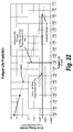
Figures 20-21 , several tests were performed, including a random vibration test, a sinusoidal vibration test, and a mechanical shock test. The results are shown inFigure 22 . - The random vibration test was performed in accordance with Based on Mil-STD-810F, Method 514.5 for 1 hour per axis on all 3 orthogonal axes at 11.66 GRMs, .1 G2/Hz peak. The sinusoidal vibration test was based on MIL-HDBK-5400, and was performed for 1 hour per axis on all 3 orthogonal axes with a 75" displacement from 5-15 Hz and 10G peak to peak from 15 to 2000 Hz. The mechanical shock test provided 3 shocks per axis in each direction (+/-), with 18 pulses total with a 50Gs, 11msec ½ sine pulse normal to the Z axis and 80Gs 11msec ½ sine pulses in-plane in the X&Y axis.
- The quantitative results of the simulation are shown in
Figure 22 . The results were mapped to an extrapolation of Park et al. (2002)'s fatigue life tests for very low stress reversal cycles in a random vibration environment. As a result of the extrapolation, it was concluded that the fatigue life of a solder joint for one of the fingers of thetechnology module 1200 was approximately 1.50 x 10¹⁵ cycles. Because this lifespan dramatically exceeds the useful life of the circuit board/technology module system, the lifespan of the solder joint is deemed to be effectively "infinite." - As a result of these tests, it was determined that, due to the extremely high solder amount per square inch of interconnect, the presently described interconnects and interconnect features provide rugged structural support for the
technology module 1200 in an air cooled module dynamic environment. Thus, this technology significantly reduces technology module fretting reliability issues, particularly those associated with high vibration environments. - In order to achieve such results, the present application also contemplates a method of manufacturing or producing a circuit board having a slot with a technology module secured therein.
Figure 23 is a flowchart depicting an exemplary process for producing a circuit board and technology module system according to exemplary embodiments of the present invention, where the technology module is secured in a slot of the circuit board. - At
step 2310, a circuit board may be provided. The circuit board may be a printed circuit board having one or more layers. Atstep 2320, one or more interconnects may be provided on the circuit board, for example using surface mount technology. - At
step 2330, a slot may be generated in the circuit board. The slot may be generated by milling the slot into the circuit board to a controlled depth. The slot may extend a portion of the depth of the circuit board, such as halfway. For example, the slot may extend at most ½ of a depth of the circuit board. If the circuit board includes, for example, 24 layers, in some embodiments the slot may extend to at most the 12th layer. The slot may be 0.010 inches to 0.250 inches wide and may extend 0.005 inches to 0.125 inches into the circuit board. - At step 2340, one or more ½ radial interconnect features may be generated on at least one side of the slot. The ½ radial interconnect features may be provided on 3-4 sides of the slot, and may further be provided on the bottom of the slot. The step of generating the one or more ½ radial interconnect features may include generating 2 to 3000 radial interconnect features. As noted above, the ½ radial interconnect features may be provided by producing full radial interconnect features such as a plated through-hole and "breaking" the full radial interconnect features in half.
- At
step 2350, a technology module may be inserted into the slot. For example, the technology module may be a memory module. - At
step 2360, the technology module may be secured in a slot of the circuit board. For example, the technology module may be secured in the slot by providing an adhesive to the one or more ½ radial interconnect features of the slot to secure the module in the slot. The adhesive may be solder. - According to the above-described embodiments, a rugged circuit board system may be provided. The circuit board system may exhibit smaller dimensions than conventional circuit board systems in which an external apparatus is provided for securing a technology module in a slot.
- The foregoing description may provide illustration and description of various embodiments of the invention, but is not intended to be exhaustive or to limit the invention to the precise form disclosed. Modifications and variations may be possible in light of the above teachings or may be acquired from practice of the invention. For example, while a series of acts has been described above, the order of the acts may be modified in other implementations consistent with the principles of the invention. Further, non-dependent acts may be performed in parallel. Further, although features and accessing classes have been described above using particular syntaxes, features and accessing classes may equally be specified using in different ways and using different syntaxes.
- In addition, one or more implementations consistent with principles of the invention may be implemented using one or more devices and/or configurations other than those illustrated in the Figures and described in the Specification. One or more devices and/or components may be added and/or removed from the implementations of the figures depending on specific deployments and/or applications. Also, one or more disclosed implementations may not be limited to a specific combination of hardware.
- No element, act, or instruction used in the description of the invention should be construed critical or essential to the invention unless explicitly described as such. Also, as used herein, the article "a" is intended to include one or more items. Where only one item is intended, the term "a single" or similar language is used. Further, the phrase "based on," as used herein is intended to mean "based, at least in part, on" unless explicitly stated otherwise. In addition, the term "user", as used herein, is intended to be broadly interpreted to include, for example, an electronic device (e.g., a workstation) or a user of a electronic device, unless otherwise stated.
- It is intended that the invention not be limited to the particular embodiments disclosed above, but that the invention will include any and all particular embodiments and equivalents falling within the scope of the following appended claims.
Claims (15)
- A circuit board comprising a slot for seating a technology module, the slot comprising:one or more ½ radial interconnect features, the ½ radial interconnect features provided on at least one side of the slot,characterized by the depth of the slot extending a portion of a depth of the circuit board without extending through the entirety of the circuit board, wherein the slot is substantially 0.005 inches to 0.125 inches deep,and wherein each of the radial interconnect features has a radius of 0.00295 inches to 0.0061 inches.
- The circuit board of claim 1, wherein the radial interconnect features are plated through-holes, or
wherein the slot comprises 2 to 3000 ½ radial interconnect features. - The circuit board of claim 1, wherein the ½ radial interconnect features are provided on 3 to 4 sides of the slot, or
wherein each of the ½ radial interconnect features has a radius, and at least two of the ½ radial interconnect features have different radiuses, or
wherein the slot further comprises an interconnect feature provided on the bottom of the slot. - The circuit board of claim 1, wherein the slot is substantially 0.010 inches to 0.250 inches wide.
- The circuit board of claim 1, further comprising an adhesive provided to the one or more ½ radial interconnect features,
wherein the adhesive is preferably solder. - A circuit board assembly, the assembly comprising:a circuit board according to claim 1 anda module provided in the slot.
- The circuit board assembly of claim 6, wherein the module is substantially 0.010 inches to 0.125 inches thick.
- The circuit board assembly of claim 6, wherein the module comprises 200 to 300 solderable fingers,
wherein:the module is preferably secured to the circuit board using solder;the fingers preferably comprise tin-lead; andthe solder preferably comprises tin-lead solder, orwherein the fingers preferably have at least one flat surface for receiving solder. - The circuit board assembly of claim 6, wherein the module is provided with anti-tamper security features, or
wherein the module is a memory module,
wherein the memory module preferably includes 1 GB to 1000 GB of memory. - A method of producing a circuit board comprising a slot, the method comprising:generating one or more ½ radial interconnect features on at least one side of the slot,characterized by generating a slot in the circuit board, the slot extending a portion of a depth of the circuit board without extending through the entirety of the circuit board,wherein the slot extends substantially 0.005 inches to 0.125 inches into the circuit board, and wherein each of the radial interconnect features has a radius of 0.00295 inches to 0.0061 inches.
- The method of claim 10, wherein the ½ radial interconnect features are provided on 3 or 4 sides of the slot, or
wherein the method further comprises providing one or more interconnect features on the bottom of the slot, or
wherein generating the one or more ½ radial interconnect features comprises generating 2 to 3000 radial interconnect features, or
further comprising providing one or more interconnects on the circuit board connected to the one or more ½ radial interconnect features. - The method of claim 10, further comprising:inserting a module into the slot; andproviding an adhesive to the one or more 1/2 radial interconnect features to secure the module in the slot,wherein the adhesive preferably comprises solder.
- The method of claim 10, wherein the module is a memory module, or
wherein the slot is generated by milling the slot into the circuit board, or
wherein the slot is entirely internal to the circuit board. - The method of claim 10, wherein the slot extends at most ½ of a depth of the circuit board,
wherein the circuit board preferably comprises 24 layers, and the slot extends to at most the 12th layer. - The method of claim 10, wherein the slot is substantially 0.010 inches to 0.250 inches wide.
Applications Claiming Priority (2)
| Application Number | Priority Date | Filing Date | Title |
|---|---|---|---|
| US201161530169P | 2011-09-01 | 2011-09-01 | |
| PCT/US2012/053647 WO2013033698A2 (en) | 2011-09-01 | 2012-09-04 | Slot and memory module for a slot standing interconnect |
Publications (2)
| Publication Number | Publication Date |
|---|---|
| EP2751641A2 EP2751641A2 (en) | 2014-07-09 |
| EP2751641B1 true EP2751641B1 (en) | 2016-06-01 |
Family
ID=47018463
Family Applications (1)
| Application Number | Title | Priority Date | Filing Date |
|---|---|---|---|
| EP12772567.9A Active EP2751641B1 (en) | 2011-09-01 | 2012-09-04 | Slot and memory module for a slot standing interconnect |
Country Status (4)
| Country | Link |
|---|---|
| US (1) | US9128679B2 (en) |
| EP (1) | EP2751641B1 (en) |
| CA (1) | CA2847400C (en) |
| WO (1) | WO2013033698A2 (en) |
Families Citing this family (3)
| Publication number | Priority date | Publication date | Assignee | Title |
|---|---|---|---|---|
| US10098241B2 (en) | 2015-10-23 | 2018-10-09 | International Business Machines Corporation | Printed circuit board with edge soldering for high-density packages and assemblies |
| JP6929682B2 (en) * | 2017-03-31 | 2021-09-01 | 住友化学株式会社 | Method for producing lithium nickel composite oxide |
| US10109941B1 (en) * | 2017-06-30 | 2018-10-23 | Intel Corporation | Stepped slot connector to enable low height platforms |
Citations (1)
| Publication number | Priority date | Publication date | Assignee | Title |
|---|---|---|---|---|
| US5581877A (en) * | 1994-09-30 | 1996-12-10 | Allen-Bradley Company, Inc. | Method of fabrication of a circuit board adapted to receive a single in-line module |
Family Cites Families (5)
| Publication number | Priority date | Publication date | Assignee | Title |
|---|---|---|---|---|
| US2825037A (en) | 1955-02-04 | 1958-02-25 | Harry H French | Printed-circuit card clamp |
| US5276817A (en) * | 1990-08-16 | 1994-01-04 | Technosales Company Establishment | System for splitting and connecting computer bus lines |
| TW468927U (en) | 1999-12-23 | 2001-12-11 | Asustek Comp Inc | Computer motherboard and its expanding plate for increasing the expanding slots |
| US6687134B2 (en) | 2002-06-13 | 2004-02-03 | Hewlett-Packard Development Company, L.P. | Card extraction and separation system |
| US8593824B2 (en) * | 2010-10-27 | 2013-11-26 | Verifone, Inc. | Tamper secure circuitry especially for point of sale terminal |
-
2012
- 2012-08-31 US US13/600,810 patent/US9128679B2/en active Active
- 2012-09-04 WO PCT/US2012/053647 patent/WO2013033698A2/en not_active Ceased
- 2012-09-04 CA CA2847400A patent/CA2847400C/en active Active
- 2012-09-04 EP EP12772567.9A patent/EP2751641B1/en active Active
Patent Citations (1)
| Publication number | Priority date | Publication date | Assignee | Title |
|---|---|---|---|---|
| US5581877A (en) * | 1994-09-30 | 1996-12-10 | Allen-Bradley Company, Inc. | Method of fabrication of a circuit board adapted to receive a single in-line module |
Also Published As
| Publication number | Publication date |
|---|---|
| US9128679B2 (en) | 2015-09-08 |
| US20130058050A1 (en) | 2013-03-07 |
| EP2751641A2 (en) | 2014-07-09 |
| WO2013033698A2 (en) | 2013-03-07 |
| WO2013033698A3 (en) | 2013-06-20 |
| CA2847400A1 (en) | 2013-03-07 |
| CA2847400C (en) | 2020-07-14 |
Similar Documents
| Publication | Publication Date | Title |
|---|---|---|
| Singh et al. | Failure modes and mechanisms in electronic packages | |
| KR100344926B1 (en) | Heat sink provided with coupling means, memory module attached with the heat sink and manufacturing method thereof | |
| US20090168363A1 (en) | Thin multi-chip flex module | |
| US9474156B2 (en) | Interposer connectors with alignment features | |
| CN109565934A (en) | Lower groove component placement | |
| JP2012060132A (en) | Electrical component assembly for thermal transfer | |
| AU2005226496A1 (en) | Flexible circuit board assembly | |
| TW201018026A (en) | Modification of connections between a die package and a system board | |
| CA2847400C (en) | Slot and memory module for a slot standing interconnect | |
| US10321580B2 (en) | Integrated circuit package assembly comprising a stack of slanted integrated circuit packages | |
| KR20140127156A (en) | Electrical system and core module thereof | |
| KR20150048105A (en) | Wiring substrate and wiring substrate fabrication method | |
| WO2013040689A1 (en) | Method and apparatus for connecting inlaid chip into printed circuit board | |
| US7005584B2 (en) | Compact navigation device assembly | |
| US11096290B2 (en) | Printed circuit board with edge soldering for high-density packages and assemblies | |
| CN204994085U (en) | A kind of PCB board interconnection structure and PCB board | |
| US20160014879A1 (en) | A printed circuit board (pcb) structure | |
| US20120206892A1 (en) | Circular interposers | |
| WO2006028643A2 (en) | Circuit module system and method | |
| US20090119902A1 (en) | Stacked multiple electronic component interconnect structure | |
| JP7161611B2 (en) | electronic assembly | |
| JP2010118581A (en) | Substrate incorporating electronic components | |
| JP2010129901A (en) | Electronic apparatus, electronic component, and manufacturing method | |
| TWI708336B (en) | 3d electronic module comprising a stack of ball grid array packages | |
| CN214068568U (en) | Capacitor assembly and electronic device |
Legal Events
| Date | Code | Title | Description |
|---|---|---|---|
| PUAI | Public reference made under article 153(3) epc to a published international application that has entered the european phase |
Free format text: ORIGINAL CODE: 0009012 |
|
| 17P | Request for examination filed |
Effective date: 20140327 |
|
| AK | Designated contracting states |
Kind code of ref document: A2 Designated state(s): AL AT BE BG CH CY CZ DE DK EE ES FI FR GB GR HR HU IE IS IT LI LT LU LV MC MK MT NL NO PL PT RO RS SE SI SK SM TR |
|
| DAX | Request for extension of the european patent (deleted) | ||
| 17Q | First examination report despatched |
Effective date: 20150407 |
|
| REG | Reference to a national code |
Ref country code: DE Ref legal event code: R079 Ref document number: 602012019217 Country of ref document: DE Free format text: PREVIOUS MAIN CLASS: G06F0001180000 Ipc: H05K0003360000 |
|
| GRAP | Despatch of communication of intention to grant a patent |
Free format text: ORIGINAL CODE: EPIDOSNIGR1 |
|
| RIC1 | Information provided on ipc code assigned before grant |
Ipc: H01R 12/73 20110101ALI20151123BHEP Ipc: H05K 3/36 20060101AFI20151123BHEP Ipc: G06F 1/18 20060101ALI20151123BHEP |
|
| INTG | Intention to grant announced |
Effective date: 20151218 |
|
| RAP1 | Party data changed (applicant data changed or rights of an application transferred) |
Owner name: MERCURY SYSTEMS INC. |
|
| GRAS | Grant fee paid |
Free format text: ORIGINAL CODE: EPIDOSNIGR3 |
|
| GRAA | (expected) grant |
Free format text: ORIGINAL CODE: 0009210 |
|
| AK | Designated contracting states |
Kind code of ref document: B1 Designated state(s): AL AT BE BG CH CY CZ DE DK EE ES FI FR GB GR HR HU IE IS IT LI LT LU LV MC MK MT NL NO PL PT RO RS SE SI SK SM TR |
|
| REG | Reference to a national code |
Ref country code: GB Ref legal event code: FG4D |
|
| REG | Reference to a national code |
Ref country code: CH Ref legal event code: EP Ref country code: AT Ref legal event code: REF Ref document number: 804530 Country of ref document: AT Kind code of ref document: T Effective date: 20160615 |
|
| REG | Reference to a national code |
Ref country code: IE Ref legal event code: FG4D |
|
| REG | Reference to a national code |
Ref country code: DE Ref legal event code: R096 Ref document number: 602012019217 Country of ref document: DE |
|
| REG | Reference to a national code |
Ref country code: CH Ref legal event code: NV Representative=s name: E. BLUM AND CO. AG PATENT- UND MARKENANWAELTE , CH |
|
| REG | Reference to a national code |
Ref country code: LT Ref legal event code: MG4D |
|
| REG | Reference to a national code |
Ref country code: FR Ref legal event code: PLFP Year of fee payment: 5 |
|
| REG | Reference to a national code |
Ref country code: NL Ref legal event code: MP Effective date: 20160601 |
|
| PG25 | Lapsed in a contracting state [announced via postgrant information from national office to epo] |
Ref country code: LT Free format text: LAPSE BECAUSE OF FAILURE TO SUBMIT A TRANSLATION OF THE DESCRIPTION OR TO PAY THE FEE WITHIN THE PRESCRIBED TIME-LIMIT Effective date: 20160601 Ref country code: FI Free format text: LAPSE BECAUSE OF FAILURE TO SUBMIT A TRANSLATION OF THE DESCRIPTION OR TO PAY THE FEE WITHIN THE PRESCRIBED TIME-LIMIT Effective date: 20160601 Ref country code: NO Free format text: LAPSE BECAUSE OF FAILURE TO SUBMIT A TRANSLATION OF THE DESCRIPTION OR TO PAY THE FEE WITHIN THE PRESCRIBED TIME-LIMIT Effective date: 20160901 |
|
| REG | Reference to a national code |
Ref country code: AT Ref legal event code: MK05 Ref document number: 804530 Country of ref document: AT Kind code of ref document: T Effective date: 20160601 |
|
| PG25 | Lapsed in a contracting state [announced via postgrant information from national office to epo] |
Ref country code: LV Free format text: LAPSE BECAUSE OF FAILURE TO SUBMIT A TRANSLATION OF THE DESCRIPTION OR TO PAY THE FEE WITHIN THE PRESCRIBED TIME-LIMIT Effective date: 20160601 Ref country code: ES Free format text: LAPSE BECAUSE OF FAILURE TO SUBMIT A TRANSLATION OF THE DESCRIPTION OR TO PAY THE FEE WITHIN THE PRESCRIBED TIME-LIMIT Effective date: 20160601 Ref country code: SE Free format text: LAPSE BECAUSE OF FAILURE TO SUBMIT A TRANSLATION OF THE DESCRIPTION OR TO PAY THE FEE WITHIN THE PRESCRIBED TIME-LIMIT Effective date: 20160601 Ref country code: NL Free format text: LAPSE BECAUSE OF FAILURE TO SUBMIT A TRANSLATION OF THE DESCRIPTION OR TO PAY THE FEE WITHIN THE PRESCRIBED TIME-LIMIT Effective date: 20160601 Ref country code: HR Free format text: LAPSE BECAUSE OF FAILURE TO SUBMIT A TRANSLATION OF THE DESCRIPTION OR TO PAY THE FEE WITHIN THE PRESCRIBED TIME-LIMIT Effective date: 20160601 Ref country code: GR Free format text: LAPSE BECAUSE OF FAILURE TO SUBMIT A TRANSLATION OF THE DESCRIPTION OR TO PAY THE FEE WITHIN THE PRESCRIBED TIME-LIMIT Effective date: 20160902 Ref country code: RS Free format text: LAPSE BECAUSE OF FAILURE TO SUBMIT A TRANSLATION OF THE DESCRIPTION OR TO PAY THE FEE WITHIN THE PRESCRIBED TIME-LIMIT Effective date: 20160601 |
|
| PG25 | Lapsed in a contracting state [announced via postgrant information from national office to epo] |
Ref country code: IT Free format text: LAPSE BECAUSE OF FAILURE TO SUBMIT A TRANSLATION OF THE DESCRIPTION OR TO PAY THE FEE WITHIN THE PRESCRIBED TIME-LIMIT Effective date: 20160601 Ref country code: IS Free format text: LAPSE BECAUSE OF FAILURE TO SUBMIT A TRANSLATION OF THE DESCRIPTION OR TO PAY THE FEE WITHIN THE PRESCRIBED TIME-LIMIT Effective date: 20161001 Ref country code: SK Free format text: LAPSE BECAUSE OF FAILURE TO SUBMIT A TRANSLATION OF THE DESCRIPTION OR TO PAY THE FEE WITHIN THE PRESCRIBED TIME-LIMIT Effective date: 20160601 Ref country code: RO Free format text: LAPSE BECAUSE OF FAILURE TO SUBMIT A TRANSLATION OF THE DESCRIPTION OR TO PAY THE FEE WITHIN THE PRESCRIBED TIME-LIMIT Effective date: 20160601 Ref country code: EE Free format text: LAPSE BECAUSE OF FAILURE TO SUBMIT A TRANSLATION OF THE DESCRIPTION OR TO PAY THE FEE WITHIN THE PRESCRIBED TIME-LIMIT Effective date: 20160601 Ref country code: CZ Free format text: LAPSE BECAUSE OF FAILURE TO SUBMIT A TRANSLATION OF THE DESCRIPTION OR TO PAY THE FEE WITHIN THE PRESCRIBED TIME-LIMIT Effective date: 20160601 |
|
| PG25 | Lapsed in a contracting state [announced via postgrant information from national office to epo] |
Ref country code: PT Free format text: LAPSE BECAUSE OF FAILURE TO SUBMIT A TRANSLATION OF THE DESCRIPTION OR TO PAY THE FEE WITHIN THE PRESCRIBED TIME-LIMIT Effective date: 20161003 Ref country code: AT Free format text: LAPSE BECAUSE OF FAILURE TO SUBMIT A TRANSLATION OF THE DESCRIPTION OR TO PAY THE FEE WITHIN THE PRESCRIBED TIME-LIMIT Effective date: 20160601 Ref country code: PL Free format text: LAPSE BECAUSE OF FAILURE TO SUBMIT A TRANSLATION OF THE DESCRIPTION OR TO PAY THE FEE WITHIN THE PRESCRIBED TIME-LIMIT Effective date: 20160601 Ref country code: BE Free format text: LAPSE BECAUSE OF NON-PAYMENT OF DUE FEES Effective date: 20160601 Ref country code: SM Free format text: LAPSE BECAUSE OF FAILURE TO SUBMIT A TRANSLATION OF THE DESCRIPTION OR TO PAY THE FEE WITHIN THE PRESCRIBED TIME-LIMIT Effective date: 20160601 |
|
| REG | Reference to a national code |
Ref country code: DE Ref legal event code: R097 Ref document number: 602012019217 Country of ref document: DE |
|
| PLBE | No opposition filed within time limit |
Free format text: ORIGINAL CODE: 0009261 |
|
| STAA | Information on the status of an ep patent application or granted ep patent |
Free format text: STATUS: NO OPPOSITION FILED WITHIN TIME LIMIT |
|
| PG25 | Lapsed in a contracting state [announced via postgrant information from national office to epo] |
Ref country code: MC Free format text: LAPSE BECAUSE OF FAILURE TO SUBMIT A TRANSLATION OF THE DESCRIPTION OR TO PAY THE FEE WITHIN THE PRESCRIBED TIME-LIMIT Effective date: 20160601 |
|
| 26N | No opposition filed |
Effective date: 20170302 |
|
| PG25 | Lapsed in a contracting state [announced via postgrant information from national office to epo] |
Ref country code: SI Free format text: LAPSE BECAUSE OF FAILURE TO SUBMIT A TRANSLATION OF THE DESCRIPTION OR TO PAY THE FEE WITHIN THE PRESCRIBED TIME-LIMIT Effective date: 20160601 Ref country code: DK Free format text: LAPSE BECAUSE OF FAILURE TO SUBMIT A TRANSLATION OF THE DESCRIPTION OR TO PAY THE FEE WITHIN THE PRESCRIBED TIME-LIMIT Effective date: 20160601 |
|
| REG | Reference to a national code |
Ref country code: IE Ref legal event code: MM4A |
|
| PG25 | Lapsed in a contracting state [announced via postgrant information from national office to epo] |
Ref country code: IE Free format text: LAPSE BECAUSE OF NON-PAYMENT OF DUE FEES Effective date: 20160904 |
|
| PG25 | Lapsed in a contracting state [announced via postgrant information from national office to epo] |
Ref country code: LU Free format text: LAPSE BECAUSE OF NON-PAYMENT OF DUE FEES Effective date: 20160904 |
|
| REG | Reference to a national code |
Ref country code: FR Ref legal event code: PLFP Year of fee payment: 6 |
|
| PG25 | Lapsed in a contracting state [announced via postgrant information from national office to epo] |
Ref country code: CY Free format text: LAPSE BECAUSE OF FAILURE TO SUBMIT A TRANSLATION OF THE DESCRIPTION OR TO PAY THE FEE WITHIN THE PRESCRIBED TIME-LIMIT Effective date: 20160601 Ref country code: HU Free format text: LAPSE BECAUSE OF FAILURE TO SUBMIT A TRANSLATION OF THE DESCRIPTION OR TO PAY THE FEE WITHIN THE PRESCRIBED TIME-LIMIT; INVALID AB INITIO Effective date: 20120904 |
|
| PG25 | Lapsed in a contracting state [announced via postgrant information from national office to epo] |
Ref country code: MT Free format text: LAPSE BECAUSE OF NON-PAYMENT OF DUE FEES Effective date: 20160930 Ref country code: MK Free format text: LAPSE BECAUSE OF FAILURE TO SUBMIT A TRANSLATION OF THE DESCRIPTION OR TO PAY THE FEE WITHIN THE PRESCRIBED TIME-LIMIT Effective date: 20160601 |
|
| PG25 | Lapsed in a contracting state [announced via postgrant information from national office to epo] |
Ref country code: BG Free format text: LAPSE BECAUSE OF FAILURE TO SUBMIT A TRANSLATION OF THE DESCRIPTION OR TO PAY THE FEE WITHIN THE PRESCRIBED TIME-LIMIT Effective date: 20160601 |
|
| REG | Reference to a national code |
Ref country code: FR Ref legal event code: PLFP Year of fee payment: 7 |
|
| PG25 | Lapsed in a contracting state [announced via postgrant information from national office to epo] |
Ref country code: TR Free format text: LAPSE BECAUSE OF FAILURE TO SUBMIT A TRANSLATION OF THE DESCRIPTION OR TO PAY THE FEE WITHIN THE PRESCRIBED TIME-LIMIT Effective date: 20160601 Ref country code: AL Free format text: LAPSE BECAUSE OF FAILURE TO SUBMIT A TRANSLATION OF THE DESCRIPTION OR TO PAY THE FEE WITHIN THE PRESCRIBED TIME-LIMIT Effective date: 20160601 |
|
| P01 | Opt-out of the competence of the unified patent court (upc) registered |
Effective date: 20230508 |
|
| REG | Reference to a national code |
Ref country code: CH Ref legal event code: U11 Free format text: ST27 STATUS EVENT CODE: U-0-0-U10-U11 (AS PROVIDED BY THE NATIONAL OFFICE) Effective date: 20251001 |
|
| PGFP | Annual fee paid to national office [announced via postgrant information from national office to epo] |
Ref country code: DE Payment date: 20250919 Year of fee payment: 14 |
|
| PGFP | Annual fee paid to national office [announced via postgrant information from national office to epo] |
Ref country code: GB Payment date: 20250918 Year of fee payment: 14 |
|
| PGFP | Annual fee paid to national office [announced via postgrant information from national office to epo] |
Ref country code: FR Payment date: 20250922 Year of fee payment: 14 |
|
| PGFP | Annual fee paid to national office [announced via postgrant information from national office to epo] |
Ref country code: CH Payment date: 20251001 Year of fee payment: 14 |