EP2750217A1 - Battery pack - Google Patents
Battery pack Download PDFInfo
- Publication number
- EP2750217A1 EP2750217A1 EP13198830.5A EP13198830A EP2750217A1 EP 2750217 A1 EP2750217 A1 EP 2750217A1 EP 13198830 A EP13198830 A EP 13198830A EP 2750217 A1 EP2750217 A1 EP 2750217A1
- Authority
- EP
- European Patent Office
- Prior art keywords
- battery pack
- bare cell
- recess
- protective circuit
- circuit board
- Prior art date
- Legal status (The legal status is an assumption and is not a legal conclusion. Google has not performed a legal analysis and makes no representation as to the accuracy of the status listed.)
- Withdrawn
Links
Images




Classifications
-
- H—ELECTRICITY
- H01—ELECTRIC ELEMENTS
- H01M—PROCESSES OR MEANS, e.g. BATTERIES, FOR THE DIRECT CONVERSION OF CHEMICAL ENERGY INTO ELECTRICAL ENERGY
- H01M10/00—Secondary cells; Manufacture thereof
- H01M10/05—Accumulators with non-aqueous electrolyte
- H01M10/058—Construction or manufacture
-
- H—ELECTRICITY
- H01—ELECTRIC ELEMENTS
- H01M—PROCESSES OR MEANS, e.g. BATTERIES, FOR THE DIRECT CONVERSION OF CHEMICAL ENERGY INTO ELECTRICAL ENERGY
- H01M50/00—Constructional details or processes of manufacture of the non-active parts of electrochemical cells other than fuel cells, e.g. hybrid cells
- H01M50/50—Current conducting connections for cells or batteries
- H01M50/543—Terminals
-
- H—ELECTRICITY
- H01—ELECTRIC ELEMENTS
- H01M—PROCESSES OR MEANS, e.g. BATTERIES, FOR THE DIRECT CONVERSION OF CHEMICAL ENERGY INTO ELECTRICAL ENERGY
- H01M10/00—Secondary cells; Manufacture thereof
- H01M10/05—Accumulators with non-aqueous electrolyte
- H01M10/052—Li-accumulators
-
- H—ELECTRICITY
- H01—ELECTRIC ELEMENTS
- H01M—PROCESSES OR MEANS, e.g. BATTERIES, FOR THE DIRECT CONVERSION OF CHEMICAL ENERGY INTO ELECTRICAL ENERGY
- H01M10/00—Secondary cells; Manufacture thereof
- H01M10/42—Methods or arrangements for servicing or maintenance of secondary cells or secondary half-cells
- H01M10/425—Structural combination with electronic components, e.g. electronic circuits integrated to the outside of the casing
-
- H—ELECTRICITY
- H01—ELECTRIC ELEMENTS
- H01M—PROCESSES OR MEANS, e.g. BATTERIES, FOR THE DIRECT CONVERSION OF CHEMICAL ENERGY INTO ELECTRICAL ENERGY
- H01M10/00—Secondary cells; Manufacture thereof
- H01M10/42—Methods or arrangements for servicing or maintenance of secondary cells or secondary half-cells
- H01M10/425—Structural combination with electronic components, e.g. electronic circuits integrated to the outside of the casing
- H01M10/4257—Smart batteries, e.g. electronic circuits inside the housing of the cells or batteries
-
- H—ELECTRICITY
- H01—ELECTRIC ELEMENTS
- H01M—PROCESSES OR MEANS, e.g. BATTERIES, FOR THE DIRECT CONVERSION OF CHEMICAL ENERGY INTO ELECTRICAL ENERGY
- H01M50/00—Constructional details or processes of manufacture of the non-active parts of electrochemical cells other than fuel cells, e.g. hybrid cells
- H01M50/10—Primary casings; Jackets or wrappings
- H01M50/147—Lids or covers
-
- H—ELECTRICITY
- H01—ELECTRIC ELEMENTS
- H01M—PROCESSES OR MEANS, e.g. BATTERIES, FOR THE DIRECT CONVERSION OF CHEMICAL ENERGY INTO ELECTRICAL ENERGY
- H01M50/00—Constructional details or processes of manufacture of the non-active parts of electrochemical cells other than fuel cells, e.g. hybrid cells
- H01M50/10—Primary casings; Jackets or wrappings
- H01M50/147—Lids or covers
- H01M50/148—Lids or covers characterised by their shape
- H01M50/15—Lids or covers characterised by their shape for prismatic or rectangular cells
-
- H—ELECTRICITY
- H01—ELECTRIC ELEMENTS
- H01M—PROCESSES OR MEANS, e.g. BATTERIES, FOR THE DIRECT CONVERSION OF CHEMICAL ENERGY INTO ELECTRICAL ENERGY
- H01M50/00—Constructional details or processes of manufacture of the non-active parts of electrochemical cells other than fuel cells, e.g. hybrid cells
- H01M50/50—Current conducting connections for cells or batteries
- H01M50/543—Terminals
- H01M50/547—Terminals characterised by the disposition of the terminals on the cells
- H01M50/55—Terminals characterised by the disposition of the terminals on the cells on the same side of the cell
-
- H—ELECTRICITY
- H01—ELECTRIC ELEMENTS
- H01M—PROCESSES OR MEANS, e.g. BATTERIES, FOR THE DIRECT CONVERSION OF CHEMICAL ENERGY INTO ELECTRICAL ENERGY
- H01M50/00—Constructional details or processes of manufacture of the non-active parts of electrochemical cells other than fuel cells, e.g. hybrid cells
- H01M50/50—Current conducting connections for cells or batteries
- H01M50/543—Terminals
- H01M50/552—Terminals characterised by their shape
- H01M50/553—Terminals adapted for prismatic, pouch or rectangular cells
-
- H—ELECTRICITY
- H01—ELECTRIC ELEMENTS
- H01M—PROCESSES OR MEANS, e.g. BATTERIES, FOR THE DIRECT CONVERSION OF CHEMICAL ENERGY INTO ELECTRICAL ENERGY
- H01M50/00—Constructional details or processes of manufacture of the non-active parts of electrochemical cells other than fuel cells, e.g. hybrid cells
- H01M50/50—Current conducting connections for cells or batteries
- H01M50/572—Means for preventing undesired use or discharge
-
- H—ELECTRICITY
- H01—ELECTRIC ELEMENTS
- H01M—PROCESSES OR MEANS, e.g. BATTERIES, FOR THE DIRECT CONVERSION OF CHEMICAL ENERGY INTO ELECTRICAL ENERGY
- H01M50/00—Constructional details or processes of manufacture of the non-active parts of electrochemical cells other than fuel cells, e.g. hybrid cells
- H01M50/50—Current conducting connections for cells or batteries
- H01M50/572—Means for preventing undesired use or discharge
- H01M50/574—Devices or arrangements for the interruption of current
-
- H—ELECTRICITY
- H01—ELECTRIC ELEMENTS
- H01M—PROCESSES OR MEANS, e.g. BATTERIES, FOR THE DIRECT CONVERSION OF CHEMICAL ENERGY INTO ELECTRICAL ENERGY
- H01M2200/00—Safety devices for primary or secondary batteries
-
- Y—GENERAL TAGGING OF NEW TECHNOLOGICAL DEVELOPMENTS; GENERAL TAGGING OF CROSS-SECTIONAL TECHNOLOGIES SPANNING OVER SEVERAL SECTIONS OF THE IPC; TECHNICAL SUBJECTS COVERED BY FORMER USPC CROSS-REFERENCE ART COLLECTIONS [XRACs] AND DIGESTS
- Y02—TECHNOLOGIES OR APPLICATIONS FOR MITIGATION OR ADAPTATION AGAINST CLIMATE CHANGE
- Y02E—REDUCTION OF GREENHOUSE GAS [GHG] EMISSIONS, RELATED TO ENERGY GENERATION, TRANSMISSION OR DISTRIBUTION
- Y02E60/00—Enabling technologies; Technologies with a potential or indirect contribution to GHG emissions mitigation
- Y02E60/10—Energy storage using batteries
-
- Y—GENERAL TAGGING OF NEW TECHNOLOGICAL DEVELOPMENTS; GENERAL TAGGING OF CROSS-SECTIONAL TECHNOLOGIES SPANNING OVER SEVERAL SECTIONS OF THE IPC; TECHNICAL SUBJECTS COVERED BY FORMER USPC CROSS-REFERENCE ART COLLECTIONS [XRACs] AND DIGESTS
- Y02—TECHNOLOGIES OR APPLICATIONS FOR MITIGATION OR ADAPTATION AGAINST CLIMATE CHANGE
- Y02P—CLIMATE CHANGE MITIGATION TECHNOLOGIES IN THE PRODUCTION OR PROCESSING OF GOODS
- Y02P70/00—Climate change mitigation technologies in the production process for final industrial or consumer products
- Y02P70/50—Manufacturing or production processes characterised by the final manufactured product
Definitions
- the present invention relates to a battery pack.
- the small size and light weight of secondary batteries is also required.
- a material such as lithium having high reactivity is provided to the inside of the secondary battery, the small size and light weight of the secondary battery is limited due to the safety of the secondary battery. Accordingly, a variety of studies have been conducted to develop a secondary battery that can be implemented as a small and light battery pack while improving the safety of the secondary battery.
- Embodiments provide a battery pack having improved safety while being in small in size and light in weight by employing a new structure.
- a battery pack comprising a bare cell, a protective circuit board mounted to the bare cell and a terminal extending through the protective circuit board and having a connection portion where the terminal is connected to the protective circuit board, wherein the bare cell includes a recess at a position corresponding to the connection portion.
- the battery pack may comprise a plurality of terminals each having a corresponding connection portion.
- the recess may extend across all of the connection portions.
- the bare cell may include a plurality of recesses, each recess corresponding to one of the connection portions.
- the battery pack may further comprise an insulating member in the or each recess.
- the bare cell may comprise a cap plate and the or each recess may be formed in the cap plate.
- the depth of the or each recess may be about 20% of the thickness of the cap plate.
- the protection circuit board may be spaced apart from the upper surface of the cap plate.
- the battery pack may further comprise a top case coupled to the bare cell and covering the protective circuit board.
- the or each terminal may be exposed through a corresponding opening formed in the top case.
- the top case may be coupled to the bare cell via coupling members inserted through coupling holes in the ends of the top case, the coupling members engaging with openings in the cap plate.
- the battery pack may further comprise a vent formed in a side wall of the bare cell.
- connection portion may comprise a solder portion.
- connection portion may protrude from the protective circuit board towards the recess.
- an avoidance portion also referred to as a recess
- a connection portion for example, a solder portion formed by soldering a terminal portion to a protective circuit module, so that it is possible to implement the miniaturization of the battery pack while improving the safety of the battery pack by securing a sufficient spacing distance between the solder portion and the bare cell.
- an insulating member is positioned on the avoidance portion, so that it is possible to more effectively prevent an undesired short circuit between the solder portion and the bare cell.
- the battery pack 100 includes a bare cell 110 having a recess 111 formed therein, a protective circuit module 120, a top case 130 covering the protective circuit module 120, and a terminal portion 150 soldered to the protective circuit module 120.
- the recess 111 may be formed at a position corresponding to a solder portion 153 (see FIGS. 3 and 4 ) formed by soldering the terminal portion 150 to the protective circuit module 120.
- the recess may also be referred to as a groove, for example an avoidance groove for avoiding contact between the bare cell and the solder portion.
- the bare cell 110 is a member that generates electrochemical energy through the movement of ions or electrons.
- the bare cell 100 may be manufactured by accommodating an electrode assembly together with an electrolyte in a battery case.
- the electrode assembly is formed by winding a positive electrode plate, a negative plate and a separator interposed therebetween.
- the electrode assembly generates energy by an electrochemical reaction between the electrode assembly and the electrolyte, and the energy is supplied to the outside of the electrode assembly through an electrode tab, etc.
- the battery case may be a pouch-type, prism-type or cylinder-type battery case.
- the recess 111 may be formed in one surface of the bare cell 110.
- the recess 111 may be formed in one surface of the bare cell 110 opposite to the protective circuit module 120.
- the recess 111 may have a shape recessed to have a predetermined depth from the one surface of the bare cell 110.
- the recess 111 may have a substantially uniform depth.
- a vent portion 113 may be further provided as a safety means in the bare cell 110.
- the vent portion 113 serves as a passage along which gas generated inside the bare cell 110 is exhausted to the outside of the bare cell 110.
- the vent portion 113 may be formed on a surface adjacent to the surface in which the recess 111 is formed among the surfaces of the bare cell 110.
- the vent portion 113 may be preferably positioned on a wide surface among the side surfaces of the bare cell 110.
- the protective circuit module 120 is a member positioned on the bare cell 110 so as to control voltage or current in charging and discharging of the bare cell 110.
- the protective circuit module 120 may be implemented as a protective circuit board 123 having a circuit pattern formed thereon, and several electronic components 121 may be mounted on one surface of the protective circuit board 123.
- the electronic components 121 may be a field effect transistor (FET), an integrated circuit IC, etc.
- FET field effect transistor
- the electronic components 121 may perform a function of controlling the electrode assembly in the bare cell 110 or cutting off a circuit in an abnormal operation of the electrode assembly.
- the circuit board 123 of the protective circuit module 120 may include a switching circuit to more efficiently control or protect the battery pack 100 together with the electronic components 121.
- the protective circuit module 120 prevents overcharge, overdischarge, overcurrent, reverse voltage, etc., so that it is possible to prevent explosion, overheating and liquid leakage of the battery pack 100 and the deterioration of charging/discharging characteristics of the battery pack 100. Further, the protective circuit module 120 prevents the degradation of electrical performance and the abnormal operation of the battery pack 100, so that it is possible to eliminate risk factors and to extend the lifespan of the battery pack 100.
- the protective circuit module 120 may be positioned opposite to the surface of the bare cell 110, in which the recess 111 is formed.
- a through-hole 122 may be formed in the protective circuit board 123, and one side 151 of the terminal portion 150 may penetrate the protective circuit board 123 through the through-hole 122.
- the top case 130 is a member coupled to the bare cell 110 so as to cover the protective circuit module 120.
- the top case 130 may be positioned to be coupled to the one surface of the bare cell 110, in which the recess 111 is formed.
- the recess 111, the protective circuit module 120 and the like cannot be exposed to the outside of the battery pack 100 by the top case 130.
- an opening 131 may be formed in the top case 130, and the other side 152 of the terminal portion 150 may be exposed to the outside of the top case 130 through the opening 131.
- a plurality of openings 131 may be implemented according to the number of terminal portions 150. For example, in a case where the terminal portion 150 is configured with three terminal portions, there may be three openings 131.
- the top case 130 may be coupled to the bare cell 110 through a coupling member 140.
- coupling grooves 112 may be formed at both sides of the bare cell 110, respectively, and coupling grooves 132 may be formed at both sides of the top case 130, respectively.
- the coupling grooves 112 and 132 are formed at positions corresponding to each other.
- the coupling member 140 is inserted into the coupling grooves 112 and 132, so that the bare cell 110 and the top case 130 can be coupled to each other.
- a screw thread may be formed inside the coupling grooves 112 and 132, and the coupling member 140 may be implemented as a bolt to be screw-coupled in the coupling grooves 112 and 132.
- a bonding member 141 covering a head portion of the coupling member 140 so that the coupling member 140 is not exposed to the outside may further be positioned at an upper portion of the coupling member 140.
- the terminal portion 150 is a member that allows the battery pack 100 and an external device to be electrically connected.
- the terminal portion 150 may be positioned on one surface, for example a top surface, of the protective circuit board 123, and the one side 151 of the terminal portion 150 may be soldered to the other surface, for example the bottom surface, of the protective circuit board 123 by passing through the through-hole 122 of the protective circuit board 123.
- the top surface of the protective circuit board 123 is the surface that faces the top cap and the bottom surface is the surface that faces the bare cell.
- the one side 151 of the terminal portion 150 may be extended toward the recess 111 by passing through the through-hole 122 of the protective circuit board 123.
- the one side 151 of the terminal portion 150 may be positioned to be spaced apart from the recess 111.
- the one side 151 of the terminal portion 150 may be soldered to the bottom surface of the protective circuit board 123 so as to be electrically connected to the circuit pattern formed on that surface of the protective circuit board 123.
- terminal portions 150 There may be a plurality of terminal portions 150, e.g., three.
- the one side 151 of the terminal portion 150 may be connected to the protective circuit board 123 through soldering, and the other side 152 of the terminal portion 150 may be exposed to the outside through the opening 131 formed in the top case 130.
- the external device is connected to terminal portion 150 exposed through the opening 131, so that the battery pack 100 and the external device can be electrically connected to each other.
- the shape of the terminal portion shown in these figures is merely an example, and the present invention is not limited thereto. That is, the terminal portion 150 may be implemented in various shapes known in the art.
- the battery pack 100 may further include a protective element 160, a bottom case 170, a label 180, etc.
- the protective element 160 is a member interposed between the protective circuit module 120 and the bare cell 110 so as to cut off current by increasing resistance when temperature increases.
- the protective element 160 may use, for example, a positive temperature coefficient (PTC) element.
- PTC positive temperature coefficient
- the protective element 160 may be connected to the bare cell 110 through a protective element tape 161.
- the bottom case 170 is a member coupled to a surface opposite to the surface of the bare cell 110, to which the top case 130 is coupled.
- the bottom case 170 is used to protect the bare cell 110.
- the bottom case 170 may be coupled to the bare cell 110, for example, through an adhesive member 171.
- the label 180 is a member that surrounds the side surface of the bare cell 110 to which the top case 130 and the bottom case 170 are coupled, so that it is possible to enhance the coupling among the top case 130, the bottom case 170 and the bare cell 110 and to protect the bare cell 110 from the outside.
- information on the battery pack 110, the manufacturer and the like may be recorded on the label 180.
- FIG. 3 is a sectional view of the battery pack 100 taken along line A1-A1' of FIG. 1 .
- FIG. 4 is a sectional view of the battery pack 100 taken along line B1-B1' of FIG. 1 .
- the relationship between the recess 111 and the solder portion 153 in the battery pack 100 according to this embodiment will be described in detail with reference to FIGS. 3 and 4 .
- the one side 151 of the terminal portion 150 may be soldered to the bottom surface of the protective circuit board 123 by passing through the through-hole 122 of the protective circuit board 123. As a result, the solder portion 153 protrudes from the bottom surface of the protective circuit board 123.
- the solder portion 153 Since the solder portion 153 is implemented to protrude from the bottom surface of the protective circuit board 123, the solder portion 153 may come in direct contact with the bare cell 110 due to an external impact, etc. Therefore, it is important that a sufficient separate space should be formed between the solder portion 153 and the bare cell 110. Generally, the height of the separate space between the solder portion 153 and the bare cell 110 may be about 1.1mm. However, as the separate space between the solder portion 153 and the bare cell 110 increases, the size of the battery pack 100 may increase. If the size of the battery pack 100 does not increase, the size of the bare cell 110 is relatively decreased, and therefore, the capacity of the battery pack 100 may be reduced. Accordingly, it is required to propose a plan for ensuring a sufficient space between the solder portion 153 and the bare cell 110 while maintaining the entire size of the battery pack 100 and the capacity of the bare cell 110.
- the recess 111 is formed in the bare cell 110, thereby solving the problem described above. Specifically, if the recess 111 is formed at the position corresponding to the solder portion 153, in this case under the solder portion 153, a relatively large interval between the solder portion 153 and the bare cell 110 can be ensured, so that it is possible to decrease the possibility that the solder portion 153 and the bare cell 110 will come in contact with each other. Since the spacing between the solder portion 153 and the bare cell 110 other than at the recess 111 can be narrowed, there is no concern that the entire size of the battery pack 100 increases, and the capacity of the bare cell 110 can be maintained.
- the depth of the recess 111 may be 20% of the thickness of the cap plate 115.
- the depth of the recess 111 may be 0.2mm.
- the gap between the circuit board 123 and the bare cell can be minimised while avoiding the risk of the solder portion 153 touching the bare cell, since a suitable gap can be provided between the bottom of the solder portion and the bottom of the recess.
- a plurality of terminal portions 150 may be provided and a plurality of solder portions 153 may also be provided. Therefore, the solder portion may be positioned at the one side 151 of each terminal portion 150.
- the recess 111 may be implemented to have a size corresponding to the whole of the plurality of solder portions 153.
- the recess 111 may be implemented to have a size capable of corresponding to the whole of the three solder portions 153.
- any solder portion 153 can be sufficiently spaced apart from the bare cell 110 by the recess 111.
- FIG. 5 is a sectional view showing a case where an insulating member 114 is further positioned on the recess 111 of the battery pack 100 shown in FIG. 3 .
- the insulating member 114 may be further positioned on the recess 111, and accordingly, it is possible to more effectively prevent a short circuit between the terminal portion 150 and the bare cell 110.
- the insulating member 114 may be implemented by, for example, a single-faced or double-face tape, and the insulating member 114 may be arranged to fit into the recess 111.
- FIG. 6 is a perspective view of a battery pack 200 according to another embodiment of the present invention.
- FIG. 7 is an exploded perspective view of the battery pack 200 shown in FIG. 6 .
- FIG. 8 is a sectional view of the battery pack 200 taken along line A2-A2' of FIG. 6 .
- FIG. 9 is a sectional view of the battery pack 200 taken along line B2-B2' of FIG. 6 .
- the battery pack 200 includes a bare cell 210 having a recess 211 formed therein, a protective circuit module 220, a top case 230 covering the protective circuit module 220, and a terminal portion 250 soldered to the protective circuit module 220.
- a plurality of recesses 211 may be formed, and the plurality of recesses may be respectively formed at positions corresponding to solder portions 253 (see FIGS. 8 and 9 ) formed by soldering the terminal portion 250 to the protective circuit board 223 of the protective circuit module 220.
- the recesses are formed under the solder portions in the view shown in Figures 8 and 9 .
- the recess 211 of the battery pack 200 is not implemented as one large recess, like the recess 111 shown in FIG. 2 , but implemented as a plurality of recesses so that the plurality of recesses correspond to the plurality of solder portions 253, respectively.
- the recess 211 may also be configured with three recesses so that the recesses correspond to the respective solder portions 253.
- the alignment reference can be set when the top case 230 is mounted to the bare cell 210, in addition to the prevention of a short circuit between the solder portion 253 and the bare cell 210, the prevention of an increase in the size of the battery pack 100, and the prevention of a decrease in the capacity of the bare cell 210.
- the top case 230 can be aligned on the bare cell 210 so that the recesses 211 are positioned below the respective solder portions 253 when the top case 230 is mounted to the bare cell 210.
- a coupling member 240 is inserted into coupling grooves 212 and 232, so that the top case 230 and the bare cell 210 can be easily coupled to each other.
- insulating members (not shown) corresponding to insulating member 114 may be inserted into the or each recess.
- solder portion 153, 253 is specifically described, the principles of the invention also apply to other types of connection between the terminals and the protective circuit board (123, 223), for example a welded or mechanically connected portion.
Landscapes
- Chemical & Material Sciences (AREA)
- Chemical Kinetics & Catalysis (AREA)
- Electrochemistry (AREA)
- General Chemical & Material Sciences (AREA)
- Engineering & Computer Science (AREA)
- Manufacturing & Machinery (AREA)
- Microelectronics & Electronic Packaging (AREA)
- Battery Mounting, Suspending (AREA)
- Connection Of Batteries Or Terminals (AREA)
Abstract
Description
- The present invention relates to a battery pack.
- Recently, secondary batteries have been variously used as power sources of portable electronic devices. As the portable electronic devices are used in various fields, demands on secondary batteries are rapidly increased. The secondary batteries can be charged/discharged a plurality of times, and accordingly are economically and environmentally efficient. Thus, the use of the battery packs is encouraged.
- As the small size and light weight of electronic devices is required, the small size and light weight of secondary batteries is also required. However, since a material such as lithium having high reactivity is provided to the inside of the secondary battery, the small size and light weight of the secondary battery is limited due to the safety of the secondary battery. Accordingly, a variety of studies have been conducted to develop a secondary battery that can be implemented as a small and light battery pack while improving the safety of the secondary battery.
- Embodiments provide a battery pack having improved safety while being in small in size and light in weight by employing a new structure.
- According to an aspect of the present invention, there is provided a battery pack comprising a bare cell, a protective circuit board mounted to the bare cell and a terminal extending through the protective circuit board and having a connection portion where the terminal is connected to the protective circuit board, wherein the bare cell includes a recess at a position corresponding to the connection portion.
- The battery pack may comprise a plurality of terminals each having a corresponding connection portion.
- The recess may extend across all of the connection portions.
- The bare cell may include a plurality of recesses, each recess corresponding to one of the connection portions.
- The battery pack may further comprise an insulating member in the or each recess.
- The bare cell may comprise a cap plate and the or each recess may be formed in the cap plate. The depth of the or each recess may be about 20% of the thickness of the cap plate.
- The protection circuit board may be spaced apart from the upper surface of the cap plate.
- The battery pack may further comprise a top case coupled to the bare cell and covering the protective circuit board. The or each terminal may be exposed through a corresponding opening formed in the top case.
- The top case may be coupled to the bare cell via coupling members inserted through coupling holes in the ends of the top case, the coupling members engaging with openings in the cap plate.
- The battery pack may further comprise a vent formed in a side wall of the bare cell.
- The connection portion may comprise a solder portion.
- The connection portion may protrude from the protective circuit board towards the recess.
- Other features and advantages of the present invention will become more fully apparent from the following detailed description, taken in conjunction with the accompanying drawings.
- According to the battery pack of the present invention, an avoidance portion, also referred to as a recess, is formed in a bare cell so as to correspond to a connection portion, for example, a solder portion formed by soldering a terminal portion to a protective circuit module, so that it is possible to implement the miniaturization of the battery pack while improving the safety of the battery pack by securing a sufficient spacing distance between the solder portion and the bare cell.
- Further, an insulating member is positioned on the avoidance portion, so that it is possible to more effectively prevent an undesired short circuit between the solder portion and the bare cell.
- The accompanying drawings, together with the specification, illustrate exemplary embodiments of the present invention, and, together with the description, serve to explain the principles of the present invention.
-
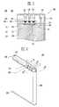
FIG. 1 is a perspective view of a battery pack according to an embodiment of the present invention; -
FIG. 2 is an exploded perspective view of the battery pack shown inFIG. 1 ; -
FIG. 3 is a sectional view of the battery pack taken along line A1-A1' ofFIG. 1 ; -
FIG. 4 is a sectional view of the battery pack taken along line B1-B1' ofFIG. 1 ; -
FIG. 5 is a sectional view showing a case where an insulating member is further positioned on a recess of the battery pack shown inFIG. 3 ; -
FIG. 6 is a perspective view of a battery pack according to another embodiment of the present invention; -
FIG. 7 is an exploded perspective view of the battery pack shown inFIG. 6 ; -
FIG. 8 is a sectional view of the battery pack taken along line A2-A2' ofFIG. 6 ; and -
FIG. 9 is a sectional view of the battery pack taken along line B2-B2' ofFIG. 6 . - Hereinafter, the
battery pack 100 according to one embodiment will be described with reference toFIGS. 1 and2 . - As shown in
FIGS. 1 and2 , thebattery pack 100 according to this embodiment includes abare cell 110 having arecess 111 formed therein, aprotective circuit module 120, atop case 130 covering theprotective circuit module 120, and aterminal portion 150 soldered to theprotective circuit module 120. Therecess 111 may be formed at a position corresponding to a solder portion 153 (seeFIGS. 3 and 4 ) formed by soldering theterminal portion 150 to theprotective circuit module 120. The recess may also be referred to as a groove, for example an avoidance groove for avoiding contact between the bare cell and the solder portion. - The
bare cell 110 is a member that generates electrochemical energy through the movement of ions or electrons. - The
bare cell 100 may be manufactured by accommodating an electrode assembly together with an electrolyte in a battery case. Here, the electrode assembly is formed by winding a positive electrode plate, a negative plate and a separator interposed therebetween. The electrode assembly generates energy by an electrochemical reaction between the electrode assembly and the electrolyte, and the energy is supplied to the outside of the electrode assembly through an electrode tab, etc. For example, the battery case may be a pouch-type, prism-type or cylinder-type battery case. - The
recess 111 may be formed in one surface of thebare cell 110. Here, therecess 111 may be formed in one surface of thebare cell 110 opposite to theprotective circuit module 120. Therecess 111 may have a shape recessed to have a predetermined depth from the one surface of thebare cell 110. Therecess 111 may have a substantially uniform depth. - Meanwhile, a
vent portion 113 may be further provided as a safety means in thebare cell 110. Here, thevent portion 113 serves as a passage along which gas generated inside thebare cell 110 is exhausted to the outside of thebare cell 110. Thevent portion 113 may be formed on a surface adjacent to the surface in which therecess 111 is formed among the surfaces of thebare cell 110. When considering that thevent portion 113 is formed in a linear shape as shown inFIG. 2 , thevent portion 113 may be preferably positioned on a wide surface among the side surfaces of thebare cell 110. - The
protective circuit module 120 is a member positioned on thebare cell 110 so as to control voltage or current in charging and discharging of thebare cell 110. - The
protective circuit module 120 may be implemented as aprotective circuit board 123 having a circuit pattern formed thereon, and severalelectronic components 121 may be mounted on one surface of theprotective circuit board 123. Here, theelectronic components 121 may be a field effect transistor (FET), an integrated circuit IC, etc. Theelectronic components 121 may perform a function of controlling the electrode assembly in thebare cell 110 or cutting off a circuit in an abnormal operation of the electrode assembly. Thecircuit board 123 of theprotective circuit module 120 may include a switching circuit to more efficiently control or protect thebattery pack 100 together with theelectronic components 121. Specifically, theprotective circuit module 120 prevents overcharge, overdischarge, overcurrent, reverse voltage, etc., so that it is possible to prevent explosion, overheating and liquid leakage of thebattery pack 100 and the deterioration of charging/discharging characteristics of thebattery pack 100. Further, theprotective circuit module 120 prevents the degradation of electrical performance and the abnormal operation of thebattery pack 100, so that it is possible to eliminate risk factors and to extend the lifespan of thebattery pack 100. - The
protective circuit module 120 may be positioned opposite to the surface of thebare cell 110, in which therecess 111 is formed. A through-hole 122 may be formed in theprotective circuit board 123, and oneside 151 of theterminal portion 150 may penetrate theprotective circuit board 123 through the through-hole 122. - The
top case 130 is a member coupled to thebare cell 110 so as to cover theprotective circuit module 120. - The
top case 130 may be positioned to be coupled to the one surface of thebare cell 110, in which therecess 111 is formed. Thus, therecess 111, theprotective circuit module 120 and the like cannot be exposed to the outside of thebattery pack 100 by thetop case 130. Meanwhile, anopening 131 may be formed in thetop case 130, and theother side 152 of theterminal portion 150 may be exposed to the outside of thetop case 130 through theopening 131. In this case, a plurality ofopenings 131 may be implemented according to the number ofterminal portions 150. For example, in a case where theterminal portion 150 is configured with three terminal portions, there may be threeopenings 131. - The
top case 130 may be coupled to thebare cell 110 through acoupling member 140. In this case,coupling grooves 112 may be formed at both sides of thebare cell 110, respectively, andcoupling grooves 132 may be formed at both sides of thetop case 130, respectively. Thecoupling grooves coupling member 140 is inserted into thecoupling grooves bare cell 110 and thetop case 130 can be coupled to each other. For example, a screw thread may be formed inside thecoupling grooves coupling member 140 may be implemented as a bolt to be screw-coupled in thecoupling grooves bonding member 141 covering a head portion of thecoupling member 140 so that thecoupling member 140 is not exposed to the outside may further be positioned at an upper portion of thecoupling member 140. - The
terminal portion 150 is a member that allows thebattery pack 100 and an external device to be electrically connected. - The
terminal portion 150 may be positioned on one surface, for example a top surface, of theprotective circuit board 123, and the oneside 151 of theterminal portion 150 may be soldered to the other surface, for example the bottom surface, of theprotective circuit board 123 by passing through the through-hole 122 of theprotective circuit board 123. Although the battery may be oriented in various ways, the top surface of theprotective circuit board 123 is the surface that faces the top cap and the bottom surface is the surface that faces the bare cell. In this case, the oneside 151 of theterminal portion 150 may be extended toward therecess 111 by passing through the through-hole 122 of theprotective circuit board 123. The oneside 151 of theterminal portion 150 may be positioned to be spaced apart from therecess 111. The oneside 151 of theterminal portion 150 may be soldered to the bottom surface of theprotective circuit board 123 so as to be electrically connected to the circuit pattern formed on that surface of theprotective circuit board 123. - There may be a plurality of
terminal portions 150, e.g., three. The oneside 151 of theterminal portion 150 may be connected to theprotective circuit board 123 through soldering, and theother side 152 of theterminal portion 150 may be exposed to the outside through theopening 131 formed in thetop case 130. Thus, the external device is connected toterminal portion 150 exposed through theopening 131, so that thebattery pack 100 and the external device can be electrically connected to each other. - Meanwhile, the shape of the terminal portion shown in these figures is merely an example, and the present invention is not limited thereto. That is, the
terminal portion 150 may be implemented in various shapes known in the art. - The
battery pack 100 may further include aprotective element 160, abottom case 170, alabel 180, etc. - The
protective element 160 is a member interposed between theprotective circuit module 120 and thebare cell 110 so as to cut off current by increasing resistance when temperature increases. In order to perform such a function, theprotective element 160 may use, for example, a positive temperature coefficient (PTC) element. Theprotective element 160 may be connected to thebare cell 110 through aprotective element tape 161. - The
bottom case 170 is a member coupled to a surface opposite to the surface of thebare cell 110, to which thetop case 130 is coupled. Thebottom case 170 is used to protect thebare cell 110. In this embodiment, thebottom case 170 may be coupled to thebare cell 110, for example, through anadhesive member 171. - The
label 180 is a member that surrounds the side surface of thebare cell 110 to which thetop case 130 and thebottom case 170 are coupled, so that it is possible to enhance the coupling among thetop case 130, thebottom case 170 and thebare cell 110 and to protect thebare cell 110 from the outside. In this case, information on thebattery pack 110, the manufacturer and the like may be recorded on thelabel 180. -
FIG. 3 is a sectional view of thebattery pack 100 taken along line A1-A1' ofFIG. 1 .FIG. 4 is a sectional view of thebattery pack 100 taken along line B1-B1' ofFIG. 1 . Hereinafter, the relationship between therecess 111 and thesolder portion 153 in thebattery pack 100 according to this embodiment will be described in detail with reference toFIGS. 3 and 4 . - As shown in
FIGS. 3 and 4 , the oneside 151 of theterminal portion 150 may be soldered to the bottom surface of theprotective circuit board 123 by passing through the through-hole 122 of theprotective circuit board 123. As a result, thesolder portion 153 protrudes from the bottom surface of theprotective circuit board 123. - Since the
solder portion 153 is implemented to protrude from the bottom surface of theprotective circuit board 123, thesolder portion 153 may come in direct contact with thebare cell 110 due to an external impact, etc. Therefore, it is important that a sufficient separate space should be formed between thesolder portion 153 and thebare cell 110. Generally, the height of the separate space between thesolder portion 153 and thebare cell 110 may be about 1.1mm. However, as the separate space between thesolder portion 153 and thebare cell 110 increases, the size of thebattery pack 100 may increase. If the size of thebattery pack 100 does not increase, the size of thebare cell 110 is relatively decreased, and therefore, the capacity of thebattery pack 100 may be reduced. Accordingly, it is required to propose a plan for ensuring a sufficient space between thesolder portion 153 and thebare cell 110 while maintaining the entire size of thebattery pack 100 and the capacity of thebare cell 110. - In this embodiment, the
recess 111 is formed in thebare cell 110, thereby solving the problem described above. Specifically, if therecess 111 is formed at the position corresponding to thesolder portion 153, in this case under thesolder portion 153, a relatively large interval between thesolder portion 153 and thebare cell 110 can be ensured, so that it is possible to decrease the possibility that thesolder portion 153 and thebare cell 110 will come in contact with each other. Since the spacing between thesolder portion 153 and thebare cell 110 other than at therecess 111 can be narrowed, there is no concern that the entire size of thebattery pack 100 increases, and the capacity of thebare cell 110 can be maintained. In this case, the depth of therecess 111 may be 20% of the thickness of thecap plate 115. For example, when the thickness of thecap plate 115 is 1mm, the depth of therecess 111 may be 0.2mm. In other words, the gap between thecircuit board 123 and the bare cell can be minimised while avoiding the risk of thesolder portion 153 touching the bare cell, since a suitable gap can be provided between the bottom of the solder portion and the bottom of the recess. - Meanwhile, in this embodiment, a plurality of
terminal portions 150 may be provided and a plurality ofsolder portions 153 may also be provided. Therefore, the solder portion may be positioned at the oneside 151 of eachterminal portion 150. Therecess 111 may be implemented to have a size corresponding to the whole of the plurality ofsolder portions 153. For example, in a case where thesolder portion 150 is configured with three solder portions, therecess 111 may be implemented to have a size capable of corresponding to the whole of the threesolder portions 153. Thus, anysolder portion 153 can be sufficiently spaced apart from thebare cell 110 by therecess 111. -
FIG. 5 is a sectional view showing a case where an insulatingmember 114 is further positioned on therecess 111 of thebattery pack 100 shown inFIG. 3 . - Referring to
FIG. 5 , the insulatingmember 114 may be further positioned on therecess 111, and accordingly, it is possible to more effectively prevent a short circuit between theterminal portion 150 and thebare cell 110. In this case, the insulatingmember 114 may be implemented by, for example, a single-faced or double-face tape, and the insulatingmember 114 may be arranged to fit into therecess 111. -
FIG. 6 is a perspective view of abattery pack 200 according to another embodiment of the present invention.FIG. 7 is an exploded perspective view of thebattery pack 200 shown inFIG. 6 .FIG. 8 is a sectional view of thebattery pack 200 taken along line A2-A2' ofFIG. 6 .FIG. 9 is a sectional view of thebattery pack 200 taken along line B2-B2' ofFIG. 6 . - Hereinafter, the
battery pack 200 according to this embodiment will be described in detail with reference toFIGS. 6 to 9 . Thebattery pack 200 according to this embodiment includes abare cell 210 having arecess 211 formed therein, aprotective circuit module 220, atop case 230 covering theprotective circuit module 220, and aterminal portion 250 soldered to theprotective circuit module 220. A plurality ofrecesses 211 may be formed, and the plurality of recesses may be respectively formed at positions corresponding to solder portions 253 (seeFIGS. 8 and 9 ) formed by soldering theterminal portion 250 to theprotective circuit board 223 of theprotective circuit module 220. For example, the recesses are formed under the solder portions in the view shown inFigures 8 and 9 . - That is, the
recess 211 of thebattery pack 200 according to this embodiment is not implemented as one large recess, like therecess 111 shown inFIG. 2 , but implemented as a plurality of recesses so that the plurality of recesses correspond to the plurality ofsolder portions 253, respectively. For example, in a case where thesolder portion 253 is configured with three solder portions, therecess 211 may also be configured with three recesses so that the recesses correspond to therespective solder portions 253. In this embodiment, in a case where therecesses 211 are implemented to correspond to therespective solder portions 253, the alignment reference can be set when thetop case 230 is mounted to thebare cell 210, in addition to the prevention of a short circuit between thesolder portion 253 and thebare cell 210, the prevention of an increase in the size of thebattery pack 100, and the prevention of a decrease in the capacity of thebare cell 210. Specifically, since the recesses are implemented to correspond to therespective solder portions 253, thetop case 230 can be aligned on thebare cell 210 so that therecesses 211 are positioned below therespective solder portions 253 when thetop case 230 is mounted to thebare cell 210. Subsequently, acoupling member 240 is inserted intocoupling grooves top case 230 and thebare cell 210 can be easily coupled to each other. - As in the first embodiment, insulating members (not shown) corresponding to insulating
member 114 may be inserted into the or each recess. - Although in the above description a
solder portion - While the present invention has been described in connection with certain exemplary embodiments, it is to be understood that the invention is not limited to the disclosed embodiments, but, on the contrary, is intended to cover various modifications and equivalent arrangements included within the scope of the appended claims.
Claims (14)
- A battery pack (100, 200), comprising:a bare cell (110, 210);a protective circuit board (123, 223) mounted to the bare cell; anda terminal (150, 250) extending through the protective circuit board and having a connection portion (153, 253) where the terminal is connected to the protective circuit board,wherein the bare cell includes a recess (111, 211) at a position corresponding to the connection portion (153, 253).
- The battery pack of claim 1, comprising a plurality of terminals (150, 250) each having a corresponding connection portion.
- The battery pack of claim 2, wherein the recess (111) extends across all of the connection portions.
- The battery pack of claim 2, wherein the bare cell includes a plurality of recesses (211), each recess corresponding to one of the connection portions.
- The battery pack of any one of the preceding claims, further comprising an insulating member (114) in the or each recess.
- The battery pack of any one of the preceding claims, wherein the bare cell comprises a cap plate (115, 215) and the or each recess is formed in the cap plate.
- The battery pack of claim 6, wherein the depth of the or each recess is about 20% of the thickness of the cap plate.
- The battery pack of claim 6 or 7, wherein the protection circuit board (123, 223) is spaced apart from the upper surface of the cap plate (115, 215).
- The battery pack of any one of the preceding claims, further comprising a top case (130, 230) coupled to the bare cell and covering the protective circuit board.
- The battery pack of claim 9, wherein the or each terminal is exposed through a corresponding opening (131, 231) formed in the top case.
- The battery pack of claim 9 or 10 when dependent on claim 6, wherein the top case is coupled to the bare cell via coupling members (140, 240) inserted through coupling holes (132, 232) in the ends of the top case, the coupling members engaging with openings (112, 212) in the cap plate (115, 215).
- The battery pack of any one of the preceding claims, further comprising a vent (113, 213) formed in a side wall of the bare cell.
- The battery pack of any one of the preceding claims, wherein the connection portion comprises a solder portion.
- The battery pack of any one of the preceding claims, wherein the connection portion protrudes from the protective circuit board towards the recess.
Applications Claiming Priority (2)
| Application Number | Priority Date | Filing Date | Title |
|---|---|---|---|
| US201261746027P | 2012-12-26 | 2012-12-26 | |
| US14/097,229 US20140178717A1 (en) | 2012-12-26 | 2013-12-04 | Battery pack |
Publications (1)
| Publication Number | Publication Date |
|---|---|
| EP2750217A1 true EP2750217A1 (en) | 2014-07-02 |
Family
ID=49882882
Family Applications (1)
| Application Number | Title | Priority Date | Filing Date |
|---|---|---|---|
| EP13198830.5A Withdrawn EP2750217A1 (en) | 2012-12-26 | 2013-12-20 | Battery pack |
Country Status (5)
| Country | Link |
|---|---|
| US (1) | US20140178717A1 (en) |
| EP (1) | EP2750217A1 (en) |
| JP (1) | JP2014127469A (en) |
| KR (1) | KR102152368B1 (en) |
| CN (1) | CN103904281A (en) |
Families Citing this family (1)
| Publication number | Priority date | Publication date | Assignee | Title |
|---|---|---|---|---|
| US10403869B2 (en) | 2015-04-13 | 2019-09-03 | Cps Technology Holdings, Llc | Adhesive tape for positioning battery cells in a battery module |
Citations (4)
| Publication number | Priority date | Publication date | Assignee | Title |
|---|---|---|---|---|
| KR100851963B1 (en) * | 2008-02-22 | 2008-08-12 | 주식회사 퓨처라인 | Secondary Battery with Protection Circuit Module with Fetish Element |
| US20080233472A1 (en) * | 2004-10-27 | 2008-09-25 | Matsushita Electric Industrial Co., Ltd. | Battery Pack |
| US20110064972A1 (en) * | 2007-11-29 | 2011-03-17 | Lg Chem, Ltd. | Secondary battery pack of compact structure |
| US20120129017A1 (en) * | 2010-02-02 | 2012-05-24 | Panasonic Corporation | Battery pack and manufacturing method thereof |
Family Cites Families (12)
| Publication number | Priority date | Publication date | Assignee | Title |
|---|---|---|---|---|
| JP3825738B2 (en) * | 2002-10-31 | 2006-09-27 | 三洋電機株式会社 | Pack battery and manufacturing method thereof |
| JP4837278B2 (en) * | 2004-12-02 | 2011-12-14 | パナソニック株式会社 | Battery pack |
| JP4778699B2 (en) * | 2004-10-27 | 2011-09-21 | パナソニック株式会社 | Battery pack |
| JP5187726B2 (en) * | 2007-10-22 | 2013-04-24 | Necエナジーデバイス株式会社 | Battery pack and manufacturing method thereof |
| KR100954029B1 (en) * | 2007-11-12 | 2010-04-20 | 삼성에스디아이 주식회사 | Protective circuit module for secondary battery and secondary battery using same |
| JP2010027339A (en) * | 2008-07-17 | 2010-02-04 | Sanyo Electric Co Ltd | Battery pack |
| KR101050298B1 (en) * | 2008-12-03 | 2011-07-19 | 삼성에스디아이 주식회사 | Secondary battery |
| KR101023910B1 (en) * | 2008-12-22 | 2011-03-22 | 삼성에스디아이 주식회사 | Battery pack |
| KR101023886B1 (en) * | 2009-02-17 | 2011-03-22 | 삼성에스디아이 주식회사 | Secondary battery with protection circuit module |
| US8815439B2 (en) * | 2010-04-13 | 2014-08-26 | Samsung Sdi Co., Ltd. | Secondary battery pack |
| US20110300414A1 (en) * | 2010-06-07 | 2011-12-08 | Woonseong Baek | Cap assembly and rechargeable battery having the same |
| KR101233440B1 (en) * | 2011-02-16 | 2013-02-14 | 삼성에스디아이 주식회사 | Secondary battery |
-
2013
- 2013-12-04 US US14/097,229 patent/US20140178717A1/en not_active Abandoned
- 2013-12-06 KR KR1020130151106A patent/KR102152368B1/en active Active
- 2013-12-19 JP JP2013262314A patent/JP2014127469A/en active Pending
- 2013-12-20 EP EP13198830.5A patent/EP2750217A1/en not_active Withdrawn
- 2013-12-25 CN CN201310729358.3A patent/CN103904281A/en active Pending
Patent Citations (4)
| Publication number | Priority date | Publication date | Assignee | Title |
|---|---|---|---|---|
| US20080233472A1 (en) * | 2004-10-27 | 2008-09-25 | Matsushita Electric Industrial Co., Ltd. | Battery Pack |
| US20110064972A1 (en) * | 2007-11-29 | 2011-03-17 | Lg Chem, Ltd. | Secondary battery pack of compact structure |
| KR100851963B1 (en) * | 2008-02-22 | 2008-08-12 | 주식회사 퓨처라인 | Secondary Battery with Protection Circuit Module with Fetish Element |
| US20120129017A1 (en) * | 2010-02-02 | 2012-05-24 | Panasonic Corporation | Battery pack and manufacturing method thereof |
Also Published As
| Publication number | Publication date |
|---|---|
| CN103904281A (en) | 2014-07-02 |
| JP2014127469A (en) | 2014-07-07 |
| KR102152368B1 (en) | 2020-09-04 |
| US20140178717A1 (en) | 2014-06-26 |
| KR20140083875A (en) | 2014-07-04 |
Similar Documents
| Publication | Publication Date | Title |
|---|---|---|
| KR101023910B1 (en) | Battery pack | |
| EP2264812B1 (en) | Battery Pack | |
| KR101192042B1 (en) | Battery Pack | |
| EP2043177B1 (en) | Protective circuit board and battery pack using the same | |
| KR101116409B1 (en) | Battery pack | |
| EP2905824B1 (en) | Battery pack | |
| US8216706B2 (en) | Battery pack | |
| KR101002446B1 (en) | Protective circuit module and secondary battery including same | |
| EP2782165A1 (en) | Protection apparatus for battery pack, method for manufacturing the protection apparatus, and battery pack having the protection apparatus | |
| KR101082135B1 (en) | Battery pack | |
| KR20100058100A (en) | Circuit board for secondary battery and secondary battery with the same | |
| KR101430619B1 (en) | Battery Pack | |
| US20140329116A1 (en) | Battery pack | |
| KR102152368B1 (en) | Battery pack | |
| US20150140363A1 (en) | Battery pack | |
| KR20100070471A (en) | Battery pack | |
| EP2887443A1 (en) | Battery pack | |
| KR102341400B1 (en) | Battery pack | |
| US20140050946A1 (en) | Protection apparatus for battery pack and battery pack having the same | |
| KR20110003896A (en) | Secondary battery | |
| KR20150096884A (en) | Battery pack | |
| KR20150094487A (en) | Battery Pack |
Legal Events
| Date | Code | Title | Description |
|---|---|---|---|
| 17P | Request for examination filed |
Effective date: 20131220 |
|
| AK | Designated contracting states |
Kind code of ref document: A1 Designated state(s): AL AT BE BG CH CY CZ DE DK EE ES FI FR GB GR HR HU IE IS IT LI LT LU LV MC MK MT NL NO PL PT RO RS SE SI SK SM TR |
|
| AX | Request for extension of the european patent |
Extension state: BA ME |
|
| PUAI | Public reference made under article 153(3) epc to a published international application that has entered the european phase |
Free format text: ORIGINAL CODE: 0009012 |
|
| R17P | Request for examination filed (corrected) |
Effective date: 20141218 |
|
| RBV | Designated contracting states (corrected) |
Designated state(s): AL AT BE BG CH CY CZ DE DK EE ES FI FR GB GR HR HU IE IS IT LI LT LU LV MC MK MT NL NO PL PT RO RS SE SI SK SM TR |
|
| 17Q | First examination report despatched |
Effective date: 20160725 |
|
| STAA | Information on the status of an ep patent application or granted ep patent |
Free format text: STATUS: EXAMINATION IS IN PROGRESS |
|
| STAA | Information on the status of an ep patent application or granted ep patent |
Free format text: STATUS: THE APPLICATION IS DEEMED TO BE WITHDRAWN |
|
| 18D | Application deemed to be withdrawn |
Effective date: 20180703 |