EP2747165A2 - Organic light emitting display device - Google Patents
Organic light emitting display device Download PDFInfo
- Publication number
- EP2747165A2 EP2747165A2 EP13193287.3A EP13193287A EP2747165A2 EP 2747165 A2 EP2747165 A2 EP 2747165A2 EP 13193287 A EP13193287 A EP 13193287A EP 2747165 A2 EP2747165 A2 EP 2747165A2
- Authority
- EP
- European Patent Office
- Prior art keywords
- red
- light emitting
- electrode
- green
- maximum
- Prior art date
- Legal status (The legal status is an assumption and is not a legal conclusion. Google has not performed a legal analysis and makes no representation as to the accuracy of the status listed.)
- Granted
Links
Images




Classifications
-
- H—ELECTRICITY
- H10—SEMICONDUCTOR DEVICES; ELECTRIC SOLID-STATE DEVICES NOT OTHERWISE PROVIDED FOR
- H10K—ORGANIC ELECTRIC SOLID-STATE DEVICES
- H10K50/00—Organic light-emitting devices
- H10K50/10—OLEDs or polymer light-emitting diodes [PLED]
- H10K50/11—OLEDs or polymer light-emitting diodes [PLED] characterised by the electroluminescent [EL] layers
-
- H—ELECTRICITY
- H10—SEMICONDUCTOR DEVICES; ELECTRIC SOLID-STATE DEVICES NOT OTHERWISE PROVIDED FOR
- H10K—ORGANIC ELECTRIC SOLID-STATE DEVICES
- H10K50/00—Organic light-emitting devices
- H10K50/10—OLEDs or polymer light-emitting diodes [PLED]
- H10K50/11—OLEDs or polymer light-emitting diodes [PLED] characterised by the electroluminescent [EL] layers
- H10K50/125—OLEDs or polymer light-emitting diodes [PLED] characterised by the electroluminescent [EL] layers specially adapted for multicolour light emission, e.g. for emitting white light
- H10K50/13—OLEDs or polymer light-emitting diodes [PLED] characterised by the electroluminescent [EL] layers specially adapted for multicolour light emission, e.g. for emitting white light comprising stacked EL layers within one EL unit
-
- H—ELECTRICITY
- H10—SEMICONDUCTOR DEVICES; ELECTRIC SOLID-STATE DEVICES NOT OTHERWISE PROVIDED FOR
- H10K—ORGANIC ELECTRIC SOLID-STATE DEVICES
- H10K50/00—Organic light-emitting devices
- H10K50/10—OLEDs or polymer light-emitting diodes [PLED]
- H10K50/14—Carrier transporting layers
- H10K50/15—Hole transporting layers
- H10K50/156—Hole transporting layers comprising a multilayered structure
-
- H—ELECTRICITY
- H10—SEMICONDUCTOR DEVICES; ELECTRIC SOLID-STATE DEVICES NOT OTHERWISE PROVIDED FOR
- H10K—ORGANIC ELECTRIC SOLID-STATE DEVICES
- H10K50/00—Organic light-emitting devices
- H10K50/80—Constructional details
- H10K50/805—Electrodes
- H10K50/81—Anodes
- H10K50/818—Reflective anodes, e.g. ITO combined with thick metallic layers
-
- H—ELECTRICITY
- H10—SEMICONDUCTOR DEVICES; ELECTRIC SOLID-STATE DEVICES NOT OTHERWISE PROVIDED FOR
- H10K—ORGANIC ELECTRIC SOLID-STATE DEVICES
- H10K50/00—Organic light-emitting devices
- H10K50/80—Constructional details
- H10K50/805—Electrodes
- H10K50/82—Cathodes
- H10K50/828—Transparent cathodes, e.g. comprising thin metal layers
-
- H—ELECTRICITY
- H10—SEMICONDUCTOR DEVICES; ELECTRIC SOLID-STATE DEVICES NOT OTHERWISE PROVIDED FOR
- H10K—ORGANIC ELECTRIC SOLID-STATE DEVICES
- H10K50/00—Organic light-emitting devices
- H10K50/80—Constructional details
- H10K50/85—Arrangements for extracting light from the devices
- H10K50/852—Arrangements for extracting light from the devices comprising a resonant cavity structure, e.g. Bragg reflector pair
-
- H—ELECTRICITY
- H10—SEMICONDUCTOR DEVICES; ELECTRIC SOLID-STATE DEVICES NOT OTHERWISE PROVIDED FOR
- H10K—ORGANIC ELECTRIC SOLID-STATE DEVICES
- H10K59/00—Integrated devices, or assemblies of multiple devices, comprising at least one organic light-emitting element covered by group H10K50/00
- H10K59/30—Devices specially adapted for multicolour light emission
- H10K59/35—Devices specially adapted for multicolour light emission comprising red-green-blue [RGB] subpixels
-
- H—ELECTRICITY
- H10—SEMICONDUCTOR DEVICES; ELECTRIC SOLID-STATE DEVICES NOT OTHERWISE PROVIDED FOR
- H10K—ORGANIC ELECTRIC SOLID-STATE DEVICES
- H10K59/00—Integrated devices, or assemblies of multiple devices, comprising at least one organic light-emitting element covered by group H10K50/00
- H10K59/80—Constructional details
- H10K59/805—Electrodes
- H10K59/8051—Anodes
- H10K59/80518—Reflective anodes, e.g. ITO combined with thick metallic layers
-
- H—ELECTRICITY
- H10—SEMICONDUCTOR DEVICES; ELECTRIC SOLID-STATE DEVICES NOT OTHERWISE PROVIDED FOR
- H10K—ORGANIC ELECTRIC SOLID-STATE DEVICES
- H10K59/00—Integrated devices, or assemblies of multiple devices, comprising at least one organic light-emitting element covered by group H10K50/00
- H10K59/80—Constructional details
- H10K59/805—Electrodes
- H10K59/8052—Cathodes
-
- H—ELECTRICITY
- H10—SEMICONDUCTOR DEVICES; ELECTRIC SOLID-STATE DEVICES NOT OTHERWISE PROVIDED FOR
- H10K—ORGANIC ELECTRIC SOLID-STATE DEVICES
- H10K59/00—Integrated devices, or assemblies of multiple devices, comprising at least one organic light-emitting element covered by group H10K50/00
- H10K59/80—Constructional details
- H10K59/805—Electrodes
- H10K59/8052—Cathodes
- H10K59/80524—Transparent cathodes, e.g. comprising thin metal layers
-
- H—ELECTRICITY
- H10—SEMICONDUCTOR DEVICES; ELECTRIC SOLID-STATE DEVICES NOT OTHERWISE PROVIDED FOR
- H10K—ORGANIC ELECTRIC SOLID-STATE DEVICES
- H10K59/00—Integrated devices, or assemblies of multiple devices, comprising at least one organic light-emitting element covered by group H10K50/00
- H10K59/80—Constructional details
- H10K59/87—Passivation; Containers; Encapsulations
- H10K59/873—Encapsulations
- H10K59/8731—Encapsulations multilayered coatings having a repetitive structure, e.g. having multiple organic-inorganic bilayers
-
- H—ELECTRICITY
- H10—SEMICONDUCTOR DEVICES; ELECTRIC SOLID-STATE DEVICES NOT OTHERWISE PROVIDED FOR
- H10K—ORGANIC ELECTRIC SOLID-STATE DEVICES
- H10K85/00—Organic materials used in the body or electrodes of devices covered by this subclass
- H10K85/30—Coordination compounds
-
- H—ELECTRICITY
- H10—SEMICONDUCTOR DEVICES; ELECTRIC SOLID-STATE DEVICES NOT OTHERWISE PROVIDED FOR
- H10K—ORGANIC ELECTRIC SOLID-STATE DEVICES
- H10K85/00—Organic materials used in the body or electrodes of devices covered by this subclass
- H10K85/30—Coordination compounds
- H10K85/321—Metal complexes comprising a group IIIA element, e.g. Tris (8-hydroxyquinoline) gallium [Gaq3]
- H10K85/324—Metal complexes comprising a group IIIA element, e.g. Tris (8-hydroxyquinoline) gallium [Gaq3] comprising aluminium, e.g. Alq3
-
- H—ELECTRICITY
- H10—SEMICONDUCTOR DEVICES; ELECTRIC SOLID-STATE DEVICES NOT OTHERWISE PROVIDED FOR
- H10K—ORGANIC ELECTRIC SOLID-STATE DEVICES
- H10K85/00—Organic materials used in the body or electrodes of devices covered by this subclass
- H10K85/60—Organic compounds having low molecular weight
- H10K85/615—Polycyclic condensed aromatic hydrocarbons, e.g. anthracene
- H10K85/626—Polycyclic condensed aromatic hydrocarbons, e.g. anthracene containing more than one polycyclic condensed aromatic rings, e.g. bis-anthracene
-
- H—ELECTRICITY
- H10—SEMICONDUCTOR DEVICES; ELECTRIC SOLID-STATE DEVICES NOT OTHERWISE PROVIDED FOR
- H10K—ORGANIC ELECTRIC SOLID-STATE DEVICES
- H10K85/00—Organic materials used in the body or electrodes of devices covered by this subclass
- H10K85/60—Organic compounds having low molecular weight
- H10K85/649—Aromatic compounds comprising a hetero atom
- H10K85/657—Polycyclic condensed heteroaromatic hydrocarbons
- H10K85/6572—Polycyclic condensed heteroaromatic hydrocarbons comprising only nitrogen in the heteroaromatic polycondensed ring system, e.g. phenanthroline or carbazole
-
- H—ELECTRICITY
- H10—SEMICONDUCTOR DEVICES; ELECTRIC SOLID-STATE DEVICES NOT OTHERWISE PROVIDED FOR
- H10K—ORGANIC ELECTRIC SOLID-STATE DEVICES
- H10K2101/00—Properties of the organic materials covered by group H10K85/00
- H10K2101/90—Multiple hosts in the emissive layer
-
- H—ELECTRICITY
- H10—SEMICONDUCTOR DEVICES; ELECTRIC SOLID-STATE DEVICES NOT OTHERWISE PROVIDED FOR
- H10K—ORGANIC ELECTRIC SOLID-STATE DEVICES
- H10K2102/00—Constructional details relating to the organic devices covered by this subclass
- H10K2102/20—Metallic electrodes, e.g. using a stack of layers
-
- H—ELECTRICITY
- H10—SEMICONDUCTOR DEVICES; ELECTRIC SOLID-STATE DEVICES NOT OTHERWISE PROVIDED FOR
- H10K—ORGANIC ELECTRIC SOLID-STATE DEVICES
- H10K2102/00—Constructional details relating to the organic devices covered by this subclass
- H10K2102/301—Details of OLEDs
- H10K2102/351—Thickness
Definitions
- the present invention relates to an organic light emitting display device with enhanced color purity according to viewing angle.
- Organic light emitting display devices which one form of flat panel display device, are self-emissive devices and have faster response speed, higher luminous efficacy, higher luminance, and wider viewing angle than other flat panel display devices.
- An organic light emitting display device includes an anode, a cathode facing the anode, and an organic emission layer (EML) disposed therebetween. Holes injected from the anode and electrons injected from the cathode are recombined in the organic EML, forming excitons, which are electron-hole pairs and the excitons return to the ground state, thus releasing energy, whereby light is emitted.
- EML organic emission layer
- microcavity As a method of enhancing optical efficiency by effectively extracting light emitted from an organic EML, microcavity is used.
- microcavity is based on a principle in which light is repeatedly reflected by a reflective electrode (e.g., an anode) and a semi-transparent electrode (e.g., a cathode) spaced a set distance apart (i.e., an optical path length), and strong interference effects between these light beams occurs and thus light having a particular wavelength is amplified and light having other wavelengths excluding the particular wavelength is eliminated.
- a reflective electrode e.g., an anode
- a semi-transparent electrode e.g., a cathode
- an optical path at the front and an optical path at the side differ and thus a wavelength of light that causes resonance is changed. Accordingly, the optical path at the side with a greater viewing angle than that of the front is relatively long and resonance light emitted is shifted towards short wavelengths. That is, as illustrated in FIG. 1A , a maximum electroluminescent peak of a red light emitting cell is shifted towards short wavelengths by about 75 to 85 nm at a viewing angle of 60° as compared to a viewing angle of 0°, as illustrated in FIG.
- a maximum electroluminescent peak of a green light emitting cell is shifted towards short wavelengths by about 36 to 50 nm at a viewing angle of 60° as compared to a viewing angle of 0°
- a maximum electroluminescent peak of a blue light emitting cell is shifted towards short wavelengths by about 10 to 14 nm at a viewing angle of 60° as compared to a viewing angle of 0°.
- the present invention is directed to an organic light emitting display device that substantially obviates one or more problems due to limitations and disadvantages of the related art.
- An object of the present invention is to provide an organic light emitting display device with enhanced color purity according to viewing angle.
- an organic light emitting display device includes a first electrode formed on a substrate and being a reflective electrode, a second electrode facing the first electrode and being a semi-transparent electrode, and red, green and blue emission layers formed between the first and second electrodes, wherein a maximum electroluminescent peak of each of the red, green and blue emission layers and a maximum photoluminescence peak of a host included in each emission layer satisfy Equations 1 to 3 below.
- RED EL ⁇ max - RH PL ⁇ max ⁇ 120 ⁇ nm wherein RED EL ⁇ max is a maximum electroluminescent peak of the red emission layer, and RH PL ⁇ max is a maximum photoluminescence peak of a red host included in the red emission layer.
- Green EL ⁇ max - GH PL ⁇ max ⁇ 20 ⁇ nm wherein GREEN EL ⁇ max is a maximum electroluminescent peak of the green emission layer, and GH PL ⁇ max is a maximum photoluminescence peak of a green host included in the green emission layer.
- BLUE EL ⁇ max - BH PL ⁇ max ⁇ 20 ⁇ nm wherein BLUE EL ⁇ max is a maximum electroluminescent peak of the blue emission layer, and BH PL ⁇ max is a maximum photoluminescence peak of a blue host included in the blue emission layer.
- the second electrode may have a transmittance of 30 to 60% at a wavelength of 430 nm, a transmittance of 20 to 50% at a wavelength of 550 nm, and a transmittance of 15 to 40% at a wavelength of 650 nm, and the second electrode may have a sheet resistance of 1 ⁇ / ⁇ to 15 ⁇ / ⁇ and a work function of 3.7 to 4.7 eV.
- the maximum photoluminescence peak of a red host may be between 450 and 485 nm
- the maximum photoluminescence peak of a green host may be between 450 and 530 nm
- the maximum photoluminescence peak of a blue host may be between 400 and 435 nm.
- the red host may be formed of BAlq 3 series such as a compound represented by Formula 1 below, a material represented by Formula 2 below, or Be complexes such as BeBq 2 represented by Formula 3 below.
- the green host may be formed of a material represented by Formula 4 below, BCP series such as a compound represented by Formula 5 below, CBP series such as a compound represented by Formula 6 below, CDBP series, or a material represented by Formula 7 below.
- the blue host may be formed of a material represented by Formula 8 below or an anthracene derivative.
- the organic light emitting display device may further include a front sealing layer formed on the second electrode, the front sealing layer including organic layers and inorganic layers alternately formed several times.
- the second electrode may have a single layer structure or a multilayer structure and has a total thickness of 100 to 400 ⁇ , and each of the layers of the second electrode may be formed of a metal, an inorganic material, a mixture of metals, a mixture of a metal and an inorganic material, or a mixture thereof.
- a mix ratio of the metal to the inorganic material may be between 10:1 and 1:10.
- a mix ratio of the metals may be between 10:1 and 1:10.
- the metal may be Ag, Mg, Yb, Li, or Ca
- the inorganic material may be LiO 2 , CaO, LiF, or MgF 2 .
- FIG. 1A is a graph showing luminescence spectrums according to viewing angle of a red light emitting cell of a conventional organic light emitting display device
- FIG. 1B is a graph showing luminescence spectrums according to viewing angle of a green light emitting cell of a conventional organic light emitting display device
- FIG. 1C is a graph showing luminescence spectrums according to viewing angle of a blue light emitting cell of a conventional organic light emitting display device
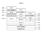
- FIG. 2 is a sectional view of an organic light emitting display device according to the present invention.
- FIGs. 3A to 3C are graphs showing luminescence spectrums according to a maximum photoluminescence peak of a red host of a red emission layer of each of the organic light emitting display devices according to comparative examples and example when a second electrode of each thereof is formed as a transparent electrode and has a thickness of 500 ⁇ ;
- FIG. 4 is an enlarged view of a region of a wavelength of 450 to 575 nm in luminescence spectrums of each of the organic light emitting display devices of comparative examples and example illustrated in FIGs. 3A to 3C ;
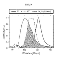
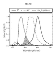
- FIGs. 5A and 5B are images and graphs showing luminescence spectrums according to viewing angle of organic light emitting display devices according to Comparative Example and Example when a second electrode of each organic light emitting display device is a semi-transparent electrode.
- FIG. 2 is a sectional view of an organic light emitting display device according to the present invention.
- the organic light emitting display device includes red, green and blue light emitting cells formed on a substrate 101.
- Each of the red, green and blue light emitting cells includes a first electrode 102, a hole injection layer (HIL) 112, a first hole transport layer (HTL) 114, an emission layer (EML) 110, an electron transport layer (ETL) 116, a second electrode 104, and a front sealing layer 120 that are sequentially formed on the substrate 101.
- each of the red and green light emitting cells further includes a second HTL 118 formed between the first HTL 114 and the EML 110.
- any one of the first and second electrodes 102 and 104 is formed as a semi-transparent electrode and the other thereof is formed as a reflective electrode.
- the organic light emitting display device is of a bottom emission type emitting light downward.
- the second electrode 104 is a semi-transparent electrode and the first electrode 102 is a reflective electrode
- the organic light emitting display device is of a top emission type emitting light upward.
- the first electrode 102 as an anode is formed as a reflective electrode and the second electrode 104 as a cathode is a semi-transparent electrode will be described by way of example.
- the first electrode 102 has a multilayer structure including a metal layer formed of aluminum (Al) or an Al alloy (e.g., AlNd) and a transparent layer formed of indium tin oxide (ITO), indium zinc oxide (IZO), or the like and serves as a reflective electrode.
- Al aluminum
- AlNd Al alloy
- ITO indium tin oxide
- IZO indium zinc oxide
- the second electrode 104 is formed of a single layer or multiple layers, and each layer constituting the second electrode 104 is formed of a metal, an inorganic material, a mixture of metals, a mixture of a metal and an inorganic material, or a mixture thereof.
- a mix ratio of metal to inorganic material is between 10:1 and 1:10.
- a mix ratio of the metals is between 10:1 and 1:10.
- the metal constituting the second electrode 104 may be Ag, Mg, Yb, Li, or Ca and the inorganic material thereof may be Li 2 O, CaO, LiF, or MgF 2 , which assist movement of electrons and thus enable many electrons to be supplied to the EML 110.
- the second electrode 104 has a thickness of 100 to 400 ⁇ and a sheet resistance of 15 ⁇ or less, and the second electrode 104 has a work function of 3.7 to 4.7 eV that is lower than that of the first electrode 102.
- the second electrode 104 has a light transmittance of 30 to 60% at a wavelength of 430 nm, 20 to 50% at a wavelength of 550 nm, and 15 to 40% at a wavelength of 650 nm and thus serves as a semi-transparent electrode.
- the HIL 112 supplies holes from the first electrode 102 to the first and second HTLs 114 and 118.
- the first and second HTLs 114 and 118 supply holes from the HIL 112 to the EML 110 of each light emitting cell.
- the second HTL 118 is not formed in the blue light emitting cell, and the thickness of the second HTL 118 is greater in the red light emitting cell than in the green light emitting cell.
- An efficiency of each light emitting cell in a vertical direction may be optimized through constructive interference of light emitted by adjusting the thickness of the second HTL 118 of each light emitting cell.
- the ETL 116 supplies electrons from the second electrode 104 to the EML 110 of each light emitting cell.
- each of the red (R), green (G) and blue (B) EMLs 110 the holes supplied via the first and second HTLs 114 and 118 and the electrons supplied via the ETL 116 are recombined, thereby generating light.
- the R EML 110 has the greatest thickness
- the B EML 110 has the smallest thickness
- the G EML 110 has a thickness within the range of the thicknesses of the R and B EMLs 110.
- the efficiency of each light emitting cell in a vertical direction may be optimized through constructive interference of light emitted by adjusting the thickness of the EML 110 of each light emitting cell.
- the front sealing layer 120 prevents permeation of external moisture or oxygen and thus enhances reliability.
- the front sealing layer 120 has a structure in which organic layers and inorganic layers are alternately formed several times.
- the inorganic layers are formed of at least one of aluminum oxide (Al x O x ), silicon oxide (SiO x ), SiN x , SiON, and LiF so as to primarily prevent permeation of external moisture or oxygen.
- the organic layers secondarily prevent permeation of external moisture or oxygen.
- the organic layers alleviate stress between the layers according to bending of the organic light emitting display device and enhance planarization performance.
- the organic layers are formed of an acryl-based resin, an epoxy-based resion, or a polymer material such as polyimide or polyethylene.
- the R, G and B EMLs 110 are formed so as to satisfy conditions as shown in Equations 1 to 3 below.
- Equation 1 a difference between a maximum electroluminescent peak (RED EL ⁇ max ) of the R EML 110 and a maximum photoluminescence peak (RH PL ⁇ max ) of a red host included in the R EML 110 is 120 nm or greater.
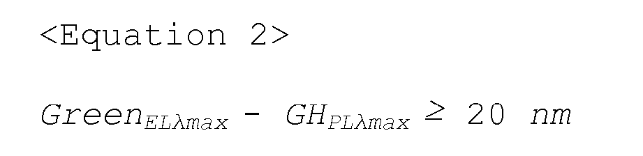
- a difference between a maximum electroluminescent peak (GREEN EL ⁇ max ) of the G EML 110 and a maximum photoluminescence peak (GH PL ⁇ max ) of a green host included in the G EML 110 is 20 nm or greater.
- each of the R, G and B EMLs 110 includes a single host has been described by way of example using Equations 1 to 3.
- each of the R, G and B EMLs 110 includes at least two hosts and, in this case, one of the at least two hosts is formed so as to satisfy the conditions of Equations 1 to 3.
- the electroluminescent peaks refer to maximum values of light emitted when a voltage is applied to the manufactured organic electroluminescent device
- the photoluminescence peaks refer to maximum values of light that represent a characteristic color of each EML.
- the red host has a maximum photoluminescence peak (RH PL ⁇ max ) of 450 to 485 nm and is formed of BAlq 3 series such as a compound represented by Formula 1 below, a material represented by Formula 2 below, or Be complexes such as BeBq 2 represented by Formula 3 below.
- the green host of the G EML 110 has a maximum photoluminescence peak (RH PL ⁇ max ) of 450 to 530 nm and is formed of a material represented by Formula 4 below, BCP series such as a compound represented by Formula 5 below, CBP series such as a compound represented by Formula 6 below, CDBP series, or a material represented by Formula 7 below.
- the blue host of the B EML 110 has a maximum photoluminescence peak (RH PL ⁇ max ) of about 400 to 435 nm and is formed of a material represented by Formula 8 below or an anthracene derivative.
- FIGs. 3A to 3C are graphs showing luminescence spectrums according to a maximum photoluminescence peak of a red host of a red EML of each of the organic light emitting display devices according to comparative examples and example when a second electrode of each thereof is formed as a transparent electrode and has a thickness of 500 ⁇ .
- formation of the second electrode to a thickness of 500 ⁇ is because an out-coupling curve is present around 525 nm, which is the same wavelength as that at a viewing angle of 60 degrees when the second electrode is a semi-transparent electrode and thus the host of the corresponding color emits light around 525 nm.
- a red host included in a red EML is formed of a carbazole derivative having a maximum photoluminescence peak of 490 nm and, in Comparative Example 2 illustrated in FIG. 3B , a red host included in a red EML is formed of a carbazole derivative having a maximum photoluminescence peak of 510 nm.
- an overlapping area between the photoluminescence peak of the red host and a maximum luminescence peak (OC curve) of a red light emitting cell is wide. As the overlapping area increases, amplification between the two peaks increases and thus luminescent strength increases, leading to the greatest change in color according to viewing angle.
- FIGs. 5A and 5B are images and graphs showing luminescence spectrums according to viewing angles of organic light emitting display devices according to Comparative Example and Example when a second electrode of each organic light emitting display device is a semi-transparent electrode.
- a red host included in a red EML is formed of a carbazole derivative having a maximum photoluminescence peak of 510 nm
- a maximum electroluminescent peak (RED EL ⁇ max ) of a red EML is 620 nm and thus a difference between the maximum electroluminescent peak (RED EL ⁇ max ) of a red EML and a maximum photoluminescence peak (RH PL ⁇ max ) of the red host included in the red EML is 110 nm.
- an overlapping area between the electroluminescent peak of the red EML and the photoluminescence peak of the red host at a viewing angle of 0 degrees is relatively wide, and an overlapping area between the electroluminescent peak of the red EML and the photoluminescence peak of the red host at a viewing angle of 60 degrees is relatively wide.
- the overlapping area between the electroluminescent peak of the red EML and the photoluminescence peak of the red host increases, amplification of the electroluminescent peak of the red EML and the photoluminescence peak of the red host increases and thus changes in color occur. Accordingly, there is a difference between colors at viewing angles of 0° and 60°.
- Example illustrated in FIG. 5B when a red host included in a red EML is formed of Be complex series having a maximum photoluminescence peak of 468 nm, a maximum electroluminescent peak (RED EL ⁇ max ) of the red EML 110 is 620 nm and thus a difference between the maximum electroluminescent peak (RED EL ⁇ max ) of the red EML 110 and a maximum photoluminescence peak (RH PL ⁇ max ) of the red host included in the red EML 110 is 152 nm, which is greater than 120 nm.
- an overlapping area between the electroluminescent peak of the red EML 110 and the photoluminescence peak of the red host at a viewing angle of 0° is smaller than that in Comparative Example
- an overlapping area between the electroluminescent peak of the red EML 110 and the photoluminescence peak of the red host at a viewing angle of 60° is smaller than that in Comparative Example.
- the overlapping area between the electroluminescent peak of the red EML 110 and the photoluminescence peak of the red host decreases, amplification of the electroluminescent peak of the red EML 110 and the photoluminescence peak of the red host is relatively small and thus changes in color hardly occur. Accordingly, a difference between colors at viewing angles of 0° and 60° is small and thus color purity according to viewing angle is kept maintained and color purity reliability is enhanced.
- a difference between a maximum electroluminescent peak (RED EL ⁇ max ) of a red EML and a maximum photoluminescence peak (RH PL ⁇ max ) of a red host included in the red EML is 120 nm or greater
- a difference between a maximum electroluminescent peak (GREEN EL ⁇ max ) of a green EML and a maximum photoluminescence peak (GH PL ⁇ max ) of a green host included in the green EML is 20 nm or greater
- a difference between a maximum electroluminescent peak (BLUE EL ⁇ max ) of a blue EML and a maximum photoluminescence peak (BH PL ⁇ max ) of a blue host included in the blue EML is 20 nm or greater. Accordingly, the organic light emitting display device may undergo no reduction in color purity according to viewing angle and suppress host emission, whereby color reliability according to viewing angle may be enhanced.
Landscapes
- Physics & Mathematics (AREA)
- Optics & Photonics (AREA)
- Chemical & Material Sciences (AREA)
- Engineering & Computer Science (AREA)
- Materials Engineering (AREA)
- Inorganic Chemistry (AREA)
- Spectroscopy & Molecular Physics (AREA)
- Electroluminescent Light Sources (AREA)
Abstract



Description
- This application claims the benefit of Korean Patent Application No.
10-2012-0148822, filed on December 18, 2012 - The present invention relates to an organic light emitting display device with enhanced color purity according to viewing angle.
- Organic light emitting display devices, which one form of flat panel display device, are self-emissive devices and have faster response speed, higher luminous efficacy, higher luminance, and wider viewing angle than other flat panel display devices. An organic light emitting display device includes an anode, a cathode facing the anode, and an organic emission layer (EML) disposed therebetween. Holes injected from the anode and electrons injected from the cathode are recombined in the organic EML, forming excitons, which are electron-hole pairs and the excitons return to the ground state, thus releasing energy, whereby light is emitted.
- As a method of enhancing optical efficiency by effectively extracting light emitted from an organic EML, microcavity is used. In a top emission structure, microcavity is based on a principle in which light is repeatedly reflected by a reflective electrode (e.g., an anode) and a semi-transparent electrode (e.g., a cathode) spaced a set distance apart (i.e., an optical path length), and strong interference effects between these light beams occurs and thus light having a particular wavelength is amplified and light having other wavelengths excluding the particular wavelength is eliminated.
- In a microcavity structure, however, an optical path at the front and an optical path at the side differ and thus a wavelength of light that causes resonance is changed. Accordingly, the optical path at the side with a greater viewing angle than that of the front is relatively long and resonance light emitted is shifted towards short wavelengths. That is, as illustrated in
FIG. 1A , a maximum electroluminescent peak of a red light emitting cell is shifted towards short wavelengths by about 75 to 85 nm at a viewing angle of 60° as compared to a viewing angle of 0°, as illustrated inFIG. 1B , a maximum electroluminescent peak of a green light emitting cell is shifted towards short wavelengths by about 36 to 50 nm at a viewing angle of 60° as compared to a viewing angle of 0°, and as illustrated inFIG. 1C , a maximum electroluminescent peak of a blue light emitting cell is shifted towards short wavelengths by about 10 to 14 nm at a viewing angle of 60° as compared to a viewing angle of 0°. This is because, when a non-uniform doping region is formed in an EML, light is emitted by an undoped host. Accordingly, a color shift phenomenon according to viewing angle occurs and thus a conventional organic light emitting display device has reduced reliability in color purity. - Accordingly, the present invention is directed to an organic light emitting display device that substantially obviates one or more problems due to limitations and disadvantages of the related art.
- An object of the present invention is to provide an organic light emitting display device with enhanced color purity according to viewing angle.
- Additional advantages, objects, and features of the invention will be set forth in part in the description which follows and in part will become apparent to those having ordinary skill in the art upon examination of the following or may be learned from practice of the invention. The objectives and other advantages of the invention may be realized and attained by the structure particularly pointed out in the written description and claims hereof as well as the appended drawings.
- To achieve these objects and other advantages and in accordance with the purpose of the invention, as embodied and broadly described herein, an organic light emitting display device includes a first electrode formed on a substrate and being a reflective electrode, a second electrode facing the first electrode and being a semi-transparent electrode, and red, green and blue emission layers formed between the first and second electrodes, wherein a maximum electroluminescent peak of each of the red, green and blue emission layers and a maximum photoluminescence peak of a host included in each emission layer satisfy
Equations 1 to 3 below.


- The second electrode may have a transmittance of 30 to 60% at a wavelength of 430 nm, a transmittance of 20 to 50% at a wavelength of 550 nm, and a transmittance of 15 to 40% at a wavelength of 650 nm, and the second electrode may have a sheet resistance of 1 Ω/□ to 15 Ω/□ and a work function of 3.7 to 4.7 eV.
- The maximum photoluminescence peak of a red host may be between 450 and 485 nm, the maximum photoluminescence peak of a green host may be between 450 and 530 nm, and the maximum photoluminescence peak of a blue host may be between 400 and 435 nm.
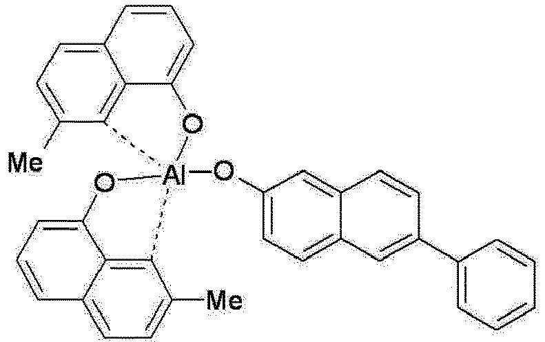
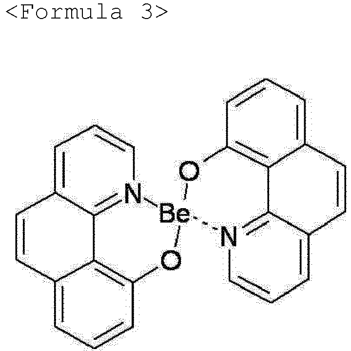
- The red host may be formed of BAlq3 series such as a compound represented by Formula 1 below, a material represented by Formula 2 below, or Be complexes such as BeBq2 represented by Formula 3 below.


- The green host may be formed of a material represented by Formula 4 below, BCP series such as a compound represented by Formula 5 below, CBP series such as a compound represented by Formula 6 below, CDBP series, or a material represented by Formula 7 below.


- The blue host may be formed of a material represented by Formula 8 below or an anthracene derivative.

- The organic light emitting display device may further include a front sealing layer formed on the second electrode, the front sealing layer including organic layers and inorganic layers alternately formed several times.
- The second electrode may have a single layer structure or a multilayer structure and has a total thickness of 100 to 400 Å, and each of the layers of the second electrode may be formed of a metal, an inorganic material, a mixture of metals, a mixture of a metal and an inorganic material, or a mixture thereof. When each layer is formed of the mixture of a metal and an inorganic material, a mix ratio of the metal to the inorganic material may be between 10:1 and 1:10. When each layer is formed of the mixture of metals, a mix ratio of the metals may be between 10:1 and 1:10.
- The metal may be Ag, Mg, Yb, Li, or Ca, and the inorganic material may be LiO2, CaO, LiF, or MgF2.
- It is to be understood that both the foregoing general description and the following detailed description of the present invention are exemplary and explanatory and are intended to provide further explanation of the invention as claimed.
- The accompanying drawings, which are included to provide a further understanding of the invention and are incorporated in and constitute a part of this application, illustrate embodiment(s) of the invention and together with the description serve to explain the principle of the invention. In the drawings:
-
FIG. 1A is a graph showing luminescence spectrums according to viewing angle of a red light emitting cell of a conventional organic light emitting display device; -
FIG. 1B is a graph showing luminescence spectrums according to viewing angle of a green light emitting cell of a conventional organic light emitting display device; -
FIG. 1C is a graph showing luminescence spectrums according to viewing angle of a blue light emitting cell of a conventional organic light emitting display device; -
FIG. 2 is a sectional view of an organic light emitting display device according to the present invention; -
FIGs. 3A to 3C are graphs showing luminescence spectrums according to a maximum photoluminescence peak of a red host of a red emission layer of each of the organic light emitting display devices according to comparative examples and example when a second electrode of each thereof is formed as a transparent electrode and has a thickness of 500 Å; -
FIG. 4 is an enlarged view of a region of a wavelength of 450 to 575 nm in luminescence spectrums of each of the organic light emitting display devices of comparative examples and example illustrated inFIGs. 3A to 3C ; and -
FIGs. 5A and5B are images and graphs showing luminescence spectrums according to viewing angle of organic light emitting display devices according to Comparative Example and Example when a second electrode of each organic light emitting display device is a semi-transparent electrode. - Reference will now be made in detail to the preferred embodiments of the present invention, examples of which are illustrated in the accompanying drawings. Wherever possible, the same reference numbers will be used throughout the drawings to refer to the same or like parts.
- Hereinafter, embodiments of the present invention will be described in detail with reference to the accompanying drawings and the following examples.
-
FIG. 2 is a sectional view of an organic light emitting display device according to the present invention. - As illustrated in
FIG. 2 , the organic light emitting display device includes red, green and blue light emitting cells formed on asubstrate 101. - Each of the red, green and blue light emitting cells includes a
first electrode 102, a hole injection layer (HIL) 112, a first hole transport layer (HTL) 114, an emission layer (EML) 110, an electron transport layer (ETL) 116, asecond electrode 104, and afront sealing layer 120 that are sequentially formed on thesubstrate 101. In addition, each of the red and green light emitting cells further includes asecond HTL 118 formed between thefirst HTL 114 and theEML 110. - Any one of the first and
second electrodes first electrode 102 is a semi-transparent electrode and thesecond electrode 104 is a reflective electrode, the organic light emitting display device is of a bottom emission type emitting light downward. When thesecond electrode 104 is a semi-transparent electrode and thefirst electrode 102 is a reflective electrode, the organic light emitting display device is of a top emission type emitting light upward. In the present invention, a case in which thefirst electrode 102 as an anode is formed as a reflective electrode and thesecond electrode 104 as a cathode is a semi-transparent electrode will be described by way of example. - The
first electrode 102 has a multilayer structure including a metal layer formed of aluminum (Al) or an Al alloy (e.g., AlNd) and a transparent layer formed of indium tin oxide (ITO), indium zinc oxide (IZO), or the like and serves as a reflective electrode. - The
second electrode 104 is formed of a single layer or multiple layers, and each layer constituting thesecond electrode 104 is formed of a metal, an inorganic material, a mixture of metals, a mixture of a metal and an inorganic material, or a mixture thereof. In this regard, when each layer is formed of a metal and an inorganic material, a mix ratio of metal to inorganic material is between 10:1 and 1:10. When each layer is formed of a mixture of metals, a mix ratio of the metals is between 10:1 and 1:10. The metal constituting thesecond electrode 104 may be Ag, Mg, Yb, Li, or Ca and the inorganic material thereof may be Li2O, CaO, LiF, or MgF2, which assist movement of electrons and thus enable many electrons to be supplied to theEML 110. - The
second electrode 104 has a thickness of 100 to 400 Å and a sheet resistance of 15 Ω or less, and thesecond electrode 104 has a work function of 3.7 to 4.7 eV that is lower than that of thefirst electrode 102. - In addition, the
second electrode 104 has a light transmittance of 30 to 60% at a wavelength of 430 nm, 20 to 50% at a wavelength of 550 nm, and 15 to 40% at a wavelength of 650 nm and thus serves as a semi-transparent electrode. - The
HIL 112 supplies holes from thefirst electrode 102 to the first and second HTLs 114 and 118. The first and second HTLs 114 and 118 supply holes from theHIL 112 to theEML 110 of each light emitting cell. Thesecond HTL 118 is not formed in the blue light emitting cell, and the thickness of thesecond HTL 118 is greater in the red light emitting cell than in the green light emitting cell. An efficiency of each light emitting cell in a vertical direction may be optimized through constructive interference of light emitted by adjusting the thickness of thesecond HTL 118 of each light emitting cell. TheETL 116 supplies electrons from thesecond electrode 104 to theEML 110 of each light emitting cell. - In each of the red (R), green (G) and blue (B)
EMLs 110, the holes supplied via the first and second HTLs 114 and 118 and the electrons supplied via theETL 116 are recombined, thereby generating light. In this regard, theR EML 110 has the greatest thickness, theB EML 110 has the smallest thickness, and theG EML 110 has a thickness within the range of the thicknesses of the R andB EMLs 110. The efficiency of each light emitting cell in a vertical direction may be optimized through constructive interference of light emitted by adjusting the thickness of theEML 110 of each light emitting cell. - The
front sealing layer 120 prevents permeation of external moisture or oxygen and thus enhances reliability. For this operation, thefront sealing layer 120 has a structure in which organic layers and inorganic layers are alternately formed several times. The inorganic layers are formed of at least one of aluminum oxide (AlxOx), silicon oxide (SiOx), SiNx, SiON, and LiF so as to primarily prevent permeation of external moisture or oxygen. The organic layers secondarily prevent permeation of external moisture or oxygen. In addition, the organic layers alleviate stress between the layers according to bending of the organic light emitting display device and enhance planarization performance. The organic layers are formed of an acryl-based resin, an epoxy-based resion, or a polymer material such as polyimide or polyethylene. - In the present invention, the R, G and
B EMLs 110 are formed so as to satisfy conditions as shown inEquations 1 to 3 below.


- As shown in
Equation 1, a difference between a maximum electroluminescent peak (REDELλmax) of theR EML 110 and a maximum photoluminescence peak (RHPLλmax) of a red host included in theR EML 110 is 120 nm or greater. As shown inEquation 2, a difference between a maximum electroluminescent peak (GREENELλmax) of theG EML 110 and a maximum photoluminescence peak (GHPLλmax) of a green host included in theG EML 110 is 20 nm or greater. As shown in Equation 3, a difference between a maximum electroluminescent peak (BLUEELλmax) of theB EML 110 and a maximum photoluminescence peak (BHPLλmax) of a blue host included in theB EML 110 is 20 nm or greater. A case in which each of the R, G andB EMLs 110 includes a single host has been described by way ofexample using Equations 1 to 3. In another embodiment, each of the R, G andB EMLs 110 includes at least two hosts and, in this case, one of the at least two hosts is formed so as to satisfy the conditions ofEquations 1 to 3. In addition, inEquations 1 to 3, the electroluminescent peaks refer to maximum values of light emitted when a voltage is applied to the manufactured organic electroluminescent device, and the photoluminescence peaks refer to maximum values of light that represent a characteristic color of each EML. - In
Equation 1, the red host has a maximum photoluminescence peak (RHPLλmax) of 450 to 485 nm and is formed of BAlq3 series such as a compound represented byFormula 1 below, a material represented byFormula 2 below, or Be complexes such as BeBq2 represented by Formula 3 below.


- In
Equation 2, the green host of theG EML 110 has a maximum photoluminescence peak (RHPLλmax) of 450 to 530 nm and is formed of a material represented by Formula 4 below, BCP series such as a compound represented by Formula 5 below, CBP series such as a compound represented by Formula 6 below, CDBP series, or a material represented by Formula 7 below.


- In Equation 3, the blue host of the
B EML 110 has a maximum photoluminescence peak (RHPLλmax) of about 400 to 435 nm and is formed of a material represented by Formula 8 below or an anthracene derivative.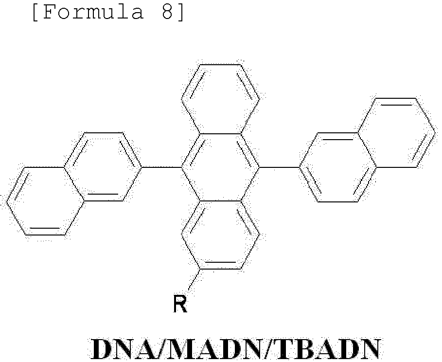
-
FIGs. 3A to 3C are graphs showing luminescence spectrums according to a maximum photoluminescence peak of a red host of a red EML of each of the organic light emitting display devices according to comparative examples and example when a second electrode of each thereof is formed as a transparent electrode and has a thickness of 500 Å. In this regard, formation of the second electrode to a thickness of 500 Å is because an out-coupling curve is present around 525 nm, which is the same wavelength as that at a viewing angle of 60 degrees when the second electrode is a semi-transparent electrode and thus the host of the corresponding color emits light around 525 nm. - In Comparative Example 1 illustrated in
FIG. 3A , a red host included in a red EML is formed of a carbazole derivative having a maximum photoluminescence peak of 490 nm and, in Comparative Example 2 illustrated inFIG. 3B , a red host included in a red EML is formed of a carbazole derivative having a maximum photoluminescence peak of 510 nm. In this case, an overlapping area between the photoluminescence peak of the red host and a maximum luminescence peak (OC curve) of a red light emitting cell is wide. As the overlapping area increases, amplification between the two peaks increases and thus luminescent strength increases, leading to the greatest change in color according to viewing angle. - By contrast, in example illustrated in
FIG. 3C , when a red host is formed of a Be complex derivative having a maximum photoluminescence peak of 468 nm, an overlapping area between the photoluminescence peak of the red host and a maximum luminescence peak (OC curve) of a red light emitting cell is small. As the overlapping area decreases, amplification between the two peaks decreases, which leads to the smallest change in color according to viewing angle. - In addition, in Comparative Example 1 in which the red EML includes the red host formed of a carbazole derivative having a maximum photoluminescence peak of 510 nm and a red dopant, a shoulder peak as illustrated in
FIG. 4 is present at a wavelength of 500 to 550 nm and thus color purity is reduced. By contrast, in example in which an EML includes a red host formed of Be complex series having a maximum photoluminescence peak of 468 nm and a red dopant, a shoulder peak is not present at a wavelength of 500 to 550 nm and thus color purity reliability is enhanced. -
FIGs. 5A and5B are images and graphs showing luminescence spectrums according to viewing angles of organic light emitting display devices according to Comparative Example and Example when a second electrode of each organic light emitting display device is a semi-transparent electrode. - In Comparative Example illustrated in
FIG. 5A , when a red host included in a red EML is formed of a carbazole derivative having a maximum photoluminescence peak of 510 nm, a maximum electroluminescent peak (REDELλmax) of a red EML is 620 nm and thus a difference between the maximum electroluminescent peak (REDELλmax) of a red EML and a maximum photoluminescence peak (RHPLλmax) of the red host included in the red EML is 110 nm. In this case, an overlapping area between the electroluminescent peak of the red EML and the photoluminescence peak of the red host at a viewing angle of 0 degrees is relatively wide, and an overlapping area between the electroluminescent peak of the red EML and the photoluminescence peak of the red host at a viewing angle of 60 degrees is relatively wide. As the overlapping area between the electroluminescent peak of the red EML and the photoluminescence peak of the red host increases, amplification of the electroluminescent peak of the red EML and the photoluminescence peak of the red host increases and thus changes in color occur. Accordingly, there is a difference between colors at viewing angles of 0° and 60°. - By contrast, in Example illustrated in
FIG. 5B , when a red host included in a red EML is formed of Be complex series having a maximum photoluminescence peak of 468 nm, a maximum electroluminescent peak (REDELλmax) of thered EML 110 is 620 nm and thus a difference between the maximum electroluminescent peak (REDELλmax) of thered EML 110 and a maximum photoluminescence peak (RHPLλmax) of the red host included in thered EML 110 is 152 nm, which is greater than 120 nm. In this case, an overlapping area between the electroluminescent peak of thered EML 110 and the photoluminescence peak of the red host at a viewing angle of 0° is smaller than that in Comparative Example, and an overlapping area between the electroluminescent peak of thered EML 110 and the photoluminescence peak of the red host at a viewing angle of 60° is smaller than that in Comparative Example. As the overlapping area between the electroluminescent peak of thered EML 110 and the photoluminescence peak of the red host decreases, amplification of the electroluminescent peak of thered EML 110 and the photoluminescence peak of the red host is relatively small and thus changes in color hardly occur. Accordingly, a difference between colors at viewing angles of 0° and 60° is small and thus color purity according to viewing angle is kept maintained and color purity reliability is enhanced. - As is apparent from the foregoing description, in an organic light emitting display device according to the present invention, a difference between a maximum electroluminescent peak (REDELλmax) of a red EML and a maximum photoluminescence peak (RHPLλmax) of a red host included in the red EML is 120 nm or greater, a difference between a maximum electroluminescent peak (GREENELλmax) of a green EML and a maximum photoluminescence peak (GHPLλmax) of a green host included in the green EML is 20 nm or greater, and a difference between a maximum electroluminescent peak (BLUEELλmax) of a blue EML and a maximum photoluminescence peak (BHPLλmax) of a blue host included in the blue EML is 20 nm or greater. Accordingly, the organic light emitting display device may undergo no reduction in color purity according to viewing angle and suppress host emission, whereby color reliability according to viewing angle may be enhanced.
- It will be apparent to those skilled in the art that various modifications and variations can be made in the present invention without departing from the spirit or scope of the inventions. Thus, it is intended that the present invention covers the modifications and variations of this invention provided they come within the scope of the appended claims and their equivalents.
Claims (9)
- An organic light emitting display device comprising:a first electrode formed on a substrate and being a reflective electrode;a second electrode facing the first electrode and being a semi-transparent electrode; andred, green and blue emission layers formed between the first and second electrodes,wherein a maximum electroluminescent peak of each of the red, green and blue emission layers and a maximum photoluminescence peak of a host included in each emission layer satisfy Equations 1 to 3 below:

wherein REDELλmax is a maximum electroluminescent peak of the red emission layer, and RHPLλmax is a maximum photoluminescence peak of a red host included in the red emission layer,
wherein GREENELλmax is a maximum electroluminescent peak of the green emission layer, and GHPLλmax is a maximum photoluminescence peak of a green host included in the green emission layer, and
wherein BLUEELλmax is a maximum electroluminescent peak of the blue emission layer, and BHPLλmax is a maximum photoluminescence peak of a blue host included in the blue emission layer. - The organic light emitting display device according to claim 1, wherein the second electrode has a transmittance of 30 to 60% at a wavelength of 430 nm, a transmittance of 20 to 50% at a wavelength of 550 nm, and a transmittance of 15 to 40% at a wavelength of 650 nm, and
the second electrode has a sheet resistance of 1 Ω/□ to 15 Ω/□ and a work function of 3.7 to 4.7 eV. - The organic light emitting display device according to claim 1, wherein the maximum photoluminescence peak of a red host is between 450 and 485 nm, the maximum photoluminescence peak of a green host is between 450 and 530 nm, and the maximum photoluminescence peak of a blue host is between 400 and 435 nm.
- The organic light emitting display device according to claim 3, wherein the red host is formed of BAlq3 series such as a compound represented by Formula 1 below, a material represented by Formula 2 below, or Be complexes such as BeBq2 represented by Formula 3 below:


- The organic light emitting display device according to claim 3, wherein the green host is formed of a material represented by Formula 4 below, BCP series such as a compound represented by Formula 5 below, CBP series such as a compound represented by Formula 6 below, CDBP series, or a material represented by Formula 7 below:

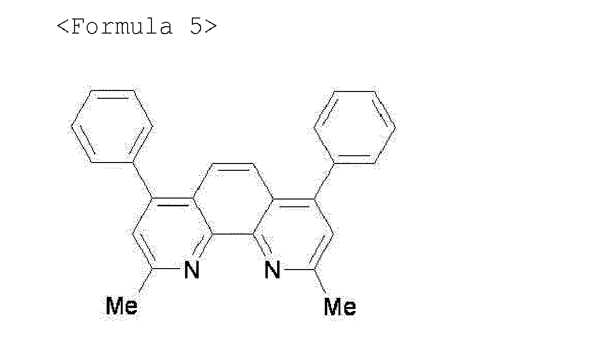


- The organic light emitting display device according to claim 3, wherein the blue host is formed of a material represented by Formula 8 below or an anthracene derivative:

- The organic light emitting display device according to claim 1, further comprising a front sealing layer formed on the second electrode, the front sealing layer comprising organic layers and inorganic layers alternately formed several times.
- The organic light emitting display device according to claim 1, wherein the second electrode has a single layer structure or a multilayer structure and has a total thickness of 100 to 400 Å,
each of the layers of the second electrode being formed of a metal, an inorganic material, a mixture of metals, a mixture of a metal and an inorganic material, or a mixture thereof,
when each layer is formed of the mixture of a metal and an inorganic material, a mix ratio of the metal to the inorganic material being between 10:1 and 1:10, and
when each layer is formed of the mixture of metals, a mix ratio of the metals being between 10:1 and 1:10. - The organic light emitting display device according to claim 8, wherein the metal is Ag, Mg, Yb, Li, or Ca, and the inorganic material is LiO2, CaO, LiF, or MgF2.
Applications Claiming Priority (1)
| Application Number | Priority Date | Filing Date | Title |
|---|---|---|---|
| KR1020120148822A KR101980759B1 (en) | 2012-12-18 | 2012-12-18 | Organic light emitting display |
Publications (3)
| Publication Number | Publication Date |
|---|---|
| EP2747165A2 true EP2747165A2 (en) | 2014-06-25 |
| EP2747165A3 EP2747165A3 (en) | 2015-09-30 |
| EP2747165B1 EP2747165B1 (en) | 2023-08-02 |
Family
ID=49666963
Family Applications (1)
| Application Number | Title | Priority Date | Filing Date |
|---|---|---|---|
| EP13193287.3A Active EP2747165B1 (en) | 2012-12-18 | 2013-11-18 | Organic light emitting display device |
Country Status (4)
| Country | Link |
|---|---|
| US (1) | US9559323B2 (en) |
| EP (1) | EP2747165B1 (en) |
| KR (1) | KR101980759B1 (en) |
| CN (1) | CN103872088B (en) |
Families Citing this family (13)
| Publication number | Priority date | Publication date | Assignee | Title |
|---|---|---|---|---|
| US9570519B2 (en) * | 2014-10-29 | 2017-02-14 | Lg Display Co., Ltd. | Organic light emitting display device with multi-organic layers |
| KR102362839B1 (en) | 2015-10-28 | 2022-02-15 | 삼성디스플레이 주식회사 | Organic light emitting device, fabrication method of the same and organic light emitting display device including the same |
| CN105489632A (en) * | 2016-01-15 | 2016-04-13 | 京东方科技集团股份有限公司 | Organic light-emitting diode (OLED) array substrate, manufacturing method thereof, OLED display panel and OLED display device |
| CN106784363B (en) * | 2016-11-24 | 2018-11-09 | 上海天马有机发光显示技术有限公司 | A kind of organic light emitting display panel, electronic equipment and production method |
| KR102387794B1 (en) * | 2017-10-27 | 2022-04-15 | 엘지디스플레이 주식회사 | White Organic Light Emitting Device and Organic Light Emitting Display Device |
| CN108511628B (en) | 2018-05-16 | 2021-03-02 | 云谷(固安)科技有限公司 | organic electroluminescent device |
| CN108539048B (en) * | 2018-05-16 | 2021-02-12 | 云谷(固安)科技有限公司 | Organic electroluminescent device |
| CN108511618B (en) * | 2018-05-16 | 2021-03-02 | 云谷(固安)科技有限公司 | organic electroluminescent device |
| US11557747B2 (en) * | 2018-11-12 | 2023-01-17 | Wuhan Tianma Micro-Electronics Co., Ltd. | Display device |
| JP7503499B2 (en) * | 2018-12-10 | 2024-06-20 | 株式会社半導体エネルギー研究所 | Light-emitting devices |
| CN110010784B (en) * | 2019-04-09 | 2021-07-13 | 江苏三月科技股份有限公司 | Panchromatic organic electroluminescent device containing multi-channel carrier transmission material |
| KR102776384B1 (en) * | 2020-05-06 | 2025-03-10 | 삼성디스플레이 주식회사 | Llight emitting device and electronic apparatus comprising same |
| KR102836161B1 (en) * | 2021-01-28 | 2025-07-18 | 삼성디스플레이 주식회사 | Light emitting device and electronic apparatus including the same |
Family Cites Families (15)
| Publication number | Priority date | Publication date | Assignee | Title |
|---|---|---|---|---|
| US7755577B2 (en) * | 2005-09-26 | 2010-07-13 | Kyocera Corporation | Electroluminescent device |
| JP4220669B2 (en) * | 2000-12-26 | 2009-02-04 | 出光興産株式会社 | Organic electroluminescence device |
| KR100439648B1 (en) * | 2001-08-29 | 2004-07-12 | 엘지.필립스 엘시디 주식회사 | The organic electro-luminescence device |
| JP2004119304A (en) * | 2002-09-27 | 2004-04-15 | Sanyo Electric Co Ltd | Organic electroluminescence display device and method of manufacturing the same |
| JP4412264B2 (en) * | 2005-09-12 | 2010-02-10 | ソニー株式会社 | Display device and manufacturing method of display device |
| JP2007150191A (en) * | 2005-11-30 | 2007-06-14 | Sanyo Electric Co Ltd | Organic electroluminescence element and organic electroluminescent display device |
| TW200803606A (en) * | 2006-06-13 | 2008-01-01 | Itc Inc Ltd | The fabrication of full color OLED panel using micro-cavity structure |
| JP2008210665A (en) * | 2007-02-27 | 2008-09-11 | Canon Inc | ORGANIC LIGHT EMITTING ELEMENT AND DISPLAY DEVICE USING THE SAME |
| EP2213693A4 (en) * | 2007-11-20 | 2011-11-09 | Idemitsu Kosan Co | POLYMERIC COMPOUND AND ORGANIC ELECTROLUMINESCENT ELEMENT COMPRISING SAME |
| JP2009205928A (en) * | 2008-02-27 | 2009-09-10 | Fuji Electric Holdings Co Ltd | Resonant cavity color conversion el device and organic el display device using the same |
| JP5162554B2 (en) * | 2009-09-25 | 2013-03-13 | パナソニック株式会社 | Organic electroluminescence device |
| KR101752318B1 (en) * | 2010-12-17 | 2017-06-30 | 엘지디스플레이 주식회사 | Method of fabricating Organic electro luminescent device |
| KR101957147B1 (en) * | 2011-06-01 | 2019-03-12 | 엘지디스플레이 주식회사 | Organic electro luminescent device and method of fabricating the same |
| JP6000703B2 (en) * | 2011-08-12 | 2016-10-05 | キヤノン株式会社 | ORGANIC EL ELEMENT, AND LIGHT EMITTING DEVICE, IMAGE FORMING DEVICE, LIGHT EMITTING ELEMENT ARRAY, IMAGING DEVICE, DISPLAY DEVICE USING THE SAME |
| KR101945930B1 (en) * | 2012-01-05 | 2019-02-11 | 삼성디스플레이 주식회사 | Organic light emitting device |
-
2012
- 2012-12-18 KR KR1020120148822A patent/KR101980759B1/en active Active
-
2013
- 2013-11-18 EP EP13193287.3A patent/EP2747165B1/en active Active
- 2013-12-16 CN CN201310688309.XA patent/CN103872088B/en active Active
- 2013-12-17 US US14/109,084 patent/US9559323B2/en active Active
Non-Patent Citations (1)
| Title |
|---|
| None |
Also Published As
| Publication number | Publication date |
|---|---|
| US20140167015A1 (en) | 2014-06-19 |
| KR20140079166A (en) | 2014-06-26 |
| EP2747165B1 (en) | 2023-08-02 |
| CN103872088A (en) | 2014-06-18 |
| CN103872088B (en) | 2018-01-05 |
| KR101980759B1 (en) | 2019-05-21 |
| EP2747165A3 (en) | 2015-09-30 |
| US9559323B2 (en) | 2017-01-31 |
Similar Documents
| Publication | Publication Date | Title |
|---|---|---|
| EP2747165B1 (en) | Organic light emitting display device | |
| US11665918B2 (en) | Organic light emitting device having an optical distance of a micro cavity and method of fabricating the same | |
| EP3038178B1 (en) | Organic electroluminescent device and organic electroluminescent display device | |
| TWI656670B (en) | Organic light-emitting device and organic light-emitting display device using the same | |
| CN103915570B (en) | Organic light emitting display device | |
| US9905788B2 (en) | Organic light emitting display | |
| US9112174B2 (en) | Organic electroluminescent element | |
| CN111403438B (en) | Organic light emitting device | |
| US9666644B2 (en) | Organic electroluminescent element | |
| CN108134012B (en) | Organic light emitting diode, organic light emitting display panel and display device | |
| JP5258166B2 (en) | LIGHT EMITTING ELEMENT, LIGHT EMITTING DEVICE HAVING THE LIGHT EMITTING ELEMENT AND MANUFACTURING METHOD THEREOF | |
| CN106449714A (en) | Organic light-emitting display panel and manufacturing method thereof | |
| KR20220054757A (en) | Organic light emitting element | |
| US20140008631A1 (en) | Organic electroluminescent element | |
| US9203055B2 (en) | Organic light emitting display device and method of manufacturing the same | |
| KR20160038480A (en) | Organic light emitting device | |
| JP4927423B2 (en) | Light emitting device and manufacturing method thereof | |
| CN107768538B (en) | Organic Light Emitting Diode | |
| KR102228477B1 (en) | Organic light emitting device | |
| KR102358545B1 (en) | Organic light emitting display device | |
| KR20160061718A (en) | Organic light emitting device | |
| KR20150125159A (en) | White organic light emitting device |
Legal Events
| Date | Code | Title | Description |
|---|---|---|---|
| PUAI | Public reference made under article 153(3) epc to a published international application that has entered the european phase |
Free format text: ORIGINAL CODE: 0009012 |
|
| 17P | Request for examination filed |
Effective date: 20131118 |
|
| AK | Designated contracting states |
Kind code of ref document: A2 Designated state(s): AL AT BE BG CH CY CZ DE DK EE ES FI FR GB GR HR HU IE IS IT LI LT LU LV MC MK MT NL NO PL PT RO RS SE SI SK SM TR |
|
| AX | Request for extension of the european patent |
Extension state: BA ME |
|
| PUAL | Search report despatched |
Free format text: ORIGINAL CODE: 0009013 |
|
| AK | Designated contracting states |
Kind code of ref document: A3 Designated state(s): AL AT BE BG CH CY CZ DE DK EE ES FI FR GB GR HR HU IE IS IT LI LT LU LV MC MK MT NL NO PL PT RO RS SE SI SK SM TR |
|
| AX | Request for extension of the european patent |
Extension state: BA ME |
|
| RIC1 | Information provided on ipc code assigned before grant |
Ipc: H01L 51/52 20060101AFI20150821BHEP Ipc: H01L 51/50 20060101ALN20150821BHEP Ipc: H01L 51/54 20060101ALI20150821BHEP Ipc: H01L 27/32 20060101ALN20150821BHEP |
|
| STAA | Information on the status of an ep patent application or granted ep patent |
Free format text: STATUS: EXAMINATION IS IN PROGRESS |
|
| 17Q | First examination report despatched |
Effective date: 20190125 |
|
| REG | Reference to a national code |
Ref country code: DE Ref legal event code: R079 Free format text: PREVIOUS MAIN CLASS: H01L0051520000 Ipc: H10K0059350000 Ref document number: 602013084356 Country of ref document: DE |
|
| GRAP | Despatch of communication of intention to grant a patent |
Free format text: ORIGINAL CODE: EPIDOSNIGR1 |
|
| STAA | Information on the status of an ep patent application or granted ep patent |
Free format text: STATUS: GRANT OF PATENT IS INTENDED |
|
| RIC1 | Information provided on ipc code assigned before grant |
Ipc: H10K 50/852 20230101ALI20230207BHEP Ipc: H10K 85/30 20230101ALI20230207BHEP Ipc: H10K 85/60 20230101ALI20230207BHEP Ipc: H10K 50/11 20230101ALI20230207BHEP Ipc: H10K 59/35 20230101AFI20230207BHEP |
|
| INTG | Intention to grant announced |
Effective date: 20230224 |
|
| RIN1 | Information on inventor provided before grant (corrected) |
Inventor name: LEE, SEOK-JONG Inventor name: KIM, KWAN-SOO Inventor name: LEE, SE-HEE Inventor name: KWON, SUN-KAP Inventor name: PARK, JIN-HO |
|
| GRAS | Grant fee paid |
Free format text: ORIGINAL CODE: EPIDOSNIGR3 |
|
| GRAA | (expected) grant |
Free format text: ORIGINAL CODE: 0009210 |
|
| STAA | Information on the status of an ep patent application or granted ep patent |
Free format text: STATUS: THE PATENT HAS BEEN GRANTED |
|
| AK | Designated contracting states |
Kind code of ref document: B1 Designated state(s): AL AT BE BG CH CY CZ DE DK EE ES FI FR GB GR HR HU IE IS IT LI LT LU LV MC MK MT NL NO PL PT RO RS SE SI SK SM TR |
|
| REG | Reference to a national code |
Ref country code: GB Ref legal event code: FG4D |
|
| REG | Reference to a national code |
Ref country code: CH Ref legal event code: EP |
|
| REG | Reference to a national code |
Ref country code: DE Ref legal event code: R096 Ref document number: 602013084356 Country of ref document: DE |
|
| REG | Reference to a national code |
Ref country code: IE Ref legal event code: FG4D |
|
| REG | Reference to a national code |
Ref country code: LT Ref legal event code: MG9D |
|
| REG | Reference to a national code |
Ref country code: NL Ref legal event code: MP Effective date: 20230802 |
|
| REG | Reference to a national code |
Ref country code: AT Ref legal event code: MK05 Ref document number: 1596344 Country of ref document: AT Kind code of ref document: T Effective date: 20230802 |
|
| PG25 | Lapsed in a contracting state [announced via postgrant information from national office to epo] |
Ref country code: GR Free format text: LAPSE BECAUSE OF FAILURE TO SUBMIT A TRANSLATION OF THE DESCRIPTION OR TO PAY THE FEE WITHIN THE PRESCRIBED TIME-LIMIT Effective date: 20231103 |
|
| PG25 | Lapsed in a contracting state [announced via postgrant information from national office to epo] |
Ref country code: IS Free format text: LAPSE BECAUSE OF FAILURE TO SUBMIT A TRANSLATION OF THE DESCRIPTION OR TO PAY THE FEE WITHIN THE PRESCRIBED TIME-LIMIT Effective date: 20231202 |
|
| PG25 | Lapsed in a contracting state [announced via postgrant information from national office to epo] |
Ref country code: SE Free format text: LAPSE BECAUSE OF FAILURE TO SUBMIT A TRANSLATION OF THE DESCRIPTION OR TO PAY THE FEE WITHIN THE PRESCRIBED TIME-LIMIT Effective date: 20230802 Ref country code: RS Free format text: LAPSE BECAUSE OF FAILURE TO SUBMIT A TRANSLATION OF THE DESCRIPTION OR TO PAY THE FEE WITHIN THE PRESCRIBED TIME-LIMIT Effective date: 20230802 Ref country code: PT Free format text: LAPSE BECAUSE OF FAILURE TO SUBMIT A TRANSLATION OF THE DESCRIPTION OR TO PAY THE FEE WITHIN THE PRESCRIBED TIME-LIMIT Effective date: 20231204 Ref country code: NO Free format text: LAPSE BECAUSE OF FAILURE TO SUBMIT A TRANSLATION OF THE DESCRIPTION OR TO PAY THE FEE WITHIN THE PRESCRIBED TIME-LIMIT Effective date: 20231102 Ref country code: NL Free format text: LAPSE BECAUSE OF FAILURE TO SUBMIT A TRANSLATION OF THE DESCRIPTION OR TO PAY THE FEE WITHIN THE PRESCRIBED TIME-LIMIT Effective date: 20230802 Ref country code: LV Free format text: LAPSE BECAUSE OF FAILURE TO SUBMIT A TRANSLATION OF THE DESCRIPTION OR TO PAY THE FEE WITHIN THE PRESCRIBED TIME-LIMIT Effective date: 20230802 Ref country code: LT Free format text: LAPSE BECAUSE OF FAILURE TO SUBMIT A TRANSLATION OF THE DESCRIPTION OR TO PAY THE FEE WITHIN THE PRESCRIBED TIME-LIMIT Effective date: 20230802 Ref country code: IS Free format text: LAPSE BECAUSE OF FAILURE TO SUBMIT A TRANSLATION OF THE DESCRIPTION OR TO PAY THE FEE WITHIN THE PRESCRIBED TIME-LIMIT Effective date: 20231202 Ref country code: HR Free format text: LAPSE BECAUSE OF FAILURE TO SUBMIT A TRANSLATION OF THE DESCRIPTION OR TO PAY THE FEE WITHIN THE PRESCRIBED TIME-LIMIT Effective date: 20230802 Ref country code: GR Free format text: LAPSE BECAUSE OF FAILURE TO SUBMIT A TRANSLATION OF THE DESCRIPTION OR TO PAY THE FEE WITHIN THE PRESCRIBED TIME-LIMIT Effective date: 20231103 Ref country code: FI Free format text: LAPSE BECAUSE OF FAILURE TO SUBMIT A TRANSLATION OF THE DESCRIPTION OR TO PAY THE FEE WITHIN THE PRESCRIBED TIME-LIMIT Effective date: 20230802 Ref country code: AT Free format text: LAPSE BECAUSE OF FAILURE TO SUBMIT A TRANSLATION OF THE DESCRIPTION OR TO PAY THE FEE WITHIN THE PRESCRIBED TIME-LIMIT Effective date: 20230802 |
|
| PG25 | Lapsed in a contracting state [announced via postgrant information from national office to epo] |
Ref country code: PL Free format text: LAPSE BECAUSE OF FAILURE TO SUBMIT A TRANSLATION OF THE DESCRIPTION OR TO PAY THE FEE WITHIN THE PRESCRIBED TIME-LIMIT Effective date: 20230802 |
|
| PG25 | Lapsed in a contracting state [announced via postgrant information from national office to epo] |
Ref country code: ES Free format text: LAPSE BECAUSE OF FAILURE TO SUBMIT A TRANSLATION OF THE DESCRIPTION OR TO PAY THE FEE WITHIN THE PRESCRIBED TIME-LIMIT Effective date: 20230802 |
|
| PG25 | Lapsed in a contracting state [announced via postgrant information from national office to epo] |
Ref country code: SM Free format text: LAPSE BECAUSE OF FAILURE TO SUBMIT A TRANSLATION OF THE DESCRIPTION OR TO PAY THE FEE WITHIN THE PRESCRIBED TIME-LIMIT Effective date: 20230802 Ref country code: RO Free format text: LAPSE BECAUSE OF FAILURE TO SUBMIT A TRANSLATION OF THE DESCRIPTION OR TO PAY THE FEE WITHIN THE PRESCRIBED TIME-LIMIT Effective date: 20230802 Ref country code: ES Free format text: LAPSE BECAUSE OF FAILURE TO SUBMIT A TRANSLATION OF THE DESCRIPTION OR TO PAY THE FEE WITHIN THE PRESCRIBED TIME-LIMIT Effective date: 20230802 Ref country code: EE Free format text: LAPSE BECAUSE OF FAILURE TO SUBMIT A TRANSLATION OF THE DESCRIPTION OR TO PAY THE FEE WITHIN THE PRESCRIBED TIME-LIMIT Effective date: 20230802 Ref country code: DK Free format text: LAPSE BECAUSE OF FAILURE TO SUBMIT A TRANSLATION OF THE DESCRIPTION OR TO PAY THE FEE WITHIN THE PRESCRIBED TIME-LIMIT Effective date: 20230802 Ref country code: CZ Free format text: LAPSE BECAUSE OF FAILURE TO SUBMIT A TRANSLATION OF THE DESCRIPTION OR TO PAY THE FEE WITHIN THE PRESCRIBED TIME-LIMIT Effective date: 20230802 Ref country code: SK Free format text: LAPSE BECAUSE OF FAILURE TO SUBMIT A TRANSLATION OF THE DESCRIPTION OR TO PAY THE FEE WITHIN THE PRESCRIBED TIME-LIMIT Effective date: 20230802 |
|
| REG | Reference to a national code |
Ref country code: DE Ref legal event code: R097 Ref document number: 602013084356 Country of ref document: DE |
|
| PG25 | Lapsed in a contracting state [announced via postgrant information from national office to epo] |
Ref country code: IT Free format text: LAPSE BECAUSE OF FAILURE TO SUBMIT A TRANSLATION OF THE DESCRIPTION OR TO PAY THE FEE WITHIN THE PRESCRIBED TIME-LIMIT Effective date: 20230802 |
|
| PLBE | No opposition filed within time limit |
Free format text: ORIGINAL CODE: 0009261 |
|
| STAA | Information on the status of an ep patent application or granted ep patent |
Free format text: STATUS: NO OPPOSITION FILED WITHIN TIME LIMIT |
|
| REG | Reference to a national code |
Ref country code: CH Ref legal event code: PL |
|
| PG25 | Lapsed in a contracting state [announced via postgrant information from national office to epo] |
Ref country code: MC Free format text: LAPSE BECAUSE OF FAILURE TO SUBMIT A TRANSLATION OF THE DESCRIPTION OR TO PAY THE FEE WITHIN THE PRESCRIBED TIME-LIMIT Effective date: 20230802 |
|
| 26N | No opposition filed |
Effective date: 20240503 |
|
| PG25 | Lapsed in a contracting state [announced via postgrant information from national office to epo] |
Ref country code: LU Free format text: LAPSE BECAUSE OF NON-PAYMENT OF DUE FEES Effective date: 20231118 |
|
| PG25 | Lapsed in a contracting state [announced via postgrant information from national office to epo] |
Ref country code: CH Free format text: LAPSE BECAUSE OF NON-PAYMENT OF DUE FEES Effective date: 20231130 |
|
| PG25 | Lapsed in a contracting state [announced via postgrant information from national office to epo] |
Ref country code: MC Free format text: LAPSE BECAUSE OF FAILURE TO SUBMIT A TRANSLATION OF THE DESCRIPTION OR TO PAY THE FEE WITHIN THE PRESCRIBED TIME-LIMIT Effective date: 20230802 Ref country code: LU Free format text: LAPSE BECAUSE OF NON-PAYMENT OF DUE FEES Effective date: 20231118 Ref country code: CH Free format text: LAPSE BECAUSE OF NON-PAYMENT OF DUE FEES Effective date: 20231130 Ref country code: SI Free format text: LAPSE BECAUSE OF FAILURE TO SUBMIT A TRANSLATION OF THE DESCRIPTION OR TO PAY THE FEE WITHIN THE PRESCRIBED TIME-LIMIT Effective date: 20230802 |
|
| REG | Reference to a national code |
Ref country code: BE Ref legal event code: MM Effective date: 20231130 |
|
| REG | Reference to a national code |
Ref country code: IE Ref legal event code: MM4A |
|
| PG25 | Lapsed in a contracting state [announced via postgrant information from national office to epo] |
Ref country code: IE Free format text: LAPSE BECAUSE OF NON-PAYMENT OF DUE FEES Effective date: 20231118 |
|
| PG25 | Lapsed in a contracting state [announced via postgrant information from national office to epo] |
Ref country code: BE Free format text: LAPSE BECAUSE OF NON-PAYMENT OF DUE FEES Effective date: 20231130 |
|
| PG25 | Lapsed in a contracting state [announced via postgrant information from national office to epo] |
Ref country code: IE Free format text: LAPSE BECAUSE OF NON-PAYMENT OF DUE FEES Effective date: 20231118 Ref country code: BE Free format text: LAPSE BECAUSE OF NON-PAYMENT OF DUE FEES Effective date: 20231130 |
|
| PG25 | Lapsed in a contracting state [announced via postgrant information from national office to epo] |
Ref country code: BG Free format text: LAPSE BECAUSE OF FAILURE TO SUBMIT A TRANSLATION OF THE DESCRIPTION OR TO PAY THE FEE WITHIN THE PRESCRIBED TIME-LIMIT Effective date: 20230802 |
|
| PG25 | Lapsed in a contracting state [announced via postgrant information from national office to epo] |
Ref country code: BG Free format text: LAPSE BECAUSE OF FAILURE TO SUBMIT A TRANSLATION OF THE DESCRIPTION OR TO PAY THE FEE WITHIN THE PRESCRIBED TIME-LIMIT Effective date: 20230802 |
|
| PG25 | Lapsed in a contracting state [announced via postgrant information from national office to epo] |
Ref country code: CY Free format text: LAPSE BECAUSE OF FAILURE TO SUBMIT A TRANSLATION OF THE DESCRIPTION OR TO PAY THE FEE WITHIN THE PRESCRIBED TIME-LIMIT; INVALID AB INITIO Effective date: 20131118 |
|
| PG25 | Lapsed in a contracting state [announced via postgrant information from national office to epo] |
Ref country code: HU Free format text: LAPSE BECAUSE OF FAILURE TO SUBMIT A TRANSLATION OF THE DESCRIPTION OR TO PAY THE FEE WITHIN THE PRESCRIBED TIME-LIMIT; INVALID AB INITIO Effective date: 20131118 |
|
| PGFP | Annual fee paid to national office [announced via postgrant information from national office to epo] |
Ref country code: GB Payment date: 20250922 Year of fee payment: 13 |
|
| PGFP | Annual fee paid to national office [announced via postgrant information from national office to epo] |
Ref country code: FR Payment date: 20250925 Year of fee payment: 13 |
|
| PG25 | Lapsed in a contracting state [announced via postgrant information from national office to epo] |
Ref country code: TR Free format text: LAPSE BECAUSE OF FAILURE TO SUBMIT A TRANSLATION OF THE DESCRIPTION OR TO PAY THE FEE WITHIN THE PRESCRIBED TIME-LIMIT Effective date: 20230802 |
|
| PGFP | Annual fee paid to national office [announced via postgrant information from national office to epo] |
Ref country code: DE Payment date: 20250922 Year of fee payment: 13 |