EP2747120A1 - Method of smoothing solid surface with gas cluster ion beam and solid surface smoothing apparatus - Google Patents
Method of smoothing solid surface with gas cluster ion beam and solid surface smoothing apparatus Download PDFInfo
- Publication number
- EP2747120A1 EP2747120A1 EP14160257.3A EP14160257A EP2747120A1 EP 2747120 A1 EP2747120 A1 EP 2747120A1 EP 14160257 A EP14160257 A EP 14160257A EP 2747120 A1 EP2747120 A1 EP 2747120A1
- Authority
- EP
- European Patent Office
- Prior art keywords
- ion beam
- cluster ion
- gas cluster
- solid surface
- irradiation
- Prior art date
- Legal status (The legal status is an assumption and is not a legal conclusion. Google has not performed a legal analysis and makes no representation as to the accuracy of the status listed.)
- Granted
Links
Images



Classifications
-
- C—CHEMISTRY; METALLURGY
- C23—COATING METALLIC MATERIAL; COATING MATERIAL WITH METALLIC MATERIAL; CHEMICAL SURFACE TREATMENT; DIFFUSION TREATMENT OF METALLIC MATERIAL; COATING BY VACUUM EVAPORATION, BY SPUTTERING, BY ION IMPLANTATION OR BY CHEMICAL VAPOUR DEPOSITION, IN GENERAL; INHIBITING CORROSION OF METALLIC MATERIAL OR INCRUSTATION IN GENERAL
- C23F—NON-MECHANICAL REMOVAL OF METALLIC MATERIAL FROM SURFACE; INHIBITING CORROSION OF METALLIC MATERIAL OR INCRUSTATION IN GENERAL; MULTI-STEP PROCESSES FOR SURFACE TREATMENT OF METALLIC MATERIAL INVOLVING AT LEAST ONE PROCESS PROVIDED FOR IN CLASS C23 AND AT LEAST ONE PROCESS COVERED BY SUBCLASS C21D OR C22F OR CLASS C25
- C23F4/00—Processes for removing metallic material from surfaces, not provided for in group C23F1/00 or C23F3/00
-
- H—ELECTRICITY
- H10—SEMICONDUCTOR DEVICES; ELECTRIC SOLID-STATE DEVICES NOT OTHERWISE PROVIDED FOR
- H10P—GENERIC PROCESSES OR APPARATUS FOR THE MANUFACTURE OR TREATMENT OF DEVICES COVERED BY CLASS H10
- H10P50/00—Etching of wafers, substrates or parts of devices
-
- H—ELECTRICITY
- H01—ELECTRIC ELEMENTS
- H01J—ELECTRIC DISCHARGE TUBES OR DISCHARGE LAMPS
- H01J27/00—Ion beam tubes
- H01J27/02—Ion sources; Ion guns
- H01J27/026—Cluster ion sources
-
- H—ELECTRICITY
- H01—ELECTRIC ELEMENTS
- H01J—ELECTRIC DISCHARGE TUBES OR DISCHARGE LAMPS
- H01J37/00—Discharge tubes with provision for introducing objects or material to be exposed to the discharge, e.g. for the purpose of examination or processing thereof
- H01J37/02—Details
- H01J37/20—Means for supporting or positioning the object or the material; Means for adjusting diaphragms or lenses associated with the support
-
- H—ELECTRICITY
- H01—ELECTRIC ELEMENTS
- H01J—ELECTRIC DISCHARGE TUBES OR DISCHARGE LAMPS
- H01J37/00—Discharge tubes with provision for introducing objects or material to be exposed to the discharge, e.g. for the purpose of examination or processing thereof
- H01J37/30—Electron-beam or ion-beam tubes for localised treatment of objects
- H01J37/305—Electron-beam or ion-beam tubes for localised treatment of objects for casting, melting, evaporating, or etching
- H01J37/3053—Electron-beam or ion-beam tubes for localised treatment of objects for casting, melting, evaporating, or etching for evaporating or etching
-
- H—ELECTRICITY
- H01—ELECTRIC ELEMENTS
- H01J—ELECTRIC DISCHARGE TUBES OR DISCHARGE LAMPS
- H01J37/00—Discharge tubes with provision for introducing objects or material to be exposed to the discharge, e.g. for the purpose of examination or processing thereof
- H01J37/30—Electron-beam or ion-beam tubes for localised treatment of objects
- H01J37/317—Electron-beam or ion-beam tubes for localised treatment of objects for changing properties of the objects or for applying thin layers thereon, e.g. for ion implantation
-
- H—ELECTRICITY
- H01—ELECTRIC ELEMENTS
- H01J—ELECTRIC DISCHARGE TUBES OR DISCHARGE LAMPS
- H01J2237/00—Discharge tubes exposing object to beam, e.g. for analysis treatment, etching, imaging
- H01J2237/20—Positioning, supporting, modifying or maintaining the physical state of objects being observed or treated
- H01J2237/202—Movement
- H01J2237/20207—Tilt
-
- H—ELECTRICITY
- H01—ELECTRIC ELEMENTS
- H01J—ELECTRIC DISCHARGE TUBES OR DISCHARGE LAMPS
- H01J2237/00—Discharge tubes exposing object to beam, e.g. for analysis treatment, etching, imaging
- H01J2237/20—Positioning, supporting, modifying or maintaining the physical state of objects being observed or treated
- H01J2237/202—Movement
- H01J2237/20214—Rotation
-
- H—ELECTRICITY
- H10—SEMICONDUCTOR DEVICES; ELECTRIC SOLID-STATE DEVICES NOT OTHERWISE PROVIDED FOR
- H10P—GENERIC PROCESSES OR APPARATUS FOR THE MANUFACTURE OR TREATMENT OF DEVICES COVERED BY CLASS H10
- H10P50/00—Etching of wafers, substrates or parts of devices
- H10P50/20—Dry etching; Plasma etching; Reactive-ion etching
- H10P50/24—Dry etching; Plasma etching; Reactive-ion etching of semiconductor materials
- H10P50/242—Dry etching; Plasma etching; Reactive-ion etching of semiconductor materials of Group IV materials
Definitions
- the present invention relates to a method of smoothing a solid surface by gas cluster ion beam irradiation and to an apparatus therefor.
- Patent literature 1 smoothes a substrate surface by sputtering using monatomic or monomolecular ions of Ar (argon) gas directed onto the substrate surface at a low angle.
- Ar Ar
- Patent literature 2 discloses a method of reducing surface roughness by irradiating a solid surface with a gas cluster ion beam.
- gas cluster ions directed onto the workpiece (solid) dissociate when they collide with the workpiece.
- multibody collisions arise between atoms or molecules forming the cluster and atoms or molecules forming the workpiece, causing noticeable motion in a lateral direction with respect to the workpiece surface (solid surface).
- the workpiece surface is cut laterally. This phenomenon is called lateral sputtering.
- the motion of particles in a lateral direction with respect to the workpiece surface mainly cuts projecting portions from the surface, performing ultraprecise polishing to produce a smooth surface at the atomic level.
- an ion has a lower energy than that in normal ion etching. In other words, a single atom or molecule forming the cluster has a lower energy. This enables ultraprecise polishing as needed, without damaging the workpiece surface.
- One advantage of solid surface smoothing using a gas cluster ion beam is that the damage to the workpiece surface is less than that caused by ion etching, which is disclosed in Patent literature 1.
- Patent literature 2 discloses that a curved surface or the like may be irradiated in an oblique direction, depending on the surface condition, but the effect of such oblique irradiation is not mentioned. Therefore, Patent literature 2 implies that approximately perpendicular irradiation of the solid surface is the most efficient for surface smoothing.
- Patent literature 3 discloses another example of solid surface smoothing by using a gas cluster ion beam. However, Patent literature 3 does not describe the relationship between surface smoothing and the angle formed by the gas cluster ion beam and the solid surface. Since the description indicates that the lateral sputtering effect is used, it is inferred that, like Patent literature 2, Patent literature 3 shows data for perpendicular irradiation.
- Non-patent literature 1 also includes a report of solid surface smoothing by gas cluster ion beam irradiation.
- Toyoda and others report that surface roughness is reduced by irradiating the surface of materials such as Cu, SiC, and GaN with Ar cluster ions. The surface was irradiated with the gas cluster ion beam at approximately right angles.
- Non-patent literature 2 describes variations in the roughness of a solid surface when the solid surface is irradiated with a gas cluster ion beam at a variety of irradiation angles.
- the irradiation angle is expressed as 90 degrees (the symbol ° will be used hereafter to express an angle).
- the irradiation angle is expressed as 0°.
- the literature discloses that the sputtering rate, which indicates a speed at which the surface is etched, is maximized by perpendicular irradiation and that the etching rate decreases as the irradiation angle decreases.
- Patent literature 4 describes the use of a plurality of irradiation angles in irradiation of the solid surface with the gas cluster ion beam. In patent literature 4, the irradiation is performed at different angles in succession.
- sputtering is performed by emitting an ion beam of Ar (argon) gas or the like, and projecting portions are cut off from the solid surface with priority.
- Ar Ar
- the irradiation energy must be kept below 100 eV or so, in order to suppress damage to the solid surface. In that case, an extremely small ion current cannot provide a practical sputtering rate.
- the smoothing method disclosed in Patent literature 1 has a serious problem in that smoothing is almost impossible if the solid surface has a scratch or other surface roughness having a submicrometer (0.1 ⁇ m to 1 ⁇ m) to micrometer ( ⁇ m) width and height.
- an object of the present invention is to provide a solid surface smoothing method and apparatus that can reduce surface roughness like a scratch in solid surface by gas cluster ion beam irradiation.
- the present invention provides a method of smoothing a solid surface with a gas cluster ion beam and an apparatus for smoothing a solid surface with a gas cluster ion beam having the features of the respective independent claims. Preferred embodiments of the invention are described in the dependent claims.
- a method of smoothing a solid surface with a gas cluster ion beam includes an irradiation step of irradiating a solid surface with a gas cluster ion beam, and the irradiation step includes a process of causing clusters from a plurality of directions to collide with at least an area (spot) irradiated with the gas cluster ion beam on the solid surface. Upon collision of the clusters coming from a plurality of directions with the spot, the individual clusters advance sputtering in various directions.
- the collision of the clusters coming from a plurality of directions with the spot may be performed by an irradiation of the gas cluster ion beam in which flight directions of the clusters diverge with respect to a center of the beam. It is preferred that the gas cluster ion beam be a gas cluster ion beam randomly diverging with an angle of at least 2° with respect to the center of the beam.
- the collision of the clusters coming from a plurality of directions with the spot may also be performed by emitting the gas cluster ion beam while moving the solid.
- clusters can collide with the spot from more directions.
- the collision of the clusters coming from a plurality of directions with the spot may be performed by emitting the gas cluster ion beam while rotating the solid.
- clusters can collide with the spot from more directions.
- the collision of the clusters from a plurality of directions with the spot may be performed by emitting the gas cluster ion beam while keeping the irradiation angle formed by the gas cluster ion beam and the normal to the solid surface mismatched.
- the collision of the clusters coming from a plurality of directions with the spot may be performed by emitting one or more gas cluster ion beams in addition to the emission of the gas cluster ion beam.
- clusters can collide with the spot from more directions.
- a solid surface smoothing apparatus for smoothing a solid surface with a gas cluster ion beam includes a beam setup means adapted to set up the gas cluster ion beam to diverge randomly with an angle of at least 2° with respect to a center of the beam, a gas cluster ion beam emission means which emits the gas cluster ion beam onto the solid surface, and a means adapted to move the solid and/or a means adapted to rotate the solid.
- a plurality of gas cluster ion beam emission means may be included.
- the spot which is a gas cluster ion beam irradiation area
- sputtering proceeds in various directions with the individual clusters. In this process, scratches or similar surface roughness in the solid surface can be reduced.
- Fig. 1A is a diagram illustrating how a solid surface is smoothed out by lateral sputtering.
- the inventors observed smoothing of a solid surface having scratches or the like with widths and heights on the order of a submicrometer to micrometer.
- GCIB irradiation was performed by likening a line-and-space pattern structure 900 to a scratch.
- a surface having scratches was hardly smoothed by the conventional lateral sputtering. This state is illustrated in Fig. 1B .
- the reason for failure of smoothing is that both the top of the line denoted by a reference numeral 901 (a part around the top of a projecting portion of the line-and-space pattern structure, corresponding to a projection) and the bottom of the space denoted by a reference numeral 902 (a part around the bottom of a grooved portion in the line-and-space pattern structure, corresponding to a recess) in the line-and-space pattern structure 900 were etched, making little difference in height. In other words, because etching proceeds analogously to the original shape of the surface, little smoothing arose.
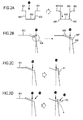
- Figs. 2A to 2D are diagrams showing the states. As shown in Fig. 2A , the phenomenon was observed that the GCIB irradiation had caused a substance 904 around the top of the line to move along the side wall 903 of the line to the lower part of the side wall of the line denoted by a reference numeral 905 (a part of the side wall 903 in the depth direction of the line, far from the top 901 of the line).
- the observed transfer is indicated by a broken arrow in the right diagram in Fig. 2A .
- a shoulder-like part denoted by a reference numeral 907 (enclosed with a broken line in Fig. 2B ) was observed on the edge of the line (near the border between the top 901 of the line and the side wall 903 of the line).
- the right diagram in Fig. 2B is an enlarged view of a circled part 906 in the left diagram of Fig. 2B .
- a broken arrow represents the lateral movement of a substance near the top of the line.
- a reference numeral 908 denotes a substance near the top of the line
- a reference numeral 909 denotes a substance moved along the side wall 903 of the line.
- the substance near the top of the line does not move to a wide area across the bottom of the space. Therefore, both the top of the line and the bottom of the space are etched, making little difference in height.
- the inventors have found the following: To reduce (smooth out) scratches or similar surface roughness by GCIB irradiation, it is important to expose a substance in the solid surface transferred laterally by a collision with clusters to other clusters (or to repeat collision); this should be achieved by making a spot of a GCIB irradiation area collided with clusters coming from a plurality of directions; to promote substance transfer over a wider range for the purpose of achieving maximum smoothing of the solid surface, time intervals between cluster collisions should be minimized so that the clusters collide almost at the same time.
- Clusters coming from a plurality of directions should be collided with the area (spot) irradiated by the GCIB.
- spot irradiated by the GCIB.
- roughly simultaneous cluster collisions should be caused to promote smoothing of the solid surface.
- GCIB emission means is structured as follows.
- Source gas 9 is supplied via a nozzle 10 into a vacuum cluster generation chamber 11.
- Gas molecules of the source gas 9 aggregate into clusters in the cluster generation chamber 11.
- the cluster size is determined by the particle size distribution based on the pressure and temperature of gas at a nozzle outlet 10a and the size and shape of the nozzle 10.
- the clusters generated in the cluster generation chamber 11 are guided into an ionization chamber 13 by a skimmer 12 as a gas cluster beam.
- a skimmer diameter of the skimmer 12 By increasing the skimmer diameter of the skimmer 12, a relatively random mixture of beams having different angles can be produced, instead of GCIBs diverging concentrically and uniformly.
- an ionizer 14 emits an electron beam of thermal electrons, for example, to ionize the neutral clusters.
- the ionized gas cluster beam (GCIB) is accelerated by an accelerating electrode 15.
- GCIB gas cluster beam
- a magnetic-field convergence control unit 16 to produce a nondivergent GCIB, beams are converged into parallel beams by a magnetic-field convergence control unit 16 and directed to a ferromagnetic deflecting cluster size control unit using a permanent magnet.
- the magnetic-field convergence control unit 16 does not converge the beams but diverges the beams. In other words, beam convergence is conducted under more moderate conditions than in general beam convergence.
- the GCIB is symmetric with respect to the beam center in Fig. 3 , but the GCIB may have an asymmetric spread.
- the GCIB then enters a sputtering chamber 17.
- a target 19 which is a solid (such as a silicon substrate) to be irradiated with the GCIB, is fixed through a rotary disc 41.
- the GCIB entering the sputtering chamber 17 is narrowed to a predetermined beam diameter by an aperture 21 and directed onto the surface of the target 19.
- the GCIB is neutralized by electron beam irradiation.
- the solid surface smoothing apparatus 100 includes a first rotation mechanism that rotates the target 19.
- the first rotation mechanism rotates the target 19 about an axis nearly parallel to the normal to the target surface. Because the main point of the present invention is to cause clusters to collide with the spot from a plurality of directions, the solid is not always rotated about the axis nearly parallel to the normal to the target surface. The solid may be rotated about any desired axis.
- the first rotation mechanism is structured as follows, as shown in Figs. 4A and 4B , for example.
- the target support 18 has a projecting shaft 41a, and the rotary disc 41 is mounted on the projecting shaft 41a to rotate on the center of the projecting shaft 41a.
- the rotary disc 41 has a flat part 41b, on which the target 19 is attached.
- the rotary disc 41 has a great number of teeth in its rim 41c, and the teeth engage with the teeth of a gear 43.
- the gear 43 rotates when driven by a motor 42, and the rotation is transferred to the rotary disc 41, consequently, rotating the target 19 attached to the rotary disc 41.
- the solid surface smoothing apparatus 100 is also equipped with a tilting mechanism that can change the GCIB irradiation angle, as an irradiation angle setting means.
- the tilting mechanism is implemented by a rotation mechanism that can change the irradiation angle continuously.
- the solid surface smoothing apparatus 100 includes a second rotation mechanism, as shown in Fig. 4B , for example.
- a rotation shaft 21 is fixed to the target support 18, and the target support 18 can rotate on the center of the rotation shaft 21.
- the rotation shaft 21 is rotatably supported by stationary plates 22a and 22b.
- the rotation shaft 21 is fixed also to the center of a rotation axis of a gear 24b, and the gear 24b engages with a gear 24a.
- the gear 24a rotates when driven by a motor 23, and the rotation is transferred to the gear 24b and the rotation shaft 21, consequently rotating the target support 18.
- the rotation of the target support 18 is reflected in the irradiation angle.
- the stationary plate 22a is equipped with an angle detection unit 25a for detecting the angle of rotation of the target support 18, that is, the GCIB irradiation angle with reference to the solid surface of the target 19 attached to the target support 18, as a digital value, from the angle of rotation of the rotation shaft 21.
- the angle-of-rotation information detected by the angle detection unit 25a is processed by an electric circuit unit 25b, and the currently detected angle (irradiation angle) is displayed in a current angle area 26a of a display unit 26.
- the solid surface smoothing apparatus 100 is also equipped with a scanning mechanism for changing the relative position of the target 19 with respect to the GCIB, such as an XY stage.
- the stationary plates 22a and 22b are fixed to and supported by a stationary-plate supporting member 22c.
- the stationary-plate supporting member 22c and a first actuator 22d are connected via a first rod 22e.
- the first actuator 22d can push and pull the first rod 22e, and this action can change the position of the target support 18.
- the motion of the first actuator 22d can change the position of the target support 18 in up and down directions in the figure.
- the first actuator 22d is fixed to and supported by a second rod 22g, and the first actuator 22d is connected to second actuators 22f through the second rod 22g.
- the second actuators 22f can push and pull the second rod 22g, and this action changes the position of the first actuator 22d. Consequently, the position of the target support 18 connected to the first actuator 22d via the first rod 22e and the other parts mentioned above can be changed.
- the direction in which the first rod 22e can move is nearly orthogonal to the direction in which the second rod 22g can move.
- the scanning mechanism like an XY stage is implemented as described above. In the solid surface smoothing apparatus 100 shown in Fig.
- the motion of the second actuators 22f can change the position of the target support 18 in the left and right directions in the figure. Therefore, in combination with the motion of the first actuator 22d, the target support 18 can be moved up and down, and left and right in the figure.
- a projecting portion 50 provided in the solid surface 51 is analogous to surface roughness in the solid surface 51.
- Fig. 5A shows X-Y scanning in a plane nearly parallel to the solid surface 51. This does not mean that the scanning is limited to the X-Y scanning in a plane nearly parallel to the solid surface 51, however.
- the scanning mechanism described above implements X-Y scanning in a plane nearly parallel to the solid surface 51, as shown in Fig. 5A . If the target support 18 is positioned by the second rotation mechanism described above to make oblique irradiation with respect to the center of the GCIB, the scanning mechanism implements X-Y scanning in a plane which is not nearly parallel to the solid surface 51.
- clusters coming from a plurality of directions can collide with the solid surface 51 of the target 19 substantially simultaneously (see Fig. 5B ).
- Fig. 5C even if the GCIB is nondivergent (or less divergent), by irradiating the target 19 obliquely with the GCIB and rotating the target support 18, clusters coming from a plurality of directions (viewed from the target) can collide with the solid surface 51 of the target 19 substantially simultaneously.
- clusters coming from a plurality of directions can collide with the spot by an appropriately combination of the divergent or nondivergent GCIB, the movement by the first rotation mechanism, the movement by the second rotation mechanism, and the movement by the scanning mechanism.
- Fig. 6 shows an example with two GCIB emission means, but three or more GCIB emission means can also be provided as needed.
- a setup unit 27 is used to set a face of the target support 18 as a reference plane and to input and specify conditions such as the desired etching amount, the material and etching rate of the target 19, the gas type, the accelerating energy, the irradiation angle, and the dose of the GCIB. Then, the target support face is displayed in a reference plane display area 26b of the display unit 26. An irradiation angle specified with reference to this plane is displayed in a specified angle area 26c.
- a control unit 28 drives the motors 23 and 42 through a drive unit 29 to bring the current irradiation angle to a specified irradiation angle.
- the control unit 28 also controls the GCIB emission means to provide a specified dose of GCIB irradiation.
- the control unit 28 has a CPU (central processing unit) or a microprocessor and performs the control operation and other operations as described above by executing information processing of programs required to execute solid surface smoothing, such as the display operation and motor drive operation described above.
- CPU central processing unit
- microprocessor performs the control operation and other operations as described above by executing information processing of programs required to execute solid surface smoothing, such as the display operation and motor drive operation described above.
- the structure and mechanism of the solid surface smoothing apparatus of the present invention is not limited to those of the solid surface smoothing apparatus 100 or 200 described above, and modifications can be made within the scope of the present invention.
- a mixture of SF 6 gas and He gas was used as a source gas, and an SF 6 gas cluster ion beam was generated.
- the SF 6 gas cluster ion beam was accelerated by 30 kV and directed onto the surface of the target 19.
- the irradiation angle was specified to bring the beam center of the GCIB (the center of propagation of the GCIB) nearly perpendicular to the solid surface.
- the magnetic-field convergence control unit did not converge the GCIB and made the GCIB a randomly divergent beam with at least an angle of 2° with respect to the beam center of the GCIB.
- the angle 0 shown in Fig. 3 was 2° or greater.
- a silicon substrate having a line-and-space pattern structure formed thereon beforehand by a semiconductor process was used as the target 19. More specifically, on the silicon substrate or SOI (silicon on insulator) substrate used as the target 19, a pattern structure was formed by the following method: An electron beam resist was applied on the substrate having a thermally-oxidized film, and a pattern structure was drawn on the resist by an electron beam drawing apparatus.
- the resist pattern was used as a mask, and the thermally-oxidized film was etched by a reactive ion etching (RIE) apparatus.
- the resist was then removed, and silicon was etched by the reactive ion etching (RIE) apparatus or an inductively coupled plasma reactive ion etching (ICP-RIE) apparatus, using the thermally-oxidized film as a hard mask.
- the thermally-oxidized film was removed by an ashing apparatus.
- the line-and-space pattern structure had a line-to-space ratio of 1:1.
- the lines had a height of about 1 ⁇ m and a width of about 1 ⁇ m, and the spaces also had a width of about 1 ⁇ m.
- the irradiation dose was 6* 10 15 ions/cm 2 .
- the symbol * expresses a multiplication.
- the mean surface roughness of the target surface was measured by using an atomic force microscope (AFM) before and after SF 6 gas cluster ion beam irradiation.
- the mean surface roughness Ra before SF 6 gas cluster ion beam irradiation was 0.46 ⁇ m
- the mean surface roughness Ra after SF 6 gas cluster ion beam irradiation was 0.21 ⁇ m.
- the mean surface roughness Ra after SF 6 gas cluster ion beam irradiation was 0.11 ⁇ m, 0.06 ⁇ m, and 0.02 ⁇ m at a rotation rate of 60 rpm, 180 rpm, and 600 rpm, respectively.
- a comparison between the first example and the first comparative example shows that the mean surface roughness of the target was reduced remarkably by using the divergent GCIB beam.
- the GCIB was a divergent beam or a nearly parallel beam.
- the remarkable reduction in mean surface roughness of the target was originated from the divergent GCIB beam. In other words, collisions with clusters coming from a plurality of directions advanced smoothing greatly.
- the mean surface roughness was reduced further by changing the relative position of the target with respect to the GCIB through scanning of the target.
- the rotation of the target was highly effective as a method of changing the relative position of the target surface with respect to the GCIB and that smoothing was promoted by increasing the target rotation rate.
- a comparison between the fifth example and the second comparative example shows that a target having very small surface roughness with reference to the surface roughness, as indicated in the first example, can be smoothed out by using a divergent GCIB beam.
- conditions such as the type of the gas cluster to be used and the accelerating energy, are not limited, and the material of the target is not limited.
- the present invention can be used to improve the precision of fine structures in semiconductor devices and optical devices and also to improve the precision of three-dimensional structures of dies used in fabrication of semiconductor devices and optical devices and the like.
Landscapes
- Chemical & Material Sciences (AREA)
- Analytical Chemistry (AREA)
- Engineering & Computer Science (AREA)
- Physics & Mathematics (AREA)
- Plasma & Fusion (AREA)
- Materials Engineering (AREA)
- Mechanical Engineering (AREA)
- Metallurgy (AREA)
- Organic Chemistry (AREA)
- Combustion & Propulsion (AREA)
- Drying Of Semiconductors (AREA)
- Electron Sources, Ion Sources (AREA)
Abstract
Description
- The present invention relates to a method of smoothing a solid surface by gas cluster ion beam irradiation and to an apparatus therefor.
- A variety of gas-phase reaction methods have been developed for the purpose of smoothing surfaces of electronic devices and the like and have been put to practical use. For example, a substrate surface smoothing method disclosed in Patent literature 1 smoothes a substrate surface by sputtering using monatomic or monomolecular ions of Ar (argon) gas directed onto the substrate surface at a low angle.
- Recently, solid surface smoothing methods using a gas cluster ion beam have been attracting attention because they can reduce surface roughness greatly without damaging the surface badly. For example, Patent literature 2 discloses a method of reducing surface roughness by irradiating a solid surface with a gas cluster ion beam. In this method, gas cluster ions directed onto the workpiece (solid) dissociate when they collide with the workpiece. In this process, multibody collisions arise between atoms or molecules forming the cluster and atoms or molecules forming the workpiece, causing noticeable motion in a lateral direction with respect to the workpiece surface (solid surface). As a result, the workpiece surface is cut laterally. This phenomenon is called lateral sputtering. The motion of particles in a lateral direction with respect to the workpiece surface mainly cuts projecting portions from the surface, performing ultraprecise polishing to produce a smooth surface at the atomic level.
- In the gas cluster ion beam, an ion has a lower energy than that in normal ion etching. In other words, a single atom or molecule forming the cluster has a lower energy. This enables ultraprecise polishing as needed, without damaging the workpiece surface. One advantage of solid surface smoothing using a gas cluster ion beam is that the damage to the workpiece surface is less than that caused by ion etching, which is disclosed in Patent literature 1.
- In solid surface smoothing using a gas cluster ion beam, it is generally recognized that the workpiece surface should be irradiated with the cluster ion beam at approximately right angles to the workpiece surface. This angle makes it possible to make maximum use of the effect of surface smoothing by lateral sputtering described above.
- Patent literature 2 discloses that a curved surface or the like may be irradiated in an oblique direction, depending on the surface condition, but the effect of such oblique irradiation is not mentioned. Therefore, Patent literature 2 implies that approximately perpendicular irradiation of the solid surface is the most efficient for surface smoothing.
- Patent literature 3 discloses another example of solid surface smoothing by using a gas cluster ion beam. However, Patent literature 3 does not describe the relationship between surface smoothing and the angle formed by the gas cluster ion beam and the solid surface. Since the description indicates that the lateral sputtering effect is used, it is inferred that, like Patent literature 2, Patent literature 3 shows data for perpendicular irradiation.
- Non-patent literature 1 also includes a report of solid surface smoothing by gas cluster ion beam irradiation. In that literature, Toyoda and others report that surface roughness is reduced by irradiating the surface of materials such as Cu, SiC, and GaN with Ar cluster ions. The surface was irradiated with the gas cluster ion beam at approximately right angles.
- Non-patent literature 2 describes variations in the roughness of a solid surface when the solid surface is irradiated with a gas cluster ion beam at a variety of irradiation angles. When the solid surface is irradiated at right angles, the irradiation angle is expressed as 90 degrees (the symbol ° will be used hereafter to express an angle). When the surface is irradiated laterally, the irradiation angle is expressed as 0°. The literature discloses that the sputtering rate, which indicates a speed at which the surface is etched, is maximized by perpendicular irradiation and that the etching rate decreases as the irradiation angle decreases. The relationship between surface roughness and irradiation angle was observed through experiments at different irradiation angles of 90°, 75°, 60°, 45°, and 30°. According to the literature, the surface roughness increased with a decrease in irradiation angle. No experiments were made at irradiation angles below 30°. It may have been thought that such experiments would be useless.
- It was recently found that the roughness of a solid surface decreased greatly by reducing the angle of gas cluster ion beam irradiation with respect to the solid surface to below 30° (refer to Patent literature 4). This technology uses an oblique irradiation effect, and the smoothing mechanism differs from that in the conventional lateral sputtering. Patent literature 4 describes the use of a plurality of irradiation angles in irradiation of the solid surface with the gas cluster ion beam. In patent literature 4, the irradiation is performed at different angles in succession.
- Patent literature 1: Japanese Patent Application Laid Open No.
H7-58089 - Patent literature 2: Japanese Patent Application Laid Open No.
H8-120470 - Patent literature 3: Japanese Patent Application Laid Open No.
H8-293483 - Patent literature 4:
WO2005/031838 - Non-patent literature 1: Jpn. J. Appl. Phys., Vol. 41 (2002), pp. 4287-4290
- Non-patent literature 2: Materials Science and Engineering R 34 (2001), pp. 231-295
- In the smoothing method disclosed in Patent literature 1, sputtering is performed by emitting an ion beam of Ar (argon) gas or the like, and projecting portions are cut off from the solid surface with priority. Although smoothing is performed to a certain level, the irradiation energy must be kept below 100 eV or so, in order to suppress damage to the solid surface. In that case, an extremely small ion current cannot provide a practical sputtering rate. Moreover, the smoothing method disclosed in Patent literature 1 has a serious problem in that smoothing is almost impossible if the solid surface has a scratch or other surface roughness having a submicrometer (0.1 µm to 1 µm) to micrometer (µm) width and height.
- The smoothing methods based on lateral sputtering using approximately perpendicular gas cluster ion beam irradiation, as disclosed in Patent literatures 2, 3, and 4 and Non-patent literatures 1 and 2, also have a serious problem in that smoothing is almost impossible if the solid surface has a scratch or similar surface roughness having a submicrometer to micrometer width and height.
- In view of the problems described above, an object of the present invention is to provide a solid surface smoothing method and apparatus that can reduce surface roughness like a scratch in solid surface by gas cluster ion beam irradiation.
- In order to solve the problems described above, the present invention provides a method of smoothing a solid surface with a gas cluster ion beam and an apparatus for smoothing a solid surface with a gas cluster ion beam having the features of the respective independent claims. Preferred embodiments of the invention are described in the dependent claims.
- According to another aspect of the invention, a method of smoothing a solid surface with a gas cluster ion beam includes an irradiation step of irradiating a solid surface with a gas cluster ion beam, and the irradiation step includes a process of causing clusters from a plurality of directions to collide with at least an area (spot) irradiated with the gas cluster ion beam on the solid surface. Upon collision of the clusters coming from a plurality of directions with the spot, the individual clusters advance sputtering in various directions.
- The collision of the clusters coming from a plurality of directions with the spot may be performed by an irradiation of the gas cluster ion beam in which flight directions of the clusters diverge with respect to a center of the beam. It is preferred that the gas cluster ion beam be a gas cluster ion beam randomly diverging with an angle of at least 2° with respect to the center of the beam.
- By emitting onto the solid surface the gas cluster ion beam in which flight directions of the clusters diverge, it becomes easier for the clusters to collide with the spot from a plurality of directions.
- The collision of the clusters coming from a plurality of directions with the spot may also be performed by emitting the gas cluster ion beam while moving the solid.
- By directing the gas cluster ion beam while the solid is being moved, clusters can collide with the spot from more directions.
- The collision of the clusters coming from a plurality of directions with the spot may be performed by emitting the gas cluster ion beam while rotating the solid.
- By emitting the gas cluster ion beam while the solid is being rotated, clusters can collide with the spot from more directions.
- The collision of the clusters from a plurality of directions with the spot may be performed by emitting the gas cluster ion beam while keeping the irradiation angle formed by the gas cluster ion beam and the normal to the solid surface mismatched.
- By emitting the gas cluster ion beam while keeping the irradiation angle formed by the gas cluster ion beam and the normal to the solid surface mismatched, additional smoothing effects by lateral sputtering or oblique irradiation are produced.
- The collision of the clusters coming from a plurality of directions with the spot may be performed by emitting one or more gas cluster ion beams in addition to the emission of the gas cluster ion beam.
- By emitting a plurality of the gas cluster ion beams, clusters can collide with the spot from more directions.
- In order to solve the problems described above, a solid surface smoothing apparatus for smoothing a solid surface with a gas cluster ion beam according to the present invention includes a beam setup means adapted to set up the gas cluster ion beam to diverge randomly with an angle of at least 2° with respect to a center of the beam, a gas cluster ion beam emission means which emits the gas cluster ion beam onto the solid surface, and a means adapted to move the solid and/or a means adapted to rotate the solid. In addition to the gas cluster ion beam emission means, a plurality of gas cluster ion beam emission means may be included.
- According to the present invention, by colliding clusters with the spot, which is a gas cluster ion beam irradiation area, from a plurality of directions, sputtering proceeds in various directions with the individual clusters. In this process, scratches or similar surface roughness in the solid surface can be reduced.
-
-
Fig. 1A is a diagram illustrating how a solid surface is smoothed by lateral sputtering; -
Fig. 1B is a diagram illustrating that a solid surface having a depression like a scratch is not smoothed out by lateral sputtering; -
Fig. 2A is a diagram illustrating substance transfer caused by GCIB irradiation, near the top of a line in a line-and-space pattern structure; -
Fig. 2B is a diagram illustrating substance transfer at an edge of the line; -
Fig. 2C is a diagram illustrating that a substance staying on the side wall around the edge of the line hinders the progress of smoothing in GCIB irradiation in one direction; -
Fig. 2D is a diagram illustrating that GCIB irradiation from a plurality of directions does not allow a substance to stay on the side wall of the line and advances smoothing; -
Fig. 3 is a diagram showing an example structure of a solidsurface smoothing apparatus 100 of an embodiment of the present invention; -
Fig. 4A is a side view showing a first rotation mechanism of the solidsurface smoothing apparatus 100; -
Fig. 4B is a plan view showing the first rotation mechanism, a second rotation mechanism, and a scan mechanism of the solidsurface smoothing apparatus 100; -
Fig. 5A is a diagram illustrating that, when irradiation of a divergent GCIB is combined with X-Y scanning of the target, clusters coming from a plurality of directions collide with a target surface substantially simultaneously; -
Fig. 5B is a diagram illustrating that, when irradiation of a divergent GCIB is combined with the rotation of the target, clusters coming from a plurality of directions collide with the target surface substantially simultaneously; -
Fig. 5C is a diagram illustrating that, when oblique irradiation of a nondivergent (or less divergent) GCIB is combined with the rotation of the target or the like, clusters coming from a plurality of directions collide with the target surface substantially simultaneously; -
Fig. 5D is a diagram showing the target surface; and -
Fig. 6 is a diagram showing an example structure of a solidsurface smoothing apparatus 200 equipped with a plurality of GCIB emission means. - Prior to the description of an embodiment, the principle of smoothing used in the present invention will be summarized.
- The mechanism of surface smoothing using a gas cluster ion beam (GCIB) was conventionally thought to be based on the phenomenon that peaks (projections) are cut and valleys (recesses) are filled with the cut portions of the projecting portions by lateral sputtering of transferring the substance of the solid surface subjected to GCIB irradiation in a lateral direction (a direction nearly parallel to the solid surface) (refer to Patent literature 2, for instance).
Fig. 1A is a diagram illustrating how a solid surface is smoothed out by lateral sputtering. - The inventors observed smoothing of a solid surface having scratches or the like with widths and heights on the order of a submicrometer to micrometer. In the observation, GCIB irradiation was performed by likening a line-and-
space pattern structure 900 to a scratch. Through the observation, it was found that a surface having scratches was hardly smoothed by the conventional lateral sputtering. This state is illustrated inFig. 1B . The reason for failure of smoothing is that both the top of the line denoted by a reference numeral 901 (a part around the top of a projecting portion of the line-and-space pattern structure, corresponding to a projection) and the bottom of the space denoted by a reference numeral 902 (a part around the bottom of a grooved portion in the line-and-space pattern structure, corresponding to a recess) in the line-and-space pattern structure 900 were etched, making little difference in height. In other words, because etching proceeds analogously to the original shape of the surface, little smoothing arose. - Substance transfer by GCIB irradiation near the top of the line (a part of a
side wall 903 in the depth direction of the line, close to the top 901 of the line and far from thebottom 902 of the space) in the line-and-space pattern structure 900 was closely observed.Figs. 2A to 2D are diagrams showing the states. As shown inFig. 2A , the phenomenon was observed that the GCIB irradiation had caused asubstance 904 around the top of the line to move along theside wall 903 of the line to the lower part of the side wall of the line denoted by a reference numeral 905 (a part of theside wall 903 in the depth direction of the line, far from the top 901 of the line). The observed transfer is indicated by a broken arrow in the right diagram inFig. 2A . A shoulder-like part denoted by a reference numeral 907 (enclosed with a broken line inFig. 2B ) was observed on the edge of the line (near the border between the top 901 of the line and theside wall 903 of the line). The right diagram inFig. 2B is an enlarged view of a circledpart 906 in the left diagram ofFig. 2B . In the left diagram inFig. 2B , a broken arrow represents the lateral movement of a substance near the top of the line. In the right diagram inFig. 2B , areference numeral 908 denotes a substance near the top of the line, and areference numeral 909 denotes a substance moved along theside wall 903 of the line. In this state, the substance near the top of the line does not move to a wide area across the bottom of the space. Therefore, both the top of the line and the bottom of the space are etched, making little difference in height. - Based on these findings, a variety of experiments were conducted under different GCIB irradiation conditions, to observe the transfer of a substance around the top of the line. As a result, it was found that the conventional GCIB irradiation in one direction allows the substance to stay on the side wall of the line, as shown in
Fig. 2C , and does not advance smoothing. - The situation arises because, in perpendicular irradiation, the
side wall 903 of the line is exposed to less GCIB irradiation than the top 901 of the line or thebottom 902 of the space, making the substance there less likely to move (see the part denoted by reference symbol P1 inFig. 2C ). In oblique irradiation, the cluster readily collides with the side wall of the line facing the GCIB irradiation, whereas the cluster hardly collides with the opposite side wall of the line. Even if the substance staying on theside wall 903 of the line moves, the movement would be limited to an area near the edge of the space (area around the boundary between the bottom 902 of the space and theside wall 903 of the line), hardly advancing the smoothing. - In contrast, when the GCIB was directed from a plurality of directions, the substance did not stay on the
side wall 903 of the line, and smoothing proceeded as shown inFig. 2D . - Clusters coming from the plurality of directions collide with the substance (P1) remaining on the
side wall 903 of the line, causing sputtering to proceed in various directions. This makes the substance (P1) easier to move to thebottom 902 of the space, allowing substance transfer over a wide range at the bottom 902 of the space (see the part denoted by reference symbol P2 inFig. 2D ). This phenomenon was newly discovered through the present invention. - The inventors have found the following: To reduce (smooth out) scratches or similar surface roughness by GCIB irradiation, it is important to expose a substance in the solid surface transferred laterally by a collision with clusters to other clusters (or to repeat collision); this should be achieved by making a spot of a GCIB irradiation area collided with clusters coming from a plurality of directions; to promote substance transfer over a wider range for the purpose of achieving maximum smoothing of the solid surface, time intervals between cluster collisions should be minimized so that the clusters collide almost at the same time.
- Clusters coming from a plurality of directions should be collided with the area (spot) irradiated by the GCIB. Preferably, roughly simultaneous cluster collisions should be caused to promote smoothing of the solid surface.
- An embodiment of the present invention and examples will now be described. The structure and functions of a solid
surface smoothing apparatus 100 that implements the solid surface smoothing method of the present invention will be described first with reference toFig. 3 . - GCIB emission means is structured as follows.
Source gas 9 is supplied via anozzle 10 into a vacuumcluster generation chamber 11. Gas molecules of thesource gas 9 aggregate into clusters in thecluster generation chamber 11. The cluster size is determined by the particle size distribution based on the pressure and temperature of gas at anozzle outlet 10a and the size and shape of thenozzle 10. The clusters generated in thecluster generation chamber 11 are guided into anionization chamber 13 by askimmer 12 as a gas cluster beam. By increasing the skimmer diameter of theskimmer 12, a relatively random mixture of beams having different angles can be produced, instead of GCIBs diverging concentrically and uniformly. In theionization chamber 13, anionizer 14 emits an electron beam of thermal electrons, for example, to ionize the neutral clusters. The ionized gas cluster beam (GCIB) is accelerated by an acceleratingelectrode 15. In a conventional general GCIB emission apparatus, to produce a nondivergent GCIB, beams are converged into parallel beams by a magnetic-fieldconvergence control unit 16 and directed to a ferromagnetic deflecting cluster size control unit using a permanent magnet. In the solidsurface smoothing apparatus 100, however, the magnetic-fieldconvergence control unit 16 does not converge the beams but diverges the beams. In other words, beam convergence is conducted under more moderate conditions than in general beam convergence. InFig. 3 , an angle 0 of 2° or greater is preferred. The GCIB is symmetric with respect to the beam center inFig. 3 , but the GCIB may have an asymmetric spread. The GCIB then enters a sputteringchamber 17. On atarget support 18 provided in the sputteringchamber 17, atarget 19, which is a solid (such as a silicon substrate) to be irradiated with the GCIB, is fixed through arotary disc 41. The GCIB entering the sputteringchamber 17 is narrowed to a predetermined beam diameter by anaperture 21 and directed onto the surface of thetarget 19. When the surface of thetarget 19 of an electrical insulator is smoothed, the GCIB is neutralized by electron beam irradiation. - The solid
surface smoothing apparatus 100 includes a first rotation mechanism that rotates thetarget 19. In the embodiment described here, the first rotation mechanism rotates thetarget 19 about an axis nearly parallel to the normal to the target surface. Because the main point of the present invention is to cause clusters to collide with the spot from a plurality of directions, the solid is not always rotated about the axis nearly parallel to the normal to the target surface. The solid may be rotated about any desired axis. - The first rotation mechanism is structured as follows, as shown in
Figs. 4A and4B , for example. Thetarget support 18 has a projectingshaft 41a, and therotary disc 41 is mounted on the projectingshaft 41a to rotate on the center of the projectingshaft 41a. Therotary disc 41 has aflat part 41b, on which thetarget 19 is attached. Therotary disc 41 has a great number of teeth in itsrim 41c, and the teeth engage with the teeth of agear 43. Thegear 43 rotates when driven by amotor 42, and the rotation is transferred to therotary disc 41, consequently, rotating thetarget 19 attached to therotary disc 41. - The solid
surface smoothing apparatus 100 is also equipped with a tilting mechanism that can change the GCIB irradiation angle, as an irradiation angle setting means. In this embodiment, the tilting mechanism is implemented by a rotation mechanism that can change the irradiation angle continuously. - The solid
surface smoothing apparatus 100 includes a second rotation mechanism, as shown inFig. 4B , for example. Arotation shaft 21 is fixed to thetarget support 18, and thetarget support 18 can rotate on the center of therotation shaft 21. Therotation shaft 21 is rotatably supported bystationary plates rotation shaft 21 is fixed also to the center of a rotation axis of agear 24b, and thegear 24b engages with agear 24a. Thegear 24a rotates when driven by amotor 23, and the rotation is transferred to thegear 24b and therotation shaft 21, consequently rotating thetarget support 18. The rotation of thetarget support 18 is reflected in the irradiation angle. Thestationary plate 22a is equipped with anangle detection unit 25a for detecting the angle of rotation of thetarget support 18, that is, the GCIB irradiation angle with reference to the solid surface of thetarget 19 attached to thetarget support 18, as a digital value, from the angle of rotation of therotation shaft 21. The angle-of-rotation information detected by theangle detection unit 25a is processed by anelectric circuit unit 25b, and the currently detected angle (irradiation angle) is displayed in acurrent angle area 26a of adisplay unit 26. - The solid
surface smoothing apparatus 100 is also equipped with a scanning mechanism for changing the relative position of thetarget 19 with respect to the GCIB, such as an XY stage. - The
stationary plates plate supporting member 22c. The stationary-plate supporting member 22c and afirst actuator 22d are connected via afirst rod 22e. Thefirst actuator 22d can push and pull thefirst rod 22e, and this action can change the position of thetarget support 18. In the solidsurface smoothing apparatus 100 shown inFig. 4B , for example, the motion of thefirst actuator 22d can change the position of thetarget support 18 in up and down directions in the figure. - The
first actuator 22d is fixed to and supported by asecond rod 22g, and thefirst actuator 22d is connected tosecond actuators 22f through thesecond rod 22g. Thesecond actuators 22f can push and pull thesecond rod 22g, and this action changes the position of thefirst actuator 22d. Consequently, the position of thetarget support 18 connected to thefirst actuator 22d via thefirst rod 22e and the other parts mentioned above can be changed. The direction in which thefirst rod 22e can move is nearly orthogonal to the direction in which thesecond rod 22g can move. The scanning mechanism like an XY stage is implemented as described above. In the solidsurface smoothing apparatus 100 shown inFig. 4B , for example, the motion of thesecond actuators 22f can change the position of thetarget support 18 in the left and right directions in the figure. Therefore, in combination with the motion of thefirst actuator 22d, thetarget support 18 can be moved up and down, and left and right in the figure. - By a combination of divergent GCIB irradiation and X-Y scanning of the target, clusters coming from a plurality of directions (viewed from the target) can collide with a
solid surface 51 of thetarget 19 substantially simultaneously (seeFig. 5A ; as shown inFig. 5D , a projectingportion 50 provided in thesolid surface 51 is analogous to surface roughness in the solid surface 51).Fig. 5A shows X-Y scanning in a plane nearly parallel to thesolid surface 51. This does not mean that the scanning is limited to the X-Y scanning in a plane nearly parallel to thesolid surface 51, however. If thetarget support 18 is positioned to make perpendicular irradiation with respect to the center of the GCIB, the scanning mechanism described above implements X-Y scanning in a plane nearly parallel to thesolid surface 51, as shown inFig. 5A . If thetarget support 18 is positioned by the second rotation mechanism described above to make oblique irradiation with respect to the center of the GCIB, the scanning mechanism implements X-Y scanning in a plane which is not nearly parallel to thesolid surface 51. - By a combination of divergent GCIB irradiation and the rotation of the target, clusters coming from a plurality of directions (viewed from the target) can collide with the
solid surface 51 of thetarget 19 substantially simultaneously (seeFig. 5B ). In addition, as shown inFig. 5C , even if the GCIB is nondivergent (or less divergent), by irradiating thetarget 19 obliquely with the GCIB and rotating thetarget support 18, clusters coming from a plurality of directions (viewed from the target) can collide with thesolid surface 51 of thetarget 19 substantially simultaneously. - In the embodiment described above, clusters coming from a plurality of directions can collide with the spot by an appropriately combination of the divergent or nondivergent GCIB, the movement by the first rotation mechanism, the movement by the second rotation mechanism, and the movement by the scanning mechanism.
- Further, by emitting GCIBs from different directions from a plurality of GCIB emission means, as in a solid
surface smoothing apparatus 200 shown inFig. 6 , clusters coming from a plurality of directions (viewed from the target) can collide with the surface of thetarget 19 substantially simultaneously.Fig. 6 shows an example with two GCIB emission means, but three or more GCIB emission means can also be provided as needed. - In the solid
surface smoothing apparatus 100 shown inFig. 4B , asetup unit 27 is used to set a face of thetarget support 18 as a reference plane and to input and specify conditions such as the desired etching amount, the material and etching rate of thetarget 19, the gas type, the accelerating energy, the irradiation angle, and the dose of the GCIB. Then, the target support face is displayed in a referenceplane display area 26b of thedisplay unit 26. An irradiation angle specified with reference to this plane is displayed in a specifiedangle area 26c. - A
control unit 28 drives themotors drive unit 29 to bring the current irradiation angle to a specified irradiation angle. Thecontrol unit 28 also controls the GCIB emission means to provide a specified dose of GCIB irradiation. - The
control unit 28 has a CPU (central processing unit) or a microprocessor and performs the control operation and other operations as described above by executing information processing of programs required to execute solid surface smoothing, such as the display operation and motor drive operation described above. - The structure and mechanism of the solid surface smoothing apparatus of the present invention is not limited to those of the solid
surface smoothing apparatus - A mixture of SF6 gas and He gas was used as a source gas, and an SF6 gas cluster ion beam was generated. The SF6 gas cluster ion beam was accelerated by 30 kV and directed onto the surface of the
target 19. The irradiation angle was specified to bring the beam center of the GCIB (the center of propagation of the GCIB) nearly perpendicular to the solid surface. - The magnetic-field convergence control unit did not converge the GCIB and made the GCIB a randomly divergent beam with at least an angle of 2° with respect to the beam center of the GCIB. The angle 0 shown in
Fig. 3 was 2° or greater. A silicon substrate having a line-and-space pattern structure formed thereon beforehand by a semiconductor process was used as thetarget 19. More specifically, on the silicon substrate or SOI (silicon on insulator) substrate used as thetarget 19, a pattern structure was formed by the following method: An electron beam resist was applied on the substrate having a thermally-oxidized film, and a pattern structure was drawn on the resist by an electron beam drawing apparatus. After the resist was developed, the resist pattern was used as a mask, and the thermally-oxidized film was etched by a reactive ion etching (RIE) apparatus. The resist was then removed, and silicon was etched by the reactive ion etching (RIE) apparatus or an inductively coupled plasma reactive ion etching (ICP-RIE) apparatus, using the thermally-oxidized film as a hard mask. Then, the thermally-oxidized film was removed by an ashing apparatus. - The line-and-space pattern structure had a line-to-space ratio of 1:1. The lines had a height of about 1 µm and a width of about 1 µm, and the spaces also had a width of about 1 µm. The irradiation dose was 6* 1015 ions/cm2. The symbol * expresses a multiplication.
- The mean surface roughness of the target surface was measured by using an atomic force microscope (AFM) before and after SF6 gas cluster ion beam irradiation. The mean surface roughness Ra before SF6 gas cluster ion beam irradiation was 0.46 µm, whereas the mean surface roughness Ra after SF6 gas cluster ion beam irradiation was 0.21 µm.
- An experiment was conducted in the same manner as in the first example, except that the
target 19 was scanned in the X-Y direction. The X-direction scanning rate was 1 Hz, and the Y-direction scanning rate was 0.02 Hz. The roughness of the target surface was measured by using an AFM after SF6 gas cluster ion beam irradiation. The mean surface roughness Ra before SF6 gas cluster ion beam irradiation was 0.46 µm, as in the first example, whereas the mean surface roughness Ra after SF6 gas cluster ion beam irradiation was 0.13 µm. - An experiment was conducted in the same manner as in the first example, except that the
target 19 was rotated. Three rotation rates of 60 rpm, 180 rpm, and 600 rpm were used. The mean surface roughness of the target surface was measured by using an AFM after SF6 gas cluster ion beam irradiation. The mean surface roughness Ra after SF6 gas cluster ion beam irradiation was 0.18 µm, 0.12 µm, and 0.05 µm at a rotation rate of 60 rpm, 180 rpm, and 600 rpm, respectively. - An experiment was conducted in the same manner as in the third example, except that the target was skewed with respect to the beam center of the GCIB, to make an angle between the target and the GCIB, that is, to perform oblique GCIB irradiation. The irradiation angle was 30°, with reference to the angle of perpendicular irradiation with respect to the target surface being defined as 0°. The mean surface roughness of the target surface was measured by using an AFM after SF6 gas cluster ion beam irradiation. The mean surface roughness Ra after SF6 gas cluster ion beam irradiation was 0.11 µm, 0.06 µm, and 0.02 µm at a rotation rate of 60 rpm, 180 rpm, and 600 rpm, respectively.
- An experiment was conducted in the same manner as in the first example, except that an SiO2 film (silicon dioxide film) formed on a silicon substrate without a pattern was used as the target and that the irradiation dose was 2*1014 ions/cm2 (the target was not rotated). The SiO2 film was formed by sputtering, and the film thickness was 500 nm. The mean surface roughness Ra of the target surface was measured by using an AFM before and after SF6 gas cluster ion beam irradiation. The mean surface roughness Ra before SF6 gas cluster ion beam irradiation was 0.81 nm, whereas the mean surface roughness Ra after SF6 gas cluster ion beam irradiation was 0.23 nm.
- The results of experiments conducted in the examples show the effects of the present invention clearly. For further examination of the present invention, experiments for making a comparison with the prior art were conducted.
- An experiment was conducted in the same manner as in the first example, except that a nearly parallel GCIB was used (the target was not rotated). The mean surface roughness Ra before SF6 gas cluster ion beam irradiation was 0.46 µm, as in the first example, whereas the mean surface roughness Ra after SF6 gas cluster ion beam irradiation was 0.42 µm.
- An experiment was conducted in the same manner as in the fifth example, except that a nearly parallel GCIB was used (the target was not rotated). The mean surface roughness Ra before SF6 gas cluster ion beam irradiation was 0.81 nm, whereas the mean surface roughness Ra after SF6 gas cluster ion beam irradiation was 0.36 nm.
- A comparison between the first example and the first comparative example shows that the mean surface roughness of the target was reduced remarkably by using the divergent GCIB beam. There was just a single difference in the conditions between the two experiments: whether the GCIB was a divergent beam or a nearly parallel beam. The remarkable reduction in mean surface roughness of the target was originated from the divergent GCIB beam. In other words, collisions with clusters coming from a plurality of directions advanced smoothing greatly.
- It is understood from the first and second examples that the mean surface roughness was reduced further by changing the relative position of the target with respect to the GCIB through scanning of the target.
- It is understood from the first to third examples that the rotation of the target was highly effective as a method of changing the relative position of the target surface with respect to the GCIB and that smoothing was promoted by increasing the target rotation rate.
- It is understood from the third and fourth examples that smoothing proceeds further by oblique irradiation of the target with the GCIB.
- It is understood from the first and fourth examples that, in oblique irradiation, appropriate smoothing is performed by setting the GCIB irradiation angle to 2° or greater with respect to the normal to the solid surface.
- A comparison between the fifth example and the second comparative example shows that a target having very small surface roughness with reference to the surface roughness, as indicated in the first example, can be smoothed out by using a divergent GCIB beam.
- In view of the principle and function of the present invention, conditions, such as the type of the gas cluster to be used and the accelerating energy, are not limited, and the material of the target is not limited.
- Since scratches or similar surface roughness on a solid surface can be reduced, the present invention can be used to improve the precision of fine structures in semiconductor devices and optical devices and also to improve the precision of three-dimensional structures of dies used in fabrication of semiconductor devices and optical devices and the like.
Claims (6)
- A method of smoothing a solid surface with a gas cluster ion beam that comprises:irradiating the solid surface with said gas cluster ion beam; andirradiating the solid surface with one or more additional gas cluster ion beams simultaneously with irradiation of said gas cluster ion beam so as to expose substances in the solid surface transferred laterally by collisions with gas clusters to other gas clusters, each axis of said one or more additional gas cluster ion beams being not parallel to an axis of said gas cluster ion beam.
- A method of smoothing a solid surface with a gas cluster ion beam that comprises irradiating the solid surface with the gas cluster ion beam,
wherein the irradiating comprises a process of emitting the gas cluster ion beam so as to expose substances, which remain on side-walls of scratches on the solid surface due to lateral transfer caused by collisions with gas clusters, to other gas clusters,
and wherein the gas cluster ion beam diverges non-concentrically and/or non-uniformly. - The method according to claim 2, wherein
the irradiation step comprises the process of emitting the gas cluster ion beam when scratches which can be likened to a line-and-space pattern structure with widths and heights on the order of a submicrometer to micrometer are present on the solid surface. - The method according to claim 2 or 3, wherein
the solid is moved back and forth in each of two directions which are normal to each other;
the solid is moved back and forth at a rate of over 1 Hz in one direction of said two directions; and
the solid is moved back and forth at a rate of over 0.02 Hz in another direction of said two directions. - The method according to claim 2 or 3, wherein
the solid is rotated at a rate of over 60 revolutions per minute, and
irradiation of the gas cluster ion beam is performed by emitting the gas cluster ion beam with an irradiation angle between the gas cluster ion beam and a normal to the solid surface irradiated with the gas cluster ion beam being not equal to 0°. - An apparatus for smoothing a solid surface with a gas cluster ion beam, comprising:a plurality of gas cluster ion beam emitters, each emitter adapted to emit the gas cluster ion beam onto the solid surface,wherein irradiation directions of the plurality of gas cluster ion beam emitters are different from each other so as to expose substances in the solid surface transferred laterally by collisions with gas clusters to other gas clusters.
Applications Claiming Priority (2)
| Application Number | Priority Date | Filing Date | Title |
|---|---|---|---|
| JP2006293686 | 2006-10-30 | ||
| EP07830836.8A EP2079102B1 (en) | 2006-10-30 | 2007-10-30 | Method for flattening solid surface with gas cluster ion beam |
Related Parent Applications (2)
| Application Number | Title | Priority Date | Filing Date |
|---|---|---|---|
| EP07830836.8A Division EP2079102B1 (en) | 2006-10-30 | 2007-10-30 | Method for flattening solid surface with gas cluster ion beam |
| EP07830836.8A Division-Into EP2079102B1 (en) | 2006-10-30 | 2007-10-30 | Method for flattening solid surface with gas cluster ion beam |
Publications (2)
| Publication Number | Publication Date |
|---|---|
| EP2747120A1 true EP2747120A1 (en) | 2014-06-25 |
| EP2747120B1 EP2747120B1 (en) | 2017-12-20 |
Family
ID=39344220
Family Applications (2)
| Application Number | Title | Priority Date | Filing Date |
|---|---|---|---|
| EP07830836.8A Active EP2079102B1 (en) | 2006-10-30 | 2007-10-30 | Method for flattening solid surface with gas cluster ion beam |
| EP14160257.3A Active EP2747120B1 (en) | 2006-10-30 | 2007-10-30 | Method of smoothing solid surface with gas cluster ion beam |
Family Applications Before (1)
| Application Number | Title | Priority Date | Filing Date |
|---|---|---|---|
| EP07830836.8A Active EP2079102B1 (en) | 2006-10-30 | 2007-10-30 | Method for flattening solid surface with gas cluster ion beam |
Country Status (6)
| Country | Link |
|---|---|
| US (4) | US20100207041A1 (en) |
| EP (2) | EP2079102B1 (en) |
| JP (2) | JP5160436B2 (en) |
| KR (1) | KR20090057093A (en) |
| CN (1) | CN101563760B (en) |
| WO (1) | WO2008053879A1 (en) |
Families Citing this family (17)
| Publication number | Priority date | Publication date | Assignee | Title |
|---|---|---|---|---|
| KR100745038B1 (en) * | 2003-09-30 | 2007-08-01 | 닛뽄 고쿠 덴시 고교 가부시키가이샤 | Method of planarizing solid surface and apparatus therefor |
| CN101563760B (en) | 2006-10-30 | 2011-12-21 | 日本航空电子工业株式会社 | Method for flattening solid surface with gas cluster ion beam, and solid surface flattening device |
| JP5294919B2 (en) * | 2009-02-23 | 2013-09-18 | キヤノン株式会社 | Workpiece manufacturing method |
| KR20110109563A (en) | 2010-03-31 | 2011-10-06 | 삼성전자주식회사 | How to Correct Optical Parameters for Photo Masks |
| US8193094B2 (en) * | 2010-06-21 | 2012-06-05 | Taiwan Semiconductor Manufacturing Company, Ltd. | Post CMP planarization by cluster ION beam etch |
| US10825685B2 (en) * | 2010-08-23 | 2020-11-03 | Exogenesis Corporation | Method for neutral beam processing based on gas cluster ion beam technology and articles produced thereby |
| US9349407B2 (en) | 2011-12-12 | 2016-05-24 | HGST Netherlands B.V. | Data storage medium surface smoothing method and associated apparatus |
| US20140291761A1 (en) | 2013-03-29 | 2014-10-02 | International Business Machines Corporation | Asymmetric Spacers |
| JP6294194B2 (en) * | 2014-09-02 | 2018-03-14 | 東京エレクトロン株式会社 | Substrate processing method and substrate processing apparatus |
| US10256095B2 (en) * | 2015-09-16 | 2019-04-09 | Tel Epion Inc. | Method for high throughput using beam scan size and beam position in gas cluster ion beam processing system |
| CN108232010B (en) * | 2016-12-21 | 2021-03-30 | 上海磁宇信息科技有限公司 | A method for planarizing magnetic tunnel junction bottom electrodes with gas cluster ion beams |
| CN108232007A (en) * | 2016-12-21 | 2018-06-29 | 上海磁宇信息科技有限公司 | A kind of method that gas cluster ion beam trims the magnetic tunnel junction after being etched |
| CN108754449A (en) * | 2018-06-22 | 2018-11-06 | 陕西科技大学 | A kind of surface treatment method of the metal nickel film with superelevation flatness |
| WO2022217102A1 (en) * | 2021-04-08 | 2022-10-13 | Exogenesis Corporation | Method and apparatus for forming substrate surfaces with exposed crystal lattice using accelerated neutral atom beam |
| US11854818B2 (en) | 2021-05-04 | 2023-12-26 | Applied Materials, Inc. | Angled etch for surface smoothing |
| CN118493087A (en) * | 2024-05-28 | 2024-08-16 | 山东大学 | Gallium nitride single crystal substrate obtained by physical plasma polishing and processing method thereof |
| JP7609499B1 (en) * | 2024-06-14 | 2025-01-07 | 株式会社オプトラン | Solid surface treatment device and method |
Citations (5)
| Publication number | Priority date | Publication date | Assignee | Title |
|---|---|---|---|---|
| US4740267A (en) * | 1987-02-20 | 1988-04-26 | Hughes Aircraft Company | Energy intensive surface reactions using a cluster beam |
| JPH0758089A (en) | 1993-08-18 | 1995-03-03 | Nippon Telegr & Teleph Corp <Ntt> | Semiconductor substrate planarization method |
| JPH08120470A (en) | 1994-10-26 | 1996-05-14 | Res Dev Corp Of Japan | Ultra-precision polishing method using gas cluster ion beam |
| JPH08293483A (en) | 1994-09-06 | 1996-11-05 | Res Dev Corp Of Japan | Flattening method of solid surface by gas cluster ion beam |
| WO2005031838A1 (en) | 2003-09-30 | 2005-04-07 | Japan Aviation Electronics Industry Limited | Method and device for flattening surface of solid |
Family Cites Families (44)
| Publication number | Priority date | Publication date | Assignee | Title |
|---|---|---|---|---|
| GB1483966A (en) * | 1974-10-23 | 1977-08-24 | Sharp Kk | Vapourized-metal cluster ion source and ionized-cluster beam deposition |
| CN1019513B (en) * | 1986-10-29 | 1992-12-16 | 三菱电机株式会社 | Compound thin film forming device |
| US5118942A (en) * | 1990-02-05 | 1992-06-02 | Hamade Thomas A | Electrostatic charging apparatus and method |
| US5311028A (en) * | 1990-08-29 | 1994-05-10 | Nissin Electric Co., Ltd. | System and method for producing oscillating magnetic fields in working gaps useful for irradiating a surface with atomic and molecular ions |
| US5683547A (en) * | 1990-11-21 | 1997-11-04 | Hitachi, Ltd. | Processing method and apparatus using focused energy beam |
| JP2662321B2 (en) * | 1991-05-31 | 1997-10-08 | 科学技術振興事業団 | Surface treatment method using ultra-slow cluster ion beam |
| JPH05102083A (en) | 1991-10-08 | 1993-04-23 | Toshiba Corp | Dry etching method and apparatus therefor |
| JP3169151B2 (en) * | 1992-10-26 | 2001-05-21 | 三菱電機株式会社 | Thin film forming equipment |
| US5814194A (en) * | 1994-10-20 | 1998-09-29 | Matsushita Electric Industrial Co., Ltd | Substrate surface treatment method |
| DE29507225U1 (en) * | 1995-04-29 | 1995-07-13 | Grünewald, Wolfgang, Dr.rer.nat., 09122 Chemnitz | Ion beam preparation device for electron microscopy |
| JP3741855B2 (en) * | 1998-02-25 | 2006-02-01 | 信越化学工業株式会社 | Manufacturing method of semiconductor device package and organopolysiloxane composition used therefor |
| US6153067A (en) * | 1998-12-30 | 2000-11-28 | Advanced Ion Technology, Inc. | Method for combined treatment of an object with an ion beam and a magnetron plasma with a combined magnetron-plasma and ion-beam source |
| US6214183B1 (en) * | 1999-01-30 | 2001-04-10 | Advanced Ion Technology, Inc. | Combined ion-source and target-sputtering magnetron and a method for sputtering conductive and nonconductive materials |
| US6375790B1 (en) * | 1999-07-19 | 2002-04-23 | Epion Corporation | Adaptive GCIB for smoothing surfaces |
| US6613240B2 (en) * | 1999-12-06 | 2003-09-02 | Epion Corporation | Method and apparatus for smoothing thin conductive films by gas cluster ion beam |
| US6331227B1 (en) | 1999-12-14 | 2001-12-18 | Epion Corporation | Enhanced etching/smoothing of dielectric surfaces |
| WO2002005315A2 (en) * | 2000-07-10 | 2002-01-17 | Epion Corporation | System and method for improving thin films by gas cluster ion be am processing |
| US7064491B2 (en) * | 2000-11-30 | 2006-06-20 | Semequip, Inc. | Ion implantation system and control method |
| US6750455B2 (en) * | 2001-07-02 | 2004-06-15 | Applied Materials, Inc. | Method and apparatus for multiple charged particle beams |
| EP1442153A4 (en) * | 2001-10-11 | 2007-05-02 | Epion Corp | ION BEAM PROCESSING OF GASEOUS AGGREGATES FOR IMPROVING INTERCONNECTION HOLES AND IMPROVED INTERCONNECTION HOLE |
| KR100445105B1 (en) * | 2001-10-25 | 2004-08-21 | 주식회사 다산 씨.앤드.아이 | Ultra surface smoothing device of ito thin film and method thereof using gas cluster ion beam |
| US7064927B2 (en) * | 2002-05-13 | 2006-06-20 | Hitachi Global Storage Technologies Netherlands B.V. | Disk, method for making it free of asperities utilizing a step of exposing a surface of the disk to a gas cluster ion beam and disk drive unit for using the disk |
| JP2004039453A (en) * | 2002-07-03 | 2004-02-05 | Seiko Instruments Inc | Fine stencil structure correction device |
| DE10249207B4 (en) * | 2002-10-22 | 2006-04-06 | Infineon Technologies Ag | Method for producing an annular microstructure element |
| EP1565933A4 (en) * | 2002-11-08 | 2007-05-02 | Epion Corp | PROCESSING INTEGRATED CIRCUIT INTERCONNECTION STRUCTURES USING A GAS AGGREGATE ION BEAM |
| TWI233154B (en) * | 2002-12-06 | 2005-05-21 | Soitec Silicon On Insulator | Method for recycling a substrate |
| US7435956B2 (en) * | 2004-09-10 | 2008-10-14 | Multibeam Systems, Inc. | Apparatus and method for inspection and testing of flat panel display substrates |
| JP3816484B2 (en) * | 2003-12-15 | 2006-08-30 | 日本航空電子工業株式会社 | Dry etching method |
| US20050133736A1 (en) * | 2003-12-17 | 2005-06-23 | Otto Chen | Ion implantation apparatus and partical collection structure thereof |
| US7057192B2 (en) * | 2004-02-06 | 2006-06-06 | Kaim Robert E | Radial scan arm and collimator for serial processing of semiconductor wafers with ribbon beams |
| US7078714B2 (en) * | 2004-05-14 | 2006-07-18 | Nissin Ion Equipment Co., Ltd. | Ion implanting apparatus |
| WO2006052958A2 (en) * | 2004-11-08 | 2006-05-18 | Epion Corporation | Copper interconnect wiring and method of forming thereof |
| US7176454B2 (en) * | 2005-02-09 | 2007-02-13 | Applera Corporation | Ion sources for mass spectrometry |
| US7348576B2 (en) * | 2005-03-16 | 2008-03-25 | Varian Semiconductor Equipment Associates, Inc. | Technique for ion beam angle process control |
| US7504185B2 (en) * | 2005-10-03 | 2009-03-17 | Asahi Glass Company, Limited | Method for depositing multi-layer film of mask blank for EUV lithography and method for producing mask blank for EUV lithography |
| US7420189B2 (en) * | 2006-04-04 | 2008-09-02 | Olympus Corporation | Ultra precise polishing method and ultra precise polishing apparatus |
| US7561983B2 (en) * | 2006-09-29 | 2009-07-14 | Varian Semiconductor Equipment Associates, Inc. | Technique for improving ion implantation based on ion beam angle-related information |
| CN101563760B (en) | 2006-10-30 | 2011-12-21 | 日本航空电子工业株式会社 | Method for flattening solid surface with gas cluster ion beam, and solid surface flattening device |
| US7473909B2 (en) * | 2006-12-04 | 2009-01-06 | Axcelis Technologies, Inc. | Use of ion induced luminescence (IIL) as feedback control for ion implantation |
| US7626183B2 (en) * | 2007-09-05 | 2009-12-01 | Tel Epion Inc. | Methods for modifying features of a workpiece using a gas cluster ion beam |
| US8293126B2 (en) * | 2007-09-28 | 2012-10-23 | Tel Epion Inc. | Method and system for multi-pass correction of substrate defects |
| US7696495B2 (en) * | 2007-09-28 | 2010-04-13 | Tel Epion Inc. | Method and device for adjusting a beam property in a gas cluster ion beam system |
| US8202435B2 (en) * | 2008-08-01 | 2012-06-19 | Tel Epion Inc. | Method for selectively etching areas of a substrate using a gas cluster ion beam |
| US8691700B2 (en) * | 2011-09-01 | 2014-04-08 | Tel Epion Inc. | Gas cluster ion beam etch profile control using beam divergence |
-
2007
- 2007-10-30 CN CN2007800407783A patent/CN101563760B/en active Active
- 2007-10-30 WO PCT/JP2007/071102 patent/WO2008053879A1/en not_active Ceased
- 2007-10-30 KR KR1020097007058A patent/KR20090057093A/en not_active Ceased
- 2007-10-30 EP EP07830836.8A patent/EP2079102B1/en active Active
- 2007-10-30 EP EP14160257.3A patent/EP2747120B1/en active Active
- 2007-10-30 JP JP2008542131A patent/JP5160436B2/en active Active
- 2007-10-30 US US12/312,265 patent/US20100207041A1/en not_active Abandoned
-
2012
- 2012-02-02 JP JP2012020898A patent/JP5667586B2/en active Active
-
2013
- 2013-12-20 US US14/136,329 patent/US20140295107A2/en not_active Abandoned
-
2015
- 2015-11-04 US US14/932,038 patent/US9663862B2/en active Active
- 2015-11-04 US US14/932,049 patent/US20160071694A1/en not_active Abandoned
Patent Citations (6)
| Publication number | Priority date | Publication date | Assignee | Title |
|---|---|---|---|---|
| US4740267A (en) * | 1987-02-20 | 1988-04-26 | Hughes Aircraft Company | Energy intensive surface reactions using a cluster beam |
| JPH0758089A (en) | 1993-08-18 | 1995-03-03 | Nippon Telegr & Teleph Corp <Ntt> | Semiconductor substrate planarization method |
| JPH08293483A (en) | 1994-09-06 | 1996-11-05 | Res Dev Corp Of Japan | Flattening method of solid surface by gas cluster ion beam |
| JPH08120470A (en) | 1994-10-26 | 1996-05-14 | Res Dev Corp Of Japan | Ultra-precision polishing method using gas cluster ion beam |
| WO2005031838A1 (en) | 2003-09-30 | 2005-04-07 | Japan Aviation Electronics Industry Limited | Method and device for flattening surface of solid |
| EP1670048A1 (en) * | 2003-09-30 | 2006-06-14 | Japan Aviation Electronics Industry, Limited | Method and device for flattening surface of solid |
Non-Patent Citations (2)
| Title |
|---|
| JPN. J. APPL. PHYS., vol. 41, 2002, pages 4287 - 4290 |
| MATERIALS SCIENCE AND ENGINEERING R, vol. 34, 2001, pages 231 - 295 |
Also Published As
| Publication number | Publication date |
|---|---|
| US9663862B2 (en) | 2017-05-30 |
| KR20090057093A (en) | 2009-06-03 |
| EP2747120B1 (en) | 2017-12-20 |
| US20140295107A2 (en) | 2014-10-02 |
| CN101563760A (en) | 2009-10-21 |
| US20160071694A1 (en) | 2016-03-10 |
| US20100207041A1 (en) | 2010-08-19 |
| US20140106086A1 (en) | 2014-04-17 |
| EP2079102A1 (en) | 2009-07-15 |
| JPWO2008053879A1 (en) | 2010-02-25 |
| WO2008053879A1 (en) | 2008-05-08 |
| JP5667586B2 (en) | 2015-02-12 |
| EP2079102A4 (en) | 2010-06-23 |
| JP5160436B2 (en) | 2013-03-13 |
| US20160068970A1 (en) | 2016-03-10 |
| JP2012124512A (en) | 2012-06-28 |
| CN101563760B (en) | 2011-12-21 |
| EP2079102B1 (en) | 2016-04-20 |
Similar Documents
| Publication | Publication Date | Title |
|---|---|---|
| EP2747120B1 (en) | Method of smoothing solid surface with gas cluster ion beam | |
| US8481981B2 (en) | Method of smoothing solid surface with gas cluster ion beam and solid surface smoothing apparatus | |
| KR100380660B1 (en) | Method of etching semiconductor device using neutral beam and apparatus for etching the same | |
| KR102613354B1 (en) | Method of forming angular structures in a substrate and method of forming an optical grid | |
| TWI779214B (en) | Method, system and apparatus for selective deposition of a layer using angled ions | |
| EP1200988A2 (en) | Method and apparatus for milling copper interconnects in a charged particle beam system | |
| JP2003158099A5 (en) | ||
| JP5328731B2 (en) | Method for shielding wafers from charged particles during plasma etching | |
| CN100440450C (en) | Method and device for flattening solid surface | |
| KR100933332B1 (en) | Solid surface planarization method and apparatus | |
| US11908700B2 (en) | Method for manufacturing semiconductor structure | |
| KR20240148177A (en) | Atomic layer etching apparatus and method by the control of charged particles | |
| US9105443B2 (en) | Multi-step location specific process for substrate edge profile correction for GCIB system | |
| WO2008017733A1 (en) | Ion beam etching method and ion beam etching apparatus | |
| TW201537607A (en) | Multi-step location specific process for substrate edge profile correction for GCIB system |
Legal Events
| Date | Code | Title | Description |
|---|---|---|---|
| PUAI | Public reference made under article 153(3) epc to a published international application that has entered the european phase |
Free format text: ORIGINAL CODE: 0009012 |
|
| 17P | Request for examination filed |
Effective date: 20140321 |
|
| AC | Divisional application: reference to earlier application |
Ref document number: 2079102 Country of ref document: EP Kind code of ref document: P |
|
| AK | Designated contracting states |
Kind code of ref document: A1 Designated state(s): AT BE BG CH CY CZ DE DK EE ES FI FR GB GR HU IE IS IT LI LT LU LV MC MT NL PL PT RO SE SI SK TR |
|
| 17Q | First examination report despatched |
Effective date: 20161004 |
|
| STAA | Information on the status of an ep patent application or granted ep patent |
Free format text: STATUS: EXAMINATION IS IN PROGRESS |
|
| GRAP | Despatch of communication of intention to grant a patent |
Free format text: ORIGINAL CODE: EPIDOSNIGR1 |
|
| STAA | Information on the status of an ep patent application or granted ep patent |
Free format text: STATUS: GRANT OF PATENT IS INTENDED |
|
| INTG | Intention to grant announced |
Effective date: 20170621 |
|
| GRAS | Grant fee paid |
Free format text: ORIGINAL CODE: EPIDOSNIGR3 |
|
| GRAA | (expected) grant |
Free format text: ORIGINAL CODE: 0009210 |
|
| STAA | Information on the status of an ep patent application or granted ep patent |
Free format text: STATUS: THE PATENT HAS BEEN GRANTED |
|
| RAP1 | Party data changed (applicant data changed or rights of an application transferred) |
Owner name: JAPAN AVIATION ELECTRONICS INDUSTRY, LIMITED |
|
| RIN1 | Information on inventor provided before grant (corrected) |
Inventor name: MATSUO, JIRO Inventor name: BOURELLE, EMMANUEL Inventor name: SUZUKI, AKIKO Inventor name: SATO, AKINOBU Inventor name: SEKI, TOSHIO |
|
| AC | Divisional application: reference to earlier application |
Ref document number: 2079102 Country of ref document: EP Kind code of ref document: P |
|
| AK | Designated contracting states |
Kind code of ref document: B1 Designated state(s): AT BE BG CH CY CZ DE DK EE ES FI FR GB GR HU IE IS IT LI LT LU LV MC MT NL PL PT RO SE SI SK TR |
|
| REG | Reference to a national code |
Ref country code: GB Ref legal event code: FG4D |
|
| REG | Reference to a national code |
Ref country code: CH Ref legal event code: EP |
|
| REG | Reference to a national code |
Ref country code: IE Ref legal event code: FG4D |
|
| REG | Reference to a national code |
Ref country code: AT Ref legal event code: REF Ref document number: 957083 Country of ref document: AT Kind code of ref document: T Effective date: 20180115 |
|
| REG | Reference to a national code |
Ref country code: DE Ref legal event code: R096 Ref document number: 602007053508 Country of ref document: DE |
|
| REG | Reference to a national code |
Ref country code: NL Ref legal event code: MP Effective date: 20171220 |
|
| PG25 | Lapsed in a contracting state [announced via postgrant information from national office to epo] |
Ref country code: LT Free format text: LAPSE BECAUSE OF FAILURE TO SUBMIT A TRANSLATION OF THE DESCRIPTION OR TO PAY THE FEE WITHIN THE PRESCRIBED TIME-LIMIT Effective date: 20171220 Ref country code: SE Free format text: LAPSE BECAUSE OF FAILURE TO SUBMIT A TRANSLATION OF THE DESCRIPTION OR TO PAY THE FEE WITHIN THE PRESCRIBED TIME-LIMIT Effective date: 20171220 Ref country code: FI Free format text: LAPSE BECAUSE OF FAILURE TO SUBMIT A TRANSLATION OF THE DESCRIPTION OR TO PAY THE FEE WITHIN THE PRESCRIBED TIME-LIMIT Effective date: 20171220 |
|
| REG | Reference to a national code |
Ref country code: LT Ref legal event code: MG4D |
|
| REG | Reference to a national code |
Ref country code: AT Ref legal event code: MK05 Ref document number: 957083 Country of ref document: AT Kind code of ref document: T Effective date: 20171220 |
|
| PG25 | Lapsed in a contracting state [announced via postgrant information from national office to epo] |
Ref country code: GR Free format text: LAPSE BECAUSE OF FAILURE TO SUBMIT A TRANSLATION OF THE DESCRIPTION OR TO PAY THE FEE WITHIN THE PRESCRIBED TIME-LIMIT Effective date: 20180321 Ref country code: BG Free format text: LAPSE BECAUSE OF FAILURE TO SUBMIT A TRANSLATION OF THE DESCRIPTION OR TO PAY THE FEE WITHIN THE PRESCRIBED TIME-LIMIT Effective date: 20180320 Ref country code: LV Free format text: LAPSE BECAUSE OF FAILURE TO SUBMIT A TRANSLATION OF THE DESCRIPTION OR TO PAY THE FEE WITHIN THE PRESCRIBED TIME-LIMIT Effective date: 20171220 |
|
| PG25 | Lapsed in a contracting state [announced via postgrant information from national office to epo] |
Ref country code: NL Free format text: LAPSE BECAUSE OF FAILURE TO SUBMIT A TRANSLATION OF THE DESCRIPTION OR TO PAY THE FEE WITHIN THE PRESCRIBED TIME-LIMIT Effective date: 20171220 |
|
| PG25 | Lapsed in a contracting state [announced via postgrant information from national office to epo] |
Ref country code: SK Free format text: LAPSE BECAUSE OF FAILURE TO SUBMIT A TRANSLATION OF THE DESCRIPTION OR TO PAY THE FEE WITHIN THE PRESCRIBED TIME-LIMIT Effective date: 20171220 Ref country code: CZ Free format text: LAPSE BECAUSE OF FAILURE TO SUBMIT A TRANSLATION OF THE DESCRIPTION OR TO PAY THE FEE WITHIN THE PRESCRIBED TIME-LIMIT Effective date: 20171220 Ref country code: CY Free format text: LAPSE BECAUSE OF FAILURE TO SUBMIT A TRANSLATION OF THE DESCRIPTION OR TO PAY THE FEE WITHIN THE PRESCRIBED TIME-LIMIT Effective date: 20171220 Ref country code: EE Free format text: LAPSE BECAUSE OF FAILURE TO SUBMIT A TRANSLATION OF THE DESCRIPTION OR TO PAY THE FEE WITHIN THE PRESCRIBED TIME-LIMIT Effective date: 20171220 Ref country code: ES Free format text: LAPSE BECAUSE OF FAILURE TO SUBMIT A TRANSLATION OF THE DESCRIPTION OR TO PAY THE FEE WITHIN THE PRESCRIBED TIME-LIMIT Effective date: 20171220 |
|
| PG25 | Lapsed in a contracting state [announced via postgrant information from national office to epo] |
Ref country code: IS Free format text: LAPSE BECAUSE OF FAILURE TO SUBMIT A TRANSLATION OF THE DESCRIPTION OR TO PAY THE FEE WITHIN THE PRESCRIBED TIME-LIMIT Effective date: 20180420 Ref country code: RO Free format text: LAPSE BECAUSE OF FAILURE TO SUBMIT A TRANSLATION OF THE DESCRIPTION OR TO PAY THE FEE WITHIN THE PRESCRIBED TIME-LIMIT Effective date: 20171220 Ref country code: IT Free format text: LAPSE BECAUSE OF FAILURE TO SUBMIT A TRANSLATION OF THE DESCRIPTION OR TO PAY THE FEE WITHIN THE PRESCRIBED TIME-LIMIT Effective date: 20171220 Ref country code: AT Free format text: LAPSE BECAUSE OF FAILURE TO SUBMIT A TRANSLATION OF THE DESCRIPTION OR TO PAY THE FEE WITHIN THE PRESCRIBED TIME-LIMIT Effective date: 20171220 Ref country code: PL Free format text: LAPSE BECAUSE OF FAILURE TO SUBMIT A TRANSLATION OF THE DESCRIPTION OR TO PAY THE FEE WITHIN THE PRESCRIBED TIME-LIMIT Effective date: 20171220 |
|
| REG | Reference to a national code |
Ref country code: FR Ref legal event code: PLFP Year of fee payment: 12 |
|
| REG | Reference to a national code |
Ref country code: DE Ref legal event code: R097 Ref document number: 602007053508 Country of ref document: DE |
|
| PLBE | No opposition filed within time limit |
Free format text: ORIGINAL CODE: 0009261 |
|
| STAA | Information on the status of an ep patent application or granted ep patent |
Free format text: STATUS: NO OPPOSITION FILED WITHIN TIME LIMIT |
|
| 26N | No opposition filed |
Effective date: 20180921 |
|
| PG25 | Lapsed in a contracting state [announced via postgrant information from national office to epo] |
Ref country code: DK Free format text: LAPSE BECAUSE OF FAILURE TO SUBMIT A TRANSLATION OF THE DESCRIPTION OR TO PAY THE FEE WITHIN THE PRESCRIBED TIME-LIMIT Effective date: 20171220 |
|
| PG25 | Lapsed in a contracting state [announced via postgrant information from national office to epo] |
Ref country code: SI Free format text: LAPSE BECAUSE OF FAILURE TO SUBMIT A TRANSLATION OF THE DESCRIPTION OR TO PAY THE FEE WITHIN THE PRESCRIBED TIME-LIMIT Effective date: 20171220 |
|
| REG | Reference to a national code |
Ref country code: CH Ref legal event code: PL |
|
| REG | Reference to a national code |
Ref country code: BE Ref legal event code: MM Effective date: 20181031 |
|
| PG25 | Lapsed in a contracting state [announced via postgrant information from national office to epo] |
Ref country code: LU Free format text: LAPSE BECAUSE OF NON-PAYMENT OF DUE FEES Effective date: 20181030 Ref country code: MC Free format text: LAPSE BECAUSE OF FAILURE TO SUBMIT A TRANSLATION OF THE DESCRIPTION OR TO PAY THE FEE WITHIN THE PRESCRIBED TIME-LIMIT Effective date: 20171220 |
|
| REG | Reference to a national code |
Ref country code: IE Ref legal event code: MM4A |
|
| PG25 | Lapsed in a contracting state [announced via postgrant information from national office to epo] |
Ref country code: CH Free format text: LAPSE BECAUSE OF NON-PAYMENT OF DUE FEES Effective date: 20181031 Ref country code: LI Free format text: LAPSE BECAUSE OF NON-PAYMENT OF DUE FEES Effective date: 20181031 Ref country code: BE Free format text: LAPSE BECAUSE OF NON-PAYMENT OF DUE FEES Effective date: 20181031 |
|
| PG25 | Lapsed in a contracting state [announced via postgrant information from national office to epo] |
Ref country code: IE Free format text: LAPSE BECAUSE OF NON-PAYMENT OF DUE FEES Effective date: 20181030 |
|
| PG25 | Lapsed in a contracting state [announced via postgrant information from national office to epo] |
Ref country code: MT Free format text: LAPSE BECAUSE OF NON-PAYMENT OF DUE FEES Effective date: 20181030 |
|
| PG25 | Lapsed in a contracting state [announced via postgrant information from national office to epo] |
Ref country code: TR Free format text: LAPSE BECAUSE OF FAILURE TO SUBMIT A TRANSLATION OF THE DESCRIPTION OR TO PAY THE FEE WITHIN THE PRESCRIBED TIME-LIMIT Effective date: 20171220 |
|
| PG25 | Lapsed in a contracting state [announced via postgrant information from national office to epo] |
Ref country code: PT Free format text: LAPSE BECAUSE OF FAILURE TO SUBMIT A TRANSLATION OF THE DESCRIPTION OR TO PAY THE FEE WITHIN THE PRESCRIBED TIME-LIMIT Effective date: 20171220 |
|
| PG25 | Lapsed in a contracting state [announced via postgrant information from national office to epo] |
Ref country code: HU Free format text: LAPSE BECAUSE OF FAILURE TO SUBMIT A TRANSLATION OF THE DESCRIPTION OR TO PAY THE FEE WITHIN THE PRESCRIBED TIME-LIMIT; INVALID AB INITIO Effective date: 20071030 |
|
| PGFP | Annual fee paid to national office [announced via postgrant information from national office to epo] |
Ref country code: GB Payment date: 20250911 Year of fee payment: 19 |
|
| PGFP | Annual fee paid to national office [announced via postgrant information from national office to epo] |
Ref country code: FR Payment date: 20250908 Year of fee payment: 19 |
|
| PGFP | Annual fee paid to national office [announced via postgrant information from national office to epo] |
Ref country code: DE Payment date: 20250902 Year of fee payment: 19 |