EP2746891A1 - Current waveform generator - Google Patents
Current waveform generator Download PDFInfo
- Publication number
- EP2746891A1 EP2746891A1 EP20120198406 EP12198406A EP2746891A1 EP 2746891 A1 EP2746891 A1 EP 2746891A1 EP 20120198406 EP20120198406 EP 20120198406 EP 12198406 A EP12198406 A EP 12198406A EP 2746891 A1 EP2746891 A1 EP 2746891A1
- Authority
- EP
- European Patent Office
- Prior art keywords
- current
- subset
- cells
- pseudo
- sinusoidal
- Prior art date
- Legal status (The legal status is an assumption and is not a legal conclusion. Google has not performed a legal analysis and makes no representation as to the accuracy of the status listed.)
- Granted
Links
Images



Classifications
-
- H—ELECTRICITY
- H02—GENERATION; CONVERSION OR DISTRIBUTION OF ELECTRIC POWER
- H02J—ELECTRIC POWER NETWORKS; CIRCUIT ARRANGEMENTS OR SYSTEMS FOR SUPPLYING OR DISTRIBUTING ELECTRIC POWER; SYSTEMS FOR STORING ELECTRIC ENERGY
- H02J3/00—Circuit arrangements for AC mains or AC distribution networks
-
- G—PHYSICS
- G06—COMPUTING OR CALCULATING; COUNTING
- G06F—ELECTRIC DIGITAL DATA PROCESSING
- G06F1/00—Details not covered by groups G06F3/00 - G06F13/00 and G06F21/00
- G06F1/02—Digital function generators
- G06F1/022—Waveform generators, i.e. devices for generating periodical functions of time, e.g. direct digital synthesizers
-
- G—PHYSICS
- G06—COMPUTING OR CALCULATING; COUNTING
- G06F—ELECTRIC DIGITAL DATA PROCESSING
- G06F1/00—Details not covered by groups G06F3/00 - G06F13/00 and G06F21/00
- G06F1/02—Digital function generators
- G06F1/03—Digital function generators working, at least partly, by table look-up
- G06F1/0321—Waveform generators, i.e. devices for generating periodical functions of time, e.g. direct digital synthesizers
Definitions
- the invention relates to a current generator and a method of generating a current. In particular, but not exclusively, it relates to generating an excitation current for a biopotential measurement circuit.
- Bio-signal monitoring systems for monitoring a biological subject may involve measurement of the electrical potential differences in the tissue of the subject (biopotential). This is achieved by applying an excitation current across, in vivo, electrodes. Measurements are taken on a continuous basis. Therefore, the monitor is invariably implanted. Therefore, low power consumption whilst maintaining accuracy of the measurements is desirable.
- One specific bio-signal monitoring system is intra-thoracic fluid analysis. Such a measurement system is often required to resolve biopotential down to m ⁇ -range change (AC) superimposed on up to k ⁇ -range average (DC) impedance. In standard practice, this can be achieved by using a purely sinusoidal current source with very good harmonic distortion to minimize the error of impedance measurement as disclosed, for example, Yan, L.; Bae, J.; Lee, S.; Kim, B.; Roh.
- ⁇ W-range power consumption can be achieved by using a square-wave current combined with quadrature demodulation as disclosed, for example, in Yazicioglu, R.F.; Kim, S.; Torfs, T.; Merken, P.; Van Hoof, C.; , "A 30 ⁇ W Analog Signal Processor ASIC for biomedical signal monitoring," IEEE International Solid-State Circuits Conference, vol., no., pp.124-125, 7-11 Feb. 2010 .
- This technique requires multi-level quantized current as well as multi-level demodulation amplifier which has a complex architecture and consumes more power.
- this technique requires modulation and demodulation signal which have accurately generated phase shift.
- the present invention aims to provide a current generator that would be suitable for use in an implantable biopotential monitoring system which mitigates the above mentioned drawbacks.
- a current generator comprising a plurality of current cells connected in parallel, each current cell being connected to a switch; a summer configured to sum the output of each current cell; wherein each switch is switchable according to a sequence to generate a summed output of the current cells at a plurality of quantisation levels to generate positive and/or negative alternations of a pseudo-sinusoidal, alternating current.
- a biopotential measurement system comprising a current generator above.
- a method for generating a current comprising the steps of switching a plurality of current cells, each current cell being connected in parallel; summing the output of each current cell of a first subset of the plurality of current cells for generating positive alternations of the pseudo-sinusoidal, alternating current; summing the output of each current cell of a second subset of the plurality of current cells for generating negative alternations of the pseudo-sinusoidal, alternating current; combining the summations of the output of each current cell of the first subset of the plurality of current cells and the output of each current cell of the second subset of the plurality of current cells to generate a pseudo-sinusoidal alternating current; and wherein switching the plurality of current cells comprises switching each current cell according to a sequence to generate a summed output of the current cells at a plurality of quantisation levels to generate positive and/or negative alternations of a pseudo-sinusoidal, alternating current.
- a multi-mode current injection circuit is used to generate the current.
- a pseudo-sine wave current is generated via internal digital control circuit which is particularly useful for monitoring biopotential as well as conventional square wave excitation current.
- Each current cell of the first subset of the plurality of current cells may comprise a current source.
- Each switch of the current cells of the first subset of the plurality of current cells may be switched according to the sequence to generate a summed output of the current cells of the first subset at a plurality of quantisation levels to generate the positive alternations of the pseudo-sinusoidal, alternating current.
- Each current cell of the second subset of the plurality of current cells may comprise a current sink.
- Each switch of the current cells of the second subset of the plurality of current cells may be switched according to the sequence to generate a summed output of the current cells of the second subset at a plurality of quantisation levels to generate the negative alternations of the pseudo-sinusoidal, alternating current.
- the combiner further comprises a chopper configured to chop alternating alternations of the outputs of the first and second summers to generating alternate positive and negative alternations of a pseudo-sinusoidal, alternating current.
- the current generator further comprises a control module configured to provide the sequence to generate the summed output of the current cells and to adjust the number of quantisation levels.
- the control module further may comprise a look up table configured to store the coding for the sequence.
- the look up table may comprise an integer look-up table.
- control module is configured to adapt the sequence in order to change the frequency and amplitude of the generated pseudo-sinusoidal, alternating current.
- the control module is configured to change the switchable frequency of each switch and the combination frequency of the combiner.
- the control module is configured to increase or decrease the unit current of each current cell to increase or decrease the amplitude of the pseudo-sinusoidal alternating current.
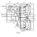
- the biopotential circuit 100 of an embodiment of the present invention comprises a pair of receive electrodes 101, 103 and a pair of drive electrodes 105, 107.
- the pair of receive electrodes 101, 103 is implanted into the patient's tissue.
- the drive electrodes 105, 107 are positioned either side of the receive electrodes to enclose an area 109 of the tissue.
- the drive electrodes may be positioned on the surface of the tissue as is known in the art.
- the biopotential circuit 100 further comprises a current generator 111 for generating the excitation current described in more detail below.
- the bio-potential circuit 100 further comprises an oscillator 113 and a demodulation clock 115.
- the oscillator 113 provides the reference clocks for the current generator 111 and the demodulation clock 115.
- the receive electrode outputs are fed to first and second analyzers 117, 119.
- Each analyzer 117, 119 is clocked by the demodulation clock 115.
- the second analyzer 119 compares the in phase component of the outputs of the pair of receive electrodes 101, 103 and the first analyzer 117 compares the quadrature phase components of the outputs of the pair of receive electrodes 101, 103 to determine the biopotential of the area 109 of the tissue.
- the respective components of the biopotential pass to respective first and second programmable gain amplifiers 121, 123, respective filters 125, 127 and buffers129, 131 to output the respective in phase component of the biopotential and the quadrature phase component of the bio-potential.
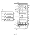
- the current generator 111 comprises a current digital-to-analog converter (DAC) 133 and a control module 135. As shown in more detail in Figure 2 .
- the control module 135 comprises a code generation module 201, a clock divider module 203 and a DAC selection module 205.
- the current DAC 133 comprises a first subset 207 of a plurality of parallel current cells 209_1 to 209_n.
- Each current cell 209_1 to 209_n of the first subset 207 comprises a pMOSFET 211_1 to 211_n.
- the pMOSFETs 211_1 to 211_n may be substantially similar, each generating the same amount of current.
- the source of each pMOSFET 211_1 to 211_n of the first subset 207 is connected in parallel to a common supply voltage V s .
- the gate of each pMOSFET 211_1 to 211_n of the first subset 207 is connected in common to a first bias voltage V biasp .
- each pMOSFET 211_1 to 211_n of the first subset 207 is connected to the respective source of a cascode pMOSFET 218_1 to 218_n of a first subset 217.
- the drain of each cascode pMOSFET 218_1 to 218_n of the first subset 217 is connected to a first terminal of a respective switch 213_1 to 213_n of a first subset 215.
- the second terminals of each switch 213_1 to 213_n of the first subset 215 are connected together to a first input of a combiner 219.
- the gate of each cascade pMOSFET 218_1 to 218_n of the first subset 217 is connected to a third bias V casp .
- the current cells 209_1 to 209_n of the first subset 207 provide a current source to generate positive alternations of a pseudo-sinusoidal alternating current.
- the current DAC 133 further comprises a second subset 221 of a plurality of parallel current cells 223_1 to 223_n.
- Each current cell 223_1 to 223_n of the second subset 221 comprises an nMOSFET 225_1 to 225_n.
- the nMOSFET 225_1 to 225_n may be substantially similar, each sinking the same amount of current.
- the source of each nMOSFET 225_1 to 225_n of the second subset 221 is connected in parallel to ground.
- the gate of each nMOSFET 225_1 to 225_n of the second subset 221 is connected in common to a second bias voltage V biasn .
- each nMOSFET 225_1 to 225_n of the second subset 221 is connected to the source of a respective cascode nMOSFET 232_1 to 232_n of a second subset 231.
- the drain of each cascode nMOSFET 232_1 to 232_n of the second subset 231 is connected to the first terminal of a respective switch 227_1 to 227_n of a second subset 221.
- the second terminal each switch 213_1 to 213_n of the first subset 215 are connected together to a second input of the combiner 219.
- the gate of each nMOSFET 232_1 to 232_n of the second subset 231 is connected to a fourth bias V casn .
- the current cells 223_1 to 223_n of the second subset 221 provide a current sink to generate the negative alternations of a pseudo- sinusoidal alternating current.
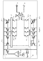
- the current DAC 133 is shown in more detail in Figure 3 .
- the first and second bias voltages V biasp , V biasn are provided via a current mirror pMOSFET 301.
- a reference current I REF is provided to the current mirror by a current reference circuit 305.
- the combiner 219 comprises a combination module 307 and a chopper 309. The chopper 309 outputs the generated components of the excitation current I 1 and the negative I 2 for drive electrodes 105, 107.
- the DAC selection module 205 comprises a first decoder 405.
- the output of the first decoder 405 provides the value to control the current generated by each current cell 209_1 to 209_n of the first subset 207 or sunk by each current cell 223_1 to 223_n of the second subset 221.
- each current cell comprises a plurality of MOSFETs connected in parallel (illustrated as a single variable MOSFET 411_1 and 423_1 in Figure 4 for simplicity), each of the parallel connected MOSFETs are turned on and off based on the control signal I AMP output by the first decoder 405.
- the input of the decoder 405 is connected to a third control signal AMPLITUDE.
- the code generation module 201 comprises a second decoder 439.
- the output of the second decoder 439 is connected to a multiplexer 441.
- the output of the multiplexer 441 is connected to a pseudo-sine synthesizer 443.
- the pseudo-sine synthesizer 443 is connected to a lookup table 445.
- the output of the pseudo-sine synthesizer 443 is connected to a wave selector 447.
- the output of the wave selector 447 is provided to control switching of the switches 213_1 to 213_n of the first subset 215 and the switches 227_1 to 227_n of the second subset 229.
- the pseudo-sine synthesizer 443 receives a first control signal SIGNAL_TYPE and the wave selector 447 receives a second control signal FREQUENCY.
- the clock divider module 203 also receives the second control signal FREQUENCY.
- the outputs of the clock divider 203 are connected to the second decoder 439 of the code generation module 201, the multiplexer 441 of the code generation module 201, the wave selector 447 of the code generation module 201 and the combiner 219.
- the clock divider 203 has a reference clock 437 connected to the clocking terminal of the clock divider 203. Operation of the current generator of Figures 2 to 5d will be described with reference to Figures 6 to 8 .
- the actuation of the switches is controlled by the control module 135.
- the switches are actuated according to a sequence.
- the coding for the switching sequence is stored in the lookup table 445 of the code generation module 201.
- the sequence is selected by the pseudo-sine synthesizer 443 from the coding stored in the lookup table 445 in response to the first control signal, SIGNAL_TYPE.
- the clock divider module 203 outputs the required modulation frequency selected by the second control signal, FREQUENCY.
- the wave selector 447 controls the switching frequency of each switch of the first and second subsets 215, 229 in accordance with the sequence provided by the pseudo-sine synthesizer 443.
- the DAC selection module 205 controls the amplitude of the modulation current output by the current generator in response to a third control signal AMPLITUDE by controlling the unit current for each current cell 209_1 to 209_n and 225_1 to 225_n.
- the unit current of the first subset and the second subset is substantially the same.
- an integer lookup table (LUT) with 64 values is designed which enables 16-level quantization.
- the third control signal AMPLITUDE is decoded by the first decoder 405 (in this specific example a 2 to 4 decoder) to generate a 4-bit I AMP ⁇ 0:3> signal.
- each current cell comprises four MOSFETs 411_1, 423_1 (for simplicity, the four MOSFETs are illustrated in the Figure as a single MOSFET) connected in parallel, each of the four MOSFETs are turned on and off based on the control signal I AMP ⁇ 0:3> output by the first decoder 405 to control the amplitude of the pseudo-sine waveform.
- the clock divider 203 generates a 4-bit IT ⁇ 0:3> signal. This is used to generate a 14 bit signal output by the multiplexer 441 which controls the pseudo-sine synthesizer 443 for accessing the LUT 445 with a SEL signal.
- SIGNAL_TYPE control signal selects the type of waveform for the output current, for example, a pseudo-sine-wave or square-wave.
- the 14 bit signals after Wave Selector are used as a switch control signals inside the unit current DACs.
- SIGNAL_TYPE Since the control signals, SIGNAL_TYPE, FREQUENCY and AMPLITUDE are independently provided to the current generator, a high programmable modulation current is generated.
- each switch of the first and second subset is therefore controlled in accordance with a sequence determined by the output of the DAC selection module 205.
- the output of each current cell 209_1 to 209_n of the first subset are summed, 603, by a first summer, formed in this embodiment, by the common connection of the switches.
- the output of the first summer is provided on the first input terminal of the combiner 219.
- each current cell 223_1 to 223_n of the second subset are summed, 607 by the second summer, formed in this embodiment, by the common connection of the switches 227_1 to 227_n of the second subset 229.
- the output of the second summer is provided on the second input terminal of the combiner 219.
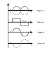
- the combined waveform is input to the chopper 309 which combines the waveform of Figure 5a with the square waveform of Figure 5b to output I 1 and I 2 as shown in Figure 5c and 5d .
- a 16-level quantized-sinusoidal current source is implemented which will suppress all harmonics power below the 63 rd harmonic.
- the switches of the DAC are switched in accordance with a code retrieved from the lookup table.
- An adaptively quantized integer LUT is used to reduce conversion error and reduce the requirements of a very high frequency clock as well as a high resolution DAC and this increasing power consumption.
- the integer LUT is achieved by the method shown in Figure 7 .
- Each non-integer coefficient for generating the pseudo-sinewave (shown in Figures 5c and 5d ) is received, 701, and converted into an integer, 703, for example, by rounding to the nearest integer.
- Adaptive quantisation, 705 is carried out on the converted integer so that the level of the quantisation is varied depending on the slop of the generated sine wave. As a result, when the slope is gentle, the quantisation is coarse with greater interval between changes in the quantisation level, for steeper slopes, the change in quantisation is lower at smaller change intervals.
- the adapted integer is the converted, 707 to Thermometer code and stored in the lookup for later retrieval.
- the ideal non-integer LUT and the integer LUT of the embodiment of the present invention lead to similar performance.
- demodulation can still be executed by a square wave using chopper demodulation while assuring 1% THD.
- the use of the PMOS and NMOS of the current cells of the DAC to generate the positive and negative alternations enables the NMOS sink matrix to reuse the current from the PMOS source matrix to maximize the power efficiency.
- the output chopper switch can mitigate the AC current mismatch between the current source and the current sink by alternating outputs at f CHOP frequency.
- scaling the size of each PMOS and NMOS can simply adjust the current magnitude (10-40 ⁇ A p-p ) to enable the high dynamic biopotential measurement range.
Landscapes
- Engineering & Computer Science (AREA)
- Theoretical Computer Science (AREA)
- Physics & Mathematics (AREA)
- General Engineering & Computer Science (AREA)
- General Physics & Mathematics (AREA)
- Power Engineering (AREA)
- Apparatus Associated With Microorganisms And Enzymes (AREA)
- Analogue/Digital Conversion (AREA)
Abstract
Description
- The invention relates to a current generator and a method of generating a current. In particular, but not exclusively, it relates to generating an excitation current for a biopotential measurement circuit.
- Bio-signal monitoring systems for monitoring a biological subject may involve measurement of the electrical potential differences in the tissue of the subject (biopotential). This is achieved by applying an excitation current across, in vivo, electrodes. Measurements are taken on a continuous basis. Therefore, the monitor is invariably implanted. Therefore, low power consumption whilst maintaining accuracy of the measurements is desirable.
- Therefore design strategies for each building block and signal monitoring methodology have to focus on low power consumption. In addition, measurement accuracy has to be guaranteed with minimized power consumption. There are two things which determine monitoring accuracy of portable bio-signal monitoring system. One is accuracy of the building block and the other is accuracy of monitoring method. To achieve high accuracy measurement requires high power consumption for internal building blocks and high accurate external components which increase form factor of the system.
- One specific bio-signal monitoring system is intra-thoracic fluid analysis. Such a measurement system is often required to resolve biopotential down to mΩ-range change (AC) superimposed on up to kΩ-range average (DC) impedance. In standard practice, this can be achieved by using a purely sinusoidal current source with very good harmonic distortion to minimize the error of impedance measurement as disclosed, for example, Yan, L.; Bae, J.; Lee, S.; Kim, B.; Roh. T.; Song, K.; Yoo, H-J.;, "A 3.9mW 25-electrode Reconfigurable Thoracic Impedance/ECG SoC with Body-Channel Transponder," IEEE International Solid-State Circuits Conference, vol., no., pp.490-491, 7-11 Feb. 2010. However, this approach consumes many mWs of power which is not acceptable for an implantable device. There is research that uses multi-level quantized signal as a modulation and demodulation signal as disclosed in M. Min, and T. Parve, "Improvement of Lock-in Electrical Bio-Impedance Analyzer for Implantable Medical Devices," IEEE Tran. On Instrumentation and Measurement, 2007. As a result, µW-range power consumption can be achieved by using a square-wave current combined with quadrature demodulation as disclosed, for example, in Yazicioglu, R.F.; Kim, S.; Torfs, T.; Merken, P.; Van Hoof, C.; , "A 30µW Analog Signal Processor ASIC for biomedical signal monitoring," IEEE International Solid-State Circuits Conference, vol., no., pp.124-125, 7-11 Feb. 2010. This technique, however, requires multi-level quantized current as well as multi-level demodulation amplifier which has a complex architecture and consumes more power. In addition, this technique requires modulation and demodulation signal which have accurately generated phase shift. This limits programmability of the generated signal as well as the measurement accuracy can be degraded due to the phase variations. Further, resulting in intolerable measurement errors as high as 23% because the quadrature demodulation will fold all odd harmonics of the square wave current into the baseband.
- The present invention aims to provide a current generator that would be suitable for use in an implantable biopotential monitoring system which mitigates the above mentioned drawbacks.
- There is therefore provided a current generator comprising a plurality of current cells connected in parallel, each current cell being connected to a switch; a summer configured to sum the output of each current cell; wherein each switch is switchable according to a sequence to generate a summed output of the current cells at a plurality of quantisation levels to generate positive and/or negative alternations of a pseudo-sinusoidal, alternating current.
- According to another aspect of the invention, there is provided a biopotential measurement system comprising a current generator above.
- According to yet another aspect of the invention, there is provided a method for generating a current, the method comprising the steps of switching a plurality of current cells, each current cell being connected in parallel; summing the output of each current cell of a first subset of the plurality of current cells for generating positive alternations of the pseudo-sinusoidal, alternating current; summing the output of each current cell of a second subset of the plurality of current cells for generating negative alternations of the pseudo-sinusoidal, alternating current; combining the summations of the output of each current cell of the first subset of the plurality of current cells and the output of each current cell of the second subset of the plurality of current cells to generate a pseudo-sinusoidal alternating current; and wherein switching the plurality of current cells comprises switching each current cell according to a sequence to generate a summed output of the current cells at a plurality of quantisation levels to generate positive and/or negative alternations of a pseudo-sinusoidal, alternating current.
- To achieve a high accurate biopotential monitoring system with low power consumption, a multi-mode current injection circuit is used to generate the current. A pseudo-sine wave current is generated via internal digital control circuit which is particularly useful for monitoring biopotential as well as conventional square wave excitation current.
- Each current cell of the first subset of the plurality of current cells may comprise a current source. Each switch of the current cells of the first subset of the plurality of current cells may be switched according to the sequence to generate a summed output of the current cells of the first subset at a plurality of quantisation levels to generate the positive alternations of the pseudo-sinusoidal, alternating current.
- Each current cell of the second subset of the plurality of current cells may comprise a current sink. Each switch of the current cells of the second subset of the plurality of current cells may be switched according to the sequence to generate a summed output of the current cells of the second subset at a plurality of quantisation levels to generate the negative alternations of the pseudo-sinusoidal, alternating current.
- In an embodiment, the combiner further comprises a chopper configured to chop alternating alternations of the outputs of the first and second summers to generating alternate positive and negative alternations of a pseudo-sinusoidal, alternating current.
- In a further embodiment, the current generator further comprises a control module configured to provide the sequence to generate the summed output of the current cells and to adjust the number of quantisation levels.
- The control module further may comprise a look up table configured to store the coding for the sequence. The look up table may comprise an integer look-up table.
- In yet a further embedment, the control module is configured to adapt the sequence in order to change the frequency and amplitude of the generated pseudo-sinusoidal, alternating current. The control module is configured to change the switchable frequency of each switch and the combination frequency of the combiner. The control module is configured to increase or decrease the unit current of each current cell to increase or decrease the amplitude of the pseudo-sinusoidal alternating current.
- The invention will now be described, by way of example only, with reference to the following drawings, in which:
-
Figure 1 is a simplified schematic of an example of a bio-impedance measuring circuit including the current generator of an embodiment of the present invention; -
Figure 2 is a simplified schematic of the current generator according to an embodiment of the present invention; -
Figure 3 is a simplified schematic of the current digital-to-analog converter of the current generator ofFigure 2 ; -
Figure 4 is a simplified schematic of the current generator of another embodiment according to the present invention; -
Figure 5a is a graphical representation of the output of the combiner of the embodiment of the present invention; -
Figure 5b is a graphical representation of the chopper waveform of the chopper of the embodiment of the present invention; -
Figure 5c is a graphical representation of one component I1, of the generated current of the current generator of the embodiment of the present invention; -
Figure 5d is a graphical representation of the second component I2 of the generated current of the current generator of the embodiment of the present invention; -
Figure 6 is a flowchart of the method of generating a current according to an embodiment of the present invention; -
Figure 7 is a flowchart of the method of generating the integer coefficient for the look up table of the controller of the current generator according to an embodiment of the present invention; and -
Figure 8 is a graphical representation of a comparison of the waveforms generated by a non-integer look up table and the integer lookup table according to an embodiment of the present invention. - With reference to
Figure 1 , thebiopotential circuit 100 of an embodiment of the present invention comprises a pair of receiveelectrodes drive electrodes electrodes drive electrodes area 109 of the tissue. The drive electrodes may be positioned on the surface of the tissue as is known in the art. - An excitation current is applied to the
drive electrodes area 109 of the tissue is measured by the receiveelectrode pair biopotential circuit 100 further comprises acurrent generator 111 for generating the excitation current described in more detail below. Thebio-potential circuit 100 further comprises anoscillator 113 and ademodulation clock 115. Theoscillator 113 provides the reference clocks for thecurrent generator 111 and thedemodulation clock 115. - The receive electrode outputs are fed to first and
second analyzers analyzer demodulation clock 115. Thesecond analyzer 119 compares the in phase component of the outputs of the pair of receiveelectrodes first analyzer 117 compares the quadrature phase components of the outputs of the pair of receiveelectrodes area 109 of the tissue. The respective components of the biopotential pass to respective first and secondprogrammable gain amplifiers respective filters - The
current generator 111 comprises a current digital-to-analog converter (DAC) 133 and acontrol module 135. As shown in more detail inFigure 2 . Thecontrol module 135 comprises acode generation module 201, aclock divider module 203 and aDAC selection module 205. - The
current DAC 133 comprises afirst subset 207 of a plurality of parallel current cells 209_1 to 209_n. Each current cell 209_1 to 209_n of thefirst subset 207 comprises a pMOSFET 211_1 to 211_n. The pMOSFETs 211_1 to 211_n may be substantially similar, each generating the same amount of current. The source of each pMOSFET 211_1 to 211_n of thefirst subset 207 is connected in parallel to a common supply voltage Vs. The gate of each pMOSFET 211_1 to 211_n of thefirst subset 207 is connected in common to a first bias voltage Vbiasp. The drain of each pMOSFET 211_1 to 211_n of thefirst subset 207 is connected to the respective source of a cascode pMOSFET 218_1 to 218_n of afirst subset 217. The drain of each cascode pMOSFET 218_1 to 218_n of thefirst subset 217 is connected to a first terminal of a respective switch 213_1 to 213_n of afirst subset 215. The second terminals of each switch 213_1 to 213_n of thefirst subset 215 are connected together to a first input of acombiner 219. The gate of each cascade pMOSFET 218_1 to 218_n of thefirst subset 217 is connected to a third bias Vcasp. The current cells 209_1 to 209_n of thefirst subset 207 provide a current source to generate positive alternations of a pseudo-sinusoidal alternating current. - The
current DAC 133 further comprises asecond subset 221 of a plurality of parallel current cells 223_1 to 223_n. Each current cell 223_1 to 223_n of thesecond subset 221 comprises an nMOSFET 225_1 to 225_n. The nMOSFET 225_1 to 225_n may be substantially similar, each sinking the same amount of current. The source of each nMOSFET 225_1 to 225_n of thesecond subset 221 is connected in parallel to ground. The gate of each nMOSFET 225_1 to 225_n of thesecond subset 221 is connected in common to a second bias voltage Vbiasn. The drain of each nMOSFET 225_1 to 225_n of thesecond subset 221 is connected to the source of a respective cascode nMOSFET 232_1 to 232_n of asecond subset 231. The drain of each cascode nMOSFET 232_1 to 232_n of thesecond subset 231 is connected to the first terminal of a respective switch 227_1 to 227_n of asecond subset 221. The second terminal each switch 213_1 to 213_n of thefirst subset 215 are connected together to a second input of thecombiner 219. The gate of each nMOSFET 232_1 to 232_n of thesecond subset 231 is connected to a fourth bias Vcasn. The current cells 223_1 to 223_n of thesecond subset 221 provide a current sink to generate the negative alternations of a pseudo- sinusoidal alternating current. - The
current DAC 133 is shown in more detail inFigure 3 . The first and second bias voltages Vbiasp, Vbiasn are provided via acurrent mirror pMOSFET 301. A reference current IREF is provided to the current mirror by acurrent reference circuit 305. Thecombiner 219 comprises acombination module 307 and achopper 309. Thechopper 309 outputs the generated components of the excitation current I1 and the negative I2 fordrive electrodes - In an embodiment as shown in
Figure 4 , theDAC selection module 205 comprises afirst decoder 405. The output of thefirst decoder 405 provides the value to control the current generated by each current cell 209_1 to 209_n of thefirst subset 207 or sunk by each current cell 223_1 to 223_n of thesecond subset 221. In this embodiment each current cell comprises a plurality of MOSFETs connected in parallel (illustrated as a single variable MOSFET 411_1 and 423_1 inFigure 4 for simplicity), each of the parallel connected MOSFETs are turned on and off based on the control signal IAMP output by the first decoder 405.The input of thedecoder 405 is connected to a third control signal AMPLITUDE. Thecode generation module 201 comprises asecond decoder 439. The output of thesecond decoder 439 is connected to amultiplexer 441. The output of themultiplexer 441 is connected to apseudo-sine synthesizer 443. Thepseudo-sine synthesizer 443 is connected to a lookup table 445. The output of thepseudo-sine synthesizer 443 is connected to awave selector 447. The output of thewave selector 447 is provided to control switching of the switches 213_1 to 213_n of thefirst subset 215 and the switches 227_1 to 227_n of thesecond subset 229. Thepseudo-sine synthesizer 443 receives a first control signal SIGNAL_TYPE and thewave selector 447 receives a second control signal FREQUENCY. Theclock divider module 203 also receives the second control signal FREQUENCY. The outputs of theclock divider 203 are connected to thesecond decoder 439 of thecode generation module 201, themultiplexer 441 of thecode generation module 201, thewave selector 447 of thecode generation module 201 and thecombiner 219. Theclock divider 203 has areference clock 437 connected to the clocking terminal of theclock divider 203. Operation of the current generator ofFigures 2 to 5d will be described with reference toFigures 6 to 8 . - The actuation of the switches is controlled by the
control module 135. The switches are actuated according to a sequence. The coding for the switching sequence is stored in the lookup table 445 of thecode generation module 201. The sequence is selected by thepseudo-sine synthesizer 443 from the coding stored in the lookup table 445 in response to the first control signal, SIGNAL_TYPE. Theclock divider module 203 outputs the required modulation frequency selected by the second control signal, FREQUENCY. Thewave selector 447 controls the switching frequency of each switch of the first andsecond subsets pseudo-sine synthesizer 443. TheDAC selection module 205 controls the amplitude of the modulation current output by the current generator in response to a third control signal AMPLITUDE by controlling the unit current for each current cell 209_1 to 209_n and 225_1 to 225_n. The unit current of the first subset and the second subset is substantially the same. In an example, to generate pseudo-sinewave, an integer lookup table (LUT) with 64 values is designed which enables 16-level quantization. The third control signal AMPLITUDE is decoded by the first decoder 405 (in this specific example a 2 to 4 decoder) to generate a 4-bit IAMP<0:3> signal. In this example, each current cell comprises four MOSFETs 411_1, 423_1 (for simplicity, the four MOSFETs are illustrated in the Figure as a single MOSFET) connected in parallel, each of the four MOSFETs are turned on and off based on the control signal IAMP<0:3> output by thefirst decoder 405 to control the amplitude of the pseudo-sine waveform. Theclock divider 203 generates a 4-bit IT<0:3> signal. This is used to generate a 14 bit signal output by themultiplexer 441 which controls thepseudo-sine synthesizer 443 for accessing theLUT 445 with a SEL signal. SIGNAL_TYPE control signal selects the type of waveform for the output current, for example, a pseudo-sine-wave or square-wave. The 14 bit signals after Wave Selector are used as a switch control signals inside the unit current DACs. - Since the control signals, SIGNAL_TYPE, FREQUENCY and AMPLITUDE are independently provided to the current generator, a high programmable modulation current is generated.
- The switching 601, 605 of each switch of the first and second subset is therefore controlled in accordance with a sequence determined by the output of the
DAC selection module 205. The output of each current cell 209_1 to 209_n of the first subset are summed, 603, by a first summer, formed in this embodiment, by the common connection of the switches. The output of the first summer is provided on the first input terminal of thecombiner 219. - The output of each current cell 223_1 to 223_n of the second subset are summed, 607 by the second summer, formed in this embodiment, by the common connection of the switches 227_1 to 227_n of the
second subset 229. The output of the second summer is provided on the second input terminal of thecombiner 219. - The summation M*IREF+ΔIp (wherein M is the number of current cells of the first subset connected at any one time, ΔIp is the error of the summed output of the current cells of the first subset 207due to mismatch) and the summation -M*IREF-ΔIn (wherein M is the number of current cells of the second subset connected at any one time, ΔIn is the error of the summed output of the current cells of the
second subset 221 due to mismatch) are combined, 609, to form the combined waveform as shown inFigure 5a . The combined waveform is input to thechopper 309 which combines the waveform ofFigure 5a with the square waveform ofFigure 5b to output I1 and I2 as shown inFigure 5c and 5d . The alternate alternations are then chopped, 611 to form a pseudo-sinusoidal alternating current I1 =2M*IREF+Δ(Ip+In) and the negative I2=-{2M*IREF+Δ(Ip+In)}. - To limit the Total Harmonic Distortion (THD) due to folded odd harmonics to less than 1%, a 16-level quantized-sinusoidal current source is implemented which will suppress all harmonics power below the 63rd harmonic. In order to generate such a quantized current source with ideal sinewave characteristics, the switches of the DAC are switched in accordance with a code retrieved from the lookup table. An adaptively quantized integer LUT is used to reduce conversion error and reduce the requirements of a very high frequency clock as well as a high resolution DAC and this increasing power consumption. By assigning different number of currents cells based on the amplitude of the resulting modulation signal, conversion errors decease by 1.71-fold. Using current cells minimizes the mismatch of the current generator and prevents glitches due to simultaneous switching of the DAC as well as enables easy configuration of the injection current amplitude. The integer LUT is achieved by the method shown in
Figure 7 . Each non-integer coefficient for generating the pseudo-sinewave (shown inFigures 5c and 5d ) is received, 701, and converted into an integer, 703, for example, by rounding to the nearest integer. Adaptive quantisation, 705 is carried out on the converted integer so that the level of the quantisation is varied depending on the slop of the generated sine wave. As a result, when the slope is gentle, the quantisation is coarse with greater interval between changes in the quantisation level, for steeper slopes, the change in quantisation is lower at smaller change intervals. The adapted integer is the converted, 707 to Thermometer code and stored in the lookup for later retrieval. As illustrated inFigure 8 , the ideal non-integer LUT and the integer LUT of the embodiment of the present invention lead to similar performance. As a result, demodulation can still be executed by a square wave using chopper demodulation while assuring 1% THD. - By adopting a pseudo-sine wave current generator with low power current DAC architecture, high resolution bio-impedance monitoring is enabled as well as low power monitoring by adopting a square wave current generator.
- The use of the PMOS and NMOS of the current cells of the DAC to generate the positive and negative alternations enables the NMOS sink matrix to reuse the current from the PMOS source matrix to maximize the power efficiency. Further, the output chopper switch can mitigate the AC current mismatch between the current source and the current sink by alternating outputs at fCHOP frequency. Furthermore, scaling the size of each PMOS and NMOS can simply adjust the current magnitude (10-40µAp-p) to enable the high dynamic biopotential measurement range.
- Although embodiments of the present invention have been illustrated in the accompanying drawings and described in the foregoing detailed description, it will be understood that the invention is not limited to the embodiments disclosed, but capable of numerous modifications without departing from the scope of the invention as set out in the following claims. In the claims, the word "comprising" does not exclude other elements or steps, and the indefinite article "a" or "an" does not exclude a plurality. Any reference signs in the claims should not be construed as limiting the scope.
Claims (13)
- A current generator comprising:a plurality of current cells connected in parallel, each current cell being connected to a switch;a first summer configured to sum the output of each current cell of a first subset of the plurality of current cells and a second summer configured to sum the output of each current cell of a second subset of the plurality of current cells;a combiner configured to combine the outputs of the first and second summers; andwherein each switch is switchable according to a sequence to generate a summed output of the current cells at a plurality of quantisation levels to generate positive and/or negative alternations of a pseudo-sinusoidal, alternating current.
- A current generator according to claim 1, wherein each current cell of the first subset of the plurality of current cells comprises a current source and wherein each switch of the current cells of the first subset of the plurality of current cells is switched according to the sequence to generate a summed output of the current cells of the first subset at a plurality of quantisation levels to generate the positive alternations of the pseudo-sinusoidal, alternating current.
- A current source according to any one of the preceding claims, wherein each current cell of the second subset of the plurality of current cells comprises a current sink and wherein each switch of the current cells of the second subset of the plurality of current cells is switched according to the sequence to generate a summed output of the current cells of the second subset at a plurality of quantisation levels to generate the negative alternations of the pseudo-sinusoidal, alternating current.
- A current generator according to any one of the preceding claims, wherein the combiner further comprises a chopper configured to chop alternating alternations of the outputs of the first and second summers to generating alternate positive and negative alternations of a pseudo-sinusoidal, alternating current.
- A current generator according to any one of the preceding claims, wherein the current generator further comprises a control module configured to provide the sequence to generate the summed output of the current cells and to adjust the number of quantisation levels.
- A current generator according to claim 5, wherein the control module further comprises a look up table configured to store the coding for the sequence.
- A current generator according to claim 6, wherein the look up table comprises an integer look-up table.
- A current generator according to any one of claims 5 to 7, wherein the control module is further configured to adapt the sequence in order to change the frequency and/or amplitude of the generated pseudo-sinusoidal, alternating current.
- A current generator according to claim 8 wherein the control module is configured to change the switchable frequency of each switch and the combination frequency of the combiner.
- A current generator according to any one of claims 8 or 9 wherein the control module is configured to increase or decrease the unit current of each current cell to increase or decrease the amplitude of the pseudo-sinusoidal alternating current.
- A biopotential measurement system comprising a current generator according to any one of the preceding claims.
- A method for generating a current, the method comprising the steps of:switching a plurality of current cells, each current cell being connected in parallel;summing the output of each current cell of a first subset of the plurality of current cells for generating positive alternations of the pseudo-sinusoidal, alternating current;summing the output of each current cell of a second subset of the plurality of current cells for generating negative alternations of the pseudo-sinusoidal, alternating current;combining the summations of the output of each current cell of the first subset of the plurality of current cells and the output of each current cell of the second subset of the plurality of current cells to generate a pseudo-sinusoidal alternating current; andwherein switching the plurality of current cells comprises switching each current cell according to a sequence to generate a summed output of the current cells at a plurality of quantisation levels to generate positive and/or negative alternations of a pseudo-sinusoidal, alternating current.
- A method according to claim 12, wherein the method further comprises the step of:chopping alternating alternations of the combined alternations to generating alternate positive and negative alternations of the pseudo sinusoidal alternating current.
Priority Applications (2)
| Application Number | Priority Date | Filing Date | Title |
|---|---|---|---|
| EP12198406.6A EP2746891B1 (en) | 2012-12-20 | 2012-12-20 | A current waveform generator |
| US14/107,399 US9391456B2 (en) | 2012-12-20 | 2013-12-16 | Current generator |
Applications Claiming Priority (1)
| Application Number | Priority Date | Filing Date | Title |
|---|---|---|---|
| EP12198406.6A EP2746891B1 (en) | 2012-12-20 | 2012-12-20 | A current waveform generator |
Publications (2)
| Publication Number | Publication Date |
|---|---|
| EP2746891A1 true EP2746891A1 (en) | 2014-06-25 |
| EP2746891B1 EP2746891B1 (en) | 2015-06-03 |
Family
ID=47678494
Family Applications (1)
| Application Number | Title | Priority Date | Filing Date |
|---|---|---|---|
| EP12198406.6A Active EP2746891B1 (en) | 2012-12-20 | 2012-12-20 | A current waveform generator |
Country Status (2)
| Country | Link |
|---|---|
| US (1) | US9391456B2 (en) |
| EP (1) | EP2746891B1 (en) |
Cited By (1)
| Publication number | Priority date | Publication date | Assignee | Title |
|---|---|---|---|---|
| EP3009911A1 (en) * | 2014-10-14 | 2016-04-20 | Conti Temic microelectronic GmbH | Signal generating device and integrated circuit |
Families Citing this family (1)
| Publication number | Priority date | Publication date | Assignee | Title |
|---|---|---|---|---|
| WO2016015224A1 (en) * | 2014-07-29 | 2016-02-04 | 华为技术有限公司 | Receiver and signal processing method |
Citations (2)
| Publication number | Priority date | Publication date | Assignee | Title |
|---|---|---|---|---|
| EP1035646A1 (en) * | 1999-03-05 | 2000-09-13 | Infineon Technologies AG | Circuit for a controllable amplifier |
| US20120049904A1 (en) * | 2010-08-24 | 2012-03-01 | Franz Kuttner | Digital Waveform Synthesis |
Family Cites Families (16)
| Publication number | Priority date | Publication date | Assignee | Title |
|---|---|---|---|---|
| JPH0595287A (en) * | 1991-10-01 | 1993-04-16 | Mitsubishi Electric Corp | Subtraction circuit and A / D converter including the subtraction circuit |
| JP3528958B2 (en) * | 2000-06-28 | 2004-05-24 | 松下電器産業株式会社 | Current addition type DA converter |
| US6831581B1 (en) * | 2003-05-23 | 2004-12-14 | Infineon Technologies, Ag | Digital-to-analog converter arrangement with an array of unary digital-to-analog converting elements usable for different signal types |
| US20050038846A1 (en) * | 2003-08-14 | 2005-02-17 | Devendorf Don C. | Substraction circuit with a dummy digital to analog converter |
| US6950047B1 (en) * | 2004-03-31 | 2005-09-27 | Silicon Labs Cp, Inc. | Method and apparatus for combining outputs of multiple DACs for increased bit resolution |
| JP4155406B2 (en) * | 2004-04-01 | 2008-09-24 | ソニー・エリクソン・モバイルコミュニケーションズ株式会社 | Delta-sigma modulation type fractional frequency division PLL frequency synthesizer and radio communication apparatus |
| US7466252B1 (en) * | 2007-07-12 | 2008-12-16 | Xilinx, Inc. | Method and apparatus for calibrating a scaled current electronic circuit |
| US8094055B2 (en) * | 2010-01-26 | 2012-01-10 | Power Integrations, Inc. | Compact digital-to-analog converter |
| US8018365B1 (en) * | 2010-03-14 | 2011-09-13 | Mediatek Inc. | Continuous-time delta-sigma ADC with compact structure |
| US8344922B2 (en) * | 2010-08-03 | 2013-01-01 | Crest Semiconductors, Inc. | Digital-to-analog converter with code independent output capacitance |
| US8760331B2 (en) * | 2012-01-20 | 2014-06-24 | Hittite Microwave Norway As | Continuous time delta sigma converter having a VCO based quantizer |
| US8847807B2 (en) * | 2012-11-26 | 2014-09-30 | Analog Devices, Inc. | Switching scheme for ISI mitigation in data converters |
| CN104298287B (en) * | 2013-07-17 | 2016-04-20 | 联发科技(新加坡)私人有限公司 | Current correction method and device and resistance bearing calibration and device |
| US9094042B2 (en) * | 2013-08-09 | 2015-07-28 | Silicon Laboratories Inc. | DAC current source matrix patterns with gradient error cancellation |
| US9065477B2 (en) * | 2013-09-03 | 2015-06-23 | Analog Devices Global | Linear and DC-accurate frontend DAC and input structure |
| US9136854B1 (en) * | 2014-06-30 | 2015-09-15 | Cadence Design Systems, Inc. | Current switching digital-to-analog converter with hybrid current switching circuit having low-memory effect |
-
2012
- 2012-12-20 EP EP12198406.6A patent/EP2746891B1/en active Active
-
2013
- 2013-12-16 US US14/107,399 patent/US9391456B2/en active Active
Patent Citations (2)
| Publication number | Priority date | Publication date | Assignee | Title |
|---|---|---|---|---|
| EP1035646A1 (en) * | 1999-03-05 | 2000-09-13 | Infineon Technologies AG | Circuit for a controllable amplifier |
| US20120049904A1 (en) * | 2010-08-24 | 2012-03-01 | Franz Kuttner | Digital Waveform Synthesis |
Non-Patent Citations (2)
| Title |
|---|
| YAN, L.; BAE, J.; LEE, S.; KIM, B.; ROH. T.; SONG, K.; YOO, H-J.: "A 3.9mW 25-electrode Reconfigurable Thoracic Impedance/ECG SoC with Body-Channel Transponder", IEEE INTERNATIONAL SOLID-STATE CIRCUITS CONFERENCE, 7 February 2010 (2010-02-07), pages 490 - 491, XP031649925 |
| YAZICIOGLU, R.F.; KIM, S.; TORFS, T.; MERKEN, P.; VAN HOOF, C.: "A 30pW Analog Signal Processor ASIC for biomedical signal monitoring", IEEE INTERNATIONAL SOLID-STATE CIRCUITS CONFERENCE, 7 February 2010 (2010-02-07), pages 124 - 125, XP031650111 |
Cited By (1)
| Publication number | Priority date | Publication date | Assignee | Title |
|---|---|---|---|---|
| EP3009911A1 (en) * | 2014-10-14 | 2016-04-20 | Conti Temic microelectronic GmbH | Signal generating device and integrated circuit |
Also Published As
| Publication number | Publication date |
|---|---|
| US9391456B2 (en) | 2016-07-12 |
| US20140175891A1 (en) | 2014-06-26 |
| EP2746891B1 (en) | 2015-06-03 |
Similar Documents
| Publication | Publication Date | Title |
|---|---|---|
| US9444323B2 (en) | Power conversion system having a harmonic distortion limiter | |
| CN111896800B (en) | Power measurement device and method based on pulse-driven alternating-current quantum voltage source | |
| WO2004100344A3 (en) | Method and apparatus for tracking maximum power point for inverters in photovoltaic applications | |
| Elserougi et al. | Conceptual study of a bipolar modular high voltage pulse generator with sequential charging | |
| US8970063B2 (en) | Method and arrangement for balancing voltages of series connection of storage units for electrical energy | |
| EP2746891B1 (en) | A current waveform generator | |
| CN111900956A (en) | Power generation device based on pulse driving type alternating current quantum voltage source | |
| TW201134078A (en) | Power supply device having an adjustable switching frequency | |
| JP6158125B2 (en) | Power converter | |
| Babu | Comparative analysis of cascadeded multilevel inverter for phase disposition and phase shift carrier PWM for different load | |
| US8791849B1 (en) | Digital clock update methodology for multi-Nyquist constructive interference to boost signal power in radio frequency transmission | |
| Palanivel et al. | Multicarrier pulse width modulation methods based three phase cascaded multilevel inverter including over modulation and low modulation indices | |
| US8901998B2 (en) | Current-voltage converter having a current reflector, input stage of an amplifier and corresponding amplifier | |
| Ojarand et al. | Efficient excitation signals for the fast impedance spectroscopy | |
| Faktorová et al. | Implementation of the impedance spectroscopy using a modern microcontroller | |
| GB2627351A (en) | Electrochemical cell characterisation | |
| Palanivel et al. | Phase shifted carrier pulse width modulation for three phase multilevel inverter to minimize THD and enhance output voltage performance | |
| Lopatkin | Voltage THD and integrated voltage harmonics factors of three-phase multilevel voltage source inverter with nearest vector selecting space vector control | |
| US20150016168A1 (en) | Highly stable maximum power point tracking for bipolar photovoltaic inverters | |
| US8896331B2 (en) | Impedance measuring instrument | |
| US12287658B2 (en) | Power supplies and improved signal adjustment | |
| US9112527B2 (en) | Digital-to-analog sinusoidal driver apparatus, systems and methods | |
| Palanivel et al. | Comparative study of constant switching frequency and variable switching frequency multicarrier pulse width modulation for three phase cascaded multilevel inverter | |
| Rajavel et al. | A new configuration of multilevel inverter to generate higher voltage level with lower components | |
| RU2713389C2 (en) | Multi-zone dc/ac converter |
Legal Events
| Date | Code | Title | Description |
|---|---|---|---|
| PUAI | Public reference made under article 153(3) epc to a published international application that has entered the european phase |
Free format text: ORIGINAL CODE: 0009012 |
|
| 17P | Request for examination filed |
Effective date: 20121220 |
|
| AK | Designated contracting states |
Kind code of ref document: A1 Designated state(s): AL AT BE BG CH CY CZ DE DK EE ES FI FR GB GR HR HU IE IS IT LI LT LU LV MC MK MT NL NO PL PT RO RS SE SI SK SM TR |
|
| AX | Request for extension of the european patent |
Extension state: BA ME |
|
| R17P | Request for examination filed (corrected) |
Effective date: 20141125 |
|
| RBV | Designated contracting states (corrected) |
Designated state(s): AL AT BE BG CH CY CZ DE DK EE ES FI FR GB GR HR HU IE IS IT LI LT LU LV MC MK MT NL NO PL PT RO RS SE SI SK SM TR |
|
| GRAP | Despatch of communication of intention to grant a patent |
Free format text: ORIGINAL CODE: EPIDOSNIGR1 |
|
| RIC1 | Information provided on ipc code assigned before grant |
Ipc: G06F 1/03 20060101ALI20141219BHEP Ipc: G06F 1/02 20060101AFI20141219BHEP |
|
| INTG | Intention to grant announced |
Effective date: 20150121 |
|
| GRAS | Grant fee paid |
Free format text: ORIGINAL CODE: EPIDOSNIGR3 |
|
| GRAA | (expected) grant |
Free format text: ORIGINAL CODE: 0009210 |
|
| AK | Designated contracting states |
Kind code of ref document: B1 Designated state(s): AL AT BE BG CH CY CZ DE DK EE ES FI FR GB GR HR HU IE IS IT LI LT LU LV MC MK MT NL NO PL PT RO RS SE SI SK SM TR |
|
| REG | Reference to a national code |
Ref country code: GB Ref legal event code: FG4D |
|
| REG | Reference to a national code |
Ref country code: CH Ref legal event code: EP |
|
| REG | Reference to a national code |
Ref country code: AT Ref legal event code: REF Ref document number: 730227 Country of ref document: AT Kind code of ref document: T Effective date: 20150715 Ref country code: IE Ref legal event code: FG4D |
|
| REG | Reference to a national code |
Ref country code: DE Ref legal event code: R096 Ref document number: 602012007718 Country of ref document: DE Effective date: 20150716 |
|
| REG | Reference to a national code |
Ref country code: AT Ref legal event code: MK05 Ref document number: 730227 Country of ref document: AT Kind code of ref document: T Effective date: 20150603 |
|
| PG25 | Lapsed in a contracting state [announced via postgrant information from national office to epo] |
Ref country code: FI Free format text: LAPSE BECAUSE OF FAILURE TO SUBMIT A TRANSLATION OF THE DESCRIPTION OR TO PAY THE FEE WITHIN THE PRESCRIBED TIME-LIMIT Effective date: 20150603 Ref country code: LT Free format text: LAPSE BECAUSE OF FAILURE TO SUBMIT A TRANSLATION OF THE DESCRIPTION OR TO PAY THE FEE WITHIN THE PRESCRIBED TIME-LIMIT Effective date: 20150603 Ref country code: HR Free format text: LAPSE BECAUSE OF FAILURE TO SUBMIT A TRANSLATION OF THE DESCRIPTION OR TO PAY THE FEE WITHIN THE PRESCRIBED TIME-LIMIT Effective date: 20150603 Ref country code: NO Free format text: LAPSE BECAUSE OF FAILURE TO SUBMIT A TRANSLATION OF THE DESCRIPTION OR TO PAY THE FEE WITHIN THE PRESCRIBED TIME-LIMIT Effective date: 20150903 Ref country code: ES Free format text: LAPSE BECAUSE OF FAILURE TO SUBMIT A TRANSLATION OF THE DESCRIPTION OR TO PAY THE FEE WITHIN THE PRESCRIBED TIME-LIMIT Effective date: 20150603 |
|
| REG | Reference to a national code |
Ref country code: NL Ref legal event code: MP Effective date: 20150603 |
|
| REG | Reference to a national code |
Ref country code: FR Ref legal event code: PLFP Year of fee payment: 4 |
|
| REG | Reference to a national code |
Ref country code: LT Ref legal event code: MG4D |
|
| PG25 | Lapsed in a contracting state [announced via postgrant information from national office to epo] |
Ref country code: RS Free format text: LAPSE BECAUSE OF FAILURE TO SUBMIT A TRANSLATION OF THE DESCRIPTION OR TO PAY THE FEE WITHIN THE PRESCRIBED TIME-LIMIT Effective date: 20150603 Ref country code: AT Free format text: LAPSE BECAUSE OF FAILURE TO SUBMIT A TRANSLATION OF THE DESCRIPTION OR TO PAY THE FEE WITHIN THE PRESCRIBED TIME-LIMIT Effective date: 20150603 Ref country code: LV Free format text: LAPSE BECAUSE OF FAILURE TO SUBMIT A TRANSLATION OF THE DESCRIPTION OR TO PAY THE FEE WITHIN THE PRESCRIBED TIME-LIMIT Effective date: 20150603 Ref country code: BG Free format text: LAPSE BECAUSE OF FAILURE TO SUBMIT A TRANSLATION OF THE DESCRIPTION OR TO PAY THE FEE WITHIN THE PRESCRIBED TIME-LIMIT Effective date: 20150903 Ref country code: GR Free format text: LAPSE BECAUSE OF FAILURE TO SUBMIT A TRANSLATION OF THE DESCRIPTION OR TO PAY THE FEE WITHIN THE PRESCRIBED TIME-LIMIT Effective date: 20150904 |
|
| PG25 | Lapsed in a contracting state [announced via postgrant information from national office to epo] |
Ref country code: EE Free format text: LAPSE BECAUSE OF FAILURE TO SUBMIT A TRANSLATION OF THE DESCRIPTION OR TO PAY THE FEE WITHIN THE PRESCRIBED TIME-LIMIT Effective date: 20150603 |
|
| PG25 | Lapsed in a contracting state [announced via postgrant information from national office to epo] |
Ref country code: PT Free format text: LAPSE BECAUSE OF FAILURE TO SUBMIT A TRANSLATION OF THE DESCRIPTION OR TO PAY THE FEE WITHIN THE PRESCRIBED TIME-LIMIT Effective date: 20151006 Ref country code: IS Free format text: LAPSE BECAUSE OF FAILURE TO SUBMIT A TRANSLATION OF THE DESCRIPTION OR TO PAY THE FEE WITHIN THE PRESCRIBED TIME-LIMIT Effective date: 20151003 Ref country code: CZ Free format text: LAPSE BECAUSE OF FAILURE TO SUBMIT A TRANSLATION OF THE DESCRIPTION OR TO PAY THE FEE WITHIN THE PRESCRIBED TIME-LIMIT Effective date: 20150603 Ref country code: SK Free format text: LAPSE BECAUSE OF FAILURE TO SUBMIT A TRANSLATION OF THE DESCRIPTION OR TO PAY THE FEE WITHIN THE PRESCRIBED TIME-LIMIT Effective date: 20150603 Ref country code: PL Free format text: LAPSE BECAUSE OF FAILURE TO SUBMIT A TRANSLATION OF THE DESCRIPTION OR TO PAY THE FEE WITHIN THE PRESCRIBED TIME-LIMIT Effective date: 20150603 Ref country code: RO Free format text: LAPSE BECAUSE OF NON-PAYMENT OF DUE FEES Effective date: 20150603 |
|
| REG | Reference to a national code |
Ref country code: DE Ref legal event code: R097 Ref document number: 602012007718 Country of ref document: DE |
|
| PLBE | No opposition filed within time limit |
Free format text: ORIGINAL CODE: 0009261 |
|
| STAA | Information on the status of an ep patent application or granted ep patent |
Free format text: STATUS: NO OPPOSITION FILED WITHIN TIME LIMIT |
|
| PG25 | Lapsed in a contracting state [announced via postgrant information from national office to epo] |
Ref country code: DK Free format text: LAPSE BECAUSE OF FAILURE TO SUBMIT A TRANSLATION OF THE DESCRIPTION OR TO PAY THE FEE WITHIN THE PRESCRIBED TIME-LIMIT Effective date: 20150603 Ref country code: IT Free format text: LAPSE BECAUSE OF FAILURE TO SUBMIT A TRANSLATION OF THE DESCRIPTION OR TO PAY THE FEE WITHIN THE PRESCRIBED TIME-LIMIT Effective date: 20150603 |
|
| 26N | No opposition filed |
Effective date: 20160304 |
|
| PG25 | Lapsed in a contracting state [announced via postgrant information from national office to epo] |
Ref country code: BE Free format text: LAPSE BECAUSE OF NON-PAYMENT OF DUE FEES Effective date: 20151231 Ref country code: SI Free format text: LAPSE BECAUSE OF FAILURE TO SUBMIT A TRANSLATION OF THE DESCRIPTION OR TO PAY THE FEE WITHIN THE PRESCRIBED TIME-LIMIT Effective date: 20150603 |
|
| PG25 | Lapsed in a contracting state [announced via postgrant information from national office to epo] |
Ref country code: MC Free format text: LAPSE BECAUSE OF FAILURE TO SUBMIT A TRANSLATION OF THE DESCRIPTION OR TO PAY THE FEE WITHIN THE PRESCRIBED TIME-LIMIT Effective date: 20150603 Ref country code: LU Free format text: LAPSE BECAUSE OF FAILURE TO SUBMIT A TRANSLATION OF THE DESCRIPTION OR TO PAY THE FEE WITHIN THE PRESCRIBED TIME-LIMIT Effective date: 20151220 |
|
| REG | Reference to a national code |
Ref country code: CH Ref legal event code: PL |
|
| REG | Reference to a national code |
Ref country code: IE Ref legal event code: MM4A |
|
| PG25 | Lapsed in a contracting state [announced via postgrant information from national office to epo] |
Ref country code: CH Free format text: LAPSE BECAUSE OF NON-PAYMENT OF DUE FEES Effective date: 20151231 Ref country code: IE Free format text: LAPSE BECAUSE OF NON-PAYMENT OF DUE FEES Effective date: 20151220 Ref country code: LI Free format text: LAPSE BECAUSE OF NON-PAYMENT OF DUE FEES Effective date: 20151231 |
|
| REG | Reference to a national code |
Ref country code: FR Ref legal event code: PLFP Year of fee payment: 5 |
|
| PG25 | Lapsed in a contracting state [announced via postgrant information from national office to epo] |
Ref country code: BE Free format text: LAPSE BECAUSE OF FAILURE TO SUBMIT A TRANSLATION OF THE DESCRIPTION OR TO PAY THE FEE WITHIN THE PRESCRIBED TIME-LIMIT Effective date: 20150603 |
|
| PG25 | Lapsed in a contracting state [announced via postgrant information from national office to epo] |
Ref country code: SM Free format text: LAPSE BECAUSE OF FAILURE TO SUBMIT A TRANSLATION OF THE DESCRIPTION OR TO PAY THE FEE WITHIN THE PRESCRIBED TIME-LIMIT Effective date: 20150603 Ref country code: HU Free format text: LAPSE BECAUSE OF FAILURE TO SUBMIT A TRANSLATION OF THE DESCRIPTION OR TO PAY THE FEE WITHIN THE PRESCRIBED TIME-LIMIT; INVALID AB INITIO Effective date: 20121220 |
|
| PG25 | Lapsed in a contracting state [announced via postgrant information from national office to epo] |
Ref country code: SE Free format text: LAPSE BECAUSE OF FAILURE TO SUBMIT A TRANSLATION OF THE DESCRIPTION OR TO PAY THE FEE WITHIN THE PRESCRIBED TIME-LIMIT Effective date: 20150603 Ref country code: NL Free format text: LAPSE BECAUSE OF FAILURE TO SUBMIT A TRANSLATION OF THE DESCRIPTION OR TO PAY THE FEE WITHIN THE PRESCRIBED TIME-LIMIT Effective date: 20150603 Ref country code: CY Free format text: LAPSE BECAUSE OF FAILURE TO SUBMIT A TRANSLATION OF THE DESCRIPTION OR TO PAY THE FEE WITHIN THE PRESCRIBED TIME-LIMIT Effective date: 20150603 |
|
| PG25 | Lapsed in a contracting state [announced via postgrant information from national office to epo] |
Ref country code: MT Free format text: LAPSE BECAUSE OF FAILURE TO SUBMIT A TRANSLATION OF THE DESCRIPTION OR TO PAY THE FEE WITHIN THE PRESCRIBED TIME-LIMIT Effective date: 20150603 |
|
| REG | Reference to a national code |
Ref country code: FR Ref legal event code: PLFP Year of fee payment: 6 |
|
| PG25 | Lapsed in a contracting state [announced via postgrant information from national office to epo] |
Ref country code: MK Free format text: LAPSE BECAUSE OF FAILURE TO SUBMIT A TRANSLATION OF THE DESCRIPTION OR TO PAY THE FEE WITHIN THE PRESCRIBED TIME-LIMIT Effective date: 20150603 |
|
| PG25 | Lapsed in a contracting state [announced via postgrant information from national office to epo] |
Ref country code: TR Free format text: LAPSE BECAUSE OF FAILURE TO SUBMIT A TRANSLATION OF THE DESCRIPTION OR TO PAY THE FEE WITHIN THE PRESCRIBED TIME-LIMIT Effective date: 20150603 Ref country code: AL Free format text: LAPSE BECAUSE OF FAILURE TO SUBMIT A TRANSLATION OF THE DESCRIPTION OR TO PAY THE FEE WITHIN THE PRESCRIBED TIME-LIMIT Effective date: 20150603 |
|
| P01 | Opt-out of the competence of the unified patent court (upc) registered |
Effective date: 20230513 |
|
| PGFP | Annual fee paid to national office [announced via postgrant information from national office to epo] |
Ref country code: DE Payment date: 20251126 Year of fee payment: 14 |
|
| PGFP | Annual fee paid to national office [announced via postgrant information from national office to epo] |
Ref country code: GB Payment date: 20251119 Year of fee payment: 14 |
|
| PGFP | Annual fee paid to national office [announced via postgrant information from national office to epo] |
Ref country code: FR Payment date: 20251119 Year of fee payment: 14 |