EP2746792A1 - Solid state lighting element, peak wavelength estimation method and binning method - Google Patents
Solid state lighting element, peak wavelength estimation method and binning method Download PDFInfo
- Publication number
- EP2746792A1 EP2746792A1 EP12198633.5A EP12198633A EP2746792A1 EP 2746792 A1 EP2746792 A1 EP 2746792A1 EP 12198633 A EP12198633 A EP 12198633A EP 2746792 A1 EP2746792 A1 EP 2746792A1
- Authority
- EP
- European Patent Office
- Prior art keywords
- solid state
- state lighting
- lighting element
- current
- peak wavelength
- Prior art date
- Legal status (The legal status is an assumption and is not a legal conclusion. Google has not performed a legal analysis and makes no representation as to the accuracy of the status listed.)
- Withdrawn
Links
- 238000000034 method Methods 0.000 title claims abstract description 60
- 239000007787 solid Substances 0.000 title claims abstract description 59
- 238000001228 spectrum Methods 0.000 claims abstract description 35
- 239000000463 material Substances 0.000 claims description 17
- 239000004065 semiconductor Substances 0.000 claims description 13
- 230000008859 change Effects 0.000 claims description 6
- 230000005284 excitation Effects 0.000 claims description 2
- 238000005259 measurement Methods 0.000 description 10
- 230000007547 defect Effects 0.000 description 6
- 239000000758 substrate Substances 0.000 description 6
- 230000008901 benefit Effects 0.000 description 5
- 230000005516 deep trap Effects 0.000 description 5
- 230000008569 process Effects 0.000 description 5
- 238000004611 spectroscopical analysis Methods 0.000 description 5
- 230000000903 blocking effect Effects 0.000 description 2
- 230000003247 decreasing effect Effects 0.000 description 2
- 238000000295 emission spectrum Methods 0.000 description 2
- 238000010438 heat treatment Methods 0.000 description 2
- 239000012535 impurity Substances 0.000 description 2
- 238000013507 mapping Methods 0.000 description 2
- 230000003287 optical effect Effects 0.000 description 2
- 230000004044 response Effects 0.000 description 2
- 229910052594 sapphire Inorganic materials 0.000 description 2
- 239000010980 sapphire Substances 0.000 description 2
- 230000003595 spectral effect Effects 0.000 description 2
- 230000009897 systematic effect Effects 0.000 description 2
- 230000005699 Stark effect Effects 0.000 description 1
- 230000003679 aging effect Effects 0.000 description 1
- 238000013459 approach Methods 0.000 description 1
- 239000004020 conductor Substances 0.000 description 1
- 238000010276 construction Methods 0.000 description 1
- 230000001419 dependent effect Effects 0.000 description 1
- 238000013461 design Methods 0.000 description 1
- 238000001514 detection method Methods 0.000 description 1
- 230000000694 effects Effects 0.000 description 1
- 230000005684 electric field Effects 0.000 description 1
- 238000005265 energy consumption Methods 0.000 description 1
- 230000008713 feedback mechanism Effects 0.000 description 1
- 230000004907 flux Effects 0.000 description 1
- 238000005286 illumination Methods 0.000 description 1
- 229910052738 indium Inorganic materials 0.000 description 1
- APFVFJFRJDLVQX-UHFFFAOYSA-N indium atom Chemical compound [In] APFVFJFRJDLVQX-UHFFFAOYSA-N 0.000 description 1
- 229910010272 inorganic material Inorganic materials 0.000 description 1
- 239000011147 inorganic material Substances 0.000 description 1
- 238000004519 manufacturing process Methods 0.000 description 1
- 229910052751 metal Inorganic materials 0.000 description 1
- 239000002184 metal Substances 0.000 description 1
- 150000002739 metals Chemical class 0.000 description 1
- 238000012544 monitoring process Methods 0.000 description 1
- 239000002096 quantum dot Substances 0.000 description 1
- 230000005855 radiation Effects 0.000 description 1
- 230000006798 recombination Effects 0.000 description 1
- 238000005215 recombination Methods 0.000 description 1
- 230000009467 reduction Effects 0.000 description 1
- 238000012827 research and development Methods 0.000 description 1
- 230000000717 retained effect Effects 0.000 description 1
- 238000005204 segregation Methods 0.000 description 1
- 235000010956 sodium stearoyl-2-lactylate Nutrition 0.000 description 1
- 230000035882 stress Effects 0.000 description 1
- 230000002277 temperature effect Effects 0.000 description 1
- 238000012360 testing method Methods 0.000 description 1
- 230000001052 transient effect Effects 0.000 description 1
Images


Classifications
-
- G—PHYSICS
- G01—MEASURING; TESTING
- G01R—MEASURING ELECTRIC VARIABLES; MEASURING MAGNETIC VARIABLES
- G01R31/00—Arrangements for testing electric properties; Arrangements for locating electric faults; Arrangements for electrical testing characterised by what is being tested not provided for elsewhere
- G01R31/26—Testing of individual semiconductor devices
- G01R31/2607—Circuits therefor
- G01R31/2632—Circuits therefor for testing diodes
- G01R31/2635—Testing light-emitting diodes, laser diodes or photodiodes
-
- H—ELECTRICITY
- H05—ELECTRIC TECHNIQUES NOT OTHERWISE PROVIDED FOR
- H05B—ELECTRIC HEATING; ELECTRIC LIGHT SOURCES NOT OTHERWISE PROVIDED FOR; CIRCUIT ARRANGEMENTS FOR ELECTRIC LIGHT SOURCES, IN GENERAL
- H05B45/00—Circuit arrangements for operating light-emitting diodes [LED]
- H05B45/10—Controlling the intensity of the light
- H05B45/18—Controlling the intensity of the light using temperature feedback
-
- H—ELECTRICITY
- H05—ELECTRIC TECHNIQUES NOT OTHERWISE PROVIDED FOR
- H05B—ELECTRIC HEATING; ELECTRIC LIGHT SOURCES NOT OTHERWISE PROVIDED FOR; CIRCUIT ARRANGEMENTS FOR ELECTRIC LIGHT SOURCES, IN GENERAL
- H05B45/00—Circuit arrangements for operating light-emitting diodes [LED]
- H05B45/20—Controlling the colour of the light
-
- H—ELECTRICITY
- H05—ELECTRIC TECHNIQUES NOT OTHERWISE PROVIDED FOR
- H05B—ELECTRIC HEATING; ELECTRIC LIGHT SOURCES NOT OTHERWISE PROVIDED FOR; CIRCUIT ARRANGEMENTS FOR ELECTRIC LIGHT SOURCES, IN GENERAL
- H05B45/00—Circuit arrangements for operating light-emitting diodes [LED]
- H05B45/20—Controlling the colour of the light
- H05B45/22—Controlling the colour of the light using optical feedback
-
- H—ELECTRICITY
- H05—ELECTRIC TECHNIQUES NOT OTHERWISE PROVIDED FOR
- H05B—ELECTRIC HEATING; ELECTRIC LIGHT SOURCES NOT OTHERWISE PROVIDED FOR; CIRCUIT ARRANGEMENTS FOR ELECTRIC LIGHT SOURCES, IN GENERAL
- H05B45/00—Circuit arrangements for operating light-emitting diodes [LED]
- H05B45/20—Controlling the colour of the light
- H05B45/24—Controlling the colour of the light using electrical feedback from LEDs or from LED modules
Definitions
- the present invention relates to a method of estimating the peak wavelength of a solid state lighting (SSL) element.
- SSL solid state lighting
- the present invention further relates to a method of binning a plurality of SSL elements using the peak wavelength estimation method.
- the present invention yet further relates to a SSL element adapted to be subjected to such a peak wavelength estimation method.
- the present invention yet further relates to an apparatus comprising such a SSL element.
- SSL Solid State Lighting
- LEDs Light Emitting Diodes
- SSL offers many benefits, such as energy consumption reduction, improved quality of light, reliability and longer lifetime compared to e.g. incandescent lighting. This has caused SSL to enter a wide range of application domains, from general illumination devices, display devices to automotive applications.
- SSL elements face several fundamental challenges that originated from the way the SSL elements are manufactured. Even SSL elements from a single manufacturing batch can exhibit large variation in output wavelengths (peak wavelengths), output intensity and forward voltages. These variations have several causes.
- lattice mismatch between the layers of a (double) heterostructure, e.g. AllnGaN for green and blue SSL elements or AllnGaP for red SSL elements and the substrate such as a sapphire substrate results in the presence of intrinsic stress in the structure, which causes the presence of a large amount ( ⁇ 10 10 - 10 12 cm -2 ) of defects; e.g. stochastic defects, such as stacking faults, threading dislocations, and interface states, which defects are present at the interfaces between the contacts and the SSL structure, between a buffer layer such as a GaN buffer layer and the Multiple Quantum Wells (MQW), and so on.
- MQW Multiple Quantum Wells
- Another source of such variations is material segregation; highly efficient light emitting quantum dots of various dimensions are present in the MQW due to local variations in Indium concentration in the layers defining the MQW. High internal electric fields, leading to Stark effect, can lead to variations in wavelengths of the emitted light, as can process variations across the wafer.
- the present invention seeks to provide a less expensive method of estimating a peak wavelength of a SSL element.
- the present invention further seeks to provide a less expensive SSL element peak wavelength binning method.
- the present invention further seeks to provide a SSL element that facilitates such less expensive peak wavelength estimation.
- the present invention further seeks to provide a device comprising such a SSL element.
- a method of electrically estimating a peak wavelength of a solid state lighting device comprising determining a thermal admittance spectrum of the solid state lighting element, said spectrum identifying the energy levels of the trap states in the band gap of the solid state lighting element; identifying the shallow trap states in said spectrum; and estimating said peak wavelength from the respective energy gaps between the identified shallow trap states and the band gap boundary.
- the present invention is based on the known principle of applying thermal admittance spectroscopy (TAS) to determine the shallow and deep trap states of a SSL element.
- TAS thermal admittance spectroscopy
- the present invention combines this known principle with the insight that in a typical SSL element the radiative relaxation from such trapped states predominantly occurs from shallow states, whereas deep states typically exhibit radiationless decay. Therefore, by identifying the shallow states or quantum wells in the bandgap material of the SSL element, the energy gap of the selected states to the band gap boundary can be used to generate an estimate of the intrinsic spectral composition of the light output of the SSL element including the peak wavelength of the SSL element, which may be identified as the wavelength associated with the highest number of identified shallow trap states.
- the method of the present invention therefore can provide peak wavelength information for a SSL element without requiring expensive optical detection techniques, thus reducing the cost associated with obtaining such peak wavelength information.
- the step of determining the thermal admittance spectrum comprises repeating the steps of bringing the solid state lighting device to a desired temperature; exposing the solid state lighting device to an excitation current of varying frequency; and determining the change in the capacitance or conductance of the solid state lighting element as a function of said frequency.
- the step of bringing the solid state lighting device to a desired temperature may comprise exposing the solid state lighting element to a pulse width modulated current comprising a first component for driving the solid state lighting element and a second component for estimating the temperature of the solid state lighting element, which has the advantage that no separate heating stage is required to bring the SSL element to the desired temperature.
- the drive component of the pulse width modulated current can be used to heat the SSL element, whereas the measurement component may be used to estimate the temperature of the SSL element, as is explained in more detail in US 8,278,831 . This allows for the accurate ( ⁇ 1 °C) and fast ( ⁇ 10 ⁇ s) measurement of SSL element temperature without the need for an external temperature sensor.
- the measurement component of the pulse width modulated current may instead or additionally be used to perform the admittance measurement of the SSL element, in which case the drive component of the pulse width modulated current may be used to provide the SSL element with the current waveform required for performing the thermal admittance spectroscopy.
- the method further comprises applying a state selection threshold to said spectrum to identify the shallow trap states located in between said state selection threshold and a band gap boundary. This is for instance advantageous when the shallow states or quantum wells cannot be easily identified in the TA spectrum or when the identified shallow states do not provide an accurate enough estimation of the peak wavelength of the SSL element.
- a trap state selection threshold By applying a trap state selection using an empirically determined state selection threshold, the (shallow) trap states in the semiconductor material(s) of the SSL element that are most likely to exhibit emissive decay can be selected from all the states detected by TAS.
- said state selection threshold may be determined using a benchmarking procedure that comprises optically measuring the respective peak wavelengths of a plurality of solid state lighting elements; for each solid state lighting element of said plurality, determining its thermal admittance spectrum; and applying a fitting algorithm to the plurality of thermal admittance spectra to determine a state selection threshold for which the average of the respective peak wavelengths estimated from the respective energy gaps of the trap states in said spectra that are located in between said threshold and the band gap boundary deviates from the average of the measured respective peak wavelengths by less than a predefined threshold.
- This approach can be followed because different batches of the same product tend to exhibit comparable defect characteristics and spreads, such that once a state selection threshold is found for a batch of SSL elements that selects a set of trap states such that the estimated peak wavelength of each SSL element accurately corresponds to the measured peak wavelength of the SSL element, this state selection threshold can be applied to other batches of the same SSL element.
- a method of binning a plurality of solid state lighting elements into a plurality of bins characterised by peak wavelength comprising estimating the peak wavelength of each solid state lighting element by an embodiment of the peak wavelength estimation method of the present invention; and assigning the solid state lighting element to one of said bins based on the estimated peak wavelength.
- This binning method benefits from the ability to accurately estimate a peak wavelength of an individual SSL element electrically in that the binning procedure can be performed more quickly and more cost effectively without compromising customer requirements.
- a solid state lighting element comprising a heterojunction defined by a quantum well material layer sandwiched between an n-type semiconductor layer and a p-type semiconductor layer; a first current source driver adapted to provide said heterojunction with a first current output during an operating mode of the solid state lighting element; a second current source driver adapted to provide said heterojunction with a variable frequency current output during a peak wavelength estimation mode of the solid state lighting element; and at least one sensing electrode in conductive contact with said heterojunction adapted to measure the change in capacitance or conductance across said heterojunction.
- Such a SSL element advantageously facilitates the measurement of a TAS, which allows for a more efficient binning of the SSL element, as previously explained.
- the first current source driver and the second current source driver may be different current source drivers, e.g. may be provided as separate current drivers, or may be the same current source driver, i.e. a single current source driver combining the functionality of the first and second current source drivers.
- the first current source driver comprises a first driver circuit adapted to provide said heterojunction with the first current output, wherein the first driver circuit has a control switch for interrupting the supply of the first current output; a second driver circuit for generating a second current output for driving the solid state lighting element, wherein the second driver circuit has a control switch for interrupting the supply of the second current output; and wherein the output of the first current source driver comprises the combination of the first and second driver circuit outputs, in the form of a pulse width modulated output current which alternates between a high current including the first current output generated by the first driver circuit and a low current comprising the second current output generated by the second driver circuit.
- Such a first current source driver is known per se from US 8,278,831 and may be used to control the junction temperature of the SSL element in a sensorless manner, as explained in more detail in this prior art application.
- the solid state lighting element may comprise a temperature sensor to measure the increase in (junction) temperature of the SSL element, e.g. during the determination of the thermal admittance spectrum of the SSL element.
- the solid state lighting element preferably comprises a light emitting diode.
- a device comprising the solid state lighting element according to an embodiment of the present invention.
- Such a device benefits from the fact that the SSL element can be manufactured more cost-effectively as previously explained.
- Such a device may for instance be a lighting device, a display device, an automotive device and so on.
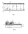
- FIG. 1 schematically depicts a band structure of a heterojunction SSL element, such as the SSL element shown in FIG. 2 .
- a valence band 110 which is typically located in a semiconductor material 210 doped with a p-type impurity is separated by a band gap 120 from a conduction band 130, which is typically located in a semiconductor material 230 doped with a n-type impurity.
- the valence band 110 exhibits conduction of electron holes 112 whereas the conduction band exhibits conduction of electrons 122, as is of course well-known.
- the band gap comprising multiple quantum wells or shallow states 122 is typically created by a quantum well material layer 220 in between the p-type semiconductor material 210 and the n-type semiconductor material 230.
- the quantum well material 220 typically further comprises deep trapping states 124.
- Shallow trapping states 122 derive their name from the close proximity to the band gap boundary, and often lie in the region between this boundary and the Fermi level. In contract, deep trapping states are relatively far away from both band gap boundaries, i.e. lie approximately in the middle of the band gap 120. Decay processes in the heterojunction involving shallow trapping states 122 are predominantly responsible for the radiative emission of heterojunction SSL elements, where direct (conduction) band to (valance) band emissive radiation plays no significant part (contrary to homo-junction SSL elements). A more detailed description of the recombination of electron-hole pairs in (heterojunction) SSL elements can be found in many textbooks and on-line resources; see e.g. https://courses.cit.cornell.edu/ece533/Lectures/handout7. pdf as retrieved from the Internet on 18 December 2012.
- FIG. 1 is a highly simplified representation of a band structure of a heterojunction SSL element.
- FIG. 2 is a highly simplified representation of such a heterojunction SSL element.
- the SSL element may comprise additional semiconductor layers and heterojunctions, Bragg reflectors, hole blocking layers, electron blocking layers and so on, which is all known per se in the art.
- any suitable materials may be chosen for the SSL element.
- the substrate 200 may be any suitable substrate such as a (transparent) sapphire substrate 200 in case the SSL element is arranged to emit light through the substrate 200 as indicated by the arrows in FIG. 2 .
- the semiconductor layers 210 and 230 may comprise any suitable semiconductor material, e.g. Ga-based semiconductor layers, e.g. AllnGaN, AllnGaP, and so on, with a multiple quantum well layer of e.g. GaN, InGaN and so on.
- the electrodes 240, 250 and optional separate sensing electrode 260 may take any suitable form and may be realized using any suitable electrically conductive material, e.g. suitable metals.
- the SSL element may comprise a driver architecture that can provide such a drive signal or may be connected to a current source, e.g. during binning procedures, that can provide the SSL element with such a current drive signal, as will be explained in more detail with the aid of FIG. 3 .
- an oscillating driving signal is fed into the SSL element, with or without a dc offset, and the response of the system is measured.
- the impedance (or admittance) can then be determined.
- Impedance can be converted into capacitance and conductance. By doing a frequency sweep at various temperatures, the conductance exhibits different peak positions at different temperatures when the frequency hits a resonance with the (shallow) donor levels.
- the shift in peak conductance corresponds to the emission rate, which then plotted in an Arrhenius plot gives information on the energy of the (full) band gap, as is explained in further detail by J.H. Zhao et al. in Applied Physics Letters 62, pages 2810-2812 (1993 ).
- thermal admittance spectroscopy it is known per se that at a fixed temperature, as the frequency of the test signal is reduced, deeper traps are able to respond and contribute to the capacitance and conductance. Similarly, as the temperature increases, the emission rate of a defect increases and the trap can contribute to the measured property at higher frequencies. At a threshold in frequency or temperature, the deep level appears as a step in the capacitance, or a peak in the conductance.
- the temperature of the inflection point of each plot of capacitance versus temperature at a fixed frequency is used along with the frequency, as one point in an Arrhenius plot.
- the energy of the defects can be obtained from plotting pairs of frequency and temperature points in an Arrhenius plot of emission rate (frequency of measurement) versus 1/ kT , in which T is temperature and k is the Bolzmann constant.
- the measured conductance will exhibit different peak positions at different temperatures when the frequency resonates with a shallow donor level or a deep trap state in the heterojunction of the SSL element.
- the energy levels of the various (shallow and deep) trap states can be determined by the construction of an Arrhenius plot as explained above.
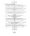
- the SSL element is brought to the required temperature for the TA measurement, after which the SSL element is subjected to the appropriate alternating current sweep in step 320, with the response of the SSL element to this alternating current sweep being determined in step 330.
- the SSL element may be brought to the required temperature by placing the SSL element in a heating stage and by monitoring the SSL element temperature using a temperature sensor, which may form part of the SSL element.
- the SSL element is brought to the desired temperature using the current waveform as disclosed in US 8,278,831 , and in particular paragraphs [0045]-[0062] of this application.
- the SSL element may comprise a first driver circuit adapted to provide its heterojunction with a first current output, wherein the first driver circuit has a control switch for interrupting the supply of the first current output, a second driver circuit for generating a second current output for driving the solid state lighting element, wherein the second driver circuit has a control switch for interrupting the supply of the second current output and wherein the output of the first current source driver comprises the combination of the first and second driver circuit outputs, in the form of a pulse width modulated output current which alternates between a high current including the first current output generated by the first driver circuit and a low current comprising the second current output generated by the second driver circuit.
- the thermal admittance current sweep i.e. an alternating current in which the frequency of the current is varied in a systematic manner, in step 320 may also be produced by this driver arrangement or by an additional driver arrangement in which a high current signal provides the required current sweep and a low current signal is used to sense the change in admittance, e.g. conductance or capacitance, across the heterojunction of the SSL element in step 330 to obtain the thermal admittance data.
- the driving electrodes 240, 250 of the SSL element are also used as sensing electrodes.
- the SSL element may alternatively comprise one or more separate sensing electrodes 260, in which case the change in admittance of the heterojunction caused by the alternating current sweep provided in step 320 is measured by one or more separate electrodes 260.
- the driver circuit for providing the alternating current sweep may simply generate this alternating current sweep without alternating this signal with a measurement current according to the teachings of US 8,278,831 .
- the exact electrode and driver arrangement of the SSL element chosen to implement the ability to generate a thermal admittance spectrum is not particularly limited; any suitable arrangement may be chosen.
- step 340 it is decided if the determination of the thermal admittance spectrum is complete, i.e. if the SSL element is subjected to the alternating current sweep, i.e. an alternating current in which the frequency of the current is varied in a systematic manner, at all targeted discrete temperatures. If this is not the case, the method reverts back to step 310, in which the SSL element temperature is adjusted to the next targeted temperature, after which steps 320 and 330 are repeated, i.e. the admittance data at the next targeted temperature is generated and obtained.
- the alternating current sweep i.e. an alternating current in which the frequency of the current is varied in a systematic manner
- step 350 in which the energies of the trap states identified in the thermal admittance spectrum are derived from the thermal admittance spectrum using Arrhenius plots as previously explained. This preferably is done automatically, e.g. using a suitably programmed data processor. Step 350 may further comprise identifying only shallow trap states from the thermal admittance spectrum in case the spectrum has been obtained by subjecting the heterojunction of the SSL element to appropriate bias voltages, as explained in more detail in the aforementioned paper by O.V. Kucherova et al.
- a deep level transient spectrum may be determined for the SSL element, which as is well known per se identifies deep trap states only, such that the state energies derived from the TA spectrum and the DLTS spectrum may be combined such that only the states that are unique to the TA spectrum are retained, as these are likely to be the shallow trap states in the band gap or multiple quantum well material 220.
- DLTS deep level transient spectrum
- the method may next proceed to step 370 to generate the estimated peak wavelength of the SSL element by determining the emission wavelength ⁇ of each shallow trapped state 122 and mapping these wavelengths as previously explained.
- the method first proceeds to step 360 prior to proceeding to step 370, in which the appropriate trap states are being selected using an empirically determined state selection threshold 140 as shown in FIG. 1 .
- the state selection threshold 140 defines the energy cut-off point at which states 122 are considered to be emissive states, such that all states 122 lying in between the state selection threshold 140 and the band gap boundary (in particular with the valence band) are considered emissive states.
- This for instance may be advantageous if it is not straightforward to detect which of the states identified in the TA spectrum are in fact shallow (quantum well) states, or in a scenario where the identified shallow states do not provide an accurate peak wavelength estimation of the SSL element, for instance because some dark states have erroneously been included or some emissive states have erroneously been excluded.
- steps 350, 360 and 370 are performed automatically, e.g. using a suitably programmed data processor.
- the state selection threshold 140 may be empirically determined using the benchmarking method shown in FIG. 4 .
- the peak wavelengths of a batch of SSL elements is determined in step 410 in a usual manner, i.e. by optically measuring the peak wavelength, as is of course well-known.
- the TA spectra of the SSL elements in this batch are also determined. It is noted that the order of steps 410 and 420 of course may be altered.
- an initial state selection threshold 140 is chosen, and the peak wavelengths of the SSL elements from the batch are estimated in step 450 from the trap states of the SSL elements selected in step 440 that are located in between the initial state selection threshold 140 and the band gap boundary as previously explained.
- the measured peak wavelength is compared to the estimated peak wavelength in step 460, and an average (absolute) deviation between the measured peak wavelengths and the estimated peak wavelengths is calculated.
- the estimated peak wavelengths are sufficiently accurate such that the state selection threshold 140 may be applied to further batches of SSL elements without having to optically determine the peak wavelength of the SSL elements of these further batches.
- the method reverts back to step 430, where the state selection threshold 140 is adjusted in accordance with the deviation information.
- the state selection threshold 140 is likely too low because higher energy trap states, which generate lower wavelength, i.e. blue-shifted light, have been erroneously omitted from the trap states selected in step 440 such that upon reverting back to step 430 the state selection threshold 140 is increased and steps 440, 450 and 460 are repeated with the increased state selection threshold 140.
- the state selection threshold 140 is likely too high because it has been wrongly assumed that higher energy trap states in the trap states selected in step 440 contributed to the emission spectrum of the SSL element such that upon reverting back to step 430 the state selection threshold 140 is decreased and steps 440, 450 and 460 are repeated with the decreased state selection threshold 140. This process is repeated until the average (absolute) deviation between the measured peak wavelengths and the estimated peak wavelengths becomes acceptable.
- steps 410, 420, 430, 440, 450 and 460 are performed automatically, e.g. using a suitably programmed data processor.
- the peak wavelength estimation method of the present invention may be advantageously applied in a binning process of SSL elements.
- the SSL elements are categorized (binned) such that SSL elements that share one or more characteristic properties, e.g. peak wavelengths, are grouped together, to ensure that a customer is provided with SSL elements that have the intended and desirable characteristics.
- step 510 An embodiment of a binning method according to the present invention is shown in FIG. 5 .
- step 510 the various bins (or categories) are defined in step 510, which bins are categorized based on peak wavelength information.
- step 520 for a SSL element from a batch of SSL elements, the peak wavelengths are estimated using TAS in accordance with an embodiment of the method as shown in FIG. 3 , after which in step 530 the SSL element is assigned to its appropriate bin based on its estimated peak wavelength. Steps 520 and 530 are repeated until all SSL elements from the batch have been assigned to one of the bins, as indicated in step 540.
- step 520 rather than estimating the peak wavelength of an individual SSL element in step 520, the peak wavelengths of all SSL elements in the batch may be estimated in step 520 prior to proceeding to step 530. In this embodiment, the method will revert back from step 540 to step 530 until all SSL elements have been categorized. Also, in this embodiment, step 520 may take place before step 510 without departing from the teachings of the present invention.
- steps 510, 520, 530 and 540 are performed automatically, e.g. using a suitably programmed data processor.
- the present application describes the method of electrically estimating a peak wavelength of a solid state lighting element in the context of binning procedures, it should be understood that this method may also be executed during the lifetime of the SSL element, e.g. to compensate for ageing or temperature effects. In such an embodiment, the measurement result may be used in a feedback mechanism to the driver circuits of the SSL element to compensate for such effects.
Landscapes
- Physics & Mathematics (AREA)
- Optics & Photonics (AREA)
- General Physics & Mathematics (AREA)
- Led Device Packages (AREA)
Abstract
Disclosed is a method of estimating a peak wavelength of a solid state lighting element, the method comprising determining (330) a thermal admittance spectrum of the solid state lighting element, said spectrum identifying the energy levels of the trap states in the band gap of the solid state lighting element; identifying (350) the shallow trap states in said spectrum; and estimating (370) said peak wavelength from the respective energy gaps between the identified shallow trap states and the band gap boundary. A binning method for characterizing solid state lighting elements utilizing this estimation method and a solid state lighting element adapted to implement this estimation method are also disclosed.
Description
- The present invention relates to a method of estimating the peak wavelength of a solid state lighting (SSL) element.
- The present invention further relates to a method of binning a plurality of SSL elements using the peak wavelength estimation method.
- The present invention yet further relates to a SSL element adapted to be subjected to such a peak wavelength estimation method.
- The present invention yet further relates to an apparatus comprising such a SSL element.
- Solid State Lighting (SSL), lighting using Light Emitting Diodes (LEDs), has become a fast growing research and development topic, as well as a large emerging market in recent years. This is because SSL offers many benefits, such as energy consumption reduction, improved quality of light, reliability and longer lifetime compared to e.g. incandescent lighting. This has caused SSL to enter a wide range of application domains, from general illumination devices, display devices to automotive applications.
- However, SSL elements face several fundamental challenges that originated from the way the SSL elements are manufactured. Even SSL elements from a single manufacturing batch can exhibit large variation in output wavelengths (peak wavelengths), output intensity and forward voltages. These variations have several causes.
- For instance, lattice mismatch between the layers of a (double) heterostructure, e.g. AllnGaN for green and blue SSL elements or AllnGaP for red SSL elements and the substrate such as a sapphire substrate results in the presence of intrinsic stress in the structure, which causes the presence of a large amount (∼1010 - 1012 cm-2) of defects; e.g. stochastic defects, such as stacking faults, threading dislocations, and interface states, which defects are present at the interfaces between the contacts and the SSL structure, between a buffer layer such as a GaN buffer layer and the Multiple Quantum Wells (MQW), and so on.
- Another source of such variations is material segregation; highly efficient light emitting quantum dots of various dimensions are present in the MQW due to local variations in Indium concentration in the layers defining the MQW. High internal electric fields, leading to Stark effect, can lead to variations in wavelengths of the emitted light, as can process variations across the wafer.
- These variations affect several aspects of SSL systems, such as the logistics of the produced SSLs. Because the end user typically demands a well-defined SSL system in terms of peak wavelength, flux output and forward voltage, the manufacturer of the SSL system has to apply expensive and time-consuming binning procedures to ensure that the SSL systems are grouped accordingly. In particular peak wavelength binning can be expensive as well as time-consuming, as this requires the optical measurement and subsequent interpretation of the output spectrum of the SSL elements, followed potentially by the adjustment of the control electronics of the SSL element to ensure that the SSL element produces light of the desired peak wavelength.
- The present invention seeks to provide a less expensive method of estimating a peak wavelength of a SSL element.
- The present invention further seeks to provide a less expensive SSL element peak wavelength binning method.
- The present invention further seeks to provide a SSL element that facilitates such less expensive peak wavelength estimation.
- The present invention further seeks to provide a device comprising such a SSL element.
- According to an aspect of the present invention, there is provided a method of electrically estimating a peak wavelength of a solid state lighting device, the method comprising determining a thermal admittance spectrum of the solid state lighting element, said spectrum identifying the energy levels of the trap states in the band gap of the solid state lighting element; identifying the shallow trap states in said spectrum; and estimating said peak wavelength from the respective energy gaps between the identified shallow trap states and the band gap boundary.
- The present invention is based on the known principle of applying thermal admittance spectroscopy (TAS) to determine the shallow and deep trap states of a SSL element. The present invention combines this known principle with the insight that in a typical SSL element the radiative relaxation from such trapped states predominantly occurs from shallow states, whereas deep states typically exhibit radiationless decay. Therefore, by identifying the shallow states or quantum wells in the bandgap material of the SSL element, the energy gap of the selected states to the band gap boundary can be used to generate an estimate of the intrinsic spectral composition of the light output of the SSL element including the peak wavelength of the SSL element, which may be identified as the wavelength associated with the highest number of identified shallow trap states. The method of the present invention therefore can provide peak wavelength information for a SSL element without requiring expensive optical detection techniques, thus reducing the cost associated with obtaining such peak wavelength information.
- In an embodiment, the step of determining the thermal admittance spectrum comprises repeating the steps of bringing the solid state lighting device to a desired temperature; exposing the solid state lighting device to an excitation current of varying frequency; and determining the change in the capacitance or conductance of the solid state lighting element as a function of said frequency.
- The step of bringing the solid state lighting device to a desired temperature may comprise exposing the solid state lighting element to a pulse width modulated current comprising a first component for driving the solid state lighting element and a second component for estimating the temperature of the solid state lighting element, which has the advantage that no separate heating stage is required to bring the SSL element to the desired temperature. Instead, the drive component of the pulse width modulated current can be used to heat the SSL element, whereas the measurement component may be used to estimate the temperature of the SSL element, as is explained in more detail in
US 8,278,831 . This allows for the accurate (±1 °C) and fast (∼10µs) measurement of SSL element temperature without the need for an external temperature sensor. Incidentally, the measurement component of the pulse width modulated current may instead or additionally be used to perform the admittance measurement of the SSL element, in which case the drive component of the pulse width modulated current may be used to provide the SSL element with the current waveform required for performing the thermal admittance spectroscopy. - In an embodiment, the method further comprises applying a state selection threshold to said spectrum to identify the shallow trap states located in between said state selection threshold and a band gap boundary. This is for instance advantageous when the shallow states or quantum wells cannot be easily identified in the TA spectrum or when the identified shallow states do not provide an accurate enough estimation of the peak wavelength of the SSL element. By applying a trap state selection using an empirically determined state selection threshold, the (shallow) trap states in the semiconductor material(s) of the SSL element that are most likely to exhibit emissive decay can be selected from all the states detected by TAS.
- In an embodiment, said state selection threshold may be determined using a benchmarking procedure that comprises optically measuring the respective peak wavelengths of a plurality of solid state lighting elements; for each solid state lighting element of said plurality, determining its thermal admittance spectrum; and applying a fitting algorithm to the plurality of thermal admittance spectra to determine a state selection threshold for which the average of the respective peak wavelengths estimated from the respective energy gaps of the trap states in said spectra that are located in between said threshold and the band gap boundary deviates from the average of the measured respective peak wavelengths by less than a predefined threshold.
- This approach can be followed because different batches of the same product tend to exhibit comparable defect characteristics and spreads, such that once a state selection threshold is found for a batch of SSL elements that selects a set of trap states such that the estimated peak wavelength of each SSL element accurately corresponds to the measured peak wavelength of the SSL element, this state selection threshold can be applied to other batches of the same SSL element.
- In accordance with another aspect of the present invention, there is provided a method of binning a plurality of solid state lighting elements into a plurality of bins characterised by peak wavelength, the method comprising estimating the peak wavelength of each solid state lighting element by an embodiment of the peak wavelength estimation method of the present invention; and assigning the solid state lighting element to one of said bins based on the estimated peak wavelength.
- This binning method benefits from the ability to accurately estimate a peak wavelength of an individual SSL element electrically in that the binning procedure can be performed more quickly and more cost effectively without compromising customer requirements.
- According to yet another aspect of the present invention, there is provided a solid state lighting element comprising a heterojunction defined by a quantum well material layer sandwiched between an n-type semiconductor layer and a p-type semiconductor layer; a first current source driver adapted to provide said heterojunction with a first current output during an operating mode of the solid state lighting element; a second current source driver adapted to provide said heterojunction with a variable frequency current output during a peak wavelength estimation mode of the solid state lighting element; and at least one sensing electrode in conductive contact with said heterojunction adapted to measure the change in capacitance or conductance across said heterojunction. Such a SSL element advantageously facilitates the measurement of a TAS, which allows for a more efficient binning of the SSL element, as previously explained.
- The first current source driver and the second current source driver may be different current source drivers, e.g. may be provided as separate current drivers, or may be the same current source driver, i.e. a single current source driver combining the functionality of the first and second current source drivers.
- In an embodiment, the first current source driver comprises a first driver circuit adapted to provide said heterojunction with the first current output, wherein the first driver circuit has a control switch for interrupting the supply of the first current output; a second driver circuit for generating a second current output for driving the solid state lighting element, wherein the second driver circuit has a control switch for interrupting the supply of the second current output; and wherein the output of the first current source driver comprises the combination of the first and second driver circuit outputs, in the form of a pulse width modulated output current which alternates between a high current including the first current output generated by the first driver circuit and a low current comprising the second current output generated by the second driver circuit.
- Such a first current source driver is known per se from
US 8,278,831 and may be used to control the junction temperature of the SSL element in a sensorless manner, as explained in more detail in this prior art application. - Alternatively, the solid state lighting element may comprise a temperature sensor to measure the increase in (junction) temperature of the SSL element, e.g. during the determination of the thermal admittance spectrum of the SSL element.
- The solid state lighting element preferably comprises a light emitting diode.
- In accordance with a further embodiment of the present invention, there is provided a device comprising the solid state lighting element according to an embodiment of the present invention. Such a device benefits from the fact that the SSL element can be manufactured more cost-effectively as previously explained. Such a device may for instance be a lighting device, a display device, an automotive device and so on.
- Embodiments of the invention are described in more detail and by way of nonlimiting examples with reference to the accompanying drawings, wherein:
-
FIG. 1 schematically depicts a band structure of a heterojunction SSL element; -
FIG. 2 schematically depicts an aspect of a SSL element according to an embodiment of the present invention; -
FIG. 3 depicts a flow chart of a method of estimating a peak wavelength of an SSL element according to an embodiment of the present invention; -
FIG. 4 depicts a flow chart of a method of determining a state selection threshold for use in the method ofFIG. 3 ; and -
FIG. 5 depicts a flow chart of a SSL element binning method according to an embodiment of the present invention. - It should be understood that the Figures are merely schematic and are not drawn to scale. It should also be understood that the same reference numerals are used throughout the Figures to indicate the same or similar parts.
-
FIG. 1 schematically depicts a band structure of a heterojunction SSL element, such as the SSL element shown inFIG. 2 . Avalence band 110, which is typically located in asemiconductor material 210 doped with a p-type impurity is separated by aband gap 120 from aconduction band 130, which is typically located in asemiconductor material 230 doped with a n-type impurity. Thevalence band 110 exhibits conduction ofelectron holes 112 whereas the conduction band exhibits conduction ofelectrons 122, as is of course well-known. The band gap comprising multiple quantum wells orshallow states 122 is typically created by a quantumwell material layer 220 in between the p-type semiconductor material 210 and the n-type semiconductor material 230. Thequantum well material 220 typically further comprisesdeep trapping states 124. - Shallow trapping states 122 derive their name from the close proximity to the band gap boundary, and often lie in the region between this boundary and the Fermi level. In contract, deep trapping states are relatively far away from both band gap boundaries, i.e. lie approximately in the middle of the
band gap 120. Decay processes in the heterojunction involving shallow trapping states 122 are predominantly responsible for the radiative emission of heterojunction SSL elements, where direct (conduction) band to (valance) band emissive radiation plays no significant part (contrary to homo-junction SSL elements). A more detailed description of the recombination of electron-hole pairs in (heterojunction) SSL elements can be found in many textbooks and on-line resources; see e.g. https://courses.cit.cornell.edu/ece533/Lectures/handout7. pdf as retrieved from the Internet on 18 December 2012. - Hence, by determining the energy ΔE of the shallow trap states 122 relative to the band gap boundary, an estimate of the wavelength λ of the radiative emission from the shallow trapped state can be given from ΔE = hc/λ, in which h is Planck's constant and c is the speed of light. By determining the emission wavelength λ of each shallow
trapped state 122 and mapping these wavelengths, an estimated radiative emission spectrum of the SSL element is compiled that serves as an estimation of the peak wavelength of the SSL element. More particularly, the peak wavelength may be identified as the wavelength that is associated with the largest number of mapped shallow trap states. - It should be appreciated that
FIG. 1 is a highly simplified representation of a band structure of a heterojunction SSL element. Similarly,FIG. 2 is a highly simplified representation of such a heterojunction SSL element. For instance, the SSL element may comprise additional semiconductor layers and heterojunctions, Bragg reflectors, hole blocking layers, electron blocking layers and so on, which is all known per se in the art. Also, any suitable materials may be chosen for the SSL element. For instance, thesubstrate 200 may be any suitable substrate such as a (transparent)sapphire substrate 200 in case the SSL element is arranged to emit light through thesubstrate 200 as indicated by the arrows inFIG. 2 . - The semiconductor layers 210 and 230 may comprise any suitable semiconductor material, e.g. Ga-based semiconductor layers, e.g. AllnGaN, AllnGaP, and so on, with a multiple quantum well layer of e.g. GaN, InGaN and so on. The
electrodes separate sensing electrode 260 may take any suitable form and may be realized using any suitable electrically conductive material, e.g. suitable metals. - Many suitable materials have been well-documented, and it should be understood that the present invention is not limited to a SSL element having a particular type of structure with a particular combination of materials. Instead, the present invention is based on the insight that a SSL element may be adapted such that it can be driven to provide admittance spectroscopy data, from which peak wavelength information may be derived. The SSL element may comprise a driver architecture that can provide such a drive signal or may be connected to a current source, e.g. during binning procedures, that can provide the SSL element with such a current drive signal, as will be explained in more detail with the aid of
FIG. 3 . - To perform thermal admittance spectroscopy, an oscillating driving signal is fed into the SSL element, with or without a dc offset, and the response of the system is measured. The impedance (or admittance) can then be determined. Impedance can be converted into capacitance and conductance. By doing a frequency sweep at various temperatures, the conductance exhibits different peak positions at different temperatures when the frequency hits a resonance with the (shallow) donor levels. The shift in peak conductance corresponds to the emission rate, which then plotted in an Arrhenius plot gives information on the energy of the (full) band gap, as is explained in further detail by J.H. Zhao et al. in Applied Physics Letters 62, pages 2810-2812 (1993).
- In thermal admittance spectroscopy, it is known per se that at a fixed temperature, as the frequency of the test signal is reduced, deeper traps are able to respond and contribute to the capacitance and conductance. Similarly, as the temperature increases, the emission rate of a defect increases and the trap can contribute to the measured property at higher frequencies. At a threshold in frequency or temperature, the deep level appears as a step in the capacitance, or a peak in the conductance. The temperature of the inflection point of each plot of capacitance versus temperature at a fixed frequency is used along with the frequency, as one point in an Arrhenius plot. The energy of the defects can be obtained from plotting pairs of frequency and temperature points in an Arrhenius plot of emission rate (frequency of measurement) versus 1/kT, in which T is temperature and k is the Bolzmann constant.
- It is furthermore well-known, see e.g. O.V. Kucherova et al. in Inorganic Materials, Vol. 47(14), pages 1574-1578 (2011) that in TAS, the amplitude of the spectral peaks from quantum wells exhibit a sharp dependence on the bias applied to the material, such that the emission from quantum wells can be reliably distinguished from emissions from a deep trap state, e.g. a bulk deep centre.
- Hence, by performing a frequency sweep at various temperatures and various bias conditions, the measured conductance will exhibit different peak positions at different temperatures when the frequency resonates with a shallow donor level or a deep trap state in the heterojunction of the SSL element. The energy levels of the various (shallow and deep) trap states can be determined by the construction of an Arrhenius plot as explained above.
- Hence, in
step 310 of the peak wavelength estimation method shown inFIG. 3 , the SSL element is brought to the required temperature for the TA measurement, after which the SSL element is subjected to the appropriate alternating current sweep instep 320, with the response of the SSL element to this alternating current sweep being determined instep 330. This may be realized in a number of ways. For instance, the SSL element may be brought to the required temperature by placing the SSL element in a heating stage and by monitoring the SSL element temperature using a temperature sensor, which may form part of the SSL element. - However, in a preferred alternative embodiment, the SSL element is brought to the desired temperature using the current waveform as disclosed in
US 8,278,831 , and in particular paragraphs [0045]-[0062] of this application. To this end, the SSL element may comprise a first driver circuit adapted to provide its heterojunction with a first current output, wherein the first driver circuit has a control switch for interrupting the supply of the first current output, a second driver circuit for generating a second current output for driving the solid state lighting element, wherein the second driver circuit has a control switch for interrupting the supply of the second current output and wherein the output of the first current source driver comprises the combination of the first and second driver circuit outputs, in the form of a pulse width modulated output current which alternates between a high current including the first current output generated by the first driver circuit and a low current comprising the second current output generated by the second driver circuit. - The thermal admittance current sweep, i.e. an alternating current in which the frequency of the current is varied in a systematic manner, in
step 320 may also be produced by this driver arrangement or by an additional driver arrangement in which a high current signal provides the required current sweep and a low current signal is used to sense the change in admittance, e.g. conductance or capacitance, across the heterojunction of the SSL element instep 330 to obtain the thermal admittance data. In this embodiment, the drivingelectrodes separate sensing electrodes 260, in which case the change in admittance of the heterojunction caused by the alternating current sweep provided instep 320 is measured by one or moreseparate electrodes 260. In this embodiment, the driver circuit for providing the alternating current sweep may simply generate this alternating current sweep without alternating this signal with a measurement current according to the teachings ofUS 8,278,831 . The exact electrode and driver arrangement of the SSL element chosen to implement the ability to generate a thermal admittance spectrum is not particularly limited; any suitable arrangement may be chosen. - In
step 340, it is decided if the determination of the thermal admittance spectrum is complete, i.e. if the SSL element is subjected to the alternating current sweep, i.e. an alternating current in which the frequency of the current is varied in a systematic manner, at all targeted discrete temperatures. If this is not the case, the method reverts back to step 310, in which the SSL element temperature is adjusted to the next targeted temperature, after which steps 320 and 330 are repeated, i.e. the admittance data at the next targeted temperature is generated and obtained. - Once the admittance data at all targeted discrete temperatures has been obtained, the method proceeds to step 350 in which the energies of the trap states identified in the thermal admittance spectrum are derived from the thermal admittance spectrum using Arrhenius plots as previously explained. This preferably is done automatically, e.g. using a suitably programmed data processor. Step 350 may further comprise identifying only shallow trap states from the thermal admittance spectrum in case the spectrum has been obtained by subjecting the heterojunction of the SSL element to appropriate bias voltages, as explained in more detail in the aforementioned paper by O.V. Kucherova et al.
- Alternatively, in case it proves cumbersome to separate the shallow trap states from the deep trap states in this manner, a deep level transient spectrum (DLTS) may be determined for the SSL element, which as is well known per se identifies deep trap states only, such that the state energies derived from the TA spectrum and the DLTS spectrum may be combined such that only the states that are unique to the TA spectrum are retained, as these are likely to be the shallow trap states in the band gap or multiple
quantum well material 220. - In an embodiment, the method may next proceed to step 370 to generate the estimated peak wavelength of the SSL element by determining the emission wavelength λ of each shallow
trapped state 122 and mapping these wavelengths as previously explained. - In an alternative embodiment, the method first proceeds to step 360 prior to proceeding to step 370, in which the appropriate trap states are being selected using an empirically determined
state selection threshold 140 as shown inFIG. 1 . Thestate selection threshold 140 defines the energy cut-off point at which states 122 are considered to be emissive states, such that all states 122 lying in between thestate selection threshold 140 and the band gap boundary (in particular with the valence band) are considered emissive states. This for instance may be advantageous if it is not straightforward to detect which of the states identified in the TA spectrum are in fact shallow (quantum well) states, or in a scenario where the identified shallow states do not provide an accurate peak wavelength estimation of the SSL element, for instance because some dark states have erroneously been included or some emissive states have erroneously been excluded. - At this point it is noted that preferably at least some and more preferably all of
steps - In an embodiment, the
state selection threshold 140 may be empirically determined using the benchmarking method shown inFIG. 4 . In this method, the peak wavelengths of a batch of SSL elements is determined instep 410 in a usual manner, i.e. by optically measuring the peak wavelength, as is of course well-known. Instep 420, the TA spectra of the SSL elements in this batch are also determined. It is noted that the order ofsteps - Next, an initial
state selection threshold 140 is chosen, and the peak wavelengths of the SSL elements from the batch are estimated instep 450 from the trap states of the SSL elements selected instep 440 that are located in between the initialstate selection threshold 140 and the band gap boundary as previously explained. For each SSL element, the measured peak wavelength is compared to the estimated peak wavelength instep 460, and an average (absolute) deviation between the measured peak wavelengths and the estimated peak wavelengths is calculated. - In case the average (absolute) deviation falls below a predefined value, the estimated peak wavelengths are sufficiently accurate such that the
state selection threshold 140 may be applied to further batches of SSL elements without having to optically determine the peak wavelength of the SSL elements of these further batches. In case the average (absolute) deviation falls below a predefined value, the method reverts back to step 430, where thestate selection threshold 140 is adjusted in accordance with the deviation information. - If the averaged peak wavelength comparison has indicated that the estimated peak wavelengths are predominantly red-shifted compared to the measured peak wavelengths, the
state selection threshold 140 is likely too low because higher energy trap states, which generate lower wavelength, i.e. blue-shifted light, have been erroneously omitted from the trap states selected instep 440 such that upon reverting back to step 430 thestate selection threshold 140 is increased andsteps state selection threshold 140. - If the averaged peak wavelength comparison has indicated that the estimated peak wavelengths are predominantly blue-shifted compared to the measured peak wavelengths, the
state selection threshold 140 is likely too high because it has been wrongly assumed that higher energy trap states in the trap states selected instep 440 contributed to the emission spectrum of the SSL element such that upon reverting back to step 430 thestate selection threshold 140 is decreased andsteps state selection threshold 140. This process is repeated until the average (absolute) deviation between the measured peak wavelengths and the estimated peak wavelengths becomes acceptable. - At this point it is noted that preferably at least some and more preferably all of
steps - The peak wavelength estimation method of the present invention may be advantageously applied in a binning process of SSL elements. In a binning process, the SSL elements are categorized (binned) such that SSL elements that share one or more characteristic properties, e.g. peak wavelengths, are grouped together, to ensure that a customer is provided with SSL elements that have the intended and desirable characteristics.
- An embodiment of a binning method according to the present invention is shown in
FIG. 5 . First, the various bins (or categories) are defined instep 510, which bins are categorized based on peak wavelength information. Next instep 520, for a SSL element from a batch of SSL elements, the peak wavelengths are estimated using TAS in accordance with an embodiment of the method as shown inFIG. 3 , after which instep 530 the SSL element is assigned to its appropriate bin based on its estimated peak wavelength.Steps step 540. - It should be understood that many alternatives to the above binning method will be immediately apparent to the skilled person. For instance, rather than estimating the peak wavelength of an individual SSL element in
step 520, the peak wavelengths of all SSL elements in the batch may be estimated instep 520 prior to proceeding to step 530. In this embodiment, the method will revert back fromstep 540 to step 530 until all SSL elements have been categorized. Also, in this embodiment, step 520 may take place beforestep 510 without departing from the teachings of the present invention. - At this point it is noted that preferably at least some and more preferably all of
steps - Finally, it is noted that although the present application describes the method of electrically estimating a peak wavelength of a solid state lighting element in the context of binning procedures, it should be understood that this method may also be executed during the lifetime of the SSL element, e.g. to compensate for ageing or temperature effects. In such an embodiment, the measurement result may be used in a feedback mechanism to the driver circuits of the SSL element to compensate for such effects.
- It should be noted that the above-mentioned embodiments illustrate rather than limit the invention, and that those skilled in the art will be able to design many alternative embodiments without departing from the scope of the appended claims. In the claims, any reference signs placed between parentheses shall not be construed as limiting the claim. The word "comprising" does not exclude the presence of elements or steps other than those listed in a claim. The word "a" or "an" preceding an element does not exclude the presence of a plurality of such elements. The invention can be implemented by means of hardware comprising several distinct elements. In the device claim enumerating several means, several of these means can be embodied by one and the same item of hardware. The mere fact that certain measures are recited in mutually different dependent claims does not indicate that a combination of these measures cannot be used to advantage.
Claims (14)
- A method of electrically estimating a peak wavelength of a solid state lighting element, the method comprising:determining a thermal admittance spectrum of the solid state lighting element, said spectrum identifying the energy levels of the trap states in the band gap of the solid state lighting element;identifying the shallow trap states in said spectrum; andestimating said peak wavelength from the respective energy gaps between the identified shallow trap states and the band gap boundary.
- The method of claim 1, wherein the step of determining the thermal admittance spectrum comprises repeating the steps of:bringing the solid state element to a desired temperature;exposing the solid state lighting device to an excitation current of varying frequency; anddetermining the change in the capacitance or conductance of the solid state lighting element as a function of said frequency.
- The method of claim 2, wherein the step of bringing the solid state lighting device to a desired temperature comprises exposing the solid state lighting element to a pulse width modulated current comprising a first component for driving the solid state lighting element and a second component for estimating the temperature of the solid state lighting element.
- The method of claim 2 or 3, further comprising varying a bias applied to the solid state lighting element to identify said shallow trap states in the thermal admittance spectrum.
- The method of any of claims 1-3, further comprising applying a state selection threshold to said spectrum to identify the shallow trap states located in between said state selection threshold and a band gap boundary.
- The method of claim 5, further comprising defining said state selection threshold by:optically measuring the respective peak wavelengths of a plurality of solid state lighting elements;for each solid state lighting element of said plurality, determining its thermal admittance spectrum; andapplying a fitting algorithm to the plurality of thermal admittance spectra to determine a state selection threshold for which the average of the respective peak wavelengths estimated from the respective energy gaps of the trap states in said spectra that are located in between said threshold and the band gap boundary deviates from the average of the measured respective peak wavelengths by less than a predefined threshold.
- A method of binning a plurality of solid state lighting elements into a plurality of bins characterised by peak wavelength, the method comprising:electrically estimating the peak wavelength of each solid state lighting element by the method of any of claims 1-6; andassigning the solid state lighting element to one of said bins based on the estimated peak wavelength.
- A solid state lighting element comprising:a heterojunction defined by a quantum well material layer sandwiched between an n-type semiconductor layer and a p-type semiconductor layer;a first current source driver adapted to provide said heterojunction with a first current output during an operating mode of the solid state lighting element;a second current source driver adapted to provide said heterojunction with a variable frequency current output during a peak wavelength estimation mode of the solid state lighting element;at least one sensing electrode in conductive contact with said heterojunction adapted to measure the change in capacitance or conductance across said heterojunction.
- The solid state lighting element of claim 8, wherein the first current source driver and the second current source driver are different current source drivers.
- The solid state lighting element of claim 8, wherein the first current source driver and the second current source driver are the same current source driver.
- The solid state lighting element of any of claims 8-10, wherein the first current source driver comprises:a first driver circuit adapted to provide said heterojunction with the first current output, wherein the first driver circuit has a control switch for interrupting the supply of the first current output;a second driver circuit for generating a second current output for driving the solid state lighting element, wherein the second driver circuit has a control switch for interrupting the supply of the second current output; andwherein the output of the first current source driver comprises the combination of the first and second driver circuit outputs, in the form of a pulse width modulated output current which alternates between a high current including the first current output generated by the first driver circuit and a low current comprising the second current output generated by the second driver circuit.
- The solid state lighting element of any of claims 8-10, further comprising a temperature sensor.
- The solid state lighting element of any of claims 8-12, wherein the solid state lighting element comprises a light emitting diode.
- A device comprising the solid state lighting element of any of claims 8-13.
Priority Applications (1)
| Application Number | Priority Date | Filing Date | Title |
|---|---|---|---|
| EP12198633.5A EP2746792A1 (en) | 2012-12-20 | 2012-12-20 | Solid state lighting element, peak wavelength estimation method and binning method |
Applications Claiming Priority (1)
| Application Number | Priority Date | Filing Date | Title |
|---|---|---|---|
| EP12198633.5A EP2746792A1 (en) | 2012-12-20 | 2012-12-20 | Solid state lighting element, peak wavelength estimation method and binning method |
Publications (1)
| Publication Number | Publication Date |
|---|---|
| EP2746792A1 true EP2746792A1 (en) | 2014-06-25 |
Family
ID=47627923
Family Applications (1)
| Application Number | Title | Priority Date | Filing Date |
|---|---|---|---|
| EP12198633.5A Withdrawn EP2746792A1 (en) | 2012-12-20 | 2012-12-20 | Solid state lighting element, peak wavelength estimation method and binning method |
Country Status (1)
| Country | Link |
|---|---|
| EP (1) | EP2746792A1 (en) |
Citations (1)
| Publication number | Priority date | Publication date | Assignee | Title |
|---|---|---|---|---|
| US20100315019A1 (en) * | 2008-01-28 | 2010-12-16 | Nxp B.V. | Led driver circuit and method, and system and method for estimating the junction temperature of a light emitting diode |
-
2012
- 2012-12-20 EP EP12198633.5A patent/EP2746792A1/en not_active Withdrawn
Patent Citations (2)
| Publication number | Priority date | Publication date | Assignee | Title |
|---|---|---|---|---|
| US20100315019A1 (en) * | 2008-01-28 | 2010-12-16 | Nxp B.V. | Led driver circuit and method, and system and method for estimating the junction temperature of a light emitting diode |
| US8278831B2 (en) | 2008-01-28 | 2012-10-02 | Nxp B.V. | LED driver circuit and method, and system and method for estimating the junction temperature of a light emitting diode |
Non-Patent Citations (8)
| Title |
|---|
| FARHAN RANA,: "Semiconductor Light Emitting Diodes and Solid State Lighting", 18 December 2012 (2012-12-18), pages 1 - 19, XP055076384, Retrieved from the Internet <URL:https://courses.cit.cornell.edu/ece533/Lectures/handout7.pdf> [retrieved on 20130826] * |
| J. H. ZHAO ET AL: "Admittance spectroscopy characterization of InP/InGaAsP single quantum wells grown by low-pressure metalorganic chemical vapor deposition", APPLIED PHYSICS LETTERS, vol. 62, no. 22, 1 January 1993 (1993-01-01), pages 2810, XP055076376, ISSN: 0003-6951, DOI: 10.1063/1.109217 * |
| J.H. ZHAO ET AL., APPLIED PHYSICS LETTERS, vol. 62, 1993, pages 2810 - 2812 |
| KUCHEROVA O V ET AL: "Nondestructive diagnostics of nanoheterostructures with InGaN/GaN multiple quantum wells by thermal admittance spectroscopy", INORGANIC MATERIALS, NAUKA/INTERPERIODICA, MO, vol. 47, no. 14, 20 November 2011 (2011-11-20), pages 1574 - 1578, XP019980624, ISSN: 1608-3172, DOI: 10.1134/S0020168511140111 * |
| NGUYEN N D ET AL: "Thermal admittance spectroscopy of Mg-doped GaN Schottky diodes", JOURNAL OF APPLIED PHYSICS, AMERICAN INSTITUTE OF PHYSICS. NEW YORK, US, vol. 90, no. 2, 15 July 2001 (2001-07-15), pages 985 - 993, XP012053871, ISSN: 0021-8979, DOI: 10.1063/1.1379345 * |
| O.V. KUCHEROVA ET AL., INORGANIC MATERIALS, vol. 47, no. 14, 2011, pages 1574 - 1578 |
| PAVESI M ET AL: "A new approach to correlate transport processes and optical efficiency in GaN-based LEDs", JOURNAL OF PHYSICS D. APPLIED PHYSICS, IOP PUBLISHING, BRISTOL, GB, vol. 42, no. 4, 21 February 2009 (2009-02-21), pages 45110, XP020149173, ISSN: 0022-3727, DOI: 10.1088/0022-3727/42/4/045110 * |
| SCHIFANO R ET AL: "Shallow levels in virgin hydrothermally grown n-type ZnO studied by thermal admittance spectroscopy", PHYSICA B. CONDENSED MATTER, AMSTERDAM, NL, vol. 404, no. 22, 1 December 2009 (2009-12-01), pages 4344 - 4348, XP026719499, ISSN: 0921-4526, [retrieved on 20090910], DOI: 10.1016/J.PHYSB.2009.09.030 * |
Similar Documents
| Publication | Publication Date | Title |
|---|---|---|
| Espenlaub et al. | Evidence of trap-assisted Auger recombination in low radiative efficiency MBE-grown III-nitride LEDs | |
| Monti et al. | Defect-related degradation of AlGaN-based UV-B LEDs | |
| CN110337712A (en) | Light emitting diode (LED) test equipment and manufacturing method | |
| EP2230884B1 (en) | Method of controlling an LED, and an LED controller | |
| JP6075257B2 (en) | Inspection method and inspection apparatus for silicon carbide semiconductor device | |
| CN101561475A (en) | Method and device for non-contact detection of LED luminescence properties | |
| US9551669B2 (en) | Method and system for characterizing light emitting devices | |
| US12203971B2 (en) | Apparatus and method for inspecting light-emitting diode dies | |
| Pralgauskaitė et al. | Reliability investigation of light-emitting diodes via low frequency noise characteristics | |
| KR101116840B1 (en) | Method and Apparatus for Measuring Internal Quantum Well Efficiency of LED | |
| Herzog et al. | Lifetime prediction of current-and temperature-induced degradation in silicone-encapsulated 365 nm high-power light-emitting diodes | |
| Alexeev et al. | Dynamic response-based LEDs health and temperature monitoring | |
| Renso et al. | Understanding the degradation processes of GaN based LEDs submitted to extremely high current density | |
| Herzog et al. | Efficiency droop in green InGaN/GaN light emitting diodes: Degradation mechanisms and initial characteristics | |
| Polyakov et al. | Deep trap analysis in green light emitting diodes: Problems and solutions | |
| JP2007088389A (en) | Apparatus and method for measuring internal quantum efficiency of semiconductor light emitting device | |
| Herzog et al. | Monitoring the optical degradation of green light-emitting diodes on the basis of measured electrical characteristics | |
| EP2746792A1 (en) | Solid state lighting element, peak wavelength estimation method and binning method | |
| JP2008227463A (en) | Light-emitting element inspection method and inspection apparatus, and burn-in method and burn-in apparatus | |
| KR101513242B1 (en) | Method and Apparatus for Measuring Internal Quantum Efficiency of LED | |
| KR101720165B1 (en) | Apparatus and method for analyzing state density of light emitting diode | |
| Glemža et al. | Low-frequency noise characteristics of high-power white LED during long-term aging experiment | |
| WO2010049882A2 (en) | Lighting unit with temperature protection | |
| Hamon et al. | N-contacts degradation analysis of white flip chip LEDs during reliability tests | |
| De Santi et al. | Variations in junction capacitance and doping activation associated with electrical stress of InGaN/GaN laser diodes |
Legal Events
| Date | Code | Title | Description |
|---|---|---|---|
| PUAI | Public reference made under article 153(3) epc to a published international application that has entered the european phase |
Free format text: ORIGINAL CODE: 0009012 |
|
| 17P | Request for examination filed |
Effective date: 20121220 |
|
| AK | Designated contracting states |
Kind code of ref document: A1 Designated state(s): AL AT BE BG CH CY CZ DE DK EE ES FI FR GB GR HR HU IE IS IT LI LT LU LV MC MK MT NL NO PL PT RO RS SE SI SK SM TR |
|
| AX | Request for extension of the european patent |
Extension state: BA ME |
|
| STAA | Information on the status of an ep patent application or granted ep patent |
Free format text: STATUS: THE APPLICATION IS DEEMED TO BE WITHDRAWN |
|
| 18D | Application deemed to be withdrawn |
Effective date: 20150106 |