EP2745295B1 - Apparatus and methods including source gates - Google Patents
Apparatus and methods including source gates Download PDFInfo
- Publication number
- EP2745295B1 EP2745295B1 EP12824349.0A EP12824349A EP2745295B1 EP 2745295 B1 EP2745295 B1 EP 2745295B1 EP 12824349 A EP12824349 A EP 12824349A EP 2745295 B1 EP2745295 B1 EP 2745295B1
- Authority
- EP
- European Patent Office
- Prior art keywords
- charge storage
- strings
- source
- block
- storage devices
- Prior art date
- Legal status (The legal status is an assumption and is not a legal conclusion. Google has not performed a legal analysis and makes no representation as to the accuracy of the status listed.)
- Active
Links
- 238000000034 method Methods 0.000 title description 5
- XUIMIQQOPSSXEZ-UHFFFAOYSA-N Silicon Chemical compound [Si] XUIMIQQOPSSXEZ-UHFFFAOYSA-N 0.000 claims description 53
- 229910052710 silicon Inorganic materials 0.000 claims description 53
- 239000010703 silicon Substances 0.000 claims description 53
- 239000004065 semiconductor Substances 0.000 claims description 44
- 239000000758 substrate Substances 0.000 claims description 18
- 238000009792 diffusion process Methods 0.000 claims description 15
- 229910021420 polycrystalline silicon Inorganic materials 0.000 claims description 12
- 229920005591 polysilicon Polymers 0.000 claims description 12
- 239000000463 material Substances 0.000 claims description 11
- 238000007667 floating Methods 0.000 claims description 10
- 238000010276 construction Methods 0.000 description 29
- VYPSYNLAJGMNEJ-UHFFFAOYSA-N Silicium dioxide Chemical compound O=[Si]=O VYPSYNLAJGMNEJ-UHFFFAOYSA-N 0.000 description 28
- 239000000377 silicon dioxide Substances 0.000 description 14
- PXHVJJICTQNCMI-UHFFFAOYSA-N Nickel Chemical compound [Ni] PXHVJJICTQNCMI-UHFFFAOYSA-N 0.000 description 12
- 235000012239 silicon dioxide Nutrition 0.000 description 9
- 229910052751 metal Inorganic materials 0.000 description 8
- 239000002184 metal Substances 0.000 description 8
- 239000010936 titanium Substances 0.000 description 8
- 238000010586 diagram Methods 0.000 description 6
- 230000000694 effects Effects 0.000 description 6
- WFKWXMTUELFFGS-UHFFFAOYSA-N tungsten Chemical compound [W] WFKWXMTUELFFGS-UHFFFAOYSA-N 0.000 description 6
- 229910052721 tungsten Inorganic materials 0.000 description 6
- 239000010937 tungsten Substances 0.000 description 6
- RTAQQCXQSZGOHL-UHFFFAOYSA-N Titanium Chemical compound [Ti] RTAQQCXQSZGOHL-UHFFFAOYSA-N 0.000 description 4
- 239000010941 cobalt Substances 0.000 description 4
- 229910017052 cobalt Inorganic materials 0.000 description 4
- GUTLYIVDDKVIGB-UHFFFAOYSA-N cobalt atom Chemical compound [Co] GUTLYIVDDKVIGB-UHFFFAOYSA-N 0.000 description 4
- 230000008878 coupling Effects 0.000 description 4
- 238000010168 coupling process Methods 0.000 description 4
- 238000005859 coupling reaction Methods 0.000 description 4
- 229910052759 nickel Inorganic materials 0.000 description 4
- 229910052715 tantalum Inorganic materials 0.000 description 4
- GUVRBAGPIYLISA-UHFFFAOYSA-N tantalum atom Chemical compound [Ta] GUVRBAGPIYLISA-UHFFFAOYSA-N 0.000 description 4
- 229910052719 titanium Inorganic materials 0.000 description 4
- 230000002093 peripheral effect Effects 0.000 description 3
- ZOXJGFHDIHLPTG-UHFFFAOYSA-N Boron Chemical compound [B] ZOXJGFHDIHLPTG-UHFFFAOYSA-N 0.000 description 2
- 229910052581 Si3N4 Inorganic materials 0.000 description 2
- 229910052796 boron Inorganic materials 0.000 description 2
- 230000005672 electromagnetic field Effects 0.000 description 2
- BHEPBYXIRTUNPN-UHFFFAOYSA-N hydridophosphorus(.) (triplet) Chemical compound [PH] BHEPBYXIRTUNPN-UHFFFAOYSA-N 0.000 description 2
- HQVNEWCFYHHQES-UHFFFAOYSA-N silicon nitride Chemical compound N12[Si]34N5[Si]62N3[Si]51N64 HQVNEWCFYHHQES-UHFFFAOYSA-N 0.000 description 2
- 238000003491 array Methods 0.000 description 1
- 230000000903 blocking effect Effects 0.000 description 1
- 230000001413 cellular effect Effects 0.000 description 1
- 238000004891 communication Methods 0.000 description 1
- 230000005670 electromagnetic radiation Effects 0.000 description 1
- 230000006870 function Effects 0.000 description 1
- 230000003287 optical effect Effects 0.000 description 1
Images


Classifications
-
- G—PHYSICS
- G11—INFORMATION STORAGE
- G11C—STATIC STORES
- G11C16/00—Erasable programmable read-only memories
- G11C16/02—Erasable programmable read-only memories electrically programmable
- G11C16/04—Erasable programmable read-only memories electrically programmable using variable threshold transistors, e.g. FAMOS
- G11C16/0483—Erasable programmable read-only memories electrically programmable using variable threshold transistors, e.g. FAMOS comprising cells having several storage transistors connected in series
-
- G—PHYSICS
- G11—INFORMATION STORAGE
- G11C—STATIC STORES
- G11C16/00—Erasable programmable read-only memories
- G11C16/02—Erasable programmable read-only memories electrically programmable
- G11C16/04—Erasable programmable read-only memories electrically programmable using variable threshold transistors, e.g. FAMOS
- G11C16/0408—Erasable programmable read-only memories electrically programmable using variable threshold transistors, e.g. FAMOS comprising cells containing floating gate transistors
-
- G—PHYSICS
- G11—INFORMATION STORAGE
- G11C—STATIC STORES
- G11C16/00—Erasable programmable read-only memories
- G11C16/02—Erasable programmable read-only memories electrically programmable
- G11C16/06—Auxiliary circuits, e.g. for writing into memory
-
- G—PHYSICS
- G11—INFORMATION STORAGE
- G11C—STATIC STORES
- G11C16/00—Erasable programmable read-only memories
- G11C16/02—Erasable programmable read-only memories electrically programmable
- G11C16/06—Auxiliary circuits, e.g. for writing into memory
- G11C16/10—Programming or data input circuits
- G11C16/12—Programming voltage switching circuits
-
- G—PHYSICS
- G11—INFORMATION STORAGE
- G11C—STATIC STORES
- G11C16/00—Erasable programmable read-only memories
- G11C16/02—Erasable programmable read-only memories electrically programmable
- G11C16/06—Auxiliary circuits, e.g. for writing into memory
- G11C16/10—Programming or data input circuits
- G11C16/14—Circuits for erasing electrically, e.g. erase voltage switching circuits
-
- G—PHYSICS
- G11—INFORMATION STORAGE
- G11C—STATIC STORES
- G11C16/00—Erasable programmable read-only memories
- G11C16/02—Erasable programmable read-only memories electrically programmable
- G11C16/06—Auxiliary circuits, e.g. for writing into memory
- G11C16/26—Sensing or reading circuits; Data output circuits
-
- G—PHYSICS
- G11—INFORMATION STORAGE
- G11C—STATIC STORES
- G11C16/00—Erasable programmable read-only memories
- G11C16/02—Erasable programmable read-only memories electrically programmable
- G11C16/06—Auxiliary circuits, e.g. for writing into memory
- G11C16/34—Determination of programming status, e.g. threshold voltage, overprogramming or underprogramming, retention
- G11C16/3418—Disturbance prevention or evaluation; Refreshing of disturbed memory data
- G11C16/3427—Circuits or methods to prevent or reduce disturbance of the state of a memory cell when neighbouring cells are read or written
-
- H—ELECTRICITY
- H10—SEMICONDUCTOR DEVICES; ELECTRIC SOLID-STATE DEVICES NOT OTHERWISE PROVIDED FOR
- H10B—ELECTRONIC MEMORY DEVICES
- H10B41/00—Electrically erasable-and-programmable ROM [EEPROM] devices comprising floating gates
- H10B41/10—Electrically erasable-and-programmable ROM [EEPROM] devices comprising floating gates characterised by the top-view layout
-
- H—ELECTRICITY
- H10—SEMICONDUCTOR DEVICES; ELECTRIC SOLID-STATE DEVICES NOT OTHERWISE PROVIDED FOR
- H10B—ELECTRONIC MEMORY DEVICES
- H10B41/00—Electrically erasable-and-programmable ROM [EEPROM] devices comprising floating gates
- H10B41/20—Electrically erasable-and-programmable ROM [EEPROM] devices comprising floating gates characterised by three-dimensional arrangements, e.g. with cells on different height levels
- H10B41/23—Electrically erasable-and-programmable ROM [EEPROM] devices comprising floating gates characterised by three-dimensional arrangements, e.g. with cells on different height levels with source and drain on different levels, e.g. with sloping channels
- H10B41/27—Electrically erasable-and-programmable ROM [EEPROM] devices comprising floating gates characterised by three-dimensional arrangements, e.g. with cells on different height levels with source and drain on different levels, e.g. with sloping channels the channels comprising vertical portions, e.g. U-shaped channels
-
- H—ELECTRICITY
- H10—SEMICONDUCTOR DEVICES; ELECTRIC SOLID-STATE DEVICES NOT OTHERWISE PROVIDED FOR
- H10B—ELECTRONIC MEMORY DEVICES
- H10B43/00—EEPROM devices comprising charge-trapping gate insulators
- H10B43/10—EEPROM devices comprising charge-trapping gate insulators characterised by the top-view layout
-
- H—ELECTRICITY
- H10—SEMICONDUCTOR DEVICES; ELECTRIC SOLID-STATE DEVICES NOT OTHERWISE PROVIDED FOR
- H10B—ELECTRONIC MEMORY DEVICES
- H10B43/00—EEPROM devices comprising charge-trapping gate insulators
- H10B43/20—EEPROM devices comprising charge-trapping gate insulators characterised by three-dimensional arrangements, e.g. with cells on different height levels
- H10B43/23—EEPROM devices comprising charge-trapping gate insulators characterised by three-dimensional arrangements, e.g. with cells on different height levels with source and drain on different levels, e.g. with sloping channels
- H10B43/27—EEPROM devices comprising charge-trapping gate insulators characterised by three-dimensional arrangements, e.g. with cells on different height levels with source and drain on different levels, e.g. with sloping channels the channels comprising vertical portions, e.g. U-shaped channels
-
- G—PHYSICS
- G11—INFORMATION STORAGE
- G11C—STATIC STORES
- G11C16/00—Erasable programmable read-only memories
- G11C16/02—Erasable programmable read-only memories electrically programmable
- G11C16/06—Auxiliary circuits, e.g. for writing into memory
- G11C16/10—Programming or data input circuits
Definitions
- Semiconductor memory devices are used in many electronic devices such as personal digital assistants (PDAs), laptop computers, mobile phones and digital cameras. Some of these semiconductor memory devices have arrays of charge storage transistors.
- US2010/238732A and US2011/194357A disclose apparatus comprising: a string of charge storage devices associated with a pillar comprising semiconductor material; a source gate device; and a source select device coupled between the string of charge storage devices and the source gate device.
- the invention is in the apparatus of claim 1.
- An array of charge storage devices may function as an array of memory cells in a memory device such as a NOT AND (NAND) memory device.
- a memory device such as a NOT AND (NAND) memory device.
- a "tier of semiconductor material” can mean semiconductor material formed in a same plane, rank, row, or unit, such as in a horizontal or vertical or sloped plane, row, rank or unit of a structure.
- an “apparatus” can refer to circuitry, devices or systems.
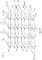
- FIGs. 1A and 1B are electrical schematic diagrams of a block 100 of memory cells according to various embodiments of the invention.
- the block 100 includes strings 110 of charge storage devices 118.
- a single NAND memory device may include multiple strings.
- the strings 110 are arranged in rows and columns in the block 100.
- FIG. 1A shows a single row of four strings 110 aligned with one vertical plane of the block 100 of memory cells.
- FIG. 1B shows three rows each having four strings 110 (for a total of twelve strings 110).
- Each string 110 includes four charge storage devices 118 coupled serially, although each string 110 may include fewer or more charge storage devices 118.
- Each string 110 includes a source select device 122 at a bottom of the string 110 and a drain select device 126 at a top of the string 110.
- the drain select device 126 is coupled between the charge storage devices 118 and a data line 130. There are four data lines 130 that are coupled to the strings 110, each data line 130 being coupled to three of the strings 110 in a column of the block 100.
- the source select device 122 is coupled between the charge storage devices 118 and a source gate 140.
- the source select device 122 has a source select gate (SGS) coupled to a SGS line 150.
- SGS source select gate
- the SGS lines 150 are substantially orthogonal to the data lines 130.
- the drain select device 126 has a drain select gate (SGD) coupled to a SGD line 160.
- SGD lines 160 are substantially orthogonal to the data lines 130.
- the source gate 140 substantially controls conduction in a first channel in the string 110 represented by a first source gate device 170 and a second channel in a substrate (not shown) represented by a second source gate device 172.
- the source gates 140 of all of the strings 110 in the block 100 are coupled to a single source gate line 176.
- the second source gate devices 172 in each row of the block 100 are coupled in series between the respective strings 110 and a common source line 180.
- Each of the charge storage devices 118 may comprise a transistor having a charge trap or a floating gate, for example.
- Each charge storage device 118 may comprise a multi-state device capable of holding multiple separate and distinct threshold oltage states(e.g., corresponding to respective ranges of threshold voltages), each threshold voltage state representing different data
- Each of the source select device 122 and the drain select device 126 may comprise a transistor.
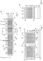
- FIG. 2 is a top view of a semiconductor construction 200 according to various embodiments of the invention.
- the semiconductor construction 200 includes three-hundred and sixty pillars 204 comprising a semiconductor material.
- the pillars 204 may comprise polysilicon.
- Each of the pillars 204 provides a channel for multiple charge storage devices in a string in a NAND memory device.
- the pillars 204 are arranged into eight rows of forty five columns with each pillar 204 occupying an intersection of a row and a column.
- the pillars 204 are divided into five blocks 210, 212, 214, 216 and 218 separated from each other by either empty space 220 or a conductive member (e.g., a conductive slot) 224 coupled to an n+ type diffusion region 228.
- the empty space 220 and space around the members 224 are filled with a dielectric (not shown) such as, for example, silicon dioxide (SiO 2 ).
- Each of the blocks 210, 212, 214, 216 and 218 includes seventy two of the pillars 204 in eight rows of nine columns.
- the pillars 204 in each row across all of the blocks 210, 212, 214, 216 and 218 are coupled together by a data line 232 or 233 that may be used to sense a state of one of the charge storage devices in the row.
- the data lines 232 and 233 may comprise, for example, polysilicon or metal, including one or more of cobalt (Co), titanium (Ti), tungsten (W), nickel (Ni) or tantalum (Ta) according to various embodiments of the invention.
- the semiconductor construction 200 can include different numbers of pillars 204 arranged in different numbers of rows and columns in different numbers of blocks according to various embodiments of the invention.
- FIG. 3 is a cross-sectional view of the semiconductor construction 200 along line 3-3 according to various embodiments of the invention and FIG. 4 is a cross-sectional view of the semiconductor construction 200 along line 4-4 according to various embodiments of the invention.
- FIG. 3 illustrates the pillars 204 in blocks 210 and 212 and one of the members 224 between the blocks 210 and 212.
- FIG. 4 illustrates the pillars 204 in the block 216.
- the pillars 204 extend from the data lines 232 and 233 to a p-type silicon well 310.
- the silicon well 310 is formed in an n-type silicon well 312 which is formed in a p-type silicon substrate 316.
- the n+ type diffusion region 228 is formed in the silicon well 310 and can reduce resistance to current How in the silicon well 310.
- a number of tiers of metal or semiconductor material surround or partially surround the pillars 204 between the data lines 232 and 233 and the silicon well 310 in each of the blocks 210, 212, 214, 216 and 218.
- the tiers are separated from each other by a dielectric (not shown) such as, for example, silicon dioxide (SiO 2 ).
- a majority of the tiers are access lines 320 and 322 to control the charge storage devices that receive and release charge through the pillars 204.
- Each of the access lines 320 and 322 surrounds or partially surrounds all of the pillars 204 in a block such as the blocks 210 and 212 shown in FIG. 3 .
- a tier between the access lines 320 and 322 and the data lines 232 and 233 is divided into drain select gates (SGDs) 330 and 360 that may substantially control conduction between the pillars 204 and the data lines 232 and 233.
- the eight pillars 204 in each column are surrounded or partially surrounded by a separate SGD 330 or 360.
- a tier below the access lines 320 and 322 is divided into source select gates (SGSs) 340 and 370 that may at least partially control conduction between the pillars 204 and the silicon well 310.
- the eight pillars 204 in each column are surrounded or partially surrounded by a separate SGS 340 or 370.
- a tier between the SGSs 340 and 370 and the silicon well 310 comprises a source gate 350.
- source gate 350 surrounds or partially surrounds all of the pillars 204 in a block such as the block 210 or the block 212 shown in FIG. 3 .
- the source gate 350 may at least partially control conduction between the pillars 204 and the silicon well 310.
- the members 224 each comprise a conductive structure, such as one having a wall shape, coupled to the n+ type diffusion region 228 in the silicon well 310, and that projects from the substrate 316.
- the members 224 comprise, for example, a semiconductor such as polysilicon or a metal such as tungsten.
- Each member 224 and the n+ type diffusion region 228 coupled to the member 224 can be used as a common source line in the semiconductor construction 200.
- the members 224 can be used to bias the silicon well 310 to a potential as desired.
- the members 224 can also reduce the resistance to current flow in the silicon well 310.
- the access lines 320 and 322, the SGDs 330 and 360, the SGSs 340 and 370 and the source gate 350 can be separated from each other by a dielectric such as, for example, silicon dioxide (SiO 2 ).
- the access lines 320 and 322, the SGDs 330 and 360, the SGSs 340 and 370 and the source gate 350 may comprise tiers of a semiconductor material such as silicon or polysilicon or polysilicon doped with Phosphorous or Boron.
- the access lines 320 and 322, the SGDs 330 and 360, the SGSs 340 and 370 and the source gate 350 may also comprise metal including one or more of Cobalt (Co), Titanium (Ti), Tungsten (W), Nickel (Ni) or Tantalum (Ta) according to various embodiments of the invention.
- the access lines 320 and 322 control charge storage devices surrounding or partially surrounding each pillar 204.
- Each charge storage device may comprise, for example, a floating gate transistor or a charge trap transistor.
- the SGDs 330 and 360, the SGSs 340 and 370 and the source gate 350 control transistors surrounding or partially surrounding each pillar 204.
- the selected charge storage device is read when the voltages shown in Table 1 are applied to the semiconductor construction 200.
- Table 1 Block 212 Block 210 Data line 233 ⁇ 0.3V ⁇ 0.3V Data lines 232 ⁇ OV ⁇ 0V Access line 322 0 to ⁇ 3V ⁇ 0V Access lines 320 ⁇ 6V ⁇ 0V SCID 360 ⁇ 4V N/A SGDs 330 ⁇ 0V ⁇ 0V SGS 370 ⁇ 4V N/A SGSs 340 ⁇ 0V ⁇ 0V Source gate 350 ⁇ 5V ⁇ 0V Member 224 ⁇ 0V ⁇ 0V Silicon Well 310 ⁇ 0V ⁇ 0V
- Approximately 4 volts is applied to turn on the SGD 360 and the SGS 370 and approximately 5 volts is applied to turn on the source gate 350 in the block 212 to couple the selected pillar 204 to the data, line 233 and the silicon well 310.
- a channel develops in the silicon well 310 under the block 212 due to the potential of the source gate 350 to carry charge from the block 212 to the member 224 and the n+ type diffusion region 228 coupled to the member 224 that can be a common source line.
- the access line 322 in the block 212 is coupled to between approximately 0 volts and approximately 3 volts in stages to gradually turn on the selected charge storage device, which can be in one of a plurality of charge storage states.
- the other SGDs 330 and SGSs 340 in the block 212 are coupled to approximately 0 volts and are not conductive, such that the channel does not receive charge from the pillars 204 other than the selected pillar 204.
- the data line 233 is precharged to approximately 0.3 volts to allow the selected charge storage device to be read, and the other data lines 232 are at approximately 0 volts.
- the access lines 320, the SGDs 330, the SGSs 340 and the source gate 350 in the block 210 are at approximately 0 volts.
- the data lines 232 and 233 and the silicon well 310 are at the same potential for the blocks 210 and 212.
- Charge storage devices associated with pillars other than the selected pillar 204 can be influenced during a read by the access lines 320 at approximately 6 volts, and may be programmed unintentionally. This unintentional programming is called read disturb.
- the inventors have discovered that the challenge noted above, as well as others, can be addressed by turning on the source gate 350 at 5 volts to allow the SGSs 340 of the pillars other than the selected pillar 204 to be turned off to substantially electrically isolate the pillars other than the selected pillar 204 from the silicon well 310.
- the SGSs 340 that are not conductive substantially prevent conduction between the pillars other than the selected pillar 204 and the silicon well 310 to substantially prevent read disturb activity with respect to those pillars 204.
- the selected charge storage device is programmed when the voltages shown in Table 2 are applied to the semiconductor construction 200.
- Table 2 Block 212 Block 210 Data line 233 0 to ⁇ 1V 0 to ⁇ 1V Data lines 232 ⁇ 2.3V ⁇ 2.3V Access line 322 ⁇ 20V ⁇ 0V Access lines 320 ⁇ 10V ⁇ 0V SGD 360 ⁇ 3V N/A S GDs 330 ⁇ 0V ⁇ 0V SGS 370 0 to ⁇ 3V N/A SGSs 340 0 to ⁇ 3V ⁇ 0V Source gate 350 ⁇ 0V ⁇ 0V Member 224 0 to ⁇ 2V 0 to ⁇ 2V Silicon Well 310 ⁇ 0V ⁇ 0V
- the SGSs 340 and 370 in the block 212 are biased to between approximately 0 and approximately 3 volts and the member 224 is biased to between approximately 0 and approximately 2 volts.
- the SGDs 330 and the source gate 350 in the block 212 and the silicon well 310 are biased to approximately 0 volts.
- Approximately 20 volts are applied to the access line 322 in the block 212 to turn on the selected charge storage device to program it.
- Approximately 10 volts are applied to the other access lines 320 in the block 212 to render the other charge storage devices associated with the selected pillar 204 conductive.
- the SGDs 330 that are biased to approximately 0 volts are not conductive such that the pillars in the block 212 other than the selected pillar 204 are floating and have a potential that rises to approximately 8 volts due to the potential on the access lines 320 of approximately 10 volts to substantially prevent programming.
- the data line 233 coupled to the selected pillar 204 is between approximately 0 and approximately 1 volt to allow the selected charge storage device to be programmed and the other data lines 232 are biased to approximately 2.3 volts.
- the access lines 320, the SGDs 330, the SGSs 340 and the source gate 350 in the block 210 are at approximately 0 volts.
- the data lines 232 and 233 and the silicon well 310 are at the same potential for the blocks 210 and 212.
- the source gate 350 is switched off to substantially reduce leakage of current to the n+ type diffusion region 228 and the member 224 and this can reduce program disturb activity during programming operations.
- the voltage applied to the SGSs 340 and 370 can be higher than the approximately 3 volts to reduce an electromagnetic field between the SGSs 340 and 370 and the access lines 320 and 322.
- the selected charge storage device is erased when the voltages shown in Table 3 are applied to the semiconductor construction 200.
- Table3 Block 212 Block 210 Data lines 232, 233 ⁇ 20V ⁇ 20V Access lines 320, 322 ⁇ 0V ⁇ 20V SGDs 330, 360 ⁇ 20V ⁇ 20V SGSs 340, 370 ⁇ 20V ⁇ 20V Source gate 350 ⁇ 20V ⁇ 20V Member 224 ⁇ 20V ⁇ 20V Silicon Well 310 ⁇ 20V ⁇ 20V
- Approximately 20 volts is applied to the silicon well 310 such that the potential on the pillars 204 rises to approximately 20 volts.
- the SGSs 340 and 370, the member 224, the source gate 350, the SGDs 330 and 360 and the data lines 232 and 233 are left floating and rise to approximately 20 volts from capacitive coupling with the pillars 204.
- Approximately 0 volts are applied to the access lines 320 and 322 in the block 212 to erase the charge storage devices associated with the pillar 204 above the SGS 370.
- the access lines 320 in the block 210 are also left floating and rise to approximately 20 volts from capacitive coupling with the pillars 204.
- FIG. 5 is a top view of a semiconductor construction 500 according to various embodiments of the invention.
- the semiconductor construction 500 includes two-hundred and fifty-six pillars 504 comprising a semiconductor material.
- the pillars 504 may comprise polysilicon.
- Each of the pillars 504 provides a channel for multiple charge storage devices in a string in a NAND memory device.
- the pillars 504 are divided into four blocks 510, 512, 514 and 516 separated from each other by a conductive member 524 coupled to an n+ type diffusion region 528.
- Each of the blocks 510, 512, 514 and 516 includes 64 of the pillars 504 separated into sub-blocks 529, each sub-block 529 including 16 of the pillars 504.
- Each sub-block 529 is separated from neighboring sub-blocks 529 in the same block by an n+ type diffusion region 530.
- Sixteen data lines 532 and 533 are coupled to tops of the pillars 504, and the pillars 504 are arranged in two staggered columns in each sub-block 529.
- the columns of the pillars 504 are substantially perpendicular to the data lines 532 and 533 such that each data line 532 and 533 is coupled to a top of only one of the pillars 504 in each sub-block 529 of the semiconductor construction 500.
- Each data line 532 and 533 may be used to sense a state of one of the charge storage devices in one of the sub-blocks 529.
- the data lines 532 and 533 may comprise, for example, polysilicon or metal, including one or more of cobalt (Co), titanium (Ti), tungsten (W), nickel (Ni) or tantalum (Ta), according to various embodiments of the invention.
- FIG. 6 is a cross-sectional view of the semiconductor construction 500 along line 6-6 according to various embodiments of the invention and FIG. 7 is a cross-sectional view of the semiconductor construction 500 along line 7-7 according to various embodiments of the invention.
- FIG. 6 shows the pillars 504 in the blocks 510 and 512 and one of the members 524 between the blocks 510 and 512.
- Half of the pillars 504 in the blocks 510 and 512 are shown in cross-section and half of the pillars 504 in the blocks 510 and 512 are not shown in cross-section but are staggered and behind the pillars 504 shown in cross-section.
- FIG. 7 shows eight of the pillars 504 and half of the data lines 532 and 533 in block 514 for purposes of brevity and clarity.
- the pillars 504 extend from the data lines 532 and 533 to a p-type silicon well 610.
- the silicon well 610 is formed in an n-type silicon well 612 which is formed in a p-type silicon substrate 616.
- the n+ type diffusion regions 528 and 530 are formed in the silicon well 610 and can reduce resistance to current flow in the silicon well 610.
- a number of tiers of metal or semiconductor material surround or partially surround the pillars 504 between the data lines 532 and 533 and the silicon well 610 in each of the blocks 510, 512, 514 and 516.
- the tiers are separated from each other by a dielectric (not shown) such as, for example, silicon dioxide (SiO 2 ).
- a majority of the tiers comprise access lines 620 and 622 to control the charge storage devices that receive and release charge through the pillars 504. All of the pillars 504 in a sub-block 529 are surrounded or partially surrounded by respective access lines 620 or 622.
- a tier between the access lines 620 and 622 and the data lines 532 and 533 is divided into SGDs 630 and 660 that may substantially control conduction between the pillars 504 and the data lines 532 and 533.
- the pillars 504 in each sub-block 529 are surrounded or partially surrounded by a separate SGD 630 or 660.
- a tier below the access lines 620 and 622 is divided into SGSs 640 and 670 that may at least partially control conduction between the pillars 504 and the silicon well 610.
- the pillars 504 in each sub-block 529 are surrounded or partially surrounded by a separate SGS 640 or 670.
- a tier between the SGSs 640 and 670 and the silicon well 610 is a source gate 650.
- the pillars 504 in each sub-block 529 are surrounded or partially surrounded by a separate source gate 650.
- the source gates 650 may also at least partially control conduction between the pillars 504 and the
- the members 524 each comprise a conductive structure, such as one having a wall shape, coupled to the n+ type diffusion region 528 in the silicon well 610, and that projects from the substrate 616.
- the members 524 comprise, for example, a semiconductor such as polysilicon or a metal such as tungsten.
- Each member 524 and the n+ type diffusion region 528 coupled to the member 524 can be used as a common source line in the semiconductor construction 500.
- the members 524 can be used to bias the silicon well 610 to a potential as desired.
- the members 524 can also reduce the resistance to current flow in the silicon well 610.
- the access lines 620 and 622, the SGDs 630 and 660, the SGSs 640 and 670 and the source gate 650 can be separated from each other by a dielectric such as, for example, silicon dioxide (SiO 2 ).
- the access lines 620 and 622, the SGDs 630 and 660, the SGSs 640 and 670 and the source gate 650 may comprise tiers of a semiconductor material such as silicon or polysilicon or polysilicon doped with Phosphorous or Boron.
- the access lines 620 and 622, the SGDs 630 and 660, the SGSs 640 and 670 and the source gate 650 may also comprise metal including one or more of cobalt (Co), titanium (Ti), tungsten (W), nickel (Ni) or tantalum (Ta) according to various embodiments of the invention.
- the access lines 620 and 622 control charge storage devices associated with each pillar 504.
- the SGDs 630 and 660, the SGSs 640 and 670 and the source gate 650 control transistors surrounding or partially surrounding each pillar 504.
- Each charge storage device may comprise, for example, a floating gate transistor or a charge trap transistor.
- the selected charge storage device is read when the voltages shown in Table 4 are applied to the semiconductor construction 500.
- Table 4 Block 512 Block 510 Data line 533 ⁇ 0.3V ⁇ 0.3V Data lines 532 ⁇ 0V ⁇ 0V Access line 622 0 to ⁇ 3V ⁇ 0V Access lines 620 ⁇ 6V ⁇ 0V SGD 660 ⁇ 4V ⁇ 0V SGDs 630 ⁇ 0V ⁇ 0V SGS 670 ⁇ 4V ⁇ 0V SGSs 640 ⁇ 0V ⁇ 0V Source gate 650 ⁇ 5V ⁇ 0V Member 524 ⁇ 0V ⁇ 0V Silicon Well 610 ⁇ 0V ⁇ 0V
- Approximately 4 volts is applied to turn on the SGD 660 and the SGS 670 and approximately 5 volts is applied to turn on the source gates 650 in the block 512 to couple the selected pillar 504 to the data line 533 and the silicon well 610.
- a channel develops in the silicon well 610 under the block 512 due to the potential of the source gate 650 to carry charge from the block 512 to the member 524 and the n+ type diffusion region 528 coupled to the member 524 that can be a common source line.
- the access line 622 in the block 512 is biased to a potential from approximately 0 to approximately 3 volts in stages to gradually turn on the selected charge storage device, which can be in one of a plurality of charge storage states.
- Approximately 6 volts are applied to the other access lines 620 in the block 512 and render the other charge storage devices associated with the selected pillar 504 conductive.
- the other SGDs 630 and SGSs 640 in the block 512 are biased to approximately 0 volts and are not conductive such that the channel does not receive charge from the pillars 504 other than the selected pillar 504.
- the data line 533 is precharged to approximately 0.3 volts to allow the selected charge storage device to be read, and the other data lines 532 are at approximately 0 volts.
- the access lines 620, the SGDs 630, the SGSs 640 and the source gate 650 in the block 510 are at approximately 0 volts.
- the data lines 532 and 533 and the silicon well 610 are at the same potential for the blocks 510 and 512.
- the pillar 504 that is between the SGD 660 and the SGS 670 that is not selected is not selected because it's coupled to one of the data lines 532 at approximately 0V.
- the source gates 650 in the block 512 are turned on at 5 volts to allow the SGSs 640 of the pillars other than the selected pillar 504 to be turned off to substantially electrically isolate the pillars other than the selected pillar 504 from the silicon well 610.
- the SGSs 640 that are not conductive substantially prevent conduction between the pillars other than the selected pillar 504 and the silicon well 610 to substantially prevent read disturb in those pillars.
- the selected charge storage device is programmed when the voltages shown in Table 5 are applied to the semiconductor construction 500.
- Table 5 Block 5 12 Block 510 Data line 533 0 to ⁇ 1V 0 to ⁇ 1V Data lines 532 ⁇ 2.3V ⁇ 2.3V Access line 622 ⁇ 20V ⁇ 0V Access lines 620 ⁇ 10V ⁇ 0V SGD 660 ⁇ 3V N/A SGDs 630 ⁇ 0V ⁇ 0V SGS 670 0 to ⁇ 3V N/A SGSs 640 0 to ⁇ 3V ⁇ 0V Source gate 650 ⁇ 0V ⁇ 0V Member 524 0 to ⁇ 2V 0 to ⁇ 2V Silicon Well 610 ⁇ 0V ⁇ 0V
- Approximately 3 volts is applied to turn on the SGD 660 in the block 512.
- the SGSs 640 and 670 in the block 512 are biased to between approximately 0 and approximately 3 volts and the member 524 is biased to between 0 and approximately 2 volts.
- the SGDs 630 and the source gate 650 in the block 512 and the silicon well 610 are biased to approximately 0 volts.
- Approximately 20 volts are applied to the access line 622 in the block 512 to turn on the selected charge storage device to program it.
- Approximately 10 volts are applied to the other access lines 620 in the block 512 and render the other charge storage devices associated with the selected pillar 504 conductive.
- the SGDs 630 in the block 512 that are biased to approximately 0 volts are not conductive, such that the pillars other than the selected pillar 504 are floating and have a potential that rises to approximately 8 volts due to the potential on the access lines 620 of approximately 10 volts to substantially prevent programming.
- the data line 533 coupled to the selected pillar 504 is between approximately 0 volts and approximately 1 volt to allow the selected charge storage device to be programmed and the other data lines 532 are biased to approximately 2.3 volts.
- the access lines 620, the SGDs 630, the SGSs 640 and the source gate 650 in the block 510 are at approximately 0 volts.
- the data lines 532 and 533 and the silicon well 610 are at the same potential for the blocks 510 and 512.
- the source gate 650 in the block 512 is switched off to substantially reduce leakage of current to the n+ type diffusion region 528 and the member 524 and this can reduce program disturb activity during the programming.
- the voltage applied to the SGSs 640 and 670 can be higher than the approximately 3 volts, such as to reduce an electromagnetic field between the SGSs 640 and 670 and the access lines 620 and 622.
- the selected charge storage device is erased when the voltages shown in Table 6 are applied to the semiconductor construction 500.
- Table 6 Block 512 Block 510 Data lines 532, 533 ⁇ 20V ⁇ 20V Access lines 620, 622 ⁇ 0V ⁇ 20V SGDs 630,660 ⁇ 20V ⁇ 20V SGSs 640, 670 ⁇ 20V ⁇ 20V Source gate 650 ⁇ 20V ⁇ 20V Member 524 ⁇ 20V ⁇ 20V Silicon Well 610 ⁇ 20V ⁇ 20V
- Approximately 20 volts is applied to the silicon well 610 such that the potential on the pillars 504 rises to approximately 20 volts.
- the SGSs 640 and 670, the member 524, the source gate 650, the SGDs 630 and 660 and the data lines 532 and 533 are left floating and rise to approximately 20 volts from capacitive coupling with the pillars 504.
- Approximately 0 volts are applied to the access lines 620 and 622 in the block 512 to erase the charge storage devices associated with the pillar 504 above the SGS 670.
- the access lines 620 in the block 510 are left floating and rise to approximately 20 volts from capacitive coupling with the pillars 504.
- FIG. 8 is a cross-sectional view of the semiconductor construction 200 along line 8-8 according to various embodiments of the invention.
- FIG. 8 illustrates four of the pillars 204 in the block 218 extending from the data line 233 to the p-type silicon well 310 and the tiers including the access lines 320 and 322, the SGDs 330, the SGSs 340 and the source gate 350. Silicon dioxide 810 is formed at edges of the SGDs 330.
- FIG. 8 illustrates charge storage devices 820 between the access lines 320 and 322 and the pillars 204.
- Each charge storage device 820 includes a polysilicon storage layer 830 separated from one of the pillars 204 by a tunnel dielectric 840 that can be silicon dioxide.
- the charge storage layer 830 is separated from the access line 320 or 322 by a blocking dielectric 850 that can include silicon dioxide, silicon nitride (Si 3 N 4 ) and silicon dioxide (ONO).
- FIG. 9 is a flow diagram of a method 900 according to various embodiments of the invention.
- the method 900 starts.
- strings are coupled to data lines.
- the strings are coupled to a substrate.
- some of the strings are substantially electrically isolated from the substrate.
- the method 900 ends.
- Various embodiments may have more or fewer activities than those shown in FIG. 9 . In some embodiments, the activities may be repeated, and/or performed in serial or parallel fashion. Some embodiments may comprise the same activities in a different order.
- FIG. 10 is a diagram illustrating a system 1000 according to various embodiments of the invention.
- the system 1000 may include a processor 1010, a memory device 1020, a memory controller 1030, a graphic controller 1040, an input and output (I/O) controller 1050, a display 1052, a keyboard 1054, a pointing device 1056, and a peripheral device 1058.
- a bus 1060 couples all of these devices together.
- a clock generator 1070 is coupled to the bus 1060 to provide a clock signal to at least one of the devices of the system 1000 through the bus 1060.
- the clock generator 1070 may include an oscillator in a circuit board such as a motherboard. Two or more devices shown in system 1000 may be formed in a single integrated circuit chip.
- the memory device 1020 may comprise one or more of the block 100 of memory cells described herein and shown in the figures (e.g., see FIGs. 1A and 1B ) according to various embodiments of the invention.
- the memory device 1020 may comprise one or more of the semiconductor constructions 200, 500 and 800 described herein and shown in the figures according to various embodiments of the invention.
- the bus 1060 may be interconnect traces on a circuit board or may be one or more cables.
- the bus 1060 may couple the devices of the system 1000 by wireless means such as by electromagnetic radiations, for example, radio waves.
- the peripheral device 1058 coupled to the I/O controller 1050 may be a printer, an optical device such as a CD-ROM and a DVD reader and writer, a magnetic device reader and writer such as a floppy disk driver, or an audio device such as a microphone.
- the system 1000 represented by FIG. 10 may include computers (e.g., desktops, laptops, hand-helds, servers, Web appliances, routers, etc.), wireless communication devices (e.g., cellular phones, cordless phones, pagers, personal digital assistants, etc.), computer-related peripherals (e.g., printers, scanners, monitors, etc.), entertainment devices (e.g., televisions, radios, stereos, tape and compact disc players, video cassette recorders, camcorders, digital cameras, MP3 (Motion Picture Experts Group, Audio Layer 3) players, video games, watches, etc.), and the like.
- computers e.g., desktops, laptops, hand-helds, servers, Web appliances, routers, etc.
- wireless communication devices e.g., cellular phones, cordless phones, pagers, personal digital assistants, etc.
- computer-related peripherals e.g., printers, scanners, monitors, etc.
- entertainment devices e.g., televisions, radios
- Charge storage devices in NAND memory devices can be subject to read disturb stress during read operations.
- the inventors have discovered that the challenges noted above, as well as others, can be addressed with, for example, a source gate device coupled to strings between one or more source select devices and a well in a substrate.
- Read disturb stress can be substantially reduced by turning off the source select devices in deselected strings during a read operation to substantially electrically isolate the deselected strings from the well in the substrate to substantially prevent conduction between the deselected strings and the well.
- a conductive member coupled to the substrate can reduce resistance to current flow in the well in the substrate.
Description
- Semiconductor memory devices are used in many electronic devices such as personal digital assistants (PDAs), laptop computers, mobile phones and digital cameras. Some of these semiconductor memory devices have arrays of charge storage transistors.
-
US2010/238732A andUS2011/194357A disclose apparatus comprising: a string of charge storage devices associated with a pillar comprising semiconductor material; a source gate device; and a source select device coupled between the string of charge storage devices and the source gate device. - The invention is in the apparatus of claim 1.
- Some embodiments are illustrated by way of example and not limitation in the figures of the accompanying drawings in which:
-
FIGs. 1A and1B are electrical schematic diagrams of a block of memory cells according to various embodiments of the invention; -
FIG. 2 is a top view of a semiconductor construction according to various embodiments of the invention; -
FIG. 3 is a cross-sectional view of a semiconductor construction according to various embodiments of the invention; -
FIG. 4 is a cross-sectional view of a semiconductor construction according to various embodiments of the invention; -
FIG. 5 is a top view of a semiconductor construction according to various embodiments of the invention; -
FIG. 6 is a cross-sectional view of a semiconductor construction according to various embodiments of the invention; -
FIG. 7 is a cross-sectional view of a semiconductor construction according to various embodiments of the invention; -
FIG. 8 is a cross-sectional view of a semiconductor construction according to various embodiments of the invention; -
FIG. 9 is a flow diagram of a method according to various embodiments of the invention; and -
FIG. 10 is a diagram illustrating a system according to various embodiments of the invention. - An array of charge storage devices according to various embodiments of the invention may function as an array of memory cells in a memory device such as a NOT AND (NAND) memory device.
- For the purposes of this document, a "tier of semiconductor material" can mean semiconductor material formed in a same plane, rank, row, or unit, such as in a horizontal or vertical or sloped plane, row, rank or unit of a structure. Meanwhile, an "apparatus" can refer to circuitry, devices or systems.
-
FIGs. 1A and1B are electrical schematic diagrams of ablock 100 of memory cells according to various embodiments of the invention. Theblock 100 includesstrings 110 ofcharge storage devices 118. A single NAND memory device may include multiple strings. - The
strings 110 are arranged in rows and columns in theblock 100.FIG. 1A shows a single row of fourstrings 110 aligned with one vertical plane of theblock 100 of memory cells.FIG. 1B shows three rows each having four strings 110 (for a total of twelve strings 110). Eachstring 110 includes fourcharge storage devices 118 coupled serially, although eachstring 110 may include fewer or morecharge storage devices 118. Eachstring 110 includes a sourceselect device 122 at a bottom of thestring 110 and a drainselect device 126 at a top of thestring 110. - The drain
select device 126 is coupled between thecharge storage devices 118 and adata line 130. There are fourdata lines 130 that are coupled to thestrings 110, eachdata line 130 being coupled to three of thestrings 110 in a column of theblock 100. The sourceselect device 122 is coupled between thecharge storage devices 118 and asource gate 140. - The source
select device 122 has a source select gate (SGS) coupled to aSGS line 150. There are threeSGS lines 150 that are coupled to the sourceselect devices 122 in theblock 100, eachSGS line 150 being coupled to gates of four of the sourceselect devices 122 in a row of theblock 100. TheSGS lines 150 are substantially orthogonal to thedata lines 130. - The drain
select device 126 has a drain select gate (SGD) coupled to aSGD line 160. There are threeSGD lines 160 that are coupled to the drainselect devices 126 in theblock 100, eachSGD line 160 being coupled to gates of four of the drainselect devices 126 in a row of theblock 100. TheSGD lines 160 are substantially orthogonal to thedata lines 130. Thesource gate 140 substantially controls conduction in a first channel in thestring 110 represented by a firstsource gate device 170 and a second channel in a substrate (not shown) represented by a secondsource gate device 172. Thesource gates 140 of all of thestrings 110 in theblock 100 are coupled to a singlesource gate line 176. The secondsource gate devices 172 in each row of theblock 100 are coupled in series between therespective strings 110 and acommon source line 180. - Each of the
charge storage devices 118 may comprise a transistor having a charge trap or a floating gate, for example. Eachcharge storage device 118 may comprise a multi-state device capable of holding multiple separate and distinct threshold oltage states(e.g., corresponding to respective ranges of threshold voltages), each threshold voltage state representing different data Each of the sourceselect device 122 and the drainselect device 126 may comprise a transistor. -
FIG. 2 is a top view of asemiconductor construction 200 according to various embodiments of the invention. Thesemiconductor construction 200 includes three-hundred and sixtypillars 204 comprising a semiconductor material. For example, thepillars 204 may comprise polysilicon. Each of thepillars 204 provides a channel for multiple charge storage devices in a string in a NAND memory device. - The
pillars 204 are arranged into eight rows of forty five columns with eachpillar 204 occupying an intersection of a row and a column. Thepillars 204 are divided into fiveblocks empty space 220 or a conductive member (e.g., a conductive slot) 224 coupled to an n+type diffusion region 228. Theempty space 220 and space around themembers 224 are filled with a dielectric (not shown) such as, for example, silicon dioxide (SiO2). Each of theblocks pillars 204 in eight rows of nine columns. Thepillars 204 in each row across all of theblocks data line data lines semiconductor construction 200 can include different numbers ofpillars 204 arranged in different numbers of rows and columns in different numbers of blocks according to various embodiments of the invention. -
FIG. 3 is a cross-sectional view of thesemiconductor construction 200 along line 3-3 according to various embodiments of the invention andFIG. 4 is a cross-sectional view of thesemiconductor construction 200 along line 4-4 according to various embodiments of the invention.FIG. 3 illustrates thepillars 204 inblocks members 224 between theblocks FIG. 4 illustrates thepillars 204 in theblock 216. - The
pillars 204 extend from thedata lines silicon well 310 is formed in an n-type silicon well 312 which is formed in a p-type silicon substrate 316. The n+type diffusion region 228 is formed in the silicon well 310 and can reduce resistance to current How in the silicon well 310. A number of tiers of metal or semiconductor material surround or partially surround thepillars 204 between thedata lines blocks access lines pillars 204. Each of theaccess lines pillars 204 in a block such as theblocks FIG. 3 . - A tier between the
access lines data lines pillars 204 and thedata lines pillars 204 in each column are surrounded or partially surrounded by aseparate SGD access lines pillars 204 and thesilicon well 310. The eightpillars 204 in each column are surrounded or partially surrounded by aseparate SGS - A tier between the
SGSs source gate 350. In the embodiment depicted inFIGS. 2-4 ,source gate 350 surrounds or partially surrounds all of thepillars 204 in a block such as theblock 210 or theblock 212 shown inFIG. 3 . Thesource gate 350 may at least partially control conduction between thepillars 204 and thesilicon well 310. - The
members 224 each comprise a conductive structure, such as one having a wall shape, coupled to the n+type diffusion region 228 in the silicon well 310, and that projects from thesubstrate 316. Themembers 224 comprise, for example, a semiconductor such as polysilicon or a metal such as tungsten. Eachmember 224 and the n+type diffusion region 228 coupled to themember 224 can be used as a common source line in thesemiconductor construction 200. Themembers 224 can be used to bias the silicon well 310 to a potential as desired. Themembers 224 can also reduce the resistance to current flow in thesilicon well 310. - The access lines 320 and 322, the
SGDs SGSs source gate 350 can be separated from each other by a dielectric such as, for example, silicon dioxide (SiO2). The access lines 320 and 322, theSGDs SGSs source gate 350 may comprise tiers of a semiconductor material such as silicon or polysilicon or polysilicon doped with Phosphorous or Boron. The access lines 320 and 322, theSGDs SGSs source gate 350 may also comprise metal including one or more of Cobalt (Co), Titanium (Ti), Tungsten (W), Nickel (Ni) or Tantalum (Ta) according to various embodiments of the invention. - The access lines 320 and 322 control charge storage devices surrounding or partially surrounding each
pillar 204. Each charge storage device may comprise, for example, a floating gate transistor or a charge trap transistor. TheSGDs SGSs source gate 350 control transistors surrounding or partially surrounding eachpillar 204. - Operations involving charge storage devices in the
semiconductor construction 200 will be described with reference to a selected charge storage device having a channel in a selectedpillar 204 between theSGD 360 and theSGS 370 in theblock 212. The selectedpillar 204 is coupled to thedata line 233. The selected charge storage device is controlled by theaccess line 322. - The selected charge storage device is read when the voltages shown in Table 1 are applied to the
semiconductor construction 200.Table 1 Block 212Block 210Data line 233∼0.3V ∼0.3 V Data lines 232 ∼OV ∼ 0V Access line 322 0 to ∼3V ∼ 0V Access lines 320 ∼6V ∼ 0V SCID 360 ∼4V N/ A SGDs 330 ∼0V ∼ 0V SGS 370 ∼4V N/ A SGSs 340 ∼0V ∼ 0V Source gate 350 ∼5V ∼ 0V Member 224 ∼0V ∼ 0V Silicon Well 310 ∼0V ∼0V - Approximately 4 volts is applied to turn on the
SGD 360 and theSGS 370 and approximately 5 volts is applied to turn on thesource gate 350 in theblock 212 to couple the selectedpillar 204 to the data,line 233 and thesilicon well 310. A channel develops in the silicon well 310 under theblock 212 due to the potential of thesource gate 350 to carry charge from theblock 212 to themember 224 and the n+type diffusion region 228 coupled to themember 224 that can be a common source line. Theaccess line 322 in theblock 212 is coupled to between approximately 0 volts and approximately 3 volts in stages to gradually turn on the selected charge storage device, which can be in one of a plurality of charge storage states. Approximately 6 volts are applied to theother access lines 320 in theblock 212 to render the other charge storage devices associated with the selectedpillar 204 conductive. Theother SGDs 330 andSGSs 340 in theblock 212 are coupled to approximately 0 volts and are not conductive, such that the channel does not receive charge from thepillars 204 other than the selectedpillar 204. Thedata line 233 is precharged to approximately 0.3 volts to allow the selected charge storage device to be read, and theother data lines 232 are at approximately 0 volts. The access lines 320, theSGDs 330, theSGSs 340 and thesource gate 350 in theblock 210 are at approximately 0 volts. The data lines 232 and 233 and the silicon well 310 are at the same potential for theblocks - Charge storage devices associated with pillars other than the selected
pillar 204 can be influenced during a read by theaccess lines 320 at approximately 6 volts, and may be programmed unintentionally. This unintentional programming is called read disturb. The inventors have discovered that the challenge noted above, as well as others, can be addressed by turning on thesource gate 350 at 5 volts to allow theSGSs 340 of the pillars other than the selectedpillar 204 to be turned off to substantially electrically isolate the pillars other than the selectedpillar 204 from thesilicon well 310. TheSGSs 340 that are not conductive substantially prevent conduction between the pillars other than the selectedpillar 204 and the silicon well 310 to substantially prevent read disturb activity with respect to thosepillars 204. - The selected charge storage device is programmed when the voltages shown in Table 2 are applied to the
semiconductor construction 200.Table 2 Block 212Block 210Data line 2330 to ∼1V 0 to ∼ 1V Data lines 232 ∼2.3V ∼2.3 V Access line 322 ∼20V ∼ 0V Access lines 320 ∼10V ∼ 0V SGD 360 ∼3V N/ A S GDs 330 ∼0V ∼ 0V SGS 370 0 to ∼3V N/ A SGSs 340 0 to ∼3V ∼ 0V Source gate 350 ∼0V ∼ 0V Member 224 0 to ∼2V 0 to ∼ 2V Silicon Well 310 ∼0V ∼0V - Approximately 3 volts is applied to turn on the
SGD 360. TheSGSs block 212 are biased to between approximately 0 and approximately 3 volts and themember 224 is biased to between approximately 0 and approximately 2 volts. TheSGDs 330 and thesource gate 350 in theblock 212 and the silicon well 310 are biased to approximately 0 volts. Approximately 20 volts are applied to theaccess line 322 in theblock 212 to turn on the selected charge storage device to program it. Approximately 10 volts are applied to theother access lines 320 in theblock 212 to render the other charge storage devices associated with the selectedpillar 204 conductive. TheSGDs 330 that are biased to approximately 0 volts are not conductive such that the pillars in theblock 212 other than the selectedpillar 204 are floating and have a potential that rises to approximately 8 volts due to the potential on theaccess lines 320 of approximately 10 volts to substantially prevent programming. Thedata line 233 coupled to the selectedpillar 204 is between approximately 0 and approximately 1 volt to allow the selected charge storage device to be programmed and theother data lines 232 are biased to approximately 2.3 volts. The access lines 320, theSGDs 330, theSGSs 340 and thesource gate 350 in theblock 210 are at approximately 0 volts. The data lines 232 and 233 and the silicon well 310 are at the same potential for theblocks - The
source gate 350 is switched off to substantially reduce leakage of current to the n+type diffusion region 228 and themember 224 and this can reduce program disturb activity during programming operations. The voltage applied to theSGSs SGSs access lines - The selected charge storage device is erased when the voltages shown in Table 3 are applied to the
semiconductor construction 200.Table3 Block 212 Block 210Data lines ∼20V ∼ 20V Access lines 320, 322 ∼0V ∼20V SGDs 330, 360 ∼20V ∼20V SGSs 340, 370 ∼20V ∼ 20V Source gate 350 ∼20V ∼ 20V Member 224 ∼20V ∼ 20V Silicon Well 310 ∼20V ∼20V - Approximately 20 volts is applied to the silicon well 310 such that the potential on the
pillars 204 rises to approximately 20 volts. TheSGSs member 224, thesource gate 350, theSGDs data lines pillars 204. Approximately 0 volts are applied to theaccess lines block 212 to erase the charge storage devices associated with thepillar 204 above theSGS 370. The access lines 320 in theblock 210 are also left floating and rise to approximately 20 volts from capacitive coupling with thepillars 204. -
FIG. 5 is a top view of asemiconductor construction 500 according to various embodiments of the invention. Thesemiconductor construction 500 includes two-hundred and fifty-sixpillars 504 comprising a semiconductor material. For example, thepillars 504 may comprise polysilicon. Each of thepillars 504 provides a channel for multiple charge storage devices in a string in a NAND memory device. - The
pillars 504 are divided into fourblocks conductive member 524 coupled to an n+type diffusion region 528. Each of theblocks pillars 504 separated intosub-blocks 529, each sub-block 529 including 16 of thepillars 504. Each sub-block 529 is separated from neighboringsub-blocks 529 in the same block by an n+type diffusion region 530. Sixteendata lines pillars 504, and thepillars 504 are arranged in two staggered columns in each sub-block 529. The columns of thepillars 504 are substantially perpendicular to thedata lines data line pillars 504 in each sub-block 529 of thesemiconductor construction 500. Eachdata line -
FIG. 6 is a cross-sectional view of thesemiconductor construction 500 along line 6-6 according to various embodiments of the invention andFIG. 7 is a cross-sectional view of thesemiconductor construction 500 along line 7-7 according to various embodiments of the invention.FIG. 6 shows thepillars 504 in theblocks members 524 between theblocks pillars 504 in theblocks pillars 504 in theblocks pillars 504 shown in cross-section. Thepillars 504 that are staggered and behind thepillars 504 shown in cross-section are coupled to adata line 532 behind thedata line 533 shown inFIG. 6. FIG. 7 shows eight of thepillars 504 and half of thedata lines block 514 for purposes of brevity and clarity. - The
pillars 504 extend from thedata lines type silicon well 610. The silicon well 610 is formed in an n-type silicon well 612 which is formed in a p-type silicon substrate 616. The n+type diffusion regions silicon well 610. A number of tiers of metal or semiconductor material surround or partially surround thepillars 504 between thedata lines blocks access lines pillars 504. All of thepillars 504 in a sub-block 529 are surrounded or partially surrounded byrespective access lines - A tier between the
access lines data lines SGDs pillars 504 and thedata lines pillars 504 in each sub-block 529 are surrounded or partially surrounded by aseparate SGD access lines SGSs pillars 504 and thesilicon well 610. Thepillars 504 in each sub-block 529 are surrounded or partially surrounded by aseparate SGS SGSs source gate 650. Thepillars 504 in each sub-block 529 are surrounded or partially surrounded by aseparate source gate 650. Thesource gates 650 may also at least partially control conduction between thepillars 504 and thesilicon well 610. - The
members 524 each comprise a conductive structure, such as one having a wall shape, coupled to the n+type diffusion region 528 in the silicon well 610, and that projects from thesubstrate 616. Themembers 524 comprise, for example, a semiconductor such as polysilicon or a metal such as tungsten. Eachmember 524 and the n+type diffusion region 528 coupled to themember 524 can be used as a common source line in thesemiconductor construction 500. Themembers 524 can be used to bias the silicon well 610 to a potential as desired. Themembers 524 can also reduce the resistance to current flow in thesilicon well 610. - The access lines 620 and 622, the
SGDs SGSs source gate 650 can be separated from each other by a dielectric such as, for example, silicon dioxide (SiO2). The access lines 620 and 622, theSGDs SGSs source gate 650 may comprise tiers of a semiconductor material such as silicon or polysilicon or polysilicon doped with Phosphorous or Boron. The access lines 620 and 622, theSGDs SGSs source gate 650 may also comprise metal including one or more of cobalt (Co), titanium (Ti), tungsten (W), nickel (Ni) or tantalum (Ta) according to various embodiments of the invention. The access lines 620 and 622 control charge storage devices associated with eachpillar 504. TheSGDs SGSs source gate 650 control transistors surrounding or partially surrounding eachpillar 504. Each charge storage device may comprise, for example, a floating gate transistor or a charge trap transistor. - Operations involving charge storage devices in the
semiconductor construction 500 will be described with reference to a selected charge storage device having a channel in a selectedpillar 504 between theSGD 660 and theSGS 670 in theblock 512. The selectedpillar 504 is coupled to thedata line 533. The selected charge storage device is controlled by theaccess line 622. - The selected charge storage device is read when the voltages shown in Table 4 are applied to the
semiconductor construction 500.Table 4 Block 512Block 510Data line 533∼0.3V ∼0.3 V Data lines 532 ∼0V ∼ 0V Access line 622 0 to ∼3V ∼ 0V Access lines 620 ∼6V ∼ 0V SGD 660 ∼4V ∼ 0V SGDs 630 ∼0V ∼ 0V SGS 670 ∼4V ∼ 0V SGSs 640 ∼0V ∼ 0V Source gate 650 ∼5V ∼ 0V Member 524 ∼0V ∼ 0V Silicon Well 610 ∼0V ∼0V - Approximately 4 volts is applied to turn on the
SGD 660 and theSGS 670 and approximately 5 volts is applied to turn on thesource gates 650 in theblock 512 to couple the selectedpillar 504 to thedata line 533 and thesilicon well 610. A channel develops in the silicon well 610 under theblock 512 due to the potential of thesource gate 650 to carry charge from theblock 512 to themember 524 and the n+type diffusion region 528 coupled to themember 524 that can be a common source line. Theaccess line 622 in theblock 512 is biased to a potential from approximately 0 to approximately 3 volts in stages to gradually turn on the selected charge storage device, which can be in one of a plurality of charge storage states. Approximately 6 volts are applied to theother access lines 620 in theblock 512 and render the other charge storage devices associated with the selectedpillar 504 conductive. Theother SGDs 630 andSGSs 640 in theblock 512 are biased to approximately 0 volts and are not conductive such that the channel does not receive charge from thepillars 504 other than the selectedpillar 504. Thedata line 533 is precharged to approximately 0.3 volts to allow the selected charge storage device to be read, and theother data lines 532 are at approximately 0 volts. The access lines 620, theSGDs 630, theSGSs 640 and thesource gate 650 in theblock 510 are at approximately 0 volts. The data lines 532 and 533 and the silicon well 610 are at the same potential for theblocks pillar 504 that is between theSGD 660 and theSGS 670 that is not selected is not selected because it's coupled to one of thedata lines 532 at approximately 0V. - The
source gates 650 in theblock 512 are turned on at 5 volts to allow theSGSs 640 of the pillars other than the selectedpillar 504 to be turned off to substantially electrically isolate the pillars other than the selectedpillar 504 from thesilicon well 610. TheSGSs 640 that are not conductive substantially prevent conduction between the pillars other than the selectedpillar 504 and the silicon well 610 to substantially prevent read disturb in those pillars. - The selected charge storage device is programmed when the voltages shown in Table 5 are applied to the
semiconductor construction 500.Table 5 Block 5 12 Block 510Data line 5330 to ∼1V 0 to ∼ 1V Data lines 532 ∼2.3V ∼2.3 V Access line 622 ∼20V ∼ 0V Access lines 620 ∼10V ∼ 0V SGD 660 ∼3V N/ A SGDs 630 ∼0V ∼ 0V SGS 670 0 to ∼3V N/ A SGSs 640 0 to ∼3V ∼ 0V Source gate 650 ∼0V ∼ 0V Member 524 0 to ∼2V 0 to ∼ 2V Silicon Well 610 ∼0V ∼0V - Approximately 3 volts is applied to turn on the
SGD 660 in theblock 512. TheSGSs block 512 are biased to between approximately 0 and approximately 3 volts and themember 524 is biased to between 0 and approximately 2 volts. TheSGDs 630 and thesource gate 650 in theblock 512 and the silicon well 610 are biased to approximately 0 volts. Approximately 20 volts are applied to theaccess line 622 in theblock 512 to turn on the selected charge storage device to program it. Approximately 10 volts are applied to theother access lines 620 in theblock 512 and render the other charge storage devices associated with the selectedpillar 504 conductive. TheSGDs 630 in theblock 512 that are biased to approximately 0 volts are not conductive, such that the pillars other than the selectedpillar 504 are floating and have a potential that rises to approximately 8 volts due to the potential on theaccess lines 620 of approximately 10 volts to substantially prevent programming. Thedata line 533 coupled to the selectedpillar 504 is between approximately 0 volts and approximately 1 volt to allow the selected charge storage device to be programmed and theother data lines 532 are biased to approximately 2.3 volts. The access lines 620, theSGDs 630, theSGSs 640 and thesource gate 650 in theblock 510 are at approximately 0 volts. The data lines 532 and 533 and the silicon well 610 are at the same potential for theblocks - The
source gate 650 in theblock 512 is switched off to substantially reduce leakage of current to the n+type diffusion region 528 and themember 524 and this can reduce program disturb activity during the programming. The voltage applied to theSGSs SGSs access lines - The selected charge storage device is erased when the voltages shown in Table 6 are applied to the
semiconductor construction 500.Table 6 Block 512Block 510Data lines ∼20V ∼ 20V Access lines 620, 622 ∼0V ∼20V SGDs 630,660 ∼20V ∼ 20V SGSs 640, 670 ∼20V ∼ 20V Source gate 650 ∼20V ∼ 20V Member 524 ∼20V ∼ 20V Silicon Well 610 ∼20V ∼20V - Approximately 20 volts is applied to the silicon well 610 such that the potential on the
pillars 504 rises to approximately 20 volts. TheSGSs member 524, thesource gate 650, theSGDs data lines pillars 504. Approximately 0 volts are applied to theaccess lines block 512 to erase the charge storage devices associated with thepillar 504 above theSGS 670. The access lines 620 in theblock 510 are left floating and rise to approximately 20 volts from capacitive coupling with thepillars 504. -
FIG. 8 is a cross-sectional view of thesemiconductor construction 200 along line 8-8 according to various embodiments of the invention.FIG. 8 illustrates four of thepillars 204 in theblock 218 extending from thedata line 233 to the p-type silicon well 310 and the tiers including theaccess lines SGDs 330, theSGSs 340 and thesource gate 350.Silicon dioxide 810 is formed at edges of theSGDs 330.FIG. 8 illustratescharge storage devices 820 between theaccess lines pillars 204. Eachcharge storage device 820 includes apolysilicon storage layer 830 separated from one of thepillars 204 by atunnel dielectric 840 that can be silicon dioxide. Thecharge storage layer 830 is separated from theaccess line -
FIG. 9 is a flow diagram of amethod 900 according to various embodiments of the invention. Inblock 910, themethod 900 starts. Inblock 920, strings are coupled to data lines. Inblock 930, the strings are coupled to a substrate. Inblock 940, some of the strings are substantially electrically isolated from the substrate. Inblock 950, themethod 900 ends. Various embodiments may have more or fewer activities than those shown inFIG. 9 . In some embodiments, the activities may be repeated, and/or performed in serial or parallel fashion. Some embodiments may comprise the same activities in a different order. -
FIG. 10 is a diagram illustrating asystem 1000 according to various embodiments of the invention. Thesystem 1000 may include aprocessor 1010, amemory device 1020, amemory controller 1030, agraphic controller 1040, an input and output (I/O)controller 1050, adisplay 1052, akeyboard 1054, apointing device 1056, and aperipheral device 1058. Abus 1060 couples all of these devices together. Aclock generator 1070 is coupled to thebus 1060 to provide a clock signal to at least one of the devices of thesystem 1000 through thebus 1060. Theclock generator 1070 may include an oscillator in a circuit board such as a motherboard. Two or more devices shown insystem 1000 may be formed in a single integrated circuit chip. Thememory device 1020 may comprise one or more of theblock 100 of memory cells described herein and shown in the figures (e.g., seeFIGs. 1A and1B ) according to various embodiments of the invention. - The
memory device 1020 may comprise one or more of thesemiconductor constructions bus 1060 may be interconnect traces on a circuit board or may be one or more cables. Thebus 1060 may couple the devices of thesystem 1000 by wireless means such as by electromagnetic radiations, for example, radio waves. Theperipheral device 1058 coupled to the I/O controller 1050 may be a printer, an optical device such as a CD-ROM and a DVD reader and writer, a magnetic device reader and writer such as a floppy disk driver, or an audio device such as a microphone. - The
system 1000 represented byFIG. 10 may include computers (e.g., desktops, laptops, hand-helds, servers, Web appliances, routers, etc.), wireless communication devices (e.g., cellular phones, cordless phones, pagers, personal digital assistants, etc.), computer-related peripherals (e.g., printers, scanners, monitors, etc.), entertainment devices (e.g., televisions, radios, stereos, tape and compact disc players, video cassette recorders, camcorders, digital cameras, MP3 (Motion Picture Experts Group, Audio Layer 3) players, video games, watches, etc.), and the like. - Charge storage devices in NAND memory devices can be subject to read disturb stress during read operations. The inventors have discovered that the challenges noted above, as well as others, can be addressed with, for example, a source gate device coupled to strings between one or more source select devices and a well in a substrate. Read disturb stress can be substantially reduced by turning off the source select devices in deselected strings during a read operation to substantially electrically isolate the deselected strings from the well in the substrate to substantially prevent conduction between the deselected strings and the well. A conductive member coupled to the substrate can reduce resistance to current flow in the well in the substrate.
Claims (15)
- An apparatus comprising:a first string (110) of charge storage devices (118) associated with a first pillar (204) comprising semiconductor material; a second string (110) of charge storage devices (118) associated with a second pillar (204);each string including:a source gate device (170) having a gate (140), the source gate device coupled to a source (180); anda source select device (122) having a gate, the source select device (122) coupled between the charge storage devices (118) and the source gate device (170),wherein the gates (140) of the source gate devices (170) are coupled to each other to be controlled in common; andwherein the gates of the source select devices (122) are separate from one another to be controllable independently of one another.
- The apparatus of claim 1, comprising:multiple additional strings (110) of the charge storage devices (118), each string associated with a respective pillar (204) forming a channel of the string, the strings arranged in rows and columns,each additional string (110) including:a source gate device (170) coupled to a source (180) and configured to partially control conduction between the channel of charge storage devices (118) in the string (110) and a source (180), wherein a gate (140) of the source gate device (170) is coupled to the gate (140) of a source gate device (170) in another row of the memory unit, and also to the gate (140) of a source gate device (170) in another column of the memory unit; andthe source select device (122) coupled between the string of charge storage devices (110) and the source gate device (170), the source select device (122) configured to partially control conduction between the channel and the source (180).
- The apparatus of claim 1 or 2, wherein each string (110) further comprises a drain select device (126) coupled between the charge storage devices and a respective data line (130).
- The apparatus of claim 1 or 2, wherein each charge storage device (118) comprises a floating gate transistor.
- The apparatus of claim 1 or 2, wherein each charge storage device (118) comprises a charge trap transistor.
- The apparatus of claim 1 or 2, wherein the pillar (204) extends from a respective data line (130) to a well in a substrate.
- The apparatus of claim 1 or 2, wherein the pillar (204) comprises polysilicon.
- The apparatus of claim 2, wherein the first and second strings and the additional strings (110) form a sub-block (529) of a block of strings (510, 512, 514, 516), wherein the sub-block is separated from a neighboring sub-block of the block of strings by a diffusion region (530).
- The apparatus of claim 1, comprising:a plurality of blocks (510, 512, 514, 516), each block comprising the first and second strings (110), each string comprising a plurality of charge storage devices (118) associated with a respective pillar (504) extending from a substrate, the pillars comprising semiconductor material; anda conductive member (524) coupled to the substrate between the blocks (510, 512, 514, 516), wherein the conductive member (524) is configured to bias a common source of the strings.
- The apparatus of claim 9, wherein:the substrate comprises a p-type substrate; andthe conductive member is coupled to an n+ type diffusion region in the p-type substrate.
- The apparatus of claim 2, wherein:the gates (140) of the source gate devices (170) associated with each of the strings (110) of charge storage devices (118) are coupled together to be controlled in common; andthe gates of source select gate devices (122) associated with a first group of strings of the strings (110) of charge storage devices (118) are coupled together to be controlled in common, wherein the first group of strings is less than all of the strings of charge storage devices(118).
- The apparatus of claim 11, wherein the first group of strings of charge storage devices (118) comprises the strings in a sub-block of a memory array.
- The apparatus of claim 11, wherein the first group of strings of charge storage devices (118) comprises only strings in a single column of a memory array.
- The apparatus of claim 11, wherein the first group of strings of charge storage devices (118) comprises only strings in a single column of a memory array.
- The apparatus of claim 1, wherein the source (180) comprises a silicon well (310) formed in a silicon substrate.
Priority Applications (1)
| Application Number | Priority Date | Filing Date | Title |
|---|---|---|---|
| EP20170725.4A EP3706127B1 (en) | 2011-08-15 | 2012-08-14 | Apparatus and methods including source gates |
Applications Claiming Priority (2)
| Application Number | Priority Date | Filing Date | Title |
|---|---|---|---|
| US13/210,194 US8797806B2 (en) | 2011-08-15 | 2011-08-15 | Apparatus and methods including source gates |
| PCT/US2012/050783 WO2013025710A1 (en) | 2011-08-15 | 2012-08-14 | Apparatus and methods including source gates |
Related Child Applications (1)
| Application Number | Title | Priority Date | Filing Date |
|---|---|---|---|
| EP20170725.4A Division EP3706127B1 (en) | 2011-08-15 | 2012-08-14 | Apparatus and methods including source gates |
Publications (3)
| Publication Number | Publication Date |
|---|---|
| EP2745295A1 EP2745295A1 (en) | 2014-06-25 |
| EP2745295A4 EP2745295A4 (en) | 2016-02-24 |
| EP2745295B1 true EP2745295B1 (en) | 2020-04-22 |
Family
ID=47712555
Family Applications (2)
| Application Number | Title | Priority Date | Filing Date |
|---|---|---|---|
| EP12824349.0A Active EP2745295B1 (en) | 2011-08-15 | 2012-08-14 | Apparatus and methods including source gates |
| EP20170725.4A Active EP3706127B1 (en) | 2011-08-15 | 2012-08-14 | Apparatus and methods including source gates |
Family Applications After (1)
| Application Number | Title | Priority Date | Filing Date |
|---|---|---|---|
| EP20170725.4A Active EP3706127B1 (en) | 2011-08-15 | 2012-08-14 | Apparatus and methods including source gates |
Country Status (6)
| Country | Link |
|---|---|
| US (7) | US8797806B2 (en) |
| EP (2) | EP2745295B1 (en) |
| JP (1) | JP5875687B2 (en) |
| KR (2) | KR101866236B1 (en) |
| CN (1) | CN103782344B (en) |
| WO (1) | WO2013025710A1 (en) |
Cited By (1)
| Publication number | Priority date | Publication date | Assignee | Title |
|---|---|---|---|---|
| US11626162B2 (en) | 2012-08-01 | 2023-04-11 | Micron Technology, Inc. | Partial block memory operations |
Families Citing this family (17)
| Publication number | Priority date | Publication date | Assignee | Title |
|---|---|---|---|---|
| US8797806B2 (en) | 2011-08-15 | 2014-08-05 | Micron Technology, Inc. | Apparatus and methods including source gates |
| US8742481B2 (en) * | 2011-08-16 | 2014-06-03 | Micron Technology, Inc. | Apparatuses and methods comprising a channel region having different minority carrier lifetimes |
| US9430735B1 (en) * | 2012-02-23 | 2016-08-30 | Micron Technology, Inc. | Neural network in a memory device |
| KR102002802B1 (en) * | 2012-09-05 | 2019-07-23 | 삼성전자주식회사 | Semiconductor device |
| JP2014063952A (en) * | 2012-09-24 | 2014-04-10 | Toshiba Corp | Nonvolatile semiconductor storage device |
| US9318199B2 (en) | 2012-10-26 | 2016-04-19 | Micron Technology, Inc. | Partial page memory operations |
| JP2015172990A (en) * | 2014-03-12 | 2015-10-01 | 株式会社東芝 | Nonvolatile semiconductor memory device |
| JP2015176623A (en) * | 2014-03-14 | 2015-10-05 | 株式会社東芝 | Semiconductor memory device and memory controller |
| US9318200B2 (en) | 2014-08-11 | 2016-04-19 | Micron Technology, Inc. | Methods and apparatuses including a string of memory cells having a first select transistor coupled to a second select transistor |
| US9613973B2 (en) | 2014-10-03 | 2017-04-04 | Micron Technology, Inc. | Memory having a continuous channel |
| US9633719B2 (en) * | 2015-05-29 | 2017-04-25 | Micron Technology, Inc. | Programming memory cells to be programmed to different levels to an intermediate level from a lowest level |
| US10103162B2 (en) * | 2015-07-30 | 2018-10-16 | Snu R&Db Foundation | Vertical neuromorphic devices stacked structure and array of the structure |
| US9779829B2 (en) | 2015-11-17 | 2017-10-03 | Micron Technology, Inc. | Erasing memory segments in a memory block of memory cells using select gate control line voltages |
| US9972397B2 (en) * | 2016-06-24 | 2018-05-15 | SK Hynix Inc. | Semiconductor memory device and operating method thereof |
| CN108074618A (en) * | 2016-11-15 | 2018-05-25 | 旺宏电子股份有限公司 | The operating method of memory array |
| US9882566B1 (en) * | 2017-01-10 | 2018-01-30 | Ememory Technology Inc. | Driving circuit for non-volatile memory |
| US11271002B2 (en) | 2019-04-12 | 2022-03-08 | Micron Technology, Inc. | Methods used in forming a memory array comprising strings of memory cells |
Family Cites Families (72)
| Publication number | Priority date | Publication date | Assignee | Title |
|---|---|---|---|---|
| WO1994014196A1 (en) | 1992-12-08 | 1994-06-23 | National Semiconductor Corporation | High density contactless flash eprom array using channel erase |
| US5835396A (en) | 1996-10-17 | 1998-11-10 | Zhang; Guobiao | Three-dimensional read-only memory |
| US6870769B1 (en) | 1996-12-28 | 2005-03-22 | Hyundai Electronics Industries Co., Ltd. | Decoder circuit used in a flash memory device |
| JP3890647B2 (en) * | 1997-01-31 | 2007-03-07 | ソニー株式会社 | Nonvolatile semiconductor memory device |
| JP3805867B2 (en) | 1997-09-18 | 2006-08-09 | 株式会社東芝 | Nonvolatile semiconductor memory device |
| US6272044B2 (en) | 1998-10-26 | 2001-08-07 | Rohm Co., Ltd. | Semiconductor storage device and method of driving thereof |
| DE69937559T2 (en) | 1999-09-10 | 2008-10-23 | Stmicroelectronics S.R.L., Agrate Brianza | Non-volatile memory with detection of short circuits between word lines |
| US6307781B1 (en) | 1999-09-30 | 2001-10-23 | Infineon Technologies Aktiengesellschaft | Two transistor flash memory cell |
| KR100399363B1 (en) * | 2001-01-11 | 2003-09-26 | 삼성전자주식회사 | Semiconductor device and method of forming the same |
| JP2002245786A (en) | 2001-02-16 | 2002-08-30 | Sharp Corp | Semiconductor integrated circuit device and its control method |
| US7233522B2 (en) | 2002-12-31 | 2007-06-19 | Sandisk 3D Llc | NAND memory array incorporating capacitance boosting of channel regions in unselected memory cells and method for operation of same |
| JP2004220740A (en) | 2003-01-17 | 2004-08-05 | Seiko Epson Corp | Ferroelectric storage device |
| JP2004326864A (en) | 2003-04-22 | 2004-11-18 | Toshiba Corp | Nonvolatile semiconductor memory |
| US20050128807A1 (en) * | 2003-12-05 | 2005-06-16 | En-Hsing Chen | Nand memory array incorporating multiple series selection devices and method for operation of same |
| US7023739B2 (en) | 2003-12-05 | 2006-04-04 | Matrix Semiconductor, Inc. | NAND memory array incorporating multiple write pulse programming of individual memory cells and method for operation of same |
| US7241654B2 (en) | 2003-12-17 | 2007-07-10 | Micron Technology, Inc. | Vertical NROM NAND flash memory array |
| KR100559714B1 (en) * | 2004-04-19 | 2006-03-10 | 주식회사 하이닉스반도체 | NAND flash memory device and method of programming the same |
| US7599228B1 (en) * | 2004-11-01 | 2009-10-06 | Spansion L.L.C. | Flash memory device having increased over-erase correction efficiency and robustness against device variations |
| US7196930B2 (en) | 2005-04-27 | 2007-03-27 | Micron Technology, Inc. | Flash memory programming to reduce program disturb |
| US8032688B2 (en) | 2005-06-30 | 2011-10-04 | Intel Corporation | Micro-tile memory interfaces |
| US7259991B2 (en) | 2005-09-01 | 2007-08-21 | Micron Technology, Inc. | Operation of multiple select gate architecture |
| JP3976774B1 (en) | 2006-03-10 | 2007-09-19 | 株式会社Genusion | Nonvolatile semiconductor memory device and control method thereof |
| JP5016832B2 (en) | 2006-03-27 | 2012-09-05 | 株式会社東芝 | Nonvolatile semiconductor memory device and manufacturing method thereof |
| US7561469B2 (en) * | 2006-03-28 | 2009-07-14 | Micron Technology, Inc. | Programming method to reduce word line to word line breakdown for NAND flash |
| US7440321B2 (en) | 2006-04-12 | 2008-10-21 | Micron Technology, Inc. | Multiple select gate architecture with select gates of different lengths |
| US7433231B2 (en) | 2006-04-26 | 2008-10-07 | Micron Technology, Inc. | Multiple select gates with non-volatile memory cells |
| US7450422B2 (en) * | 2006-05-11 | 2008-11-11 | Micron Technology, Inc. | NAND architecture memory devices and operation |
| US7626866B2 (en) | 2006-07-28 | 2009-12-01 | Micron Technology, Inc. | NAND flash memory programming |
| KR101258983B1 (en) | 2006-09-19 | 2013-04-29 | 삼성전자주식회사 | Semiconductor memory device using variable resistive element and operating method for thereof |
| US7778086B2 (en) | 2007-01-25 | 2010-08-17 | Micron Technology, Inc. | Erase operation control sequencing apparatus, systems, and methods |
| US7804718B2 (en) | 2007-03-07 | 2010-09-28 | Mosaid Technologies Incorporated | Partial block erase architecture for flash memory |
| KR101448169B1 (en) | 2008-01-02 | 2014-10-13 | 삼성전자주식회사 | Tree dimentional memory device of multi-pln achitechure |
| US8394683B2 (en) | 2008-01-15 | 2013-03-12 | Micron Technology, Inc. | Methods of forming semiconductor constructions, and methods of forming NAND unit cells |
| US7906818B2 (en) | 2008-03-13 | 2011-03-15 | Micron Technology, Inc. | Memory array with a pair of memory-cell strings to a single conductive pillar |
| KR20090106869A (en) | 2008-04-07 | 2009-10-12 | 삼성전자주식회사 | Tree dimentional memory device and driving method thereof |
| KR101539697B1 (en) * | 2008-06-11 | 2015-07-27 | 삼성전자주식회사 | Three Dimensional Memory Device Using Vertical Pillar As Active Region And Methods Of Fabricating And Operating The Same |
| US8134868B2 (en) * | 2008-11-06 | 2012-03-13 | Micron Technology, Inc. | Memory device biasing method and apparatus |
| JP2010118580A (en) * | 2008-11-14 | 2010-05-27 | Toshiba Corp | Non-volatile semiconductor memory device |
| US8040744B2 (en) | 2009-01-05 | 2011-10-18 | Sandisk Technologies Inc. | Spare block management of non-volatile memories |
| JP2010192569A (en) * | 2009-02-17 | 2010-09-02 | Toshiba Corp | Nonvolatile semiconductor memory device and method for manufacturing the same |
| US8169827B2 (en) * | 2009-02-20 | 2012-05-01 | Hynix Semiconductor Inc. | NAND flash memory string apparatus and methods of operation thereof |
| JP4856203B2 (en) | 2009-03-23 | 2012-01-18 | 株式会社東芝 | Nonvolatile semiconductor memory device |
| US8832353B2 (en) | 2009-04-07 | 2014-09-09 | Sandisk Technologies Inc. | Host stop-transmission handling |
| US8599614B2 (en) * | 2009-04-30 | 2013-12-03 | Powerchip Corporation | Programming method for NAND flash memory device to reduce electrons in channels |
| KR101624980B1 (en) | 2009-06-19 | 2016-05-27 | 삼성전자주식회사 | Non-Volatile Memory Device |
| KR101635504B1 (en) | 2009-06-19 | 2016-07-04 | 삼성전자주식회사 | Program method of non-volatile memory device with three-dimentional vertical channel structure |
| KR101066696B1 (en) * | 2009-06-29 | 2011-09-21 | 주식회사 하이닉스반도체 | Non volatile memory device |
| WO2011019794A2 (en) | 2009-08-11 | 2011-02-17 | Texas Memory Systems, Inc. | Method and apparatus for addressing actual or predicted failures in a flash-based storage system |
| JP2011049206A (en) * | 2009-08-25 | 2011-03-10 | Toshiba Corp | Manufacturing method of semiconductor device, and semiconductor device |
| US8320181B2 (en) | 2009-08-25 | 2012-11-27 | Micron Technology, Inc. | 3D memory devices decoding and routing systems and methods |
| KR101113767B1 (en) * | 2009-10-19 | 2012-02-27 | 주식회사 하이닉스반도체 | 3d non-volatile memory device and method for operating and fabricating the same |
| US8223525B2 (en) | 2009-12-15 | 2012-07-17 | Sandisk 3D Llc | Page register outside array and sense amplifier interface |
| KR101658479B1 (en) * | 2010-02-09 | 2016-09-21 | 삼성전자주식회사 | Nonvolatile memory device, operating method thereof and memory system including the same |
| US8542534B2 (en) * | 2010-04-08 | 2013-09-24 | Micron Technology, Inc. | Select gate programming in a memory device |
| KR20110132820A (en) | 2010-06-03 | 2011-12-09 | 삼성전자주식회사 | Semiconductor memory device and system having stacked semiconductor layer |
| US8547720B2 (en) | 2010-06-08 | 2013-10-01 | Sandisk 3D Llc | Non-volatile memory having 3D array of read/write elements with efficient decoding of vertical bit lines and word lines |
| US8237213B2 (en) * | 2010-07-15 | 2012-08-07 | Micron Technology, Inc. | Memory arrays having substantially vertical, adjacent semiconductor structures and the formation thereof |
| KR101732585B1 (en) * | 2010-08-26 | 2017-05-04 | 삼성전자주식회사 | Nonvolatile memory device, operating method thereof and memory system including the same |
| US8559229B2 (en) | 2010-09-30 | 2013-10-15 | Samsung Electronics Co., Ltd. | Flash memory device and wordline voltage generating method thereof |
| JP5092005B2 (en) | 2010-10-08 | 2012-12-05 | 株式会社小松製作所 | Construction machinery cab |
| KR101771619B1 (en) * | 2011-02-09 | 2017-08-28 | 삼성전자주식회사 | Nonvolatile memory device and driving method thereof |
| JP2013004123A (en) | 2011-06-14 | 2013-01-07 | Toshiba Corp | Nonvolatile semiconductor memory device |
| US8797806B2 (en) * | 2011-08-15 | 2014-08-05 | Micron Technology, Inc. | Apparatus and methods including source gates |
| US9171627B2 (en) * | 2012-04-11 | 2015-10-27 | Aplus Flash Technology, Inc. | Non-boosting program inhibit scheme in NAND design |
| US10541029B2 (en) | 2012-08-01 | 2020-01-21 | Micron Technology, Inc. | Partial block memory operations |
| KR20140020628A (en) * | 2012-08-10 | 2014-02-19 | 에스케이하이닉스 주식회사 | Semiconductor memory device |
| US9318199B2 (en) | 2012-10-26 | 2016-04-19 | Micron Technology, Inc. | Partial page memory operations |
| US9147493B2 (en) * | 2013-06-17 | 2015-09-29 | Micron Technology, Inc. | Shielded vertically stacked data line architecture for memory |
| US9252148B2 (en) * | 2014-01-22 | 2016-02-02 | Micron Technology, Inc. | Methods and apparatuses with vertical strings of memory cells and support circuitry |
| US9318200B2 (en) * | 2014-08-11 | 2016-04-19 | Micron Technology, Inc. | Methods and apparatuses including a string of memory cells having a first select transistor coupled to a second select transistor |
| US9620217B2 (en) * | 2014-08-12 | 2017-04-11 | Macronix International Co., Ltd. | Sub-block erase |
| KR102524923B1 (en) * | 2018-06-20 | 2023-04-26 | 에스케이하이닉스 주식회사 | Storage device and operating method thereof |
-
2011
- 2011-08-15 US US13/210,194 patent/US8797806B2/en active Active
-
2012
- 2012-08-14 EP EP12824349.0A patent/EP2745295B1/en active Active
- 2012-08-14 JP JP2014526130A patent/JP5875687B2/en active Active
- 2012-08-14 WO PCT/US2012/050783 patent/WO2013025710A1/en unknown
- 2012-08-14 CN CN201280043709.9A patent/CN103782344B/en active Active
- 2012-08-14 KR KR1020147006646A patent/KR101866236B1/en active IP Right Grant
- 2012-08-14 KR KR1020187015781A patent/KR102212154B1/en active IP Right Grant
- 2012-08-14 EP EP20170725.4A patent/EP3706127B1/en active Active
-
2014
- 2014-08-04 US US14/451,145 patent/US9378839B2/en active Active
-
2016
- 2016-05-26 US US15/166,029 patent/US9779816B2/en active Active
-
2017
- 2017-09-29 US US15/721,007 patent/US10170189B2/en active Active
-
2018
- 2018-12-31 US US16/237,337 patent/US10783967B2/en active Active
-
2020
- 2020-09-21 US US17/027,425 patent/US11211126B2/en active Active
-
2021
- 2021-12-23 US US17/561,656 patent/US20220189552A1/en active Pending
Non-Patent Citations (1)
| Title |
|---|
| None * |
Cited By (1)
| Publication number | Priority date | Publication date | Assignee | Title |
|---|---|---|---|---|
| US11626162B2 (en) | 2012-08-01 | 2023-04-11 | Micron Technology, Inc. | Partial block memory operations |
Also Published As
| Publication number | Publication date |
|---|---|
| US20160343438A1 (en) | 2016-11-24 |
| US10170189B2 (en) | 2019-01-01 |
| KR20140059233A (en) | 2014-05-15 |
| US20140340963A1 (en) | 2014-11-20 |
| CN103782344B (en) | 2015-08-19 |
| KR102212154B1 (en) | 2021-02-05 |
| CN103782344A (en) | 2014-05-07 |
| US11211126B2 (en) | 2021-12-28 |
| US20180122481A1 (en) | 2018-05-03 |
| US20210174874A1 (en) | 2021-06-10 |
| US9779816B2 (en) | 2017-10-03 |
| EP2745295A4 (en) | 2016-02-24 |
| JP2014529889A (en) | 2014-11-13 |
| KR20180064571A (en) | 2018-06-14 |
| US9378839B2 (en) | 2016-06-28 |
| EP3706127B1 (en) | 2023-03-08 |
| JP5875687B2 (en) | 2016-03-02 |
| US10783967B2 (en) | 2020-09-22 |
| WO2013025710A1 (en) | 2013-02-21 |
| US20190279715A1 (en) | 2019-09-12 |
| US20220189552A1 (en) | 2022-06-16 |
| EP3706127A1 (en) | 2020-09-09 |
| US20130044549A1 (en) | 2013-02-21 |
| EP2745295A1 (en) | 2014-06-25 |
| KR101866236B1 (en) | 2018-06-12 |
| US8797806B2 (en) | 2014-08-05 |
Similar Documents
| Publication | Publication Date | Title |
|---|---|---|
| US11211126B2 (en) | Apparatus and methods including source gates | |
| US11335404B2 (en) | Memory device including multiple select gates and different bias conditions | |
| US11201165B2 (en) | Memory having memory cell string and coupling components | |
| US8619471B2 (en) | Apparatuses and methods including memory array data line selection | |
| US9865311B1 (en) | Memory device including current generator plate | |
| KR102307063B1 (en) | Memory device |
Legal Events
| Date | Code | Title | Description |
|---|---|---|---|
| PUAI | Public reference made under article 153(3) epc to a published international application that has entered the european phase |
Free format text: ORIGINAL CODE: 0009012 |
|
| 17P | Request for examination filed |
Effective date: 20140218 |
|
| AK | Designated contracting states |
Kind code of ref document: A1 Designated state(s): AL AT BE BG CH CY CZ DE DK EE ES FI FR GB GR HR HU IE IS IT LI LT LU LV MC MK MT NL NO PL PT RO RS SE SI SK SM TR |
|
| DAX | Request for extension of the european patent (deleted) | ||
| RA4 | Supplementary search report drawn up and despatched (corrected) |
Effective date: 20160125 |
|
| RIC1 | Information provided on ipc code assigned before grant |
Ipc: H01L 27/115 20060101ALI20160119BHEP Ipc: G11C 16/26 20060101ALI20160119BHEP Ipc: G11C 16/14 20060101ALI20160119BHEP Ipc: G11C 16/34 20060101ALI20160119BHEP Ipc: G11C 16/12 20060101ALI20160119BHEP Ipc: G11C 16/02 20060101AFI20160119BHEP |
|
| STAA | Information on the status of an ep patent application or granted ep patent |
Free format text: STATUS: EXAMINATION IS IN PROGRESS |
|
| 17Q | First examination report despatched |
Effective date: 20171208 |
|
| GRAP | Despatch of communication of intention to grant a patent |
Free format text: ORIGINAL CODE: EPIDOSNIGR1 |
|
| STAA | Information on the status of an ep patent application or granted ep patent |
Free format text: STATUS: GRANT OF PATENT IS INTENDED |
|
| RIC1 | Information provided on ipc code assigned before grant |
Ipc: H01L 27/11519 20170101ALI20190926BHEP Ipc: H01L 27/11556 20170101ALI20190926BHEP Ipc: G11C 16/02 20060101AFI20190926BHEP Ipc: G11C 16/34 20060101ALI20190926BHEP Ipc: G11C 16/26 20060101ALI20190926BHEP Ipc: G11C 16/12 20060101ALI20190926BHEP Ipc: H01L 27/11565 20170101ALI20190926BHEP Ipc: H01L 27/11582 20170101ALI20190926BHEP Ipc: G11C 16/14 20060101ALI20190926BHEP |
|
| INTG | Intention to grant announced |
Effective date: 20191015 |
|
| GRAS | Grant fee paid |
Free format text: ORIGINAL CODE: EPIDOSNIGR3 |
|
| GRAJ | Information related to disapproval of communication of intention to grant by the applicant or resumption of examination proceedings by the epo deleted |
Free format text: ORIGINAL CODE: EPIDOSDIGR1 |
|
| GRAL | Information related to payment of fee for publishing/printing deleted |
Free format text: ORIGINAL CODE: EPIDOSDIGR3 |
|
| STAA | Information on the status of an ep patent application or granted ep patent |
Free format text: STATUS: EXAMINATION IS IN PROGRESS |
|
| GRAR | Information related to intention to grant a patent recorded |
Free format text: ORIGINAL CODE: EPIDOSNIGR71 |
|
| STAA | Information on the status of an ep patent application or granted ep patent |
Free format text: STATUS: GRANT OF PATENT IS INTENDED |
|
| GRAA | (expected) grant |
Free format text: ORIGINAL CODE: 0009210 |
|
| STAA | Information on the status of an ep patent application or granted ep patent |
Free format text: STATUS: THE PATENT HAS BEEN GRANTED |
|
| INTC | Intention to grant announced (deleted) | ||
| AK | Designated contracting states |
Kind code of ref document: B1 Designated state(s): AL AT BE BG CH CY CZ DE DK EE ES FI FR GB GR HR HU IE IS IT LI LT LU LV MC MK MT NL NO PL PT RO RS SE SI SK SM TR |
|
| INTG | Intention to grant announced |
Effective date: 20200313 |
|
| REG | Reference to a national code |
Ref country code: GB Ref legal event code: FG4D |
|
| REG | Reference to a national code |
Ref country code: CH Ref legal event code: EP |
|
| REG | Reference to a national code |
Ref country code: IE Ref legal event code: FG4D |
|
| REG | Reference to a national code |
Ref country code: DE Ref legal event code: R096 Ref document number: 602012069521 Country of ref document: DE |
|
| REG | Reference to a national code |
Ref country code: AT Ref legal event code: REF Ref document number: 1261181 Country of ref document: AT Kind code of ref document: T Effective date: 20200515 |
|
| REG | Reference to a national code |
Ref country code: LT Ref legal event code: MG4D |
|
| REG | Reference to a national code |
Ref country code: NL Ref legal event code: MP Effective date: 20200422 |
|
| PG25 | Lapsed in a contracting state [announced via postgrant information from national office to epo] |
Ref country code: NL Free format text: LAPSE BECAUSE OF FAILURE TO SUBMIT A TRANSLATION OF THE DESCRIPTION OR TO PAY THE FEE WITHIN THE PRESCRIBED TIME-LIMIT Effective date: 20200422 Ref country code: SE Free format text: LAPSE BECAUSE OF FAILURE TO SUBMIT A TRANSLATION OF THE DESCRIPTION OR TO PAY THE FEE WITHIN THE PRESCRIBED TIME-LIMIT Effective date: 20200422 Ref country code: PT Free format text: LAPSE BECAUSE OF FAILURE TO SUBMIT A TRANSLATION OF THE DESCRIPTION OR TO PAY THE FEE WITHIN THE PRESCRIBED TIME-LIMIT Effective date: 20200824 Ref country code: GR Free format text: LAPSE BECAUSE OF FAILURE TO SUBMIT A TRANSLATION OF THE DESCRIPTION OR TO PAY THE FEE WITHIN THE PRESCRIBED TIME-LIMIT Effective date: 20200723 Ref country code: LT Free format text: LAPSE BECAUSE OF FAILURE TO SUBMIT A TRANSLATION OF THE DESCRIPTION OR TO PAY THE FEE WITHIN THE PRESCRIBED TIME-LIMIT Effective date: 20200422 Ref country code: IS Free format text: LAPSE BECAUSE OF FAILURE TO SUBMIT A TRANSLATION OF THE DESCRIPTION OR TO PAY THE FEE WITHIN THE PRESCRIBED TIME-LIMIT Effective date: 20200822 Ref country code: NO Free format text: LAPSE BECAUSE OF FAILURE TO SUBMIT A TRANSLATION OF THE DESCRIPTION OR TO PAY THE FEE WITHIN THE PRESCRIBED TIME-LIMIT Effective date: 20200722 Ref country code: FI Free format text: LAPSE BECAUSE OF FAILURE TO SUBMIT A TRANSLATION OF THE DESCRIPTION OR TO PAY THE FEE WITHIN THE PRESCRIBED TIME-LIMIT Effective date: 20200422 |
|
| REG | Reference to a national code |
Ref country code: AT Ref legal event code: MK05 Ref document number: 1261181 Country of ref document: AT Kind code of ref document: T Effective date: 20200422 |
|
| PG25 | Lapsed in a contracting state [announced via postgrant information from national office to epo] |
Ref country code: LV Free format text: LAPSE BECAUSE OF FAILURE TO SUBMIT A TRANSLATION OF THE DESCRIPTION OR TO PAY THE FEE WITHIN THE PRESCRIBED TIME-LIMIT Effective date: 20200422 Ref country code: HR Free format text: LAPSE BECAUSE OF FAILURE TO SUBMIT A TRANSLATION OF THE DESCRIPTION OR TO PAY THE FEE WITHIN THE PRESCRIBED TIME-LIMIT Effective date: 20200422 Ref country code: RS Free format text: LAPSE BECAUSE OF FAILURE TO SUBMIT A TRANSLATION OF THE DESCRIPTION OR TO PAY THE FEE WITHIN THE PRESCRIBED TIME-LIMIT Effective date: 20200422 Ref country code: BG Free format text: LAPSE BECAUSE OF FAILURE TO SUBMIT A TRANSLATION OF THE DESCRIPTION OR TO PAY THE FEE WITHIN THE PRESCRIBED TIME-LIMIT Effective date: 20200722 |
|
| PG25 | Lapsed in a contracting state [announced via postgrant information from national office to epo] |
Ref country code: AL Free format text: LAPSE BECAUSE OF FAILURE TO SUBMIT A TRANSLATION OF THE DESCRIPTION OR TO PAY THE FEE WITHIN THE PRESCRIBED TIME-LIMIT Effective date: 20200422 |
|
| REG | Reference to a national code |
Ref country code: DE Ref legal event code: R097 Ref document number: 602012069521 Country of ref document: DE |
|
| PG25 | Lapsed in a contracting state [announced via postgrant information from national office to epo] |
Ref country code: CZ Free format text: LAPSE BECAUSE OF FAILURE TO SUBMIT A TRANSLATION OF THE DESCRIPTION OR TO PAY THE FEE WITHIN THE PRESCRIBED TIME-LIMIT Effective date: 20200422 Ref country code: RO Free format text: LAPSE BECAUSE OF FAILURE TO SUBMIT A TRANSLATION OF THE DESCRIPTION OR TO PAY THE FEE WITHIN THE PRESCRIBED TIME-LIMIT Effective date: 20200422 Ref country code: ES Free format text: LAPSE BECAUSE OF FAILURE TO SUBMIT A TRANSLATION OF THE DESCRIPTION OR TO PAY THE FEE WITHIN THE PRESCRIBED TIME-LIMIT Effective date: 20200422 Ref country code: DK Free format text: LAPSE BECAUSE OF FAILURE TO SUBMIT A TRANSLATION OF THE DESCRIPTION OR TO PAY THE FEE WITHIN THE PRESCRIBED TIME-LIMIT Effective date: 20200422 Ref country code: AT Free format text: LAPSE BECAUSE OF FAILURE TO SUBMIT A TRANSLATION OF THE DESCRIPTION OR TO PAY THE FEE WITHIN THE PRESCRIBED TIME-LIMIT Effective date: 20200422 Ref country code: SM Free format text: LAPSE BECAUSE OF FAILURE TO SUBMIT A TRANSLATION OF THE DESCRIPTION OR TO PAY THE FEE WITHIN THE PRESCRIBED TIME-LIMIT Effective date: 20200422 Ref country code: EE Free format text: LAPSE BECAUSE OF FAILURE TO SUBMIT A TRANSLATION OF THE DESCRIPTION OR TO PAY THE FEE WITHIN THE PRESCRIBED TIME-LIMIT Effective date: 20200422 Ref country code: IT Free format text: LAPSE BECAUSE OF FAILURE TO SUBMIT A TRANSLATION OF THE DESCRIPTION OR TO PAY THE FEE WITHIN THE PRESCRIBED TIME-LIMIT Effective date: 20200422 |
|
| PG25 | Lapsed in a contracting state [announced via postgrant information from national office to epo] |
Ref country code: SK Free format text: LAPSE BECAUSE OF FAILURE TO SUBMIT A TRANSLATION OF THE DESCRIPTION OR TO PAY THE FEE WITHIN THE PRESCRIBED TIME-LIMIT Effective date: 20200422 Ref country code: PL Free format text: LAPSE BECAUSE OF FAILURE TO SUBMIT A TRANSLATION OF THE DESCRIPTION OR TO PAY THE FEE WITHIN THE PRESCRIBED TIME-LIMIT Effective date: 20200422 |
|
| PLBE | No opposition filed within time limit |
Free format text: ORIGINAL CODE: 0009261 |
|
| STAA | Information on the status of an ep patent application or granted ep patent |
Free format text: STATUS: NO OPPOSITION FILED WITHIN TIME LIMIT |
|
| 26N | No opposition filed |
Effective date: 20210125 |
|
| PG25 | Lapsed in a contracting state [announced via postgrant information from national office to epo] |
Ref country code: MC Free format text: LAPSE BECAUSE OF FAILURE TO SUBMIT A TRANSLATION OF THE DESCRIPTION OR TO PAY THE FEE WITHIN THE PRESCRIBED TIME-LIMIT Effective date: 20200422 |
|
| REG | Reference to a national code |
Ref country code: CH Ref legal event code: PL |
|
| PG25 | Lapsed in a contracting state [announced via postgrant information from national office to epo] |
Ref country code: CH Free format text: LAPSE BECAUSE OF NON-PAYMENT OF DUE FEES Effective date: 20200831 Ref country code: LI Free format text: LAPSE BECAUSE OF NON-PAYMENT OF DUE FEES Effective date: 20200831 Ref country code: LU Free format text: LAPSE BECAUSE OF NON-PAYMENT OF DUE FEES Effective date: 20200814 |
|
| REG | Reference to a national code |
Ref country code: BE Ref legal event code: MM Effective date: 20200831 |
|
| PG25 | Lapsed in a contracting state [announced via postgrant information from national office to epo] |
Ref country code: SI Free format text: LAPSE BECAUSE OF FAILURE TO SUBMIT A TRANSLATION OF THE DESCRIPTION OR TO PAY THE FEE WITHIN THE PRESCRIBED TIME-LIMIT Effective date: 20200422 |
|
| PG25 | Lapsed in a contracting state [announced via postgrant information from national office to epo] |
Ref country code: IE Free format text: LAPSE BECAUSE OF NON-PAYMENT OF DUE FEES Effective date: 20200814 Ref country code: BE Free format text: LAPSE BECAUSE OF NON-PAYMENT OF DUE FEES Effective date: 20200831 |
|
| PG25 | Lapsed in a contracting state [announced via postgrant information from national office to epo] |
Ref country code: TR Free format text: LAPSE BECAUSE OF FAILURE TO SUBMIT A TRANSLATION OF THE DESCRIPTION OR TO PAY THE FEE WITHIN THE PRESCRIBED TIME-LIMIT Effective date: 20200422 Ref country code: MT Free format text: LAPSE BECAUSE OF FAILURE TO SUBMIT A TRANSLATION OF THE DESCRIPTION OR TO PAY THE FEE WITHIN THE PRESCRIBED TIME-LIMIT Effective date: 20200422 Ref country code: CY Free format text: LAPSE BECAUSE OF FAILURE TO SUBMIT A TRANSLATION OF THE DESCRIPTION OR TO PAY THE FEE WITHIN THE PRESCRIBED TIME-LIMIT Effective date: 20200422 |
|
| PG25 | Lapsed in a contracting state [announced via postgrant information from national office to epo] |
Ref country code: MK Free format text: LAPSE BECAUSE OF FAILURE TO SUBMIT A TRANSLATION OF THE DESCRIPTION OR TO PAY THE FEE WITHIN THE PRESCRIBED TIME-LIMIT Effective date: 20200422 |
|
| PGFP | Annual fee paid to national office [announced via postgrant information from national office to epo] |
Ref country code: GB Payment date: 20230822 Year of fee payment: 12 |
|
| PGFP | Annual fee paid to national office [announced via postgrant information from national office to epo] |
Ref country code: FR Payment date: 20230824 Year of fee payment: 12 Ref country code: DE Payment date: 20230828 Year of fee payment: 12 |