EP2743987A1 - Organic light-emitting diode, organic light-emitting display device including the same, and method of controlling dual emission of organic light-emitting diode - Google Patents
Organic light-emitting diode, organic light-emitting display device including the same, and method of controlling dual emission of organic light-emitting diode Download PDFInfo
- Publication number
- EP2743987A1 EP2743987A1 EP13176316.1A EP13176316A EP2743987A1 EP 2743987 A1 EP2743987 A1 EP 2743987A1 EP 13176316 A EP13176316 A EP 13176316A EP 2743987 A1 EP2743987 A1 EP 2743987A1
- Authority
- EP
- European Patent Office
- Prior art keywords
- electrode
- power voltage
- organic light
- emitting diode
- voltage
- Prior art date
- Legal status (The legal status is an assumption and is not a legal conclusion. Google has not performed a legal analysis and makes no representation as to the accuracy of the status listed.)
- Withdrawn
Links
- 230000009977 dual effect Effects 0.000 title claims abstract description 55
- 238000000034 method Methods 0.000 title claims abstract description 11
- 239000012044 organic layer Substances 0.000 claims abstract description 41
- 238000002347 injection Methods 0.000 claims description 45
- 239000007924 injection Substances 0.000 claims description 45
- 239000010410 layer Substances 0.000 claims description 35
- 239000000758 substrate Substances 0.000 claims description 6
- 230000027756 respiratory electron transport chain Effects 0.000 claims description 5
- 238000010586 diagram Methods 0.000 description 34
- 239000010409 thin film Substances 0.000 description 26
- 239000000463 material Substances 0.000 description 20
- 239000003990 capacitor Substances 0.000 description 19
- 150000001875 compounds Chemical class 0.000 description 8
- -1 phthalocyanine compound Chemical class 0.000 description 8
- 239000000470 constituent Substances 0.000 description 7
- 229910052782 aluminium Inorganic materials 0.000 description 4
- XAGFODPZIPBFFR-UHFFFAOYSA-N aluminium Chemical compound [Al] XAGFODPZIPBFFR-UHFFFAOYSA-N 0.000 description 4
- MWPLVEDNUUSJAV-UHFFFAOYSA-N anthracene Chemical compound C1=CC=CC2=CC3=CC=CC=C3C=C21 MWPLVEDNUUSJAV-UHFFFAOYSA-N 0.000 description 4
- 239000011575 calcium Substances 0.000 description 4
- 239000011777 magnesium Substances 0.000 description 4
- 238000004519 manufacturing process Methods 0.000 description 4
- XOLBLPGZBRYERU-UHFFFAOYSA-N tin dioxide Chemical compound O=[Sn]=O XOLBLPGZBRYERU-UHFFFAOYSA-N 0.000 description 4
- 230000000052 comparative effect Effects 0.000 description 3
- 230000007423 decrease Effects 0.000 description 3
- TVIVIEFSHFOWTE-UHFFFAOYSA-K tri(quinolin-8-yloxy)alumane Chemical compound [Al+3].C1=CN=C2C([O-])=CC=CC2=C1.C1=CN=C2C([O-])=CC=CC2=C1.C1=CN=C2C([O-])=CC=CC2=C1 TVIVIEFSHFOWTE-UHFFFAOYSA-K 0.000 description 3
- OBAJPWYDYFEBTF-UHFFFAOYSA-N 2-tert-butyl-9,10-dinaphthalen-2-ylanthracene Chemical compound C1=CC=CC2=CC(C3=C4C=CC=CC4=C(C=4C=C5C=CC=CC5=CC=4)C4=CC=C(C=C43)C(C)(C)C)=CC=C21 OBAJPWYDYFEBTF-UHFFFAOYSA-N 0.000 description 2
- OSQXTXTYKAEHQV-WXUKJITCSA-N 4-methyl-n-[4-[(e)-2-[4-[4-[(e)-2-[4-(4-methyl-n-(4-methylphenyl)anilino)phenyl]ethenyl]phenyl]phenyl]ethenyl]phenyl]-n-(4-methylphenyl)aniline Chemical group C1=CC(C)=CC=C1N(C=1C=CC(\C=C\C=2C=CC(=CC=2)C=2C=CC(\C=C\C=3C=CC(=CC=3)N(C=3C=CC(C)=CC=3)C=3C=CC(C)=CC=3)=CC=2)=CC=1)C1=CC=C(C)C=C1 OSQXTXTYKAEHQV-WXUKJITCSA-N 0.000 description 2
- VFUDMQLBKNMONU-UHFFFAOYSA-N 9-[4-(4-carbazol-9-ylphenyl)phenyl]carbazole Chemical group C12=CC=CC=C2C2=CC=CC=C2N1C1=CC=C(C=2C=CC(=CC=2)N2C3=CC=CC=C3C3=CC=CC=C32)C=C1 VFUDMQLBKNMONU-UHFFFAOYSA-N 0.000 description 2
- VIJYEGDOKCKUOL-UHFFFAOYSA-N 9-phenylcarbazole Chemical compound C1=CC=CC=C1N1C2=CC=CC=C2C2=CC=CC=C21 VIJYEGDOKCKUOL-UHFFFAOYSA-N 0.000 description 2
- 229910001148 Al-Li alloy Inorganic materials 0.000 description 2
- OYPRJOBELJOOCE-UHFFFAOYSA-N Calcium Chemical compound [Ca] OYPRJOBELJOOCE-UHFFFAOYSA-N 0.000 description 2
- WHXSMMKQMYFTQS-UHFFFAOYSA-N Lithium Chemical compound [Li] WHXSMMKQMYFTQS-UHFFFAOYSA-N 0.000 description 2
- FYYHWMGAXLPEAU-UHFFFAOYSA-N Magnesium Chemical compound [Mg] FYYHWMGAXLPEAU-UHFFFAOYSA-N 0.000 description 2
- 229920001609 Poly(3,4-ethylenedioxythiophene) Polymers 0.000 description 2
- BQCADISMDOOEFD-UHFFFAOYSA-N Silver Chemical compound [Ag] BQCADISMDOOEFD-UHFFFAOYSA-N 0.000 description 2
- FAPWRFPIFSIZLT-UHFFFAOYSA-M Sodium chloride Chemical compound [Na+].[Cl-] FAPWRFPIFSIZLT-UHFFFAOYSA-M 0.000 description 2
- 239000007983 Tris buffer Substances 0.000 description 2
- XLOMVQKBTHCTTD-UHFFFAOYSA-N Zinc monoxide Chemical compound [Zn]=O XLOMVQKBTHCTTD-UHFFFAOYSA-N 0.000 description 2
- JHYLKGDXMUDNEO-UHFFFAOYSA-N [Mg].[In] Chemical compound [Mg].[In] JHYLKGDXMUDNEO-UHFFFAOYSA-N 0.000 description 2
- 150000001412 amines Chemical class 0.000 description 2
- 230000005540 biological transmission Effects 0.000 description 2
- 229910052791 calcium Inorganic materials 0.000 description 2
- JAONJTDQXUSBGG-UHFFFAOYSA-N dialuminum;dizinc;oxygen(2-) Chemical compound [O-2].[O-2].[O-2].[O-2].[O-2].[Al+3].[Al+3].[Zn+2].[Zn+2] JAONJTDQXUSBGG-UHFFFAOYSA-N 0.000 description 2
- 239000002019 doping agent Substances 0.000 description 2
- NIHNNTQXNPWCJQ-UHFFFAOYSA-N fluorene Chemical compound C1=CC=C2CC3=CC=CC=C3C2=C1 NIHNNTQXNPWCJQ-UHFFFAOYSA-N 0.000 description 2
- AMGQUBHHOARCQH-UHFFFAOYSA-N indium;oxotin Chemical compound [In].[Sn]=O AMGQUBHHOARCQH-UHFFFAOYSA-N 0.000 description 2
- 238000000025 interference lithography Methods 0.000 description 2
- 229910052744 lithium Inorganic materials 0.000 description 2
- 229910052749 magnesium Inorganic materials 0.000 description 2
- SJCKRGFTWFGHGZ-UHFFFAOYSA-N magnesium silver Chemical compound [Mg].[Ag] SJCKRGFTWFGHGZ-UHFFFAOYSA-N 0.000 description 2
- 239000011159 matrix material Substances 0.000 description 2
- 229910052751 metal Inorganic materials 0.000 description 2
- 239000002184 metal Substances 0.000 description 2
- JKQOBWVOAYFWKG-UHFFFAOYSA-N molybdenum trioxide Chemical compound O=[Mo](=O)=O JKQOBWVOAYFWKG-UHFFFAOYSA-N 0.000 description 2
- IBHBKWKFFTZAHE-UHFFFAOYSA-N n-[4-[4-(n-naphthalen-1-ylanilino)phenyl]phenyl]-n-phenylnaphthalen-1-amine Chemical compound C1=CC=CC=C1N(C=1C2=CC=CC=C2C=CC=1)C1=CC=C(C=2C=CC(=CC=2)N(C=2C=CC=CC=2)C=2C3=CC=CC=C3C=CC=2)C=C1 IBHBKWKFFTZAHE-UHFFFAOYSA-N 0.000 description 2
- 229920000767 polyaniline Polymers 0.000 description 2
- 229910052709 silver Inorganic materials 0.000 description 2
- 239000004332 silver Substances 0.000 description 2
- 229910001887 tin oxide Inorganic materials 0.000 description 2
- 238000002834 transmittance Methods 0.000 description 2
- 239000012780 transparent material Substances 0.000 description 2
- YVTHLONGBIQYBO-UHFFFAOYSA-N zinc indium(3+) oxygen(2-) Chemical compound [O--].[Zn++].[In+3] YVTHLONGBIQYBO-UHFFFAOYSA-N 0.000 description 2
- MIOPJNTWMNEORI-GMSGAONNSA-N (S)-camphorsulfonic acid Chemical compound C1C[C@@]2(CS(O)(=O)=O)C(=O)C[C@@H]1C2(C)C MIOPJNTWMNEORI-GMSGAONNSA-N 0.000 description 1
- UHXOHPVVEHBKKT-UHFFFAOYSA-N 1-(2,2-diphenylethenyl)-4-[4-(2,2-diphenylethenyl)phenyl]benzene Chemical compound C=1C=C(C=2C=CC(C=C(C=3C=CC=CC=3)C=3C=CC=CC=3)=CC=2)C=CC=1C=C(C=1C=CC=CC=1)C1=CC=CC=C1 UHXOHPVVEHBKKT-UHFFFAOYSA-N 0.000 description 1
- LKQSEFCGKYFESN-UHFFFAOYSA-N 2-(2-methylphenoxy)-4h-1,3,2$l^{5}-benzodioxaphosphinine 2-oxide Chemical compound CC1=CC=CC=C1OP1(=O)OC2=CC=CC=C2CO1 LKQSEFCGKYFESN-UHFFFAOYSA-N 0.000 description 1
- RASFLGVDOLMZBD-UHFFFAOYSA-N 2-(9,9'-spirobi[fluorene]-2-yl)-9,9'-spirobi[fluorene] Chemical compound C12=CC=CC=C2C2=CC=CC=C2C1(C1=C2)C3=CC=CC=C3C1=CC=C2C(C=C12)=CC=C2C2=CC=CC=C2C21C1=CC=CC=C1C1=CC=CC=C21 RASFLGVDOLMZBD-UHFFFAOYSA-N 0.000 description 1
- OGGKVJMNFFSDEV-UHFFFAOYSA-N 3-methyl-n-[4-[4-(n-(3-methylphenyl)anilino)phenyl]phenyl]-n-phenylaniline Chemical compound CC1=CC=CC(N(C=2C=CC=CC=2)C=2C=CC(=CC=2)C=2C=CC(=CC=2)N(C=2C=CC=CC=2)C=2C=C(C)C=CC=2)=C1 OGGKVJMNFFSDEV-UHFFFAOYSA-N 0.000 description 1
- AWXGSYPUMWKTBR-UHFFFAOYSA-N 4-carbazol-9-yl-n,n-bis(4-carbazol-9-ylphenyl)aniline Chemical compound C12=CC=CC=C2C2=CC=CC=C2N1C1=CC=C(N(C=2C=CC(=CC=2)N2C3=CC=CC=C3C3=CC=CC=C32)C=2C=CC(=CC=2)N2C3=CC=CC=C3C3=CC=CC=C32)C=C1 AWXGSYPUMWKTBR-UHFFFAOYSA-N 0.000 description 1
- DIVZFUBWFAOMCW-UHFFFAOYSA-N 4-n-(3-methylphenyl)-1-n,1-n-bis[4-(n-(3-methylphenyl)anilino)phenyl]-4-n-phenylbenzene-1,4-diamine Chemical compound CC1=CC=CC(N(C=2C=CC=CC=2)C=2C=CC(=CC=2)N(C=2C=CC(=CC=2)N(C=2C=CC=CC=2)C=2C=C(C)C=CC=2)C=2C=CC(=CC=2)N(C=2C=CC=CC=2)C=2C=C(C)C=CC=2)=C1 DIVZFUBWFAOMCW-UHFFFAOYSA-N 0.000 description 1
- MZYDBGLUVPLRKR-UHFFFAOYSA-N 9-(3-carbazol-9-ylphenyl)carbazole Chemical compound C12=CC=CC=C2C2=CC=CC=C2N1C1=CC(N2C3=CC=CC=C3C3=CC=CC=C32)=CC=C1 MZYDBGLUVPLRKR-UHFFFAOYSA-N 0.000 description 1
- IEQGNDONCZPWMW-UHFFFAOYSA-N 9-(7-carbazol-9-yl-9,9-dimethylfluoren-2-yl)carbazole Chemical compound C12=CC=CC=C2C2=CC=CC=C2N1C1=CC=C(C=2C(C3(C)C)=CC(=CC=2)N2C4=CC=CC=C4C4=CC=CC=C42)C3=C1 IEQGNDONCZPWMW-UHFFFAOYSA-N 0.000 description 1
- DVNOWTJCOPZGQA-UHFFFAOYSA-N 9-[3,5-di(carbazol-9-yl)phenyl]carbazole Chemical compound C12=CC=CC=C2C2=CC=CC=C2N1C1=CC(N2C3=CC=CC=C3C3=CC=CC=C32)=CC(N2C3=CC=CC=C3C3=CC=CC=C32)=C1 DVNOWTJCOPZGQA-UHFFFAOYSA-N 0.000 description 1
- FAXIBVQNHSURLH-UHFFFAOYSA-N 9-[3-[4-carbazol-9-yl-9-(2-methylphenyl)fluoren-9-yl]-4-methylphenyl]carbazole Chemical compound CC1=CC=CC=C1C1(C=2C(=CC=C(C=2)N2C3=CC=CC=C3C3=CC=CC=C32)C)C(C=CC=C2N3C4=CC=CC=C4C4=CC=CC=C43)=C2C2=CC=CC=C21 FAXIBVQNHSURLH-UHFFFAOYSA-N 0.000 description 1
- GFEWJHOBOWFNRV-UHFFFAOYSA-N 9-[4-[9-(4-carbazol-9-ylphenyl)fluoren-9-yl]phenyl]carbazole Chemical compound C12=CC=CC=C2C2=CC=CC=C2N1C(C=C1)=CC=C1C1(C=2C=CC(=CC=2)N2C3=CC=CC=C3C3=CC=CC=C32)C2=CC=CC=C2C2=CC=CC=C12 GFEWJHOBOWFNRV-UHFFFAOYSA-N 0.000 description 1
- BFDFHGPJXDFXBA-UHFFFAOYSA-N C12=CC=CC=C2C2=CC=CC=C2C1(C1=C2)C3=CC=CC=C3C1=CC=C2C(C=C1C2(C3=CC=CC=C3C3=CC=CC=C32)C2=C3)=CC=C1C2=CC=C3C(C=C12)=CC=C2C2=CC=CC=C2C21C1=CC=CC=C1C1=CC=CC=C21 Chemical compound C12=CC=CC=C2C2=CC=CC=C2C1(C1=C2)C3=CC=CC=C3C1=CC=C2C(C=C1C2(C3=CC=CC=C3C3=CC=CC=C32)C2=C3)=CC=C1C2=CC=C3C(C=C12)=CC=C2C2=CC=CC=C2C21C1=CC=CC=C1C1=CC=CC=C21 BFDFHGPJXDFXBA-UHFFFAOYSA-N 0.000 description 1
- 241000284156 Clerodendrum quadriloculare Species 0.000 description 1
- GYHNNYVSQQEPJS-UHFFFAOYSA-N Gallium Chemical compound [Ga] GYHNNYVSQQEPJS-UHFFFAOYSA-N 0.000 description 1
- 101000837344 Homo sapiens T-cell leukemia translocation-altered gene protein Proteins 0.000 description 1
- FUJCRWPEOMXPAD-UHFFFAOYSA-N Li2O Inorganic materials [Li+].[Li+].[O-2] FUJCRWPEOMXPAD-UHFFFAOYSA-N 0.000 description 1
- ZCQWOFVYLHDMMC-UHFFFAOYSA-N Oxazole Chemical compound C1=COC=N1 ZCQWOFVYLHDMMC-UHFFFAOYSA-N 0.000 description 1
- 102100028692 T-cell leukemia translocation-altered gene protein Human genes 0.000 description 1
- 101150088517 TCTA gene Proteins 0.000 description 1
- 125000003118 aryl group Chemical group 0.000 description 1
- 229910001632 barium fluoride Inorganic materials 0.000 description 1
- QVQLCTNNEUAWMS-UHFFFAOYSA-N barium oxide Inorganic materials [Ba]=O QVQLCTNNEUAWMS-UHFFFAOYSA-N 0.000 description 1
- LPTWEDZIPSKWDG-UHFFFAOYSA-N benzenesulfonic acid;dodecane Chemical compound OS(=O)(=O)C1=CC=CC=C1.CCCCCCCCCCCC LPTWEDZIPSKWDG-UHFFFAOYSA-N 0.000 description 1
- UFVXQDWNSAGPHN-UHFFFAOYSA-K bis[(2-methylquinolin-8-yl)oxy]-(4-phenylphenoxy)alumane Chemical compound [Al+3].C1=CC=C([O-])C2=NC(C)=CC=C21.C1=CC=C([O-])C2=NC(C)=CC=C21.C1=CC([O-])=CC=C1C1=CC=CC=C1 UFVXQDWNSAGPHN-UHFFFAOYSA-K 0.000 description 1
- XJHCXCQVJFPJIK-UHFFFAOYSA-M caesium fluoride Inorganic materials [F-].[Cs+] XJHCXCQVJFPJIK-UHFFFAOYSA-M 0.000 description 1
- 150000001716 carbazoles Chemical class 0.000 description 1
- 230000005494 condensation Effects 0.000 description 1
- 238000009833 condensation Methods 0.000 description 1
- 229920001940 conductive polymer Polymers 0.000 description 1
- 230000008021 deposition Effects 0.000 description 1
- XUCJHNOBJLKZNU-UHFFFAOYSA-M dilithium;hydroxide Chemical compound [Li+].[Li+].[OH-] XUCJHNOBJLKZNU-UHFFFAOYSA-M 0.000 description 1
- 229940060296 dodecylbenzenesulfonic acid Drugs 0.000 description 1
- 239000010408 film Substances 0.000 description 1
- 229910052733 gallium Inorganic materials 0.000 description 1
- 230000005484 gravity Effects 0.000 description 1
- RBTKNAXYKSUFRK-UHFFFAOYSA-N heliogen blue Chemical compound [Cu].[N-]1C2=C(C=CC=C3)C3=C1N=C([N-]1)C3=CC=CC=C3C1=NC([N-]1)=C(C=CC=C3)C3=C1N=C([N-]1)C3=CC=CC=C3C1=N2 RBTKNAXYKSUFRK-UHFFFAOYSA-N 0.000 description 1
- 230000005525 hole transport Effects 0.000 description 1
- ZLTPDFXIESTBQG-UHFFFAOYSA-N isothiazole Chemical compound C=1C=NSC=1 ZLTPDFXIESTBQG-UHFFFAOYSA-N 0.000 description 1
- CTAPFRYPJLPFDF-UHFFFAOYSA-N isoxazole Chemical compound C=1C=NOC=1 CTAPFRYPJLPFDF-UHFFFAOYSA-N 0.000 description 1
- 239000004973 liquid crystal related substance Substances 0.000 description 1
- PQXKHYXIUOZZFA-UHFFFAOYSA-M lithium fluoride Inorganic materials [Li+].[F-] PQXKHYXIUOZZFA-UHFFFAOYSA-M 0.000 description 1
- 239000000203 mixture Substances 0.000 description 1
- 150000002894 organic compounds Chemical class 0.000 description 1
- WCPAKWJPBJAGKN-UHFFFAOYSA-N oxadiazole Chemical compound C1=CON=N1 WCPAKWJPBJAGKN-UHFFFAOYSA-N 0.000 description 1
- 125000002080 perylenyl group Chemical group C1(=CC=C2C=CC=C3C4=CC=CC5=CC=CC(C1=C23)=C45)* 0.000 description 1
- CSHWQDPOILHKBI-UHFFFAOYSA-N peryrene Natural products C1=CC(C2=CC=CC=3C2=C2C=CC=3)=C3C2=CC=CC3=C1 CSHWQDPOILHKBI-UHFFFAOYSA-N 0.000 description 1
- 125000001997 phenyl group Chemical group [H]C1=C([H])C([H])=C(*)C([H])=C1[H] 0.000 description 1
- 229920003227 poly(N-vinyl carbazole) Polymers 0.000 description 1
- 239000011780 sodium chloride Substances 0.000 description 1
- VLLMWSRANPNYQX-UHFFFAOYSA-N thiadiazole Chemical compound C1=CSN=N1.C1=CSN=N1 VLLMWSRANPNYQX-UHFFFAOYSA-N 0.000 description 1
- 150000003852 triazoles Chemical class 0.000 description 1
- ODHXBMXNKOYIBV-UHFFFAOYSA-N triphenylamine Chemical compound C1=CC=CC=C1N(C=1C=CC=CC=1)C1=CC=CC=C1 ODHXBMXNKOYIBV-UHFFFAOYSA-N 0.000 description 1
Images





Classifications
-
- H—ELECTRICITY
- H10—SEMICONDUCTOR DEVICES; ELECTRIC SOLID-STATE DEVICES NOT OTHERWISE PROVIDED FOR
- H10K—ORGANIC ELECTRIC SOLID-STATE DEVICES
- H10K50/00—Organic light-emitting devices
- H10K50/10—OLEDs or polymer light-emitting diodes [PLED]
- H10K50/11—OLEDs or polymer light-emitting diodes [PLED] characterised by the electroluminescent [EL] layers
- H10K50/125—OLEDs or polymer light-emitting diodes [PLED] characterised by the electroluminescent [EL] layers specially adapted for multicolour light emission, e.g. for emitting white light
- H10K50/13—OLEDs or polymer light-emitting diodes [PLED] characterised by the electroluminescent [EL] layers specially adapted for multicolour light emission, e.g. for emitting white light comprising stacked EL layers within one EL unit
-
- H—ELECTRICITY
- H10—SEMICONDUCTOR DEVICES; ELECTRIC SOLID-STATE DEVICES NOT OTHERWISE PROVIDED FOR
- H10K—ORGANIC ELECTRIC SOLID-STATE DEVICES
- H10K59/00—Integrated devices, or assemblies of multiple devices, comprising at least one organic light-emitting element covered by group H10K50/00
- H10K59/10—OLED displays
- H10K59/12—Active-matrix OLED [AMOLED] displays
- H10K59/128—Active-matrix OLED [AMOLED] displays comprising two independent displays, e.g. for emitting information from two major sides of the display
-
- H—ELECTRICITY
- H10—SEMICONDUCTOR DEVICES; ELECTRIC SOLID-STATE DEVICES NOT OTHERWISE PROVIDED FOR
- H10K—ORGANIC ELECTRIC SOLID-STATE DEVICES
- H10K71/00—Manufacture or treatment specially adapted for the organic devices covered by this subclass
- H10K71/841—Applying alternating current [AC] during manufacturing or treatment
-
- H—ELECTRICITY
- H10—SEMICONDUCTOR DEVICES; ELECTRIC SOLID-STATE DEVICES NOT OTHERWISE PROVIDED FOR
- H10K—ORGANIC ELECTRIC SOLID-STATE DEVICES
- H10K2102/00—Constructional details relating to the organic devices covered by this subclass
- H10K2102/301—Details of OLEDs
- H10K2102/302—Details of OLEDs of OLED structures
- H10K2102/3023—Direction of light emission
- H10K2102/3031—Two-side emission, e.g. transparent OLEDs [TOLED]
Definitions
- the following description relates to an organic light-emitting diode, an organic light-emitting display device including the same, and a method of controlling dual emission of the organic light-emitting diode.
- organic light-emitting display devices are self-emission display devices that electrically excite an organic compound to emit light. Such organic light-emitting display devices are manufactured at a low temperature, have high response speeds, have low power consumption, self-emit light, and have wide-viewing angles. In addition, organic light-emitting display devices have high contrast characteristics and do not require a backlight, which is required by a liquid crystal display (LCD), thereby enabling the production of lightweight and thin devices. In addition, organic light-emitting display devices have uniform surface emission characteristics and are easy to manufacture, and due to such characteristics, they are used in mobile phones.
- LCD liquid crystal display
- aspects of embodiments of the present invention are directed toward various display modes with relatively small occupation space by selectively or simultaneously supplying identical or different images on front and back sides via a single panel.
- an organic light-emitting diode including: a first electrode and a second electrode facing each other; a common electrode interposed between the first electrode and the second electrode; a first organic layer interposed between the first electrode and the common electrode; and a second organic layer that is interposed between the second electrode and the common electrode and is reverse-symmetric to the first organic layer with respect to the common electrode.
- the first organic layer includes a hole injection layer, a hole transfer layer, an emission layer, an electron transfer layer, and an electron injection layer, sequentially disposed in this order on the first electrode
- the second organic layer includes an electron injection layer, an electron transfer layer, an emission layer, a hole transfer layer, and a hole injection layer, sequentially disposed in this order on the second electrode.
- the first electrode is a bottom electrode, and the second electrode is a top electrode. In another embodiment, the first electrode is a top electrode, and the second electrode is a bottom electrode.
- a first power voltage is applied to the first electrode and the second electrode
- a second power voltage is applied to the common electrode, and according to a variation of the first power voltage and/or the second power voltage, the common electrode functions as an electron injection electrode or a hole injection electrode.
- Each of the first electrode and the second electrode may be a transparent electrode or a semi-transparent electrode.
- the common electrode may be a reflective electrode.
- One of the first electrode and the second electrode may be formed on a substrate.
- a method of controlling a dual emission of an organic light-emitting diode wherein the organic light-emitting diode includes a first electrode, a second electrode, a pair of organic layers disposed between the first and second electrodes, and a common electrode that divides the organic layers between the first electrode and the second electrode, wherein the method includes: applying a first power voltage to the first electrode and the second electrode; and applying a second power voltage to the common electrode, wherein the first power voltage and/or the second power voltage varies and the organic layers alternately emit light toward the first electrode and the second electrode in response to this variation.
- the applying of the second power voltage may include alternately applying a second power voltage with higher and lower levels than the first power voltage to the common electrode.
- the applying of the first power voltage may include alternately applying a first power voltage with higher and lower levels than the second power voltage to the first electrode and the second electrode.
- the applying of the first power voltage may include applying the first power voltage with a first level and a second level that is higher than the first level, and the applying of the second power voltage may include alternately applying the second power voltage with the first level and the second level, wherein the first power voltage and the second power voltage are inversion voltages.
- an organic light-emitting display device including: a plurality of organic light-emitting diodes including a first electrode, a second electrode, a common electrode interposed between the first electrode and the second electrode, and a pair of organic layers that are reverse-symmetric to each other with respect to the common electrode between the first electrode and the second electrode; and a power supplier applying a first power voltage to the first and second electrodes and a second power voltage to the common electrode and varying the first power voltage and/or the second power voltage, wherein each of the organic light-emitting diodes emits light either toward the first electrode or toward the second electrode according to the varied first power voltage and second power voltage.
- the power supplier fixes the first power voltage and applies the second power voltage with higher and lower levels than the first power voltage to the common electrode.
- the power supplier fixes the second power voltage and applies the first power voltage with higher and lower levels than the second power voltage to the first electrode and the second electrode.
- the power supplier alternately applies the first power voltage with a first level and a second level that is higher than the first level, and simultaneously, alternately applies the second power voltage with the first level and the second level, wherein the first power voltage and the second power voltage are inversion voltages.
- the first power voltage and/or the second power voltage varies in every frame or within one frame.
- one of the first electrode and the second electrode is formed on a substrate.
- each of the first electrode and the second electrode is a transparent electrode or a semi-transparent electrode
- the common electrode is a reflective electrode
- an organic light-emitting display device as set out in claim 11. Preferred features of this aspect are set out in claims 12 to 14.
- FIG. 1 is a schematic block diagram of an organic light-emitting display device 10 according to an embodiment of the present invention.
- the organic light-emitting display device 10 includes a display panel 100, a scan driver 200, a data driver 300, a controller 400, and a power supplier 500.
- the organic light-emitting display device 10 may selectively or simultaneously provide identical or different images on front and back sides thereof through the display panel 100.
- the display panel 100 includes a plurality of scan lines SL1 to SLn that are spaced apart from each other and aligned in rows and a plurality of data lines DL1 to DLm that are spaced apart from each other and aligned in columns, wherein the scan lines SL1 to SLn and the data lines DL1 to DLm are aligned in a matrix form.
- a pixel PX is located near each of the intersections (crossing regions) of the scan lines SL1 to SLn and the data lines DL1 to DLm, and thus, the pixels PX are aligned in a matrix form.
- An alignment direction of pixels PX in each row that is, a direction along a scan line for selecting a row
- a column direction an alignment direction of pixels PX in each column
- the scan driver 200 may generate scan signals and may sequentially supply the scan signals to the display panel 100 through the scan lines SL1 to SLn.
- the data driver 300 may generate data signals and may sequentially supply the data signals to the display panel 100 through the data lines DL1 to DLm.
- the data driver 300 converts input image data DATA having gradation input from the controller 400 into a data signal in the form of a voltage or a current.
- the controller 400 generates a scan control signal CS1 and a data control signal CS2 and transmits the scan control signal CS1 and the data control signal CS2 to the scan driver 200 and the data driver 300, respectively. Accordingly, the scan driver 200 sequentially applies scan signals through scan lines, and the data driver 300 applies data signals to pixels. The controller 400 outputs image data DATA to the data driver 300.
- the controller 400 may drive the display panel 100 in a single emission mode for operating one of a front side and a back side or a dual emission mode for operating both front and back sides of the display panel 100.
- the controller 400 may control the power supplier 500 in such a manner that the front and back sides of the display panel 100 alternately emit light to display an image.
- the power supplier 500 converts a voltage input by an external power source, such as a battery, into a first power voltage V1 and a second power voltage V2 for the emission of a light-emitting device of the display panel 100.
- the power supplier 500 under control of the controller 400, varies at least one of the first power voltage V1 or the second power voltage V2 and applies the varied voltage to the display panel 100.
- the power supplier 500 may use a direct current-direct current (DC-DC) converter.
- DC-DC direct current-direct current
- FIG. 2 is an equivalent circuit diagram of a pixel PX in FIG. 1 according to an embodiment of the present invention.
- the pixel PX may include two thin film transistors and one capacitor.
- the pixel PX may include an organic light-emitting diode OLED, a driving thin film transistor TRd, a switching thin film transistor TRs, and a storage capacitor Cst, connected between a first power voltage V1 and a second power voltage V2.
- the organic light-emitting diode OLED includes a first organic light-emitting diode OLED1 that emits light on one of front and rear sides of the display panel 100, and a second organic light-emitting diode OLED2 that emits light on the other side thereof.
- the display panel 100 time-sharing drives the first organic light-emitting diode OLED1 and the second organic light-emitting diode OLED2 of the pixel PX to express an image on a front side and a back side thereof.
- the front side and the back side are not particularly defined, and a side typically viewed by a user may be referred to as the front side and the opposite side may be referred to as the back side.
- the front side may be bottom emission and the back side may be top emission, and according to another embodiment, the front side may be bottom emission and the back side may be top emission.
- the driving thin film transistor TRd controls a current flowing between the first power voltage V1 and the second power voltage V2 through the first organic light-emitting diode OLED1 or the second organic light-emitting diode OLED2, corresponding to a voltage stored in the storage capacitor Cst during emission of the pixel PX.
- a gate electrode of the driving thin film transistor TRd is connected to a first terminal of the storage capacitor Cst, and the source electrode S1 of the driving thin film transistor TRd is connected to a second terminal of the storage capacitor Cst and the first power voltage V1.
- a drain electrode of the driving thin film transistor TRd is connected to an anode of the first organic light-emitting diode OLED1 and a cathode of the second organic light-emitting diode OLED2.
- the switching thin film transistor TRs is connected to and interposed between a data line DLj and the driving thin film transistor TRd, and when a scan signal Si is supplied through a scan line SLi, the switching thin film transistor TRs is turned on to supply the data signal Dj supplied through the data line DLj to the storage capacitor Cst.
- the storage capacitor Cst is charged with a voltage corresponding to the data signal Dj. That is, a gate electrode of the switching thin film transistor TRs is connected to the scan line SLi, and a source electrode thereof is connected to the data line DLj. A drain electrode of the switching thin film transistor TRs is connected to the first terminal of the storage capacitor Cst.
- the anode of the first organic light-emitting diode OLED1 and the cathode of the second organic light-emitting diode OLED2 are connected to the first power voltage V1 through the driving thin film transistor TRd.
- a cathode of the first organic light-emitting diode OLED1 and an anode of the second organic light-emitting diode OLED2 are connected to the second power voltage V2 .
- the cathode of the first organic light-emitting diode OLED1 and the anode of the second organic light-emitting diode OLED2 are a common electrode.
- the common electrode functions as the cathode of the first organic light-emitting diode OLED1 and the anode of the second organic light-emitting diode OLED2.
- the first organic light-emitting diode OLED1 and the second organic light-emitting diode OLED2 when the first power voltage V1 and the second power voltage V2 are applied thereto, emit light with brightness corresponding to a driving current flowing in the first organic light-emitting diode OLED1 and the second organic light-emitting diode OLED2.
- the first power voltage V1 may be a fixed voltage or a variable voltage. In the latter case, the first power voltage V1 may be changed to a first voltage V11 or a second voltage V12 with a higher level than the first voltage V11.
- the second power voltage V2 may be a fixed voltage or a variable voltage. In the latter case, the second power voltage V2 may be changed to a third voltage V21 or a fourth voltage V22 with a higher level than the third voltage V21.
- the first organic light-emitting diode OLED1 and the second organic light-emitting diode OLED2 are alternately forward-biased or reverse-biased. For example, when the first organic light-emitting diode OLED1 is forward-biased, the second organic light-emitting diode OLED2 is reverse-biased and the first organic light-emitting diode OLED1 emits light (and the second organic light-emitting diode OLED2 does not). On the other hand, when the first organic light-emitting diode OLED1 is reverse-biased, the second organic light-emitting diode OLED2 is forward-biased and emits light.
- the present invention if the first organic light-emitting diode OLED1 is reverse-biased, the second organic light-emitting diode OLED2 emits light, and if the second organic light-emitting diode OLED2 is reverse-biased, the first organic light-emitting diode OLED1 emits light, thereby embodying dual emission.
- FIG. 3 is a graph of current density versus voltage characteristics of a dual display device according to an embodiment of the present invention.
- FIG. 4 is a graph of luminance versus voltage characteristics of a dual display device according to an embodiment of the present invention.
- a typical organic light-emitting diode OLED shows diode characteristics, that is, during a reverse bias, a current does not flow.
- the first organic light-emitting diode OLED1 and the second organic light-emitting diode OLED2 are reverse-symmetric to each other with respect to the common electrode (i.e. connected in parallel with opposite forward directions), as illustrated in FIGS. 3 and 4 , even during a reverse bias, a current flows substantially like during the forward bias. Accordingly, time-sharing dual emission is possible.
- FIG. 5 is a schematic cross-sectional view of an organic light-emitting diode OLED of FIG. 2 , according to an embodiment of the present invention.
- the organic light-emitting diode OLED includes a bottom electrode BE, a top electrode TE facing the bottom electrode BE, a common electrode CE disposed between the bottom electrode BE and the top electrode TE, and a pair of organic layers, namely, first and second organic layer 20a and 20b, that face each other and are reverse-symmetric to each other with respect 7to the common electrode CE.
- the organic light-emitting diode OLED includes the first organic light-emitting diode OLED1 and the second organic light-emitting diode OLED2, wherein the first organic light-emitting diode OLED1 includes the bottom electrode BE, the common electrode CE, and the first organic layer 20a between the bottom electrode BE and the common electrode CE, and the second organic light-emitting diode OLED2 includes the top electrode TE, the common electrode CE, and the second organic layer 20b between the top electrode TE and the common electrode CE.
- the bottom electrode BE and the top electrode TE may be located at ends of the organic light-emitting diode OLED as a whole, and one of the bottom electrode BE and the top electrode TE may be formed on a substrate (not shown).
- the bottom electrode BE and the top electrode TE may be formed of a transparent or semi-transparent material to transmit emitted light therethrough.
- the bottom electrode BE and the top electrode TE may each have transmittance of 70% or more.
- the bottom electrode BE and the top electrode TE may each be formed of indium tin oxide (ITO), indium zinc oxide (IZO), tin oxide (Sn02), zinc oxide (ZnO), aluminum zinc oxide, or a combination thereof.
- the common electrode CE may be a reflective electrode formed of a metal thin film.
- a material for forming the reflective electrode may be lithium (Li), magnesium (Mg), silver (Ag), aluminum (Al), aluminum-lithium (Al-Li), calcium (Ca), magnesium-indium (Mg-In), magnesium-silver (Mg-Ag), or the like.
- the power supplier 500 may apply the first power voltage V1 to the bottom electrode BE and the top electrode TE, and may apply the second power voltage V2 to the common electrode CE. According to voltage levels of the first power voltage V1 and the second power voltage V2, the bottom electrode BE, the top electrode TE, and the common electrode CE may function as a hole injection electrode or an electron injection electrode.
- the first organic layer 20a may have a stack structure of a hole injection layer (HIL) 21a, a hole transfer layer or hole transport layer (HTL) 22a, an emission layer (EML) 23a, an electron transfer layer or electron transport layer (ETL) 24a, and an electron injection layer (EIL) 25a, which are sequentially stacked on the bottom electrode BE in this order.
- HIL hole injection layer
- HTL hole transfer layer or hole transport layer
- EML emission layer
- ETL electron transfer layer or electron transport layer
- EIL electron injection layer
- the second organic layer 20b may have a stack structure of an EIL 25b, an ETL 24b, an emission EML 23b, an HTL 22b, and an HIL 21b, which are sequentially stacked on the top electrode TE in this order.
- any one of various suitable hole injection materials may be used, including a phthalocyanine compound, such as a copper phthalocyanine; a star-burst type amine derivative, such as TCTA, m-MTDATA, m-MTDAPB, or MoO 3 ; and a conductive polymer with solubility, such as polyaniline/dodecylbenzenesulfonic acid (Pani/DBSA), poly(3,4-ethylenedioxythiophene)/poly(4-styrenesulfonate) (PEDOT/PSS), polyaniline/camphor sulfonic acid (Pani/CSA), and polyaniline-poly(4-styrenesulfonate) (PANI-PSS).
- a phthalocyanine compound such as a copper phthalocyanine
- a star-burst type amine derivative such as TCTA, m-MTDATA, m-MTDAPB, or MoO 3
- any one of various suitable hole transfer or transport materials may be used, including a carbazole derivative, such as N-phenylcarbazole or polyvinylcarbazole, and a typical amine derivative with an aromatic condensation ring, such as N,N'-bis(3-methylphenyl)-N,N'-diphenyl-[1,1-biphenyl]-4,4'-diamine (TPD), or N,N'-di(naphthalene-1-yl)-N,N'-diphenyl benzidine ( ⁇ -NPD).
- a carbazole derivative such as N-phenylcarbazole or polyvinylcarbazole
- TPD N,N'-bis(3-methylphenyl)-N,N'-diphenyl-[1,1-biphenyl]-4,4'-diamine
- ⁇ -NPD N,N'-di(naphthalene-1-yl)-N,N'-diphenyl
- the EMLs 23a and 23b may each include a host material and a dopant material.
- Examples of the host material for the EMLs 23a and 23b are tris(8-hydroxy-quinolinato)aluminum (Alq3), 9,10-di(naphthy-2-yl)anthracene (AND), 3-tert-butyl-g,10-di(naphthy-2-yl)anthracene (TBADN), 4,4'-bis(2,2-diphenyl-ethene-1-yl)-4,4'-dimethylphenyl (DPVBi), 4,4'-bisBis(2,2-diphenyl-ethene-1-yl)-4,4'-dimethylphenyl (p-DMDPVBi), Tert(9,9-diarylfluorene) (TDAF), 2-(9,9'-spirobifluorene-2-yl)-9,9'-spirobifluor
- Examples of the dopant material for the EMLs 23a and 23b are 4,4'-bis[4-(di-p-tolylamino)styryl]biphenyl (DPAVBi), 9,10-di(naph-2-thyl)anthraene (ADN), and 3-tert-butyl-9,10-di(naph-2-thyl)anthraene (TBADN).
- DPAVBi 4,4'-bis[4-(di-p-tolylamino)styryl]biphenyl
- ADN 9,10-di(naph-2-thyl)anthraene
- TAADN 3-tert-butyl-9,10-di(naph-2-thyl)anthraene
- Each of the EMLs 23a and 23b may be a red EML, a green EML, or a blue EML, according to a red sub pixel, a green sub pixel, or a blue sub pixel.
- the EMLs 23a and 23b may each have a multi-layered structure of a red EML, a green EML, and a blue EML to emit the white light, or a single-layered structure including a red emission material, a green emission material, and a blue emission material.
- a material for forming the ETLs 24a and 24b may be any one of various suitable materials that stably transfer or transport injected electrons, and examples thereof are an oxazole-based compound, an isooxazole-based compound, a triazole-based compound, an isothiazole-based compound, an oxadiazole-based compound, a thiadiazole-based compound, a perylene-based compound, an aluminum complex (for example, tris(8-quinolinolato)-aluminum (Alq3)), BAlq, SAlq, Almq3, and gallium complex (for example, Gaq'2OPiv, Gaq'20Ac, and 2 Gaq'2).
- an oxazole-based compound for example, an isooxazole-based compound, a triazole-based compound, an isothiazole-based compound, an oxadiazole-based compound, a thiadiazole-based compound, a perylene-based compound
- a material for forming the EILs 25a and 25b may be any one of various materials that allow electrons to be easily injected from an electron injection electrode.
- any one of various known materials that are used as a material for forming an EIL may be used, and examples thereof are LiF, NaCl, CsF, Li2O, BaO, BaF2, and a mixture of CsCO 3 and BCP.
- the EILs 25a and 25b may be deposited under conditions similar to those used in forming the HILs 21a and 21b, although the deposition conditions may vary according to a compound used to form the EILs 25a and 25b.
- FIG. 6 is a schematic cross-sectional view of the organic light-emitting diode OLED of FIG. 2 , according to another embodiment of the present invention.
- the organic light-emitting diode OLED of FIG. 6 is distinguished from the organic light-emitting diode OLED of FIG. 5 , in terms of the stack sequence order of the first and second organic layers 20a and 20b.
- the organic light-emitting diode OLED includes a pair of the bottom electrode BE and the top electrode TE, the common electrode CE disposed between the bottom electrode BE and the top electrode TE, and the first and second organic layers 20a and 20b that face each other and are reverse-symmetric to each other with respect to the common electrode CE.
- the organic light-emitting diode OLED includes the first organic light-emitting diode OLED1 and the second organic light-emitting diode OLED2, wherein the first organic light-emitting diode OLED1 includes the top electrode TE, the common electrode CE, and the first organic layer 20a between the top electrode TE and the common electrode CE, and the second organic light-emitting diode OLED2 includes the bottom electrode BE, the common electrode CE, and the second organic layer 20b between the bottom electrode BE and the common electrode CE.
- the bottom electrode BE and the top electrode TE may be located at ends of the organic light-emitting diode OLED, and one of the bottom electrode BE and the top electrode TE may be formed on a substrate (not shown).
- the bottom electrode BE and the top electrode TE may be formed of a transparent or semi-transparent material to transmit emitted light therethrough.
- the bottom electrode BE and the top electrode TE may each have transmittance of 70% or more.
- the bottom electrode BE and the top electrode TE may each be formed of indium tin oxide (ITO), indium zinc oxide (IZO), tin oxide (Sn02), zinc oxide (ZnO), aluminum zinc oxide, or a combination thereof.
- the common electrode CE may be a reflective electrode formed of a metal thin film.
- a material for forming the reflective electrode may be lithium (Li), magnesium (Mg), silver (Ag), aluminum (Al), aluminum-lithium (Al-Li), calcium (Ca), magnesium-indium (Mg-In), magnesium-silver (Mg-Ag), or the like.
- the power supplier 500 may apply the first power voltage V1 to the bottom electrode BE and the top electrode TE, and may apply the second power voltage V2 to the common electrode CE. According to voltage levels of the first power voltage V1 and the second power voltage V2, the bottom electrode BE, the top electrode TE, and the common electrode CE may function as a hole injection electrode or an electron injection electrode.
- the first organic layer 20a may have a stack structure of an HIL 21a, an HTL 22a, an EML 23a, an ETL 24a, and an EIL 25a, which are sequentially stacked on the top electrode TE in this order.
- the second organic layer 20b may have a stack structure of an EIL 25b, an ETL 24b, an EML 23b, an HTL 22b, and an HIL 21b, which are sequentially stacked on the bottom electrode BE in this order.
- the materials for forming the layers that constitute the first organic layer 20a and the second organic layer 20b are the same as those for forming the layers that constitute the first organic layer 20a and the second organic layer 20b illustrated in FIG. 5 , and accordingly, will not be described again.
- FIG. 7 is a timing diagram for explaining a dual emission of an organic light-emitting diode OLED, according to an embodiment of the present invention.
- FIG. 8 is a circuit diagram illustrating a dual emission of the organic light-emitting diode OLED according to the timing diagram of FIG. 7 .
- the switching thin film transistor TRs is turned on to supply a data signal Dj supplied through a data line to the storage capacitor Cst.
- the first power voltage V1 is fixed and the second power voltage V2 alternately swings between a third voltage V21 and a fourth voltage V22. That is, during a first period T1, the third voltage V21 is applied as the second power voltage V2, and during a second period T2, the fourth voltage V22 is applied as the second power voltage V2.
- the third voltage V21 is a voltage with a lower level than the first power voltage V1
- the fourth voltage V22 is a voltage with a higher level than the first power voltage V1.
- the first power voltage V1 may be 12 V
- the third voltage V21 may be 0 V
- the fourth voltage V22 may be 24 V.
- Each of the first period T1 and the second period T2 may constitute one frame period, or the sum of the first period T1 and the second period T2 may constitute one frame period. That is, the second power voltage V2 may vary in every frame, or may vary within one frame.
- the driving thin film transistor TRd may, corresponding to a voltage stored in the storage capacitor Cst, control a current flowing between the first power voltage V1 and the third voltage V21 through the first organic light-emitting diode OLED1, and accordingly, as illustrated in FIG. 8(a) , the first organic light-emitting diode OLED1 emits light.
- the second power voltage V2 is transitioned to the fourth voltage V22 from the third voltage V21.
- the second organic light-emitting diode OLED2 is forward-biased and the first organic light-emitting diode OLED1 is reverse-biased.
- the driving thin film transistor TRd may, corresponding to a voltage stored in the storage capacitor Cst, control a current flowing between the first power voltage V1 and the fourth voltage V22 through the second organic light-emitting diode OLED2, and accordingly, as illustrated in FIG. 8(b) , the second organic light-emitting diode OLED2 emits light.
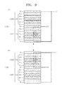
- FIG. 9 is a view for explaining a dual emission of the organic light-emitting diode OLED of FIG. 5 according to the timing diagram of FIG. 7 , according to an embodiment of the present invention.
- the fixed first power voltage V1 is applied to the top electrode TE and the bottom electrode BE
- the third voltage V21 is applied as the second power voltage V2 to the common electrode CE.
- the second organic light-emitting diode OLED2 formed between the top electrode TE and the common electrode CE is reverse-biased
- the first organic light-emitting diode OLED1 formed between the bottom electrode BE and the common electrode CE is forward-biased.
- the bottom electrode BE of the first organic light-emitting diode OLED1 functions as a hole injection electrode
- the common electrode CE functions as an electron injection electrode.
- Electrons move from the common electrode CE of the first organic light-emitting diode OLED1 through the EIL 25a and the ETL 24a, and holes move from the bottom electrode BE through the HIL 21a and the HTL 22a.
- the electrons and holes are combined in the EML 23a to form excitons, and due to energy from the formed excitons, light is emitted. Since the common electrode CE is a reflective electrode, the generated light is emitted toward the bottom electrode BE (front side).
- the fixed first power voltage V1 is applied to the top electrode TE and the bottom electrode BE
- the fourth voltage V22 is applied as the second power voltage V2 to the common electrode CE.
- the second organic light-emitting diode OLED2 formed between the top electrode TE and the common electrode CE is forward-biased
- the first organic light-emitting diode OLED1 formed between the bottom electrode BE and the common electrode CE is reverse-biased.
- the top electrode TE of the second organic light-emitting diode OLED2 functions as an electron injection electrode
- the common electrode CE functions as a hole injection electrode.
- Electrons are injected from the top electrode TE of the second organic light-emitting diode OLED2 through the EIL 25b and the ETL 24b, and holes are injected from the common electrode CE through the HIL 21b and the HTL 22b.
- the electrons and holes are combined in the EML 23b to form excitons, and due to energy from the formed excitons, light is emitted.
- the common electrode CE is a reflective electrode, the generated light is emitted toward the top electrode TE (back side).
- the second power voltage V2 applied to the organic light-emitting diode OLED varies to alternately control a front side emission and a back side emission to produce images on back and front sides.
- FIG. 10 is a view for explaining a dual emission of the organic light-emitting diode OLED of FIG. 6 according to the timing diagram of FIG. 7 , according to an embodiment of the present invention.
- the fixed first power voltage V1 is applied to the top electrode TE and the bottom electrode BE
- the third voltage V21 is applied as the second power voltage V2 to the common electrode CE. Accordingly, the first organic light-emitting diode OLED1 formed between the top electrode TE and the common electrode CE is forward-biased, and the second organic light-emitting diode OLED2 formed between the bottom electrode BE and the common electrode CE is reverse-biased.
- the top electrode TE of the first organic light-emitting diode OLED1 functions as a hole injection electrode
- the common electrode CE functions as an electron injection electrode. Electrons are injected from the common electrode CE of the first organic light-emitting diode OLED1 through the EIL 25a and the ETL 24a, and holes are injected from the top electrode TE through the HIL 21a and the HTL 22a. The electrons and holes are combined in the EML 23a to form excitons, and due to energy from the formed excitons, light is emitted. Since the common electrode CE is a reflective electrode, the generated light is emitted toward the top electrode TE (back side).
- the fixed first power voltage V1 is applied to the top electrode TE and the bottom electrode BE
- the fourth voltage V22 is applied as the second power voltage V2 to the common electrode CE. Accordingly, the first organic light-emitting diode OLED1 formed between the top electrode TE and the common electrode CE is reverse-biased, and the second organic light-emitting diode OLED2 formed between the bottom electrode BE and the common electrode CE is forward-biased.
- the bottom electrode BE of the second organic light-emitting diode OLED1 functions as an electron injection electrode
- the common electrode CE functions as a hole injection electrode. Electrons are injected from the bottom electrode BE of the second organic light-emitting diode OLED2 through the EIL 25b and the ETL 24b, and holes are injected from the common electrode CE through the HIL 21b and the HTL 22b. The electrons and holes are combined in the EML 23b to form excitons, and due to energy from the formed excitons, light is emitted. Since the common electrode CE is a reflective electrode, the generated light is emitted toward the bottom electrode BE (front side).
- the second power voltage V2 applied to the organic light-emitting diode OLED varies to alternately control a front side emission and a back side emission to produce images on back and front sides.
- FIG. 11 is a timing diagram for explaining a dual emission of an organic light-emitting diode OLED, according to another embodiment of the present invention.
- FIG. 12 is a circuit diagram illustrating a dual emission of the organic light-emitting diode OLED according to the timing diagram of FIG. 11 .
- the switching thin film transistor TRs is turned on to supply a data signal Dj supplied through a data line to the storage capacitor Cst.
- the second power voltage V2 is fixed and the first power voltage V1 alternately swings between the first voltage V11 and the second voltage V12. That is, during the first period T1, the first voltage V11 is applied as the first power voltage V1, and during the second period T2, the second voltage V12 is applied as the first power voltage V1.
- the first voltage V11 is a voltage with a lower level than the second power voltage V2
- the second voltage V12 is a voltage with a higher level than the second power voltage V2.
- the second power voltage V2 may be 12 V
- the first voltage V11 may be 0 V
- the second voltage V12 may be 24 V.
- Each of the first period T1 and the second period T2 may constitute one frame period, or the sum of the first period T1 and the second period T2 may constitute one frame period. That is, the first power voltage V1 may vary in every frame, or may vary within one frame.
- the driving thin film transistor TRd may, corresponding to a voltage stored in the storage capacitor Cst, control a current flowing between the first voltage V11 and the second power voltage V2 through the second organic light-emitting diode OLED2, and accordingly, as illustrated in FIG. 12(a) , the second organic light-emitting diode OLED2 emits light.
- the first power voltage V1 is transitioned to the second voltage V12 from the first voltage V11.
- the second organic light-emitting diode OLED 2 is reverse-biased and the first organic light-emitting diode OLED1 is forward-biased.
- the driving thin film transistor TRd may, corresponding to a voltage stored in the storage capacitor Cst, control a current flowing between the second voltage V12 and the second power voltage V2 through the first organic light-emitting diode OLED1, and accordingly, as illustrated in FIG. 12(b) , the first organic light-emitting diode OLED1 emits light.
- FIG. 13 is a view for explaining a dual emission of the organic light-emitting diode OLED of FIG. 5 according to the timing diagram of FIG. 11 , according to another embodiment of the present invention.
- the first voltage V11 is applied as the first power voltage V1 to the top electrode TE and the bottom electrode BE
- the fixed second power voltage V2 is applied to the common electrode CE.
- the second organic light-emitting diode OLED2 formed between the top electrode TE and the common electrode CE is forward-biased
- the first organic light-emitting diode OLED1 formed between the bottom electrode BE and the common electrode CE is reverse-biased.
- the top electrode TE of the second organic light-emitting diode OLED2 functions as an electron injection electrode
- the common electrode CE functions as a hole injection electrode.
- Electrons are injected from the top electrode TE of the second organic light-emitting diode OLED2 through the EIL 25b and the ETL 24b, and holes are injected from the common electrode CE through the HIL 21b and the HTL 22b.
- the electrons and holes are combined in the EML 23b to form excitons, and due to energy from the formed excitons, light is emitted.
- the common electrode CE is a reflective electrode, the generated light is emitted toward the top electrode TE (back side).
- the second voltage V12 is applied as the first power voltage V1 to the top electrode TE and the bottom electrode BE, and the fixed second power voltage V2 is applied to the common electrode CE.
- the second organic light-emitting diode OLED2 formed between the top electrode TE and the common electrode CE is reverse-biased, and the first organic light-emitting diode OLED1 formed between the bottom electrode BE and the common electrode CE is forward-biased.
- the bottom electrode BE of the first organic light-emitting diode OLED1 functions as a hole injection electrode
- the common electrode CE functions as an electron injection electrode.
- Electrons are injected from the common electrode CE of the first organic light-emitting diode OLED1 through the EIL 25a and the ETL 24a, and holes are injected from the bottom electrode BE through the HIL 21a and the HTL 22a.
- the electrons and holes are combined in the EML 23a to form excitons, and due to energy from the formed excitons, light is emitted. Since the common electrode CE is a reflective electrode, the generated light is emitted toward the bottom electrode BE (front side).
- the first power voltage V1 applied to the organic light-emitting diode OLED varies to alternately control a front side emission and a back side emission to produce images on back and front sides thereof.
- FIG. 14 is a view for explaining a dual emission of the organic light-emitting diode OLED of FIG. 6 according to the timing diagram of FIG. 11 , according to another embodiment of the present invention.
- the first voltage V11 is applied as the first power voltage V1 to the top electrode TE and the bottom electrode BE
- the fixed second power voltage V2 is applied to the common electrode CE.
- the second organic light-emitting diode OLED2 formed between the bottom electrode BE and the common electrode CE is forward-biased
- the first organic light-emitting diode OLED1 formed between the top electrode TE and the common electrode CE is reverse-biased.
- the bottom electrode BE of the second organic light-emitting diode OLED2 functions as an electron injection electrode
- the common electrode CE functions as a hole injection electrode.
- Electrons are injected from the bottom electrode BE of the second organic light-emitting diode OLED2 through the EIL 25b and the ETL 24b, and holes are injected from the common electrode CE through the HIL 21b and the HTL 22b.
- the electrons and holes are combined in the EML 23b to form excitons, and due to energy from the formed excitons, light is emitted.
- the common electrode CE is a reflective electrode, the generated light is emitted toward the bottom electrode BE (front side).
- the second voltage V12 is applied as the first power voltage V1 to the top electrode TE and the bottom electrode BE, and the fixed second power voltage V2 is applied to the common electrode CE.
- the second organic light-emitting diode OLED2 formed between the bottom electrode BE and the common electrode CE is reverse-biased, and the first organic light-emitting diode OLED1 formed between the top electrode TE and the common electrode CE is forward-biased.
- the top electrode TE of the first organic light-emitting diode OLED1 functions as a hole injection electrode
- the common electrode CE functions as an electron injection electrode.
- Electrons are injected from the common electrode CE of the first organic light-emitting diode OLED1 through the EIL 25a and the ETL 24a, and holes are injected from the top electrode TE through the HIL 21a and the HTL 22a.
- the electrons and holes are combined in the EML 23a to form excitons, and due to energy from the formed excitons, light is emitted. Since the common electrode CE is a reflective electrode, the generated light is emitted toward the top electrode TE (back side).
- the first power voltage V1 applied to the organic light-emitting diode OLED varies to alternately control a front side emission and a back side emission to produce images on back and front sides thereof.
- FIG. 15 is a timing diagram for explaining a dual emission of an organic light-emitting diode OLED, according to another embodiment of the present invention.
- FIG. 16 is a circuit diagram illustrating a dual emission of the organic light-emitting diode OLED according to the timing diagram of FIG. 15 .
- the switching thin film transistor TRs is turned on to supply a data signal Dj supplied through a data line to the storage capacitor Cst.
- the first power voltage V1 alternately swings between the first voltage V11 and the second voltage V12 and the second power voltage V2 alternately swings between the third voltage V21 and the fourth voltage V22.
- the first power voltage V1 and the second power voltage V2 may be inversion signals.
- the first voltage V11 and the third voltage V21 may be a voltage with an identical level
- the second voltage V12 and the fourth voltage V22 may be a voltage with an identical level.
- the first voltage V11 and the third voltage V21 may be 0 V
- the second voltage V12 and the fourth voltage V22 may be 12 V.
- Each of the first period T1 and the second period T2 may constitute one frame period, or the sum of the first period T1 and the second period T2 may constitute one frame period. That is, the first power voltage V1 and the second power voltage V2 may vary in every frame, or may vary within one frame.
- the driving thin film transistor TRd may, corresponding to a voltage stored in the storage capacitor Cst, control a current flowing between the second voltage V12 and the third voltage V21 through the first organic light-emitting diode OLED1, and accordingly, as illustrated in FIG. 16(a) , the first organic light-emitting diode OLED1 emits light.
- the first power voltage V1 is transitioned from the second voltage V12 to the first voltage V11
- the second power voltage V2 is transitioned from the third voltage V21 to the fourth voltage V22.
- the first organic light-emitting diode OLED1 is reverse-biased and the second organic light-emitting diode OLED2 is forward-biased.
- the driving thin film transistor TRd may, corresponding to a voltage stored in the storage capacitor Cst, control a current flowing between the first voltage V11 and the fourth voltage V22 through the second organic light-emitting diode OLED2, and accordingly, as illustrated in FIG. 16(b) , the second organic light-emitting diode OLED2 emits light.
- a data signal range may decrease, and thus, a voltage of a scan signal may decrease. Accordingly, power consumption of a driving circuit decreases and a lifetime of a display device increases.
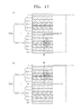
- FIG. 17 is a view for explaining a dual emission of the organic light-emitting diode OLED of FIG. 5 according to the timing diagram of FIG. 15 , according to another embodiment of the present invention.
- the second voltage V12 is applied as the first power voltage V1 to the top electrode TE and the bottom electrode BE
- the third voltage V21 is applied as the second power voltage V2 to the common electrode CE.
- the second organic light-emitting diode OLED2 formed between the top electrode TE and the common electrode CE is reverse-biased
- the first organic light-emitting diode OLED1 formed between the bottom electrode BE and the common electrode CE is forward-biased.
- the bottom electrode BE of the first organic light-emitting diode OLED1 functions as a hole injection electrode
- the common electrode CE functions as an electron injection electrode.
- Electrons are injected from the common electrode CE of the first organic light-emitting diode OLED1 through the EIL 25a and the ETL 24a, and holes are injected from the bottom electrode BE through the HIL 21a and the HTL 22a.
- the electrons and holes are combined in the EML 23a to form excitons, and due to energy from the formed excitons, light is emitted. Since the common electrode CE is a reflective electrode, the generated light is emitted toward the bottom electrode BE (front side).
- the first voltage V11 is applied as the first power voltage V1 to the top electrode TE and the bottom electrode BE
- the fourth voltage V22 is applied as the second power voltage V2 to the common electrode CE.
- the second organic light-emitting diode OLED2 formed between the top electrode TE and the common electrode CE is forward-biased
- the first organic light-emitting diode OLED1 formed between the bottom electrode BE and the common electrode CE is reverse-biased.
- the top electrode TE of the second organic light-emitting diode OLED2 functions as an electron injection electrode
- the common electrode CE functions as a hole injection electrode.
- Electrons are injected from the top electrode TE of the second organic light-emitting diode OLED2 through the EIL 25b and the ETL 24b, and holes are injected from the common electrode CE through the HIL 21b and the HTL 22b.
- the electrons and holes are combined in the EML 23b to form excitons, and due to energy from the formed excitons, light is emitted.
- the common electrode CE is a reflective electrode, the generated light is emitted toward the top electrode TE (back side).
- the first power voltage V1 and the second power voltage V2 applied to the organic light-emitting diode OLED vary to alternately control a front side emission and a back side emission to produce images on back and front sides.
- FIG. 18 is a view for explaining a dual emission of the organic light-emitting diode OLED of FIG. 6 according to the timing diagram of FIG. 15 , according to another embodiment of the present invention.
- the second voltage V12 is applied as the first power voltage V1 to the top electrode TE and the bottom electrode BE
- the third voltage V21 is applied as the second power voltage V2 to the common electrode CE.
- the first organic light-emitting diode OLED1 formed between the top electrode TE and the common electrode CE is forward-biased
- the second organic light-emitting diode OLED2 formed between the bottom electrode BE and the common electrode CE is reverse-biased.
- the top electrode TE of the first organic light-emitting diode OLED1 functions as a hole injection electrode
- the common electrode CE functions as an electron injection electrode.
- Electrons are injected from the common electrode CE of the first organic light-emitting diode OLED1 through the EIL 25a and the ETL 24a, and holes are injected from the top electrode TE through the HIL 21a and the HTL 22a.
- the electrons and holes are combined in the EML 23a to form excitons, and due to energy from the formed excitons, light is emitted. Since the common electrode CE is a reflective electrode, the generated light is emitted toward the top electrode TE (back side).
- the first voltage V11 is applied as the first power voltage V1 to the top electrode TE and the bottom electrode BE
- the fourth voltage V22 is applied as the second power voltage V2 to the common electrode CE.
- the first organic light-emitting diode OLED1 formed between the top electrode TE and the common electrode CE is reverse-biased
- the second organic light-emitting diode OLED2 formed between the bottom electrode BE and the common electrode CE is forward-biased.
- the bottom electrode BE of the second organic light-emitting diode OLED2 functions as an electron injection electrode
- the common electrode CE functions as a hole injection electrode.
- Electrons are injected from the bottom electrode BE of the second organic light-emitting diode OLED2 through the EIL 25b and the ETL 24b, and holes are injected from the common electrode CE through the HIL 21b and the HTL 22b.
- the electrons and holes are combined in the EML 23b to form excitons, and due to energy from the formed excitons, light is emitted.
- the common electrode CE is a reflective electrode, the generated light is emitted toward the bottom electrode BE (front side). That is, according to the present embodiment, the first power voltage V1 and the second power voltage V2 applied to the organic light-emitting diode OLED vary to alternately control a front side emission and a back side emission to produce images on back and front sides thereof.
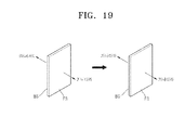
- FIG. 19 is a view for illustrating a dual emission according to embodiments of the present invention and a dual emission according to a comparative embodiment.
- a display device including a typical organic light-emitting diode including an anode, a cathode, and an organic EML interposed between the anode and the cathode is illustrated, and the transmittancy of the anode and cathode of the display device is controlled to perform a dual emission.
- an image is embodied on both sides.
- this is a simple change of an emission direction toward the front side FS into an emission direction toward the back side BS, and thus, an image on the front side FS and an image on the back side BS are inversed, and thus, delivery of desired information is impossible.
- a dual emission according to an embodiment of the present invention illustrated on the right side of FIG. 19 may be embodied using such a structure including two organic layers each including an EML and an intermediate electrode formed between top and bottom electrodes, and according to a variation of a power voltage, time-sharing emission is performed on the front side FS and the back side BS in each pixel. Accordingly, an image on the front side FS and the back side BS may not have to be inversed.
- two organic layers are deposited in each pixel, and an intermediate electrode is used to control front side emission and back side emission according to an input signal in each pixel, thereby providing a dual emission display producing different images on a front side and a back side in each pixel.
- the present invention is not limited thereto, and may also be applied to a pixel including an organic light-emitting diode having a stack structure according to the present invention, a plurality of thin film transistors, and a plurality of capacitors.
- An organic light-emitting display device overcomes the problems of a typical dual emission display device, such as reversion of an image or the requirement of manufacturing two panels, and embodies a dual emission display device that emits light in two directions in each pixel without reversion of an image.
Landscapes
- Engineering & Computer Science (AREA)
- Microelectronics & Electronic Packaging (AREA)
- Physics & Mathematics (AREA)
- Optics & Photonics (AREA)
- Manufacturing & Machinery (AREA)
- Electroluminescent Light Sources (AREA)
- Control Of El Displays (AREA)
- Devices For Indicating Variable Information By Combining Individual Elements (AREA)
Abstract
Description
- The following description relates to an organic light-emitting diode, an organic light-emitting display device including the same, and a method of controlling dual emission of the organic light-emitting diode.
- Among various flat panel display devices, organic light-emitting display devices are self-emission display devices that electrically excite an organic compound to emit light. Such organic light-emitting display devices are manufactured at a low temperature, have high response speeds, have low power consumption, self-emit light, and have wide-viewing angles. In addition, organic light-emitting display devices have high contrast characteristics and do not require a backlight, which is required by a liquid crystal display (LCD), thereby enabling the production of lightweight and thin devices. In addition, organic light-emitting display devices have uniform surface emission characteristics and are easy to manufacture, and due to such characteristics, they are used in mobile phones.
- Recently, research into dual-emission organic light-emitting display devices that can emit light on front and back sides thereof is being performed. In the case of a single panel, front and back side images (produced by an organic light-emitting display that emits light in two directions by controlling two electrodes of an organic light-emitting diode) are reversed images. On the other hand, when two panels are separately manufactured and then attached to each other, the attachment of the two panels results in high manufacturing costs, increased thickness, high consumption costs, or the like.
- Aspects of embodiments of the present invention are directed toward various display modes with relatively small occupation space by selectively or simultaneously supplying identical or different images on front and back sides via a single panel.
- According to an embodiment of the present invention, there is provided an organic light-emitting diode including: a first electrode and a second electrode facing each other; a common electrode interposed between the first electrode and the second electrode; a first organic layer interposed between the first electrode and the common electrode; and a second organic layer that is interposed between the second electrode and the common electrode and is reverse-symmetric to the first organic layer with respect to the common electrode.
- In one embodiment, the first organic layer includes a hole injection layer, a hole transfer layer, an emission layer, an electron transfer layer, and an electron injection layer, sequentially disposed in this order on the first electrode, and the second organic layer includes an electron injection layer, an electron transfer layer, an emission layer, a hole transfer layer, and a hole injection layer, sequentially disposed in this order on the second electrode.
- In one embodiment, the first electrode is a bottom electrode, and the second electrode is a top electrode. In another embodiment, the first electrode is a top electrode, and the second electrode is a bottom electrode.
- In one embodiment, a first power voltage is applied to the first electrode and the second electrode, and a second power voltage is applied to the common electrode, and according to a variation of the first power voltage and/or the second power voltage, the common electrode functions as an electron injection electrode or a hole injection electrode.
- Each of the first electrode and the second electrode may be a transparent electrode or a semi-transparent electrode. The common electrode may be a reflective electrode.
- One of the first electrode and the second electrode may be formed on a substrate.
- According to another embodiment of the present invention, there is provided a method of controlling a dual emission of an organic light-emitting diode, wherein the organic light-emitting diode includes a first electrode, a second electrode, a pair of organic layers disposed between the first and second electrodes, and a common electrode that divides the organic layers between the first electrode and the second electrode, wherein the method includes: applying a first power voltage to the first electrode and the second electrode; and applying a second power voltage to the common electrode, wherein the first power voltage and/or the second power voltage varies and the organic layers alternately emit light toward the first electrode and the second electrode in response to this variation.
- The applying of the second power voltage may include alternately applying a second power voltage with higher and lower levels than the first power voltage to the common electrode.
- The applying of the first power voltage may include alternately applying a first power voltage with higher and lower levels than the second power voltage to the first electrode and the second electrode.
- The applying of the first power voltage may include applying the first power voltage with a first level and a second level that is higher than the first level, and the applying of the second power voltage may include alternately applying the second power voltage with the first level and the second level, wherein the first power voltage and the second power voltage are inversion voltages.
- According to another embodiment of the present invention, provided is an organic light-emitting display device including: a plurality of organic light-emitting diodes including a first electrode, a second electrode, a common electrode interposed between the first electrode and the second electrode, and a pair of organic layers that are reverse-symmetric to each other with respect to the common electrode between the first electrode and the second electrode; and a power supplier applying a first power voltage to the first and second electrodes and a second power voltage to the common electrode and varying the first power voltage and/or the second power voltage, wherein each of the organic light-emitting diodes emits light either toward the first electrode or toward the second electrode according to the varied first power voltage and second power voltage.
- In one embodiment, the power supplier fixes the first power voltage and applies the second power voltage with higher and lower levels than the first power voltage to the common electrode.
- In one embodiment, the power supplier fixes the second power voltage and applies the first power voltage with higher and lower levels than the second power voltage to the first electrode and the second electrode.
- In one embodiment, the power supplier alternately applies the first power voltage with a first level and a second level that is higher than the first level, and simultaneously, alternately applies the second power voltage with the first level and the second level, wherein the first power voltage and the second power voltage are inversion voltages.
- In one embodiment, the first power voltage and/or the second power voltage varies in every frame or within one frame.
- In one embodiment, one of the first electrode and the second electrode is formed on a substrate.
- In one embodiment, each of the first electrode and the second electrode is a transparent electrode or a semi-transparent electrode, and the common electrode is a reflective electrode.
- According to an aspect of the present invention, there is provided a dual emission organic light-emitting diode arrangement as set out in claim 1. Preferred features of this aspect are set out in claims 2 to 6.
- According to another aspect of the present invention, there is provided a method of controlling a dual emission of an organic light-emitting diode arrangement as set out in claim 7. Preferred features of this aspect are set out in claims 8 to 10.
- According to another aspect of the present invention, there is provided an organic light-emitting display device as set out in claim 11. Preferred features of this aspect are set out in claims 12 to 14.
- The above and other features and advantages of the present invention will become more apparent by describing in detail exemplary embodiments thereof with reference to the attached drawings in which:
-
FIG. 1 is a schematic block diagram of an organic light-emitting display device according to an embodiment of the present invention; -
FIG. 2 is an equivalent circuit diagram of a pixel illustrated inFIG. 1 according to an embodiment of the present invention; -
FIG. 3 is a graph of current density versus voltage characteristics of a dual emission display device according to an embodiment of the present invention; -
FIG. 4 is a graph of brightness versus voltage characteristics of a dual emission display device according to an embodiment of the present invention; -
FIG. 5 is a schematic cross-sectional view of an organic light-emitting diode ofFIG. 2 , according to an embodiment of the present invention; -
FIG. 6 is a schematic cross-sectional view of the organic light-emitting diode ofFIG. 2 , according to another embodiment of the present invention; -
FIG. 7 is a timing diagram for explaining a dual emission of an organic light-emitting diode, according to an embodiment of the present invention; -
FIG. 8 is a diagram illustrating a dual emission of an organic light-emitting diode according to the timing diagram ofFIG. 7 ; -
FIG. 9 is a view for explaining a dual emission of the organic light-emitting diode of -
FIG. 5 according to the timing diagram ofFIG. 7 , according to an embodiment of the present invention; -
FIG. 10 is a view for explaining a dual emission of the organic light-emitting diode of -
FIG. 6 according to the timing diagram ofFIG. 7 , according to an embodiment of the present invention; -
FIG. 11 is a timing diagram for explaining a dual emission of an organic light-emitting diode, according to another embodiment of the present invention; -
FIG. 12 is a diagram illustrating a dual emission of an organic light-emitting diode according to the timing diagram ofFIG. 11 ; -
FIG. 13 is a view for explaining a dual emission of the organic light-emitting diode of -
FIG. 5 according to the timing diagram ofFIG. 11 , according to another embodiment of the present invention; -
FIG. 14 is a view for explaining a dual emission of the organic light-emitting diode of -
FIG. 6 according to the timing diagram ofFIG. 11 , according to another embodiment of the present invention; -
FIG. 15 is a timing diagram for explaining a dual emission of an organic light-emitting diode, according to another embodiment of the present invention; -
FIG. 16 is a diagram illustrating a dual emission of an organic light-emitting diode according to the timing diagram ofFIG. 15 ; -
FIG. 17 is a view for explaining a dual emission of the organic light-emitting diode of -
FIG. 5 according to the timing diagram ofFIG. 15 , according to another embodiment of the present invention; -
FIG. 18 is a view for explaining a dual emission of the organic light-emitting diode of -
FIG. 6 according to the timing diagram ofFIG. 15 , according to another embodiment of the present invention; and -
FIG. 19 is a view for illustrating a dual emission according to embodiments of the present invention and a dual emission according to a comparative embodiment. - As the invention allows for various changes and numerous embodiments, particular embodiments will be illustrated in the drawings and described in detail in the written description. However, this is not intended to limit the present invention to particular modes of practice, and it is to be appreciated that all changes, equivalents, and substitutes that do not depart from the spirit and technical scope of the present invention are encompassed in the present invention.
- In the description of the present invention, certain detailed explanations of related art are omitted when it is deemed that they may unnecessarily obscure the essence of the invention, and throughout the specification, like reference numerals refer to like elements.
- In addition, in the drawings, sizes and thickness of constituents are arbitrarily illustrated to obtain ease of description, and thus, the present invention is not limited thereto.
- In the drawings, the thicknesses of layers and regions are exaggerated for clarity. Also, in the drawings, the thicknesses of layers and regions are exaggerated for ease of description. It will also be understood that when a layer, a film, a region, a plate, or the like is referred to as being "on" another layer or substrate, it can be 'directly on' the other constituent, or intervening layers may also be present.
- In the present specification, it is to be understood that the terms such as "including" are intended to indicate the existence of constituents disclosed in the specification, and are not intended to preclude the possibility that other constituents may exist, but may be added. Also, in the specification, the term "on" indicates being above or under other constituents, and it is not necessary that a constituent exists only above other constituents with respect to a gravity direction.
-
FIG. 1 is a schematic block diagram of an organic light-emittingdisplay device 10 according to an embodiment of the present invention. - Referring to
FIG. 1 , the organic light-emittingdisplay device 10 according to the present embodiment includes adisplay panel 100, ascan driver 200, adata driver 300, acontroller 400, and apower supplier 500. - The organic light-emitting
display device 10 may selectively or simultaneously provide identical or different images on front and back sides thereof through thedisplay panel 100. - The
display panel 100 includes a plurality of scan lines SL1 to SLn that are spaced apart from each other and aligned in rows and a plurality of data lines DL1 to DLm that are spaced apart from each other and aligned in columns, wherein the scan lines SL1 to SLn and the data lines DL1 to DLm are aligned in a matrix form. A pixel PX is located near each of the intersections (crossing regions) of the scan lines SL1 to SLn and the data lines DL1 to DLm, and thus, the pixels PX are aligned in a matrix form. An alignment direction of pixels PX in each row, that is, a direction along a scan line for selecting a row is referred to as a row direction, and an alignment direction of pixels PX in each column, that is, a direction perpendicular to the scan line is referred to as a column direction. - The
scan driver 200 may generate scan signals and may sequentially supply the scan signals to thedisplay panel 100 through the scan lines SL1 to SLn. - The
data driver 300 may generate data signals and may sequentially supply the data signals to thedisplay panel 100 through the data lines DL1 to DLm. Thedata driver 300 converts input image data DATA having gradation input from thecontroller 400 into a data signal in the form of a voltage or a current. - The
controller 400 generates a scan control signal CS1 and a data control signal CS2 and transmits the scan control signal CS1 and the data control signal CS2 to thescan driver 200 and thedata driver 300, respectively. Accordingly, thescan driver 200 sequentially applies scan signals through scan lines, and thedata driver 300 applies data signals to pixels. Thecontroller 400 outputs image data DATA to thedata driver 300. - The
controller 400 may drive thedisplay panel 100 in a single emission mode for operating one of a front side and a back side or a dual emission mode for operating both front and back sides of thedisplay panel 100. In the dual emission mode, thecontroller 400 may control thepower supplier 500 in such a manner that the front and back sides of thedisplay panel 100 alternately emit light to display an image. - The
power supplier 500 converts a voltage input by an external power source, such as a battery, into a first power voltage V1 and a second power voltage V2 for the emission of a light-emitting device of thedisplay panel 100. Thepower supplier 500, under control of thecontroller 400, varies at least one of the first power voltage V1 or the second power voltage V2 and applies the varied voltage to thedisplay panel 100. Thepower supplier 500 may use a direct current-direct current (DC-DC) converter. -
FIG. 2 is an equivalent circuit diagram of a pixel PX inFIG. 1 according to an embodiment of the present invention. - Referring to
FIG. 2 , the pixel PX may include two thin film transistors and one capacitor. - The pixel PX may include an organic light-emitting diode OLED, a driving thin film transistor TRd, a switching thin film transistor TRs, and a storage capacitor Cst, connected between a first power voltage V1 and a second power voltage V2.
- The organic light-emitting diode OLED includes a first organic light-emitting diode OLED1 that emits light on one of front and rear sides of the
display panel 100, and a second organic light-emitting diode OLED2 that emits light on the other side thereof. - The
display panel 100 time-sharing drives the first organic light-emitting diode OLED1 and the second organic light-emitting diode OLED2 of the pixel PX to express an image on a front side and a back side thereof. Herein, the front side and the back side are not particularly defined, and a side typically viewed by a user may be referred to as the front side and the opposite side may be referred to as the back side. In this regard, the front side may be bottom emission and the back side may be top emission, and according to another embodiment, the front side may be bottom emission and the back side may be top emission. - The driving thin film transistor TRd controls a current flowing between the first power voltage V1 and the second power voltage V2 through the first organic light-emitting diode OLED1 or the second organic light-emitting diode OLED2, corresponding to a voltage stored in the storage capacitor Cst during emission of the pixel PX. A gate electrode of the driving thin film transistor TRd is connected to a first terminal of the storage capacitor Cst, and the source electrode S1 of the driving thin film transistor TRd is connected to a second terminal of the storage capacitor Cst and the first power voltage V1. In addition, a drain electrode of the driving thin film transistor TRd is connected to an anode of the first organic light-emitting diode OLED1 and a cathode of the second organic light-emitting diode OLED2.
- The switching thin film transistor TRs is connected to and interposed between a data line DLj and the driving thin film transistor TRd, and when a scan signal Si is supplied through a scan line SLi, the switching thin film transistor TRs is turned on to supply the data signal Dj supplied through the data line DLj to the storage capacitor Cst. The storage capacitor Cst is charged with a voltage corresponding to the data signal Dj. That is, a gate electrode of the switching thin film transistor TRs is connected to the scan line SLi, and a source electrode thereof is connected to the data line DLj. A drain electrode of the switching thin film transistor TRs is connected to the first terminal of the storage capacitor Cst.
- The anode of the first organic light-emitting diode OLED1 and the cathode of the second organic light-emitting diode OLED2 are connected to the first power voltage V1 through the driving thin film transistor TRd. A cathode of the first organic light-emitting diode OLED1 and an anode of the second organic light-emitting diode OLED2 are connected to the second power voltage V2. The cathode of the first organic light-emitting diode OLED1 and the anode of the second organic light-emitting diode OLED2 are a common electrode. That is, the common electrode functions as the cathode of the first organic light-emitting diode OLED1 and the anode of the second organic light-emitting diode OLED2. Here, the first organic light-emitting diode OLED1 and the second organic light-emitting diode OLED2, when the first power voltage V1 and the second power voltage V2 are applied thereto, emit light with brightness corresponding to a driving current flowing in the first organic light-emitting diode OLED1 and the second organic light-emitting diode OLED2.
- The first power voltage V1 may be a fixed voltage or a variable voltage. In the latter case, the first power voltage V1 may be changed to a first voltage V11 or a second voltage V12 with a higher level than the first voltage V11. The second power voltage V2 may be a fixed voltage or a variable voltage. In the latter case, the second power voltage V2 may be changed to a third voltage V21 or a fourth voltage V22 with a higher level than the third voltage V21.
- Since at least one of the first power voltage V1 or the second power voltage V2 varies, the first organic light-emitting diode OLED1 and the second organic light-emitting diode OLED2 are alternately forward-biased or reverse-biased. For example, when the first organic light-emitting diode OLED1 is forward-biased, the second organic light-emitting diode OLED2 is reverse-biased and the first organic light-emitting diode OLED1 emits light (and the second organic light-emitting diode OLED2 does not). On the other hand, when the first organic light-emitting diode OLED1 is reverse-biased, the second organic light-emitting diode OLED2 is forward-biased and emits light.
- That is, according to the present invention, if the first organic light-emitting diode OLED1 is reverse-biased, the second organic light-emitting diode OLED2 emits light, and if the second organic light-emitting diode OLED2 is reverse-biased, the first organic light-emitting diode OLED1 emits light, thereby embodying dual emission.
-
FIG. 3 is a graph of current density versus voltage characteristics of a dual display device according to an embodiment of the present invention.FIG. 4 is a graph of luminance versus voltage characteristics of a dual display device according to an embodiment of the present invention. - A typical organic light-emitting diode OLED shows diode characteristics, that is, during a reverse bias, a current does not flow. However, according to embodiments of the present invention, since the first organic light-emitting diode OLED1 and the second organic light-emitting diode OLED2 are reverse-symmetric to each other with respect to the common electrode (i.e. connected in parallel with opposite forward directions), as illustrated in
FIGS. 3 and 4 , even during a reverse bias, a current flows substantially like during the forward bias. Accordingly, time-sharing dual emission is possible. -
FIG. 5 is a schematic cross-sectional view of an organic light-emitting diode OLED ofFIG. 2 , according to an embodiment of the present invention. - Referring to
FIG. 5 , the organic light-emitting diode OLED according to the present embodiment includes a bottom electrode BE, a top electrode TE facing the bottom electrode BE, a common electrode CE disposed between the bottom electrode BE and the top electrode TE, and a pair of organic layers, namely, first and secondorganic layer 20a and 20b, that face each other and are reverse-symmetric to each other with respect 7to the common electrode CE. Accordingly, the organic light-emitting diode OLED includes the first organic light-emitting diode OLED1 and the second organic light-emitting diode OLED2, wherein the first organic light-emitting diode OLED1 includes the bottom electrode BE, the common electrode CE, and the first organic layer 20a between the bottom electrode BE and the common electrode CE, and the second organic light-emitting diode OLED2 includes the top electrode TE, the common electrode CE, and the secondorganic layer 20b between the top electrode TE and the common electrode CE. - The bottom electrode BE and the top electrode TE may be located at ends of the organic light-emitting diode OLED as a whole, and one of the bottom electrode BE and the top electrode TE may be formed on a substrate (not shown). Regarding each of the
organic layers 20a and 20b, the bottom electrode BE and the top electrode TE may be formed of a transparent or semi-transparent material to transmit emitted light therethrough. To obtain an effective light transmission, the bottom electrode BE and the top electrode TE may each have transmittance of 70% or more. For example, the bottom electrode BE and the top electrode TE may each be formed of indium tin oxide (ITO), indium zinc oxide (IZO), tin oxide (Sn02), zinc oxide (ZnO), aluminum zinc oxide, or a combination thereof. - The common electrode CE may be a reflective electrode formed of a metal thin film. A material for forming the reflective electrode may be lithium (Li), magnesium (Mg), silver (Ag), aluminum (Al), aluminum-lithium (Al-Li), calcium (Ca), magnesium-indium (Mg-In), magnesium-silver (Mg-Ag), or the like.
- The
power supplier 500 may apply the first power voltage V1 to the bottom electrode BE and the top electrode TE, and may apply the second power voltage V2 to the common electrode CE. According to voltage levels of the first power voltage V1 and the second power voltage V2, the bottom electrode BE, the top electrode TE, and the common electrode CE may function as a hole injection electrode or an electron injection electrode. - The first organic layer 20a may have a stack structure of a hole injection layer (HIL) 21a, a hole transfer layer or hole transport layer (HTL) 22a, an emission layer (EML) 23a, an electron transfer layer or electron transport layer (ETL) 24a, and an electron injection layer (EIL) 25a, which are sequentially stacked on the bottom electrode BE in this order.
- The second
organic layer 20b may have a stack structure of anEIL 25b, anETL 24b, anemission EML 23b, anHTL 22b, and anHIL 21b, which are sequentially stacked on the top electrode TE in this order. - As a material for forming the
HILs
a phthalocyanine compound, such as a copper phthalocyanine;
a star-burst type amine derivative, such as TCTA, m-MTDATA, m-MTDAPB, or MoO3; and
a conductive polymer with solubility, such as polyaniline/dodecylbenzenesulfonic acid (Pani/DBSA), poly(3,4-ethylenedioxythiophene)/poly(4-styrenesulfonate) (PEDOT/PSS), polyaniline/camphor sulfonic acid (Pani/CSA), and polyaniline-poly(4-styrenesulfonate) (PANI-PSS). - As a material for forming the
HTLs
a carbazole derivative, such as N-phenylcarbazole or polyvinylcarbazole, and
a typical amine derivative with an aromatic condensation ring, such as N,N'-bis(3-methylphenyl)-N,N'-diphenyl-[1,1-biphenyl]-4,4'-diamine (TPD), or N,N'-di(naphthalene-1-yl)-N,N'-diphenyl benzidine (α-NPD). - The
EMLs EMLs - Each of the
EMLs EMLs EMLs - A material for forming the
ETLs - A material for forming the
EILs EILs HILs EILs -
FIG. 6 is a schematic cross-sectional view of the organic light-emitting diode OLED ofFIG. 2 , according to another embodiment of the present invention. The organic light-emitting diode OLED ofFIG. 6 is distinguished from the organic light-emitting diode OLED ofFIG. 5 , in terms of the stack sequence order of the first and secondorganic layers 20a and 20b. - The organic light-emitting diode OLED according to the present embodiment includes a pair of the bottom electrode BE and the top electrode TE, the common electrode CE disposed between the bottom electrode BE and the top electrode TE, and the first and second
organic layers 20a and 20b that face each other and are reverse-symmetric to each other with respect to the common electrode CE. Accordingly, the organic light-emitting diode OLED includes the first organic light-emitting diode OLED1 and the second organic light-emitting diode OLED2, wherein the first organic light-emitting diode OLED1 includes the top electrode TE, the common electrode CE, and the first organic layer 20a between the top electrode TE and the common electrode CE, and the second organic light-emitting diode OLED2 includes the bottom electrode BE, the common electrode CE, and the secondorganic layer 20b between the bottom electrode BE and the common electrode CE. - The bottom electrode BE and the top electrode TE may be located at ends of the organic light-emitting diode OLED, and one of the bottom electrode BE and the top electrode TE may be formed on a substrate (not shown). Regarding each of the first and second
organic layers 20a and 20b, the bottom electrode BE and the top electrode TE may be formed of a transparent or semi-transparent material to transmit emitted light therethrough. To obtain an effective light transmission, the bottom electrode BE and the top electrode TE may each have transmittance of 70% or more. For example, the bottom electrode BE and the top electrode TE may each be formed of indium tin oxide (ITO), indium zinc oxide (IZO), tin oxide (Sn02), zinc oxide (ZnO), aluminum zinc oxide, or a combination thereof. - The common electrode CE may be a reflective electrode formed of a metal thin film. A material for forming the reflective electrode may be lithium (Li), magnesium (Mg), silver (Ag), aluminum (Al), aluminum-lithium (Al-Li), calcium (Ca), magnesium-indium (Mg-In), magnesium-silver (Mg-Ag), or the like.
- The
power supplier 500 may apply the first power voltage V1 to the bottom electrode BE and the top electrode TE, and may apply the second power voltage V2 to the common electrode CE. According to voltage levels of the first power voltage V1 and the second power voltage V2, the bottom electrode BE, the top electrode TE, and the common electrode CE may function as a hole injection electrode or an electron injection electrode. - The first organic layer 20a may have a stack structure of an
HIL 21a, anHTL 22a, anEML 23a, anETL 24a, and anEIL 25a, which are sequentially stacked on the top electrode TE in this order. - The second
organic layer 20b may have a stack structure of anEIL 25b, anETL 24b, anEML 23b, anHTL 22b, and anHIL 21b, which are sequentially stacked on the bottom electrode BE in this order. - The materials for forming the layers that constitute the first organic layer 20a and the second
organic layer 20b are the same as those for forming the layers that constitute the first organic layer 20a and the secondorganic layer 20b illustrated inFIG. 5 , and accordingly, will not be described again. -
FIG. 7 is a timing diagram for explaining a dual emission of an organic light-emitting diode OLED, according to an embodiment of the present invention.FIG. 8 is a circuit diagram illustrating a dual emission of the organic light-emitting diode OLED according to the timing diagram ofFIG. 7 . - Referring to
FIGS. 7 and8 , when a scan signal Si is supplied through a scan line, the switching thin film transistor TRs is turned on to supply a data signal Dj supplied through a data line to the storage capacitor Cst. - In this regard, the first power voltage V1 is fixed and the second power voltage V2 alternately swings between a third voltage V21 and a fourth voltage V22. That is, during a first period T1, the third voltage V21 is applied as the second power voltage V2, and during a second period T2, the fourth voltage V22 is applied as the second power voltage V2. The third voltage V21 is a voltage with a lower level than the first power voltage V1, and the fourth voltage V22 is a voltage with a higher level than the first power voltage V1. For example, the first power voltage V1 may be 12 V, the third voltage V21 may be 0 V, and the fourth voltage V22 may be 24 V. Each of the first period T1 and the second period T2 may constitute one frame period, or the sum of the first period T1 and the second period T2 may constitute one frame period. That is, the second power voltage V2 may vary in every frame, or may vary within one frame.
- During the first period T1, when the first power voltage V1 and the third voltage V21 are applied, the first organic light-emitting diode OLED1 is forward-biased and the second organic light-emitting diode OLED2 is reverse-biased. The driving thin film transistor TRd may, corresponding to a voltage stored in the storage capacitor Cst, control a current flowing between the first power voltage V1 and the third voltage V21 through the first organic light-emitting diode OLED1, and accordingly, as illustrated in
FIG. 8(a) , the first organic light-emitting diode OLED1 emits light. - During the second period T2, the second power voltage V2 is transitioned to the fourth voltage V22 from the third voltage V21. During the second period T2, when the first power voltage V1 and the fourth voltage V22 are applied, the second organic light-emitting diode OLED2 is forward-biased and the first organic light-emitting diode OLED1 is reverse-biased. The driving thin film transistor TRd may, corresponding to a voltage stored in the storage capacitor Cst, control a current flowing between the first power voltage V1 and the fourth voltage V22 through the second organic light-emitting diode OLED2, and accordingly, as illustrated in
FIG. 8(b) , the second organic light-emitting diode OLED2 emits light. -
FIG. 9 is a view for explaining a dual emission of the organic light-emitting diode OLED ofFIG. 5 according to the timing diagram ofFIG. 7 , according to an embodiment of the present invention. - Referring to
FIGS. 7 and9(a) , during the first period T1, the fixed first power voltage V1 is applied to the top electrode TE and the bottom electrode BE, and the third voltage V21 is applied as the second power voltage V2 to the common electrode CE. Accordingly, the second organic light-emitting diode OLED2 formed between the top electrode TE and the common electrode CE is reverse-biased, and the first organic light-emitting diode OLED1 formed between the bottom electrode BE and the common electrode CE is forward-biased. Thus, the bottom electrode BE of the first organic light-emitting diode OLED1 functions as a hole injection electrode, and the common electrode CE functions as an electron injection electrode. - Electrons move from the common electrode CE of the first organic light-emitting diode OLED1 through the
EIL 25a and theETL 24a, and holes move from the bottom electrode BE through theHIL 21a and theHTL 22a. The electrons and holes are combined in theEML 23a to form excitons, and due to energy from the formed excitons, light is emitted. Since the common electrode CE is a reflective electrode, the generated light is emitted toward the bottom electrode BE (front side). - Referring to
FIGS. 7 and9(b) , during the second period T2, the fixed first power voltage V1 is applied to the top electrode TE and the bottom electrode BE, and the fourth voltage V22 is applied as the second power voltage V2 to the common electrode CE. Accordingly, the second organic light-emitting diode OLED2 formed between the top electrode TE and the common electrode CE is forward-biased, and the first organic light-emitting diode OLED1 formed between the bottom electrode BE and the common electrode CE is reverse-biased. Thus, the top electrode TE of the second organic light-emitting diode OLED2 functions as an electron injection electrode, and the common electrode CE functions as a hole injection electrode. - Electrons are injected from the top electrode TE of the second organic light-emitting diode OLED2 through the
EIL 25b and theETL 24b, and holes are injected from the common electrode CE through theHIL 21b and theHTL 22b. The electrons and holes are combined in theEML 23b to form excitons, and due to energy from the formed excitons, light is emitted. Since the common electrode CE is a reflective electrode, the generated light is emitted toward the top electrode TE (back side). - That is, according to the present embodiment, the second power voltage V2 applied to the organic light-emitting diode OLED varies to alternately control a front side emission and a back side emission to produce images on back and front sides.
-
FIG. 10 is a view for explaining a dual emission of the organic light-emitting diode OLED ofFIG. 6 according to the timing diagram ofFIG. 7 , according to an embodiment of the present invention. - Referring to
FIGS. 7 and10(a) , during the second period T1, the fixed first power voltage V1 is applied to the top electrode TE and the bottom electrode BE, and the third voltage V21 is applied as the second power voltage V2 to the common electrode CE. Accordingly, the first organic light-emitting diode OLED1 formed between the top electrode TE and the common electrode CE is forward-biased, and the second organic light-emitting diode OLED2 formed between the bottom electrode BE and the common electrode CE is reverse-biased. - Thus, the top electrode TE of the first organic light-emitting diode OLED1 functions as a hole injection electrode, and the common electrode CE functions as an electron injection electrode. Electrons are injected from the common electrode CE of the first organic light-emitting diode OLED1 through the
EIL 25a and theETL 24a, and holes are injected from the top electrode TE through theHIL 21a and theHTL 22a. The electrons and holes are combined in theEML 23a to form excitons, and due to energy from the formed excitons, light is emitted. Since the common electrode CE is a reflective electrode, the generated light is emitted toward the top electrode TE (back side). - Referring to
FIGS. 7 and10(b) , during the second period T2, the fixed first power voltage V1 is applied to the top electrode TE and the bottom electrode BE, and the fourth voltage V22 is applied as the second power voltage V2 to the common electrode CE. Accordingly, the first organic light-emitting diode OLED1 formed between the top electrode TE and the common electrode CE is reverse-biased, and the second organic light-emitting diode OLED2 formed between the bottom electrode BE and the common electrode CE is forward-biased. - Thus, the bottom electrode BE of the second organic light-emitting diode OLED1 functions as an electron injection electrode, and the common electrode CE functions as a hole injection electrode. Electrons are injected from the bottom electrode BE of the second organic light-emitting diode OLED2 through the
EIL 25b and theETL 24b, and holes are injected from the common electrode CE through theHIL 21b and theHTL 22b. The electrons and holes are combined in theEML 23b to form excitons, and due to energy from the formed excitons, light is emitted. Since the common electrode CE is a reflective electrode, the generated light is emitted toward the bottom electrode BE (front side). - That is, according to the present embodiment, the second power voltage V2 applied to the organic light-emitting diode OLED varies to alternately control a front side emission and a back side emission to produce images on back and front sides.
-
FIG. 11 is a timing diagram for explaining a dual emission of an organic light-emitting diode OLED, according to another embodiment of the present invention.FIG. 12 is a circuit diagram illustrating a dual emission of the organic light-emitting diode OLED according to the timing diagram ofFIG. 11 . - Referring to
FIGS. 11 and12 , when a scan signal Si is supplied through a scan line, the switching thin film transistor TRs is turned on to supply a data signal Dj supplied through a data line to the storage capacitor Cst. - In this regard, the second power voltage V2 is fixed and the first power voltage V1 alternately swings between the first voltage V11 and the second voltage V12. That is, during the first period T1, the first voltage V11 is applied as the first power voltage V1, and during the second period T2, the second voltage V12 is applied as the first power voltage V1. The first voltage V11 is a voltage with a lower level than the second power voltage V2, and the second voltage V12 is a voltage with a higher level than the second power voltage V2. For example, the second power voltage V2 may be 12 V, the first voltage V11 may be 0 V, and the second voltage V12 may be 24 V. Each of the first period T1 and the second period T2 may constitute one frame period, or the sum of the first period T1 and the second period T2 may constitute one frame period. That is, the first power voltage V1 may vary in every frame, or may vary within one frame.
- During the first period T1, when the first voltage V11 and the second power voltage V2 are applied to the pixel PX, the first organic light-emitting diode OLED1 is reverse-biased and the second organic light-emitting diode OLED2 is forward-biased. The driving thin film transistor TRd may, corresponding to a voltage stored in the storage capacitor Cst, control a current flowing between the first voltage V11 and the second power voltage V2 through the second organic light-emitting diode OLED2, and accordingly, as illustrated in
FIG. 12(a) , the second organic light-emitting diode OLED2 emits light. - During the second period T2, the first power voltage V1 is transitioned to the second voltage V12 from the first voltage V11. During the second period T2, when the second voltage V12 and the second power voltage V2 are applied to the pixel PX, the second organic light-emitting diode OLED 2 is reverse-biased and the first organic light-emitting diode OLED1 is forward-biased. The driving thin film transistor TRd may, corresponding to a voltage stored in the storage capacitor Cst, control a current flowing between the second voltage V12 and the second power voltage V2 through the first organic light-emitting diode OLED1, and accordingly, as illustrated in
FIG. 12(b) , the first organic light-emitting diode OLED1 emits light. -
FIG. 13 is a view for explaining a dual emission of the organic light-emitting diode OLED ofFIG. 5 according to the timing diagram ofFIG. 11 , according to another embodiment of the present invention. - Referring to
FIGS. 11 and13(a) , during the first period T1, the first voltage V11 is applied as the first power voltage V1 to the top electrode TE and the bottom electrode BE, and the fixed second power voltage V2 is applied to the common electrode CE. Accordingly, the second organic light-emitting diode OLED2 formed between the top electrode TE and the common electrode CE is forward-biased, and the first organic light-emitting diode OLED1 formed between the bottom electrode BE and the common electrode CE is reverse-biased. Thus, the top electrode TE of the second organic light-emitting diode OLED2 functions as an electron injection electrode, and the common electrode CE functions as a hole injection electrode. - Electrons are injected from the top electrode TE of the second organic light-emitting diode OLED2 through the
EIL 25b and theETL 24b, and holes are injected from the common electrode CE through theHIL 21b and theHTL 22b. The electrons and holes are combined in theEML 23b to form excitons, and due to energy from the formed excitons, light is emitted. Since the common electrode CE is a reflective electrode, the generated light is emitted toward the top electrode TE (back side). - Referring to
FIGS. 11 and13(b) , during the second period T2, the second voltage V12 is applied as the first power voltage V1 to the top electrode TE and the bottom electrode BE, and the fixed second power voltage V2 is applied to the common electrode CE. Accordingly, the second organic light-emitting diode OLED2 formed between the top electrode TE and the common electrode CE is reverse-biased, and the first organic light-emitting diode OLED1 formed between the bottom electrode BE and the common electrode CE is forward-biased. Thus, the bottom electrode BE of the first organic light-emitting diode OLED1 functions as a hole injection electrode, and the common electrode CE functions as an electron injection electrode. - Electrons are injected from the common electrode CE of the first organic light-emitting diode OLED1 through the
EIL 25a and theETL 24a, and holes are injected from the bottom electrode BE through theHIL 21a and theHTL 22a. The electrons and holes are combined in theEML 23a to form excitons, and due to energy from the formed excitons, light is emitted. Since the common electrode CE is a reflective electrode, the generated light is emitted toward the bottom electrode BE (front side). - That is, according to the present embodiment, the first power voltage V1 applied to the organic light-emitting diode OLED varies to alternately control a front side emission and a back side emission to produce images on back and front sides thereof.
-
FIG. 14 is a view for explaining a dual emission of the organic light-emitting diode OLED ofFIG. 6 according to the timing diagram ofFIG. 11 , according to another embodiment of the present invention. - Referring to
FIGS. 11 and14(a) , the first voltage V11 is applied as the first power voltage V1 to the top electrode TE and the bottom electrode BE, and the fixed second power voltage V2 is applied to the common electrode CE. Accordingly, the second organic light-emitting diode OLED2 formed between the bottom electrode BE and the common electrode CE is forward-biased, and the first organic light-emitting diode OLED1 formed between the top electrode TE and the common electrode CE is reverse-biased. Thus, the bottom electrode BE of the second organic light-emitting diode OLED2 functions as an electron injection electrode, and the common electrode CE functions as a hole injection electrode. - Electrons are injected from the bottom electrode BE of the second organic light-emitting diode OLED2 through the
EIL 25b and theETL 24b, and holes are injected from the common electrode CE through theHIL 21b and theHTL 22b. The electrons and holes are combined in theEML 23b to form excitons, and due to energy from the formed excitons, light is emitted. Since the common electrode CE is a reflective electrode, the generated light is emitted toward the bottom electrode BE (front side). - Referring to
FIGS. 11 and14(b) , during the second period T2, the second voltage V12 is applied as the first power voltage V1 to the top electrode TE and the bottom electrode BE, and the fixed second power voltage V2 is applied to the common electrode CE. Accordingly, the second organic light-emitting diode OLED2 formed between the bottom electrode BE and the common electrode CE is reverse-biased, and the first organic light-emitting diode OLED1 formed between the top electrode TE and the common electrode CE is forward-biased. Thus, the top electrode TE of the first organic light-emitting diode OLED1 functions as a hole injection electrode, and the common electrode CE functions as an electron injection electrode. - Electrons are injected from the common electrode CE of the first organic light-emitting diode OLED1 through the
EIL 25a and theETL 24a, and holes are injected from the top electrode TE through theHIL 21a and theHTL 22a. The electrons and holes are combined in theEML 23a to form excitons, and due to energy from the formed excitons, light is emitted. Since the common electrode CE is a reflective electrode, the generated light is emitted toward the top electrode TE (back side). - That is, according to the present embodiment, the first power voltage V1 applied to the organic light-emitting diode OLED varies to alternately control a front side emission and a back side emission to produce images on back and front sides thereof.
-
FIG. 15 is a timing diagram for explaining a dual emission of an organic light-emitting diode OLED, according to another embodiment of the present invention.FIG. 16 is a circuit diagram illustrating a dual emission of the organic light-emitting diode OLED according to the timing diagram ofFIG. 15 . - Referring to
FIGS. 15 and16 , when a scan signal Si is supplied through a scan line, the switching thin film transistor TRs is turned on to supply a data signal Dj supplied through a data line to the storage capacitor Cst. - In this regard, the first power voltage V1 alternately swings between the first voltage V11 and the second voltage V12 and the second power voltage V2 alternately swings between the third voltage V21 and the fourth voltage V22. Herein, the first power voltage V1 and the second power voltage V2 may be inversion signals. The first voltage V11 and the third voltage V21 may be a voltage with an identical level, and the second voltage V12 and the fourth voltage V22 may be a voltage with an identical level. For example, the first voltage V11 and the third voltage V21 may be 0 V, and the second voltage V12 and the fourth voltage V22 may be 12 V. Each of the first period T1 and the second period T2 may constitute one frame period, or the sum of the first period T1 and the second period T2 may constitute one frame period. That is, the first power voltage V1 and the second power voltage V2 may vary in every frame, or may vary within one frame.
- During the first period T1, when the second voltage V12 and the third power voltage V21 are applied to the pixel PX, the first organic light-emitting diode OLED1 is forward-biased and the second organic light-emitting diode OLED2 is reverse-biased. The driving thin film transistor TRd may, corresponding to a voltage stored in the storage capacitor Cst, control a current flowing between the second voltage V12 and the third voltage V21 through the first organic light-emitting diode OLED1, and accordingly, as illustrated in
FIG. 16(a) , the first organic light-emitting diode OLED1 emits light. - During the second period T2, the first power voltage V1 is transitioned from the second voltage V12 to the first voltage V11, and the second power voltage V2 is transitioned from the third voltage V21 to the fourth voltage V22. During the second period T2, when the first voltage V11 and the fourth voltage V22 are applied to the pixel PX, the first organic light-emitting diode OLED1 is reverse-biased and the second organic light-emitting diode OLED2 is forward-biased. The driving thin film transistor TRd may, corresponding to a voltage stored in the storage capacitor Cst, control a current flowing between the first voltage V11 and the fourth voltage V22 through the second organic light-emitting diode OLED2, and accordingly, as illustrated in
FIG. 16(b) , the second organic light-emitting diode OLED2 emits light. - Compared to the embodiments illustrated in
FIGS. 7 and11 in which only one power voltage varies, in the case of the embodiment illustrated inFIG. 15 in which two power voltages vary, a data signal range may decrease, and thus, a voltage of a scan signal may decrease. Accordingly, power consumption of a driving circuit decreases and a lifetime of a display device increases. -
FIG. 17 is a view for explaining a dual emission of the organic light-emitting diode OLED ofFIG. 5 according to the timing diagram ofFIG. 15 , according to another embodiment of the present invention. - Referring to
FIGS. 15 and17(a) , during the second period T1, the second voltage V12 is applied as the first power voltage V1 to the top electrode TE and the bottom electrode BE, and the third voltage V21 is applied as the second power voltage V2 to the common electrode CE. Accordingly, the second organic light-emitting diode OLED2 formed between the top electrode TE and the common electrode CE is reverse-biased, and the first organic light-emitting diode OLED1 formed between the bottom electrode BE and the common electrode CE is forward-biased. Thus, the bottom electrode BE of the first organic light-emitting diode OLED1 functions as a hole injection electrode, and the common electrode CE functions as an electron injection electrode. - Electrons are injected from the common electrode CE of the first organic light-emitting diode OLED1 through the
EIL 25a and theETL 24a, and holes are injected from the bottom electrode BE through theHIL 21a and theHTL 22a. The electrons and holes are combined in theEML 23a to form excitons, and due to energy from the formed excitons, light is emitted. Since the common electrode CE is a reflective electrode, the generated light is emitted toward the bottom electrode BE (front side). - Referring to
FIGS. 15 and17(b) , during the second period T2, the first voltage V11 is applied as the first power voltage V1 to the top electrode TE and the bottom electrode BE, and the fourth voltage V22 is applied as the second power voltage V2 to the common electrode CE. Accordingly, the second organic light-emitting diode OLED2 formed between the top electrode TE and the common electrode CE is forward-biased, and the first organic light-emitting diode OLED1 formed between the bottom electrode BE and the common electrode CE is reverse-biased. Thus, the top electrode TE of the second organic light-emitting diode OLED2 functions as an electron injection electrode, and the common electrode CE functions as a hole injection electrode. - Electrons are injected from the top electrode TE of the second organic light-emitting diode OLED2 through the
EIL 25b and theETL 24b, and holes are injected from the common electrode CE through theHIL 21b and theHTL 22b. The electrons and holes are combined in theEML 23b to form excitons, and due to energy from the formed excitons, light is emitted. Since the common electrode CE is a reflective electrode, the generated light is emitted toward the top electrode TE (back side). - That is, according to the present embodiment, the first power voltage V1 and the second power voltage V2 applied to the organic light-emitting diode OLED vary to alternately control a front side emission and a back side emission to produce images on back and front sides.
-
FIG. 18 is a view for explaining a dual emission of the organic light-emitting diode OLED ofFIG. 6 according to the timing diagram ofFIG. 15 , according to another embodiment of the present invention. - Referring to
FIGS. 15 and18(a) , during the second period T1, the second voltage V12 is applied as the first power voltage V1 to the top electrode TE and the bottom electrode BE, and the third voltage V21 is applied as the second power voltage V2 to the common electrode CE. Accordingly, the first organic light-emitting diode OLED1 formed between the top electrode TE and the common electrode CE is forward-biased, and the second organic light-emitting diode OLED2 formed between the bottom electrode BE and the common electrode CE is reverse-biased. Thus, the top electrode TE of the first organic light-emitting diode OLED1 functions as a hole injection electrode, and the common electrode CE functions as an electron injection electrode. - Electrons are injected from the common electrode CE of the first organic light-emitting diode OLED1 through the
EIL 25a and theETL 24a, and holes are injected from the top electrode TE through theHIL 21a and theHTL 22a. The electrons and holes are combined in theEML 23a to form excitons, and due to energy from the formed excitons, light is emitted. Since the common electrode CE is a reflective electrode, the generated light is emitted toward the top electrode TE (back side). - Referring to
FIGS. 15 and18(b) , during the second period T2, the first voltage V11 is applied as the first power voltage V1 to the top electrode TE and the bottom electrode BE, and the fourth voltage V22 is applied as the second power voltage V2 to the common electrode CE. Accordingly, the first organic light-emitting diode OLED1 formed between the top electrode TE and the common electrode CE is reverse-biased, and the second organic light-emitting diode OLED2 formed between the bottom electrode BE and the common electrode CE is forward-biased. Thus, the bottom electrode BE of the second organic light-emitting diode OLED2 functions as an electron injection electrode, and the common electrode CE functions as a hole injection electrode. - Electrons are injected from the bottom electrode BE of the second organic light-emitting diode OLED2 through the
EIL 25b and theETL 24b, and holes are injected from the common electrode CE through theHIL 21b and theHTL 22b. The electrons and holes are combined in theEML 23b to form excitons, and due to energy from the formed excitons, light is emitted. Since the common electrode CE is a reflective electrode, the generated light is emitted toward the bottom electrode BE (front side). That is, according to the present embodiment, the first power voltage V1 and the second power voltage V2 applied to the organic light-emitting diode OLED vary to alternately control a front side emission and a back side emission to produce images on back and front sides thereof. -
FIG. 19 is a view for illustrating a dual emission according to embodiments of the present invention and a dual emission according to a comparative embodiment. - As a comparative embodiment, a display device including a typical organic light-emitting diode including an anode, a cathode, and an organic EML interposed between the anode and the cathode is illustrated, and the transmittancy of the anode and cathode of the display device is controlled to perform a dual emission. In this regard, an image is embodied on both sides. However, this is a simple change of an emission direction toward the front side FS into an emission direction toward the back side BS, and thus, an image on the front side FS and an image on the back side BS are inversed, and thus, delivery of desired information is impossible.
- On the other hand, a dual emission according to an embodiment of the present invention illustrated on the right side of
FIG. 19 may be embodied using such a structure including two organic layers each including an EML and an intermediate electrode formed between top and bottom electrodes, and according to a variation of a power voltage, time-sharing emission is performed on the front side FS and the back side BS in each pixel. Accordingly, an image on the front side FS and the back side BS may not have to be inversed. - According to embodiments of the present invention, two organic layers are deposited in each pixel, and an intermediate electrode is used to control front side emission and back side emission according to an input signal in each pixel, thereby providing a dual emission display producing different images on a front side and a back side in each pixel.
- The previous embodiments have been described using a pixel including two thin film transistors and one capacitor. However, the present invention is not limited thereto, and may also be applied to a pixel including an organic light-emitting diode having a stack structure according to the present invention, a plurality of thin film transistors, and a plurality of capacitors.
- An organic light-emitting display device according to an embodiment of the present invention overcomes the problems of a typical dual emission display device, such as reversion of an image or the requirement of manufacturing two panels, and embodies a dual emission display device that emits light in two directions in each pixel without reversion of an image.
- While the present invention has been particularly shown and described with reference to exemplary embodiments thereof, it will be understood by those of ordinary skill in the art that various changes in form and details may be made therein without departing from the scope of the present invention as defined by the following claims, and equivalents thereof.
Claims (15)
- A dual emission organic light-emitting diode arrangement comprising:a first electrode;a second electrode;a common electrode arranged between the first electrode and the second electrode;a first organic layer arranged between the first electrode and the common electrode; anda second organic layer arranged between the second electrode and the common electrode;wherein the first electrode, first organic layer, and the common electrode form a first organic light-emitting diode, and wherein the second electrode, second organic layer, and the common electrode form a second organic light-emitting diode, wherein the first and second organic light-emitting diodes are connected in parallel with opposite forward directions .
- The dual emission organic light-emitting diode arrangement of claim 1, wherein
the first organic layer comprises a hole injection layer, a hole transfer layer, an emission layer, an electron transfer layer, and an electron injection layer, sequentially disposed in this order on the first electrode, and
the second organic layer comprises an electron injection layer, an electron transfer layer, an emission layer, a hole transfer layer, and a hole injection layer, sequentially disposed in this order on the second electrode. - The dual emission organic light-emitting diode arrangement of claim 1 or 2, wherein
the first electrode is a bottom electrode, and the second electrode is a top electrode; or
wherein the first electrode is a top electrode, and the second electrode is a bottom electrode. - The dual emission organic light-emitting diode arrangement of any one of claims 1 to 3, wherein
the first electrode and the second electrode are configured to receive a first power voltage, and the common electrode is configured to receive a second power voltage, and
according to a variation of at least one of the first power voltage or the second power voltage, the common electrode functions as an electron injection electrode or a hole injection electrode. - The dual emission organic light-emitting diode arrangement of any one of claims 1 to 4, wherein each of the first electrode and the second electrode is a transparent electrode or a semi-transparent electrode; and optionally wherein the common electrode is a reflective electrode.
- The dual emission organic light-emitting diode arrangement of any one of claims 1 to 5, wherein one of the first electrode and the second electrode is formed on a substrate.
- A method of controlling a dual emission of an organic light-emitting diode arrangement, wherein the organic light-emitting diode arrangement comprises a first electrode, a second electrode, a pair of organic layers disposed between the first and second electrodes, and a common electrode that divides the organic layers between the first electrode and the second electrode,
the method comprising:applying a first power voltage to the first electrode and the second electrode;
andapplying a second power voltage to the common electrode, wherein at least one of the first power voltage or the second power voltage varies to thus make the organic layers alternately emit light toward the first electrode and the second electrode in response to this variation. - The method of claim 7, wherein the applying of the second power voltage comprises alternately applying a second power voltage with higher and lower levels than that of the first power voltage to the common electrode.
- The method of claim 7 or 8, wherein the applying of the first power voltage comprises alternately applying a first power voltage with higher and lower levels than that of the second power voltage to the first electrode and the second electrode.
- The method of any one of claims 7 to 9, wherein
the applying of the first power voltage comprises applying the first power voltage with a first level and a second level that is higher than the first level, and
the applying of the second power voltage comprises alternately applying the second power voltage with the first level and the second level, wherein the first power voltage and the second power voltage are inversion voltages. - An organic light-emitting display device comprising:a plurality of organic light-emitting diode arrangements according to any one of claims 1 to 6; anda power supplier arranged to apply a first power voltage to the first and second electrodes and a second power voltage to the common electrode and to vary at least one of the first power voltage or the second power voltage,wherein each of the organic light-emitting diode arrangements is configured to emit light either toward the first electrode or toward the second electrode according to the varied first power voltage and second power voltage.
- The organic light-emitting display device of claim 11, wherein the power supplier is configured to fix the first power voltage and apply the second power voltage with higher and lower levels than the first power voltage to the common electrode.
- The organic light-emitting display device of claim 11 or 12, wherein the power supplier is configured to fix the second power voltage and apply the first power voltage with higher and lower levels than the second power voltage to the first electrode and the second electrode.
- The organic light-emitting display device of any one of claims 11 to 13, wherein the power supplier is configured to alternately apply the first power voltage with a first level and a second level that is higher than the first level, and simultaneously, alternately apply the second power voltage with the first level and the second level, wherein the first power voltage and the second power voltage are inversion voltages.
- The dual emission organic light-emitting display device of any one of claims 11 to 14, wherein at least one of the first power voltage or the second power voltage varies in every frame.
Applications Claiming Priority (1)
| Application Number | Priority Date | Filing Date | Title |
|---|---|---|---|
| KR1020120145707A KR102040872B1 (en) | 2012-12-13 | 2012-12-13 | Organic Light Emitting Diode, Organic Light Emitting Display Device, and method for controlling dual emission of OLED |
Publications (1)
| Publication Number | Publication Date |
|---|---|
| EP2743987A1 true EP2743987A1 (en) | 2014-06-18 |
Family
ID=48783055
Family Applications (1)
| Application Number | Title | Priority Date | Filing Date |
|---|---|---|---|
| EP13176316.1A Withdrawn EP2743987A1 (en) | 2012-12-13 | 2013-07-12 | Organic light-emitting diode, organic light-emitting display device including the same, and method of controlling dual emission of organic light-emitting diode |
Country Status (6)
| Country | Link |
|---|---|
| US (1) | US9252196B2 (en) |
| EP (1) | EP2743987A1 (en) |
| JP (1) | JP2014120475A (en) |
| KR (1) | KR102040872B1 (en) |
| CN (1) | CN103872251B (en) |
| TW (1) | TWI596812B (en) |
Families Citing this family (15)
| Publication number | Priority date | Publication date | Assignee | Title |
|---|---|---|---|---|
| TWI651491B (en) * | 2015-07-23 | 2019-02-21 | 晶元光電股份有限公司 | Illuminating device |
| CN105185303B (en) * | 2015-09-08 | 2017-10-31 | 京东方科技集团股份有限公司 | OLED driver circuit and driving method |
| KR102403205B1 (en) | 2015-10-21 | 2022-05-30 | 엘지디스플레이 주식회사 | Display panel and display device |
| KR102388253B1 (en) | 2015-11-06 | 2022-04-20 | 삼성디스플레이 주식회사 | Organic light emitting diode |
| US10403702B2 (en) * | 2017-06-14 | 2019-09-03 | Wuhan China Star Optoelectronics Technology Co., Ltd. | Double-sided display device, manufacturing method thereof, and electronic apparatus |
| CN107104132B (en) * | 2017-06-14 | 2020-04-10 | 武汉华星光电半导体显示技术有限公司 | Double-sided display device and preparation method thereof |
| KR102430809B1 (en) * | 2017-09-29 | 2022-08-09 | 엘지디스플레이 주식회사 | Double sided display |
| KR102552300B1 (en) * | 2018-02-08 | 2023-07-10 | 삼성디스플레이 주식회사 | Display device |
| CN108445694B (en) * | 2018-03-19 | 2019-09-03 | 京东方科技集团股份有限公司 | An LED chip and its manufacturing method, and a device with the function of supplementing light and taking pictures |
| CN108922473B (en) * | 2018-07-26 | 2021-08-20 | 京东方科技集团股份有限公司 | An organic light-emitting display panel and a driving method thereof |
| CN109860247A (en) * | 2019-01-18 | 2019-06-07 | 深圳市华星光电半导体显示技术有限公司 | A double-sided display panel and display device thereof |
| CN110391280A (en) | 2019-07-17 | 2019-10-29 | 深圳市华星光电半导体显示技术有限公司 | A kind of electroluminescent display and lighting device and preparation method thereof |
| KR102323422B1 (en) * | 2019-07-30 | 2021-11-09 | 한국과학기술원 | Parallel stacked organic light-emitting device and manufacturing the same |
| CN111968565B (en) * | 2020-08-11 | 2021-08-03 | Tcl华星光电技术有限公司 | Self-luminous pixel circuit and display panel |
| JP7576474B2 (en) * | 2021-01-26 | 2024-10-31 | 株式会社ジャパンディスプレイ | Detection Equipment |
Citations (2)
| Publication number | Priority date | Publication date | Assignee | Title |
|---|---|---|---|---|
| US20070114522A1 (en) * | 2005-10-31 | 2007-05-24 | Hoi-Sing Kwok | Double sided emission organic light emitting diode display |
| WO2010100585A2 (en) * | 2009-03-05 | 2010-09-10 | Koninklijke Philips Electronics N. V. | Organic light emitting diode segment |
Family Cites Families (19)
| Publication number | Priority date | Publication date | Assignee | Title |
|---|---|---|---|---|
| JP2762993B2 (en) * | 1996-11-19 | 1998-06-11 | 日本電気株式会社 | Light emitting device and method of manufacturing the same |
| US6337492B1 (en) * | 1997-07-11 | 2002-01-08 | Emagin Corporation | Serially-connected organic light emitting diode stack having conductors sandwiching each light emitting layer |
| JP4174989B2 (en) * | 1999-11-22 | 2008-11-05 | ソニー株式会社 | Display device |
| JP4060113B2 (en) * | 2002-04-05 | 2008-03-12 | 株式会社半導体エネルギー研究所 | Light emitting device |
| US20040075628A1 (en) * | 2002-10-21 | 2004-04-22 | Chih-Chung Chien | Double-side display device |
| US20060232992A1 (en) * | 2003-08-12 | 2006-10-19 | Koninklijke Philips Electronics N.V. | Circuit arrangement for ac driving of organic diodes |
| JP4276109B2 (en) * | 2004-03-01 | 2009-06-10 | ローム株式会社 | Organic electroluminescent device |
| US7250728B2 (en) | 2004-04-21 | 2007-07-31 | Au Optronics | Bottom and top emission OLED pixel structure |
| US20060026731A1 (en) | 2004-08-04 | 2006-02-09 | Reemay, Inc. | High visibility fabric and safety vest |
| KR100684100B1 (en) | 2004-08-31 | 2007-02-16 | 한성엘컴텍 주식회사 | Double sided luminous element |
| US20060250079A1 (en) * | 2005-04-05 | 2006-11-09 | The Hong Kong University Of Science And Technology | Intermediate layers treated by cf4-plasma for stacked organic light-emitting devices |
| US7750561B2 (en) * | 2005-05-20 | 2010-07-06 | Lg Display Co., Ltd. | Stacked OLED structure |
| US8680693B2 (en) * | 2006-01-18 | 2014-03-25 | Lg Chem. Ltd. | OLED having stacked organic light-emitting units |
| US8008851B2 (en) | 2006-01-19 | 2011-08-30 | Lg Display Co., Ltd. | Organic light emitting display |
| KR20100126428A (en) | 2008-02-22 | 2010-12-01 | 코닌클리즈케 필립스 일렉트로닉스 엔.브이. | Double Sided Organic Light Emitting Diode (OLD) |
| JP2009266520A (en) | 2008-04-24 | 2009-11-12 | Seiko Epson Corp | Organic electroluminescent device, and its manufacturing method |
| CN102482279B (en) | 2009-03-30 | 2015-08-12 | 德山新勒克斯 | Organic electronic devices and their compounds and terminals |
| JP5407908B2 (en) * | 2010-01-29 | 2014-02-05 | ソニー株式会社 | LIGHT EMITTING DEVICE, LIGHTING DEVICE, AND DISPLAY DEVICE |
| KR20130006937A (en) * | 2011-06-27 | 2013-01-18 | 삼성디스플레이 주식회사 | Organic light emitting element |
-
2012
- 2012-12-13 KR KR1020120145707A patent/KR102040872B1/en active Active
-
2013
- 2013-04-10 US US13/860,510 patent/US9252196B2/en active Active
- 2013-05-02 TW TW102115772A patent/TWI596812B/en active
- 2013-07-12 EP EP13176316.1A patent/EP2743987A1/en not_active Withdrawn
- 2013-11-25 CN CN201310604005.0A patent/CN103872251B/en active Active
- 2013-12-05 JP JP2013251894A patent/JP2014120475A/en active Pending
Patent Citations (2)
| Publication number | Priority date | Publication date | Assignee | Title |
|---|---|---|---|---|
| US20070114522A1 (en) * | 2005-10-31 | 2007-05-24 | Hoi-Sing Kwok | Double sided emission organic light emitting diode display |
| WO2010100585A2 (en) * | 2009-03-05 | 2010-09-10 | Koninklijke Philips Electronics N. V. | Organic light emitting diode segment |
Also Published As
| Publication number | Publication date |
|---|---|
| CN103872251A (en) | 2014-06-18 |
| TW201424074A (en) | 2014-06-16 |
| KR102040872B1 (en) | 2019-11-06 |
| KR20140077019A (en) | 2014-06-23 |
| TWI596812B (en) | 2017-08-21 |
| US9252196B2 (en) | 2016-02-02 |
| JP2014120475A (en) | 2014-06-30 |
| US20140167626A1 (en) | 2014-06-19 |
| CN103872251B (en) | 2017-11-14 |
Similar Documents
| Publication | Publication Date | Title |
|---|---|---|
| US9252196B2 (en) | Organic light-emitting diode, organic light-emitting display device including the same, and method of controlling dual emission of organic light-emitting diode | |
| US8536569B2 (en) | Light emitting element and light emitting device using the element | |
| US10950812B2 (en) | Organic light emitting display device (OLED) having p-type charge generation layer (CGL) formed between emissions stack | |
| CN106935714A (en) | Blue organic light emitting device and display device including blue organic light emitting device | |
| KR102511045B1 (en) | Light Emitting Display Device | |
| US20110156029A1 (en) | Light-Emitting Element and Ligt-Emitting Device | |
| KR20160100026A (en) | Organic light emitting diode device | |
| KR102477259B1 (en) | Organic electroluminescence display device | |
| CN106558651B (en) | organic light emitting device | |
| US20140361257A1 (en) | Organic light emitting diode display | |
| KR101374891B1 (en) | Display device | |
| KR101434359B1 (en) | White Organic light emitting device | |
| KR101878328B1 (en) | Organic electroluminescent Device | |
| KR102113491B1 (en) | Organic Light Emitting Display Device | |
| KR102684763B1 (en) | Organic Light Emitting Display Device | |
| KR101845309B1 (en) | Organic electro-luminescent Device | |
| KR102324765B1 (en) | Organic light emitting diode display and method of manufacturing the same | |
| JP5078241B2 (en) | LIGHT EMITTING DEVICE USING LIGHT EMITTING ELEMENT, METHOD FOR DRIVING LIGHT EMITTING ELEMENT AND LIGHTING APPARATUS | |
| KR20120066994A (en) | Methods sensing degradation of lighting devices and lighting devices using the same | |
| KR20260047409A (en) | Light emitting diode, and display apparatus including the same | |
| KR20250132819A (en) | Organic light emitting display apparatus | |
| JP2023099468A (en) | electroluminescence display | |
| KR20220155482A (en) | Display apparatus, mask assembly for manufacturing the same, and apparatus for manufacturing display apparatus |
Legal Events
| Date | Code | Title | Description |
|---|---|---|---|
| PUAI | Public reference made under article 153(3) epc to a published international application that has entered the european phase |
Free format text: ORIGINAL CODE: 0009012 |
|
| 17P | Request for examination filed |
Effective date: 20130712 |
|
| AK | Designated contracting states |
Kind code of ref document: A1 Designated state(s): AL AT BE BG CH CY CZ DE DK EE ES FI FR GB GR HR HU IE IS IT LI LT LU LV MC MK MT NL NO PL PT RO RS SE SI SK SM TR |
|
| AX | Request for extension of the european patent |
Extension state: BA ME |
|
| R17P | Request for examination filed (corrected) |
Effective date: 20140801 |
|
| RBV | Designated contracting states (corrected) |
Designated state(s): AL AT BE BG CH CY CZ DE DK EE ES FI FR GB GR HR HU IE IS IT LI LT LU LV MC MK MT NL NO PL PT RO RS SE SI SK SM TR |
|
| RAP1 | Party data changed (applicant data changed or rights of an application transferred) |
Owner name: SAMSUNG DISPLAY CO., LTD. |
|
| STAA | Information on the status of an ep patent application or granted ep patent |
Free format text: STATUS: THE APPLICATION HAS BEEN WITHDRAWN |
|
| 18W | Application withdrawn |
Effective date: 20170823 |