EP2741422A1 - A concurrent multiband transceiver - Google Patents
A concurrent multiband transceiver Download PDFInfo
- Publication number
- EP2741422A1 EP2741422A1 EP12195634.6A EP12195634A EP2741422A1 EP 2741422 A1 EP2741422 A1 EP 2741422A1 EP 12195634 A EP12195634 A EP 12195634A EP 2741422 A1 EP2741422 A1 EP 2741422A1
- Authority
- EP
- European Patent Office
- Prior art keywords
- coupled
- input
- amplifier
- phase shifter
- output
- Prior art date
- Legal status (The legal status is an assumption and is not a legal conclusion. Google has not performed a legal analysis and makes no representation as to the accuracy of the status listed.)
- Granted
Links
Images

Classifications
-
- G—PHYSICS
- G01—MEASURING; TESTING
- G01S—RADIO DIRECTION-FINDING; RADIO NAVIGATION; DETERMINING DISTANCE OR VELOCITY BY USE OF RADIO WAVES; LOCATING OR PRESENCE-DETECTING BY USE OF THE REFLECTION OR RERADIATION OF RADIO WAVES; ANALOGOUS ARRANGEMENTS USING OTHER WAVES
- G01S7/00—Details of systems according to groups G01S13/00, G01S15/00, G01S17/00
- G01S7/02—Details of systems according to groups G01S13/00, G01S15/00, G01S17/00 of systems according to group G01S13/00
- G01S7/03—Details of HF subsystems specially adapted therefor, e.g. common to transmitter and receiver
-
- H—ELECTRICITY
- H04—ELECTRIC COMMUNICATION TECHNIQUE
- H04B—TRANSMISSION
- H04B1/00—Details of transmission systems, not covered by a single one of groups H04B3/00 - H04B13/00; Details of transmission systems not characterised by the medium used for transmission
- H04B1/005—Details of transmission systems, not covered by a single one of groups H04B3/00 - H04B13/00; Details of transmission systems not characterised by the medium used for transmission adapting radio receivers, transmitters andtransceivers for operation on two or more bands, i.e. frequency ranges
- H04B1/0053—Details of transmission systems, not covered by a single one of groups H04B3/00 - H04B13/00; Details of transmission systems not characterised by the medium used for transmission adapting radio receivers, transmitters andtransceivers for operation on two or more bands, i.e. frequency ranges with common antenna for more than one band
-
- H—ELECTRICITY
- H04—ELECTRIC COMMUNICATION TECHNIQUE
- H04B—TRANSMISSION
- H04B1/00—Details of transmission systems, not covered by a single one of groups H04B3/00 - H04B13/00; Details of transmission systems not characterised by the medium used for transmission
- H04B1/005—Details of transmission systems, not covered by a single one of groups H04B3/00 - H04B13/00; Details of transmission systems not characterised by the medium used for transmission adapting radio receivers, transmitters andtransceivers for operation on two or more bands, i.e. frequency ranges
- H04B1/0064—Details of transmission systems, not covered by a single one of groups H04B3/00 - H04B13/00; Details of transmission systems not characterised by the medium used for transmission adapting radio receivers, transmitters andtransceivers for operation on two or more bands, i.e. frequency ranges with separate antennas for the more than one band
-
- H—ELECTRICITY
- H04—ELECTRIC COMMUNICATION TECHNIQUE
- H04B—TRANSMISSION
- H04B1/00—Details of transmission systems, not covered by a single one of groups H04B3/00 - H04B13/00; Details of transmission systems not characterised by the medium used for transmission
- H04B1/06—Receivers
- H04B1/16—Circuits
- H04B1/18—Input circuits, e.g. for coupling to an antenna or a transmission line
-
- G—PHYSICS
- G01—MEASURING; TESTING
- G01S—RADIO DIRECTION-FINDING; RADIO NAVIGATION; DETERMINING DISTANCE OR VELOCITY BY USE OF RADIO WAVES; LOCATING OR PRESENCE-DETECTING BY USE OF THE REFLECTION OR RERADIATION OF RADIO WAVES; ANALOGOUS ARRANGEMENTS USING OTHER WAVES
- G01S13/00—Systems using the reflection or reradiation of radio waves, e.g. radar systems; Analogous systems using reflection or reradiation of waves whose nature or wavelength is irrelevant or unspecified
- G01S13/88—Radar or analogous systems specially adapted for specific applications
- G01S13/93—Radar or analogous systems specially adapted for specific applications for anti-collision purposes
- G01S13/931—Radar or analogous systems specially adapted for specific applications for anti-collision purposes of land vehicles
-
- G—PHYSICS
- G01—MEASURING; TESTING
- G01S—RADIO DIRECTION-FINDING; RADIO NAVIGATION; DETERMINING DISTANCE OR VELOCITY BY USE OF RADIO WAVES; LOCATING OR PRESENCE-DETECTING BY USE OF THE REFLECTION OR RERADIATION OF RADIO WAVES; ANALOGOUS ARRANGEMENTS USING OTHER WAVES
- G01S7/00—Details of systems according to groups G01S13/00, G01S15/00, G01S17/00
- G01S7/003—Transmission of data between radar, sonar or lidar systems and remote stations
- G01S7/006—Transmission of data between radar, sonar or lidar systems and remote stations using shared front-end circuitry, e.g. antennas
-
- H—ELECTRICITY
- H04—ELECTRIC COMMUNICATION TECHNIQUE
- H04B—TRANSMISSION
- H04B1/00—Details of transmission systems, not covered by a single one of groups H04B3/00 - H04B13/00; Details of transmission systems not characterised by the medium used for transmission
- H04B1/02—Transmitters
- H04B1/04—Circuits
- H04B1/0483—Transmitters with multiple parallel paths
-
- H—ELECTRICITY
- H04—ELECTRIC COMMUNICATION TECHNIQUE
- H04B—TRANSMISSION
- H04B1/00—Details of transmission systems, not covered by a single one of groups H04B3/00 - H04B13/00; Details of transmission systems not characterised by the medium used for transmission
- H04B1/38—Transceivers, i.e. devices in which transmitter and receiver form a structural unit and in which at least one part is used for functions of transmitting and receiving
- H04B1/3822—Transceivers, i.e. devices in which transmitter and receiver form a structural unit and in which at least one part is used for functions of transmitting and receiving specially adapted for use in vehicles
Definitions
- the invention relates to a concurrent multiband receiver or transmitter or transceiver adapted to receive and/or transmit signals in more than one frequency band simultaneously.
- Modem transmitters and receivers are often required to be able to operate in different frequency bands. This can be done using different solutions.
- a first possibility is to use parallel transmitters or receivers where each transmitter/receiver is used for a specific frequency band. This is a costly solution in terms of component count, area and power consumption.
- tunable elements in the transmitter or receiver, the elements being tuned for specific frequency bands.
- the tunable elements can use e.g. varactors, such that the transmitter or receiver can be tuned for operation in different frequency bands as it is shown by Chong-Ru Wu et al., "A 3-5 GHz Frequency-Tunable Receiver Frontend for Multiband Applications",in IEEE MICROWAVE AND WIRELESS COMPONENTS LETTERS, VOL. 18, NO. 9, SEPTEMBER 2008 .
- This solution requires expensive tunable components and additional digital circuitry for tuning the circuits to the correct frequency.
- Yet another alternative, which is often used to support multiband operation, is to switch between different frequency bands as it is shown by Atsushi Fukuda et al. "A High Power and Highly Efficient Multi-band Power Amplifier for Mobile Terminals" in 2010 IEEE Radio and Wireless Symposium conference publications pages 45-48 . This can be done with capacitor banks and switches, or even by switching between complete matching networks. Using this alternative, additional circuitry is necessary for implementing the multiband operation.
- the maximum bandwidth of practical building blocks is naturally limited. Apart from this, for a wideband receiver there is the disadvantage of being sensitive to unwanted sources that fall within the receiver bandwidth.. In a similar way, a wideband transmitter will amplify unwanted input signals that fall within the transmitter bandwidth.
- US-A 6658265 discloses a dual mode amplifier capable of operating in a common mode for one frequency band and a differential mode for a second frequency band.
- the amplifier provides two identical signals to a matching network, and in the differential mode, the amplifier provides two signals that are 180 0 out of phase from one another to the matching network.
- the matching network is configured to maintain the same input and output impedance regardless of whether the amplifier is operating in the common mode or differential mode. Since the matching network operates on two signals, either common or differential, a power combining network is typically required to combine the two signals into a single signal for transmission. It is observed that the system does not support concurrent multiband operation.
- US-A 6917815 discloses an architecture for a concurrent dual band high-frequency receiver. It combines a concurrent dual-band front -end subsystem having a dual-band antenna, dual band pre-amplifier filter and concurrent dual-band LNA with an image rejection downconverter to provide the functions of a typical receiver, including reception, amplification and downconversion of a signal in two discrete desired frequency bands simultaneously.
- the stem disclosed here is a concurrent dualband receiver architecture but it doesn't make use of simultaneous common mode and differential mode operation.
- an RF front-end adapted to receive or transmit signals located in at least two separated frequency bands comprising an input and an output and further comprising a first phase shifter coupled to the input of the RF front-end (100), a second phase shifter coupled to the output of the RF front-end, the first phase shifter being coupled to the second phase shifter via a first amplifier and second amplifier, respectively.
- the RF front-end may further comprise an input matching circuit including a first input coupled to the input of the RF front-end and a second input coupled to the first phase shifter, the first matching circuit further comprising a first output coupled to an input of the first amplifier circuit and a second output coupled to an input of the second amplifier circuit.
- the RF front-end may also comprise an output matching circuit including a third input coupled to an output of the first amplifier circuit, and a fourth input coupled to an output of the second amplifier circuit.
- the first phase shifter has the same structure as the second phase shifter.
- the input matching circuit may have the same structure as the output matching circuit. Both the above features simplify the design of the circuit.
- the first phase shifter and the second phase shifter each comprises a delay line or a lumped passive or active filter.
- the choice would be dependent on the frequency range of the input signals. For lower frequencies lumped solutions might be more suitable for implementation. For higher frequencies situated in GHz range or mm range i.e. tenths or hundreds of GHz a delay line might be more suitable.
- the first phase shifter and the second phase shifter each provides at their respective outputs an odd multiple of 180 0 phase shift of a signal situated in a first frequency band applied to their respective inputs.
- the first phase shifter and the second phase shifter each provides at their respective outputs an even multiple of 180 0 phase shift of a signal situated in a second frequency band applied to their respective inputs.
- the input matching circuit comprises a T filter comprising inductors.
- the output matching circuit (2) comprises a T filter comprising inductors.
- both circuits would have the same topology and probably the easiest implementation is achieved using inductors. However, it is not necessary that both circuits are identical. The choice would depend on the application where the circuit is used.
- the input matching effectuates impedance-matching between the source impedance and the common-mode input impedance of the combined amplifiers in the first frequency band, and between the source impedance and the differential mode input impedance of the combined amplifiers in the second frequency band.
- the output matching circuit provides a similar role for the output stage.
- the first amplifier and the second amplifier are single-ended or differential amplifiers.
- the first amplifier and the second amplifier might be transconductance amplifiers.
- the amplifiers could be a transistor made in any technology as e.g. bipolar, GaAs or, in general, a III-V compound, CMOS etc. However, depending on the application the amplifiers may be transimpedance amplifier and more general any type of controlled sources.
- a transmitter comprising a signal combiner coupled to an RF front-end as described above in any of the embodiments, the RF front-end being coupled to a signal splitter, the signal splitter being coupled to either a pair of single band antennae, or to a dual band antenna
- a receiver comprising a signal combiner coupled to an RF front-end as described above, the RF front-end being coupled to a signal splitter, the signal combiner being coupled to either a pair of single band antenna, or to a dual band antenna.
- the communication devices are mounted on a vehicle as a car.
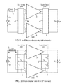
- Fig. 1 depicts an RF front-end according to the invention.
- the RF front-end (100) is adapted to receive or transmit signals located in at least two separated frequency bands comprising an input and an output and further comprising a first phase shifter (5) coupled to the input of the RF front-end (100). It further comprises a second phase shifter (6) coupled to the output of the RF front-end (100), the first phase shifter (5) being coupled to the second phase shifter (6) via a first amplifier (3) and second amplifier (4), respectively.
- the RF front-end (100) further comprising an input matching circuit (1) comprising a first input coupled to the input of the RF front-end (100) and a second input coupled to the first phase shifter (5), the first matching circuit (1) further comprising a first output coupled to an input of the first amplifier circuit (3) and a second output coupled to an input of the second amplifier circuit (4).
- the RF front-end (100) further comprises an output matching circuit (2) comprising a third input coupled to an output of the first amplifier circuit (4), and a fourth input coupled to an output of the second amplifier circuit (4).
- the first phase shifter (5) has the same structure as the second phase shifter (6), but this not necessary to be in practice. That means that the topology of the respective circuits may be identical, but not necessary the values of the respective devices used therein.
- the current invention is capable of providing amplification of signals in multiple frequency bands, without the need of switches or tunable components.
- the RF front-end can be designed such that amplification is provided in multiple frequency bands with a high degree of freedom in positioning the different operating frequencies.
- simultaneous operation in different bands is supported. This, for example, enables the design of a multi-band receiver/transmitter in which a single low noise amplifier (LNA) is used to simultaneously amplify signals in different telecommunication bands.
- LNA low noise amplifier
- a second example can be a base station power amplifier which is used to simultaneously amplify two different bands, leading to higher system efficiency and lower hardware costs.
- Yet another example could be the use in radar systems.
- phase shift of the phase shifters (5,6) is dependent on frequency.
- a frequency f 0_cm the phase shift of the phase shifter (5) at the input and the output (6) is an odd multiple of 180 degrees.
- the amplifier input voltages in both branches at the input reference plane are in-phase, causing the differential amplifier achieved with the first and second amplifiers (3,4) to operate in common mode.
- the output voltages at the output voltage reference plane are in phase.
- the phase shifter at the output (6) has a 180 degrees phase shift at this frequency, causing a differential voltage across the load impedance.
- the phase shift of the phase shifters at the input (5) and output (6) is an even multiple of 180 degrees.
- the input voltages at the input reference plane are 180 degrees out of phase, and the amplifier formed by the first and second amplifier (3,4) operates in differential mode.
- the voltages at the output reference plane also have a 180degrees phase difference and the phase shifter at the output has an insertion phase being an even multiple of 180 degrees, such that the voltage across the load has a differential component only.
- the amplifier can operate simultaneously in multiple bands, even if it does not include tunables devices or switches. Effectively this means that the differential source signal is converted to a common and differential mode signal for different frequency bands by the input matching network (1) and phase shifter (5), then it is amplified in common and differential mode by the amplifier and then converted to a differential output signal across the load by the output matching network (2) and the phase shifter at the output (6).
- phase shifters (5,6) are implemented such that the insertion phase is an odd multiple of 180 degrees at different frequencies, common-mode amplification is possible at the same frequencies, provided that the amplifier is impedance matched at these frequencies for the common mode. This can be done by designing the input and output matching networks (1,2) to provide the correct common-mode impedance transformations at these frequencies.
- the amplifier can provide gain in differential-mode at these same frequencies, provided that the differential input and output impedances are impedance matched by the matching networks at these frequencies.
- Fig. 2 shows a more detailed picture of the RF front-end. It consists of two amplifiers 3,4), an input matching network (1) for the common mode input impedance and the differential mode input impedance, an output matching network (2) for the common mode and differential mode output impedance, and two phase shifters (5,6) implemented as transmission lines.
- the phase shifters (5,6) may be implemented in several ways, for example with lumped components, passive all-pass filters, etc.
- the transmission lines (5,6) have an electrical length ⁇ 1 equal to 180 degrees at f0_cm, and an electrical length of 360 degrees at f0_dm.
- the power gain can be as in is shown in Fig. 3 .
- the differential mode input and output impedance must be matched at frequency f 0_dm .
- the first and the second of the above mentioned requirements can even be met at more than two frequencies, leading to a multiband amplifier.
- the first requirement is naturally fulfilled at multiple frequencies due to the natural phase behaviour of the transmission lines as a function of frequency.
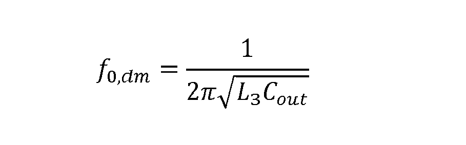
- the second requirement of having an impedance match for the common and differential mode input and output impedance is fulfilled only at f 0_cm and f 0_dm respectively. This is a consequence of the low complexity of the matching network, which are T's of inductors.
- the matching network components L1, L2, L3 and L4 in Fig.2 can be chosen by using the formulas below.
- phase shifters (5,6) and matching networks (1,2) can be implemented in several alternative ways.
- the order of complexity of the matching network can be increased to allow for multiband impedance matching.
- the matching networks (1,2) could also be implemented using distributed elements instead of lumped elements or using a combination thereof.
- the phase shifters (5,6) can be implemented in different ways. In some situations e.g. at low frequencies the use of phase shifters using lumped components can be beneficial to save area. Active phase shifters can also be used.
- phase shift is either an even or an odd multiple of 180 degrees and that the impedance matching frequency for the common mode(s) corresponds with the frequency where the phase shift of the phase shifters is an odd multiple of 180 degrees while it is an even multiple of 180 degrees at frequencie(s) where the amplifier is impedance matched for the differential mode.
- Fig. 4 depicts another embodiment of the RF front-end according to the invention. It can be seen that each of the amplifiers 3,4 can be single ended or differential as it was already shown in Figs. 1 or 2 .
- the first amplifier and the second amplifier might be transconductance amplifiers. In the very simple form the amplifiers could be a transistor made in any technology as e.g. bipolar, GaAs or, in general, a III-V compound, CMOS etc. However, depending on the application the amplifiers may be transimpedance amplifier and more general any type of controlled sources.
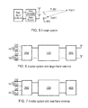
- Fig. 5 depicts a radar system using the RF front-end according to the invention.
- the embodiment refers to a low cost Multi Band Radar Transceiver.
- This system consists of a Radar Transmitter plus Receiver that is capable of emitting and receiving a series of continuous wave frequency chirps or pulses in two frequency bands F1 and F2 with frequency bandwidths BW1 and BW2.
- the transmitter and receiver blocks are connected to a radar signal controller/processor block.
- This block generates the radar pulses / chirps and derives the range, velocity and angle of multiple targets from the time of flight and phase relations of the reflected signals.
- c the speed of light
- BW the frequency bandwidth.
- Range and Frequency/Bandwidth is complex; the detection range typically decreases for higher frequency and larger bandwidth.
- Concurrent multiband operation enables a smooth frequency transition of detected targets depending upon their distance and required resolution.
- Multiband operation saves system cost by re-use of the transceiver and antenna hardware.
- Fig.6 shows an example of a Dual-Band Radar Transmitter according to this invention.
- the transmitter generates two frequency chirps at the same time: one chirp in the 76-81GHz band with a limited bandwidth of 0.5GHz for long range detection with limited resolution and another chirp in the 115-125GHz band with 5GHz bandwidth for high resolution detection with limited range.
- the signals are combined at the input of the multiband amplifier in a Signal (300) Combiner.
- the signals are split at the output of the amplifier in a Signal Splitter (200) and fed to two Single-Band antennae 400 that are each designed to radiate power in one of the target frequency bands.
- Fig.7 shows an alternative of the concept presented in Fig.6 .
- the signals at the output of the amplifier are fed into a Dual-Band antenna designed to radiate power in two frequency bands and shown together with the output splitter as block 405.
- a multiband receiver would comprise the same main building blocks as the transmitter, but in a different order.
- a Dual-Band Radar Receiver according to this invention would be able to receive two frequency chirps at the same time: one chirp in the 76-81 GHz band with a limited bandwidth of 0.5GHz for long range detection with limited resolution and another chirp in the 115-125GHz band with 5GHz bandwidth for high resolution detection with limited range.
- the signals are received by two single-band antennae and combined at the input of the multiband amplifier in a Signal Combiner.
- the signals are split at the output of the amplifier by use of a Signal Splitter and fed to two Single-Band receiver outputs for further signal processing.
- the signals are received by a Dual-Band antenna which is designed to receive power in two frequency bands this way eliminating the need for a signal combiner at the input
- the RF front-end can be used in a low cost Radar plus Point to Point Communication system as shown in Fig.8 .
- This system consists of a transmitter plus receiver that is capable of emitting and receiving a series of continuous wave frequency chirps or pulses in frequency band F1 with bandwidths BW1 and a communication signal in frequency band F2 with bandwidth BW2.
- the transmitter and receiver blocks are connected to a radar plus communication signal controller/processor block.
- This block generates the radar pulses / chirps and derives the range, velocity and angle of multiple targets from the time of flight and phase relations of the reflected signals and it generates and detects the communication signals.
- This combined Radar / Communication system offers the following advantages compared to a conventional Radar plus Communication system:
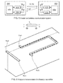
- Fig.9 depicts a layout of a transmission line, according to the invention.
- the network consists of two uncoupled single-ended transmission lines with a different electrical length.
- the connection points in the drawing of the phase shifter (5) correspond to that of the layout description. It is further remarked that the total electrical length is important for determining the phase shift but the actual geometry is less important to that.
Landscapes
- Engineering & Computer Science (AREA)
- Computer Networks & Wireless Communication (AREA)
- Signal Processing (AREA)
- Radar, Positioning & Navigation (AREA)
- Remote Sensing (AREA)
- Physics & Mathematics (AREA)
- General Physics & Mathematics (AREA)
- Amplifiers (AREA)
Abstract
- a first phase shifter (5) coupled to the input of the RF front-end (100);
- a second phase shifter (6) coupled to the output of the RF front-end (100);
- the first phase shifter (1) being coupled to the second phase shifter (2) via a first amplifier (3) and second amplifier (4), respectively.
Description
- The invention relates to a concurrent multiband receiver or transmitter or transceiver adapted to receive and/or transmit signals in more than one frequency band simultaneously.
- Modem transmitters and receivers are often required to be able to operate in different frequency bands. This can be done using different solutions.
- A first possibility is to use parallel transmitters or receivers where each transmitter/receiver is used for a specific frequency band. This is a costly solution in terms of component count, area and power consumption.
- Another possibility is to use tunable elements in the transmitter or receiver, the elements being tuned for specific frequency bands. The tunable elements can use e.g. varactors, such that the transmitter or receiver can be tuned for operation in different frequency bands as it is shown by Chong-Ru Wu et al., "A 3-5 GHz Frequency-Tunable Receiver Frontend for Multiband Applications",in IEEE MICROWAVE AND WIRELESS COMPONENTS LETTERS, VOL. 18, NO. 9, SEPTEMBER 2008. This solution requires expensive tunable components and additional digital circuitry for tuning the circuits to the correct frequency.
- Yet another alternative, which is often used to support multiband operation, is to switch between different frequency bands as it is shown by Atsushi Fukuda et al. "A High Power and Highly Efficient Multi-band Power Amplifier for Mobile Terminals" in 2010 IEEE Radio and Wireless Symposium conference publications pages 45-48. This can be done with capacitor banks and switches, or even by switching between complete matching networks. Using this alternative, additional circuitry is necessary for implementing the multiband operation.
- In another alternative, one may use wideband circuits in the transmitter or receiver. However, the maximum bandwidth of practical building blocks is naturally limited. Apart from this, for a wideband receiver there is the disadvantage of being sensitive to unwanted sources that fall within the receiver bandwidth.. In a similar way, a wideband transmitter will amplify unwanted input signals that fall within the transmitter bandwidth.
- All the previously presented alternative solutions, excepting the last one, have in common that the transmitter or receiver are capable of transmitting or receiving in only one frequency band at a time, reducing the throughput of the system as it is shown by Jussi Ryynanen et al., "Integrated Circuits for Multi-Band Multi-Mode Receivers" in the Special Issue on Wireless Reconfigurable Terminals - Part II, IEEE Circuits and Systems Magazine, second quarter 2006.
- Other alternative solutions are known from e.g.
US-A 6658265 andUS-A 6917815 . -
US-A 6658265 discloses a dual mode amplifier capable of operating in a common mode for one frequency band and a differential mode for a second frequency band. In the common mode, the amplifier provides two identical signals to a matching network, and in the differential mode, the amplifier provides two signals that are 1800 out of phase from one another to the matching network. The matching network is configured to maintain the same input and output impedance regardless of whether the amplifier is operating in the common mode or differential mode. Since the matching network operates on two signals, either common or differential, a power combining network is typically required to combine the two signals into a single signal for transmission. It is observed that the system does not support concurrent multiband operation. -
US-A 6917815 discloses an architecture for a concurrent dual band high-frequency receiver. It combines a concurrent dual-band front -end subsystem having a dual-band antenna, dual band pre-amplifier filter and concurrent dual-band LNA with an image rejection downconverter to provide the functions of a typical receiver, including reception, amplification and downconversion of a signal in two discrete desired frequency bands simultaneously. The stem disclosed here is a concurrent dualband receiver architecture but it doesn't make use of simultaneous common mode and differential mode operation. - It is therefore a need to obtain a front-end that works concurrently and provides both differential and common mode of operation with the advantage of reducing the costs and the footprint of the circuits.
- Hence, it is a need, to obtain a front-end that works in multiple frequency bands with reduced cost and footprint.
- It is therefore an object of the invention to provide an RF front-end adapted to receive or transmit signals located in at least two separated frequency bands comprising an input and an output and further comprising a first phase shifter coupled to the input of the RF front-end (100), a second phase shifter coupled to the output of the RF front-end, the first phase shifter being coupled to the second phase shifter via a first amplifier and second amplifier, respectively.
- The invention is defined by the independent claim. Dependent claims define advantageous embodiments.
- The RF front-end may further comprise an input matching circuit including a first input coupled to the input of the RF front-end and a second input coupled to the first phase shifter, the first matching circuit further comprising a first output coupled to an input of the first amplifier circuit and a second output coupled to an input of the second amplifier circuit. The RF front-end, may also comprise an output matching circuit including a third input coupled to an output of the first amplifier circuit, and a fourth input coupled to an output of the second amplifier circuit.
- In an embodiment, the first phase shifter has the same structure as the second phase shifter. The input matching circuit may have the same structure as the output matching circuit. Both the above features simplify the design of the circuit.
- The first phase shifter and the second phase shifter each comprises a delay line or a lumped passive or active filter. The choice would be dependent on the frequency range of the input signals. For lower frequencies lumped solutions might be more suitable for implementation. For higher frequencies situated in GHz range or mm range i.e. tenths or hundreds of GHz a delay line might be more suitable.
- The first phase shifter and the second phase shifter each provides at their respective outputs an odd multiple of 1800 phase shift of a signal situated in a first frequency band applied to their respective inputs.
- The first phase shifter and the second phase shifter each provides at their respective outputs an even multiple of 1800 phase shift of a signal situated in a second frequency band applied to their respective inputs.
- The input matching circuit comprises a T filter comprising inductors. The output matching circuit (2) comprises a T filter comprising inductors. Preferably, both circuits would have the same topology and probably the easiest implementation is achieved using inductors. However, it is not necessary that both circuits are identical. The choice would depend on the application where the circuit is used.
- The input matching effectuates impedance-matching between the source impedance and the common-mode input impedance of the combined amplifiers in the first frequency band, and between the source impedance and the differential mode input impedance of the combined amplifiers in the second frequency band.
- The output matching circuit provides a similar role for the output stage.
- The first amplifier and the second amplifier are single-ended or differential amplifiers. The first amplifier and the second amplifier might be transconductance amplifiers. In the very simple form the amplifiers could be a transistor made in any technology as e.g. bipolar, GaAs or, in general, a III-V compound, CMOS etc. However, depending on the application the amplifiers may be transimpedance amplifier and more general any type of controlled sources.
- In applications as radar, high frequency communications as car to car communication using IEEE 802.11/p standard or a combination thereof it is preferable to have a transmitter comprising a signal combiner coupled to an RF front-end as described above in any of the embodiments, the RF front-end being coupled to a signal splitter, the signal splitter being coupled to either a pair of single band antennae, or to a dual band antenna
- In the above application it is preferable to have a receiver comprising a signal combiner coupled to an RF front-end as described above, the RF front-end being coupled to a signal splitter, the signal combiner being coupled to either a pair of single band antenna, or to a dual band antenna.
- In an embodiment of the invention the communication devices are mounted on a vehicle as a car.
- The above and other advantages will be apparent from the exemplary description of the accompanying drawings in which
-
Fig. 1 depicts an RF front-end according to the invention; -
Fig. 2 depicts an RF front-end in more detail; -
Fig. 3 depicts the power gain of the RF front-end according to the invention; -
Fig. 4 depicts another embodiment of the RF front-end according to the invention; -
Fig. 5 depicts a radar system using the RF front-end according to the invention; -
Fig. 6 depicts a radar receiver, according to the invention; -
Fig. 7 depicts another radar receiver, according to the invention; -
Fig. 9 depicts a system comprising at least two RF front-ends, according to the invention; and - Fig. 10 depicts a layout of a transmission line, according to the invention.
-
Fig. 1 depicts an RF front-end according to the invention. The RF front-end (100) is adapted to receive or transmit signals located in at least two separated frequency bands comprising an input and an output and further comprising a first phase shifter (5) coupled to the input of the RF front-end (100). It further comprises a second phase shifter (6) coupled to the output of the RF front-end (100), the first phase shifter (5) being coupled to the second phase shifter (6) via a first amplifier (3) and second amplifier (4), respectively. - The RF front-end (100) further comprising an input matching circuit (1) comprising a first input coupled to the input of the RF front-end (100) and a second input coupled to the first phase shifter (5), the first matching circuit (1) further comprising a first output coupled to an input of the first amplifier circuit (3) and a second output coupled to an input of the second amplifier circuit (4). The RF front-end (100) further comprises an output matching circuit (2) comprising a third input coupled to an output of the first amplifier circuit (4), and a fourth input coupled to an output of the second amplifier circuit (4). Preferable, the first phase shifter (5) has the same structure as the second phase shifter (6), but this not necessary to be in practice. That means that the topology of the respective circuits may be identical, but not necessary the values of the respective devices used therein.
- The current invention is capable of providing amplification of signals in multiple frequency bands, without the need of switches or tunable components. The RF front-end can be designed such that amplification is provided in multiple frequency bands with a high degree of freedom in positioning the different operating frequencies. Also, with the present invention, simultaneous operation in different bands is supported. This, for example, enables the design of a multi-band receiver/transmitter in which a single low noise amplifier (LNA) is used to simultaneously amplify signals in different telecommunication bands. A second example can be a base station power amplifier which is used to simultaneously amplify two different bands, leading to higher system efficiency and lower hardware costs. Yet another example could be the use in radar systems.
- The phase shift of the phase shifters (5,6) is dependent on frequency. For a frequency f0_cm the phase shift of the phase shifter (5) at the input and the output (6) is an odd multiple of 180 degrees. For this frequency therefore, the amplifier input voltages in both branches at the input reference plane are in-phase, causing the differential amplifier achieved with the first and second amplifiers (3,4) to operate in common mode. For this frequency also the output voltages at the output voltage reference plane are in phase. The phase shifter at the output (6) has a 180 degrees phase shift at this frequency, causing a differential voltage across the load impedance. For a frequency f0_dm, the phase shift of the phase shifters at the input (5) and output (6) is an even multiple of 180 degrees. For this frequency therefore the input voltages at the input reference plane are 180 degrees out of phase, and the amplifier formed by the first and second amplifier (3,4) operates in differential mode. At this frequency the voltages at the output reference plane also have a 180degrees phase difference and the phase shifter at the output has an insertion phase being an even multiple of 180 degrees, such that the voltage across the load has a differential component only.
- It is observed that the amplifier can operate simultaneously in multiple bands, even if it does not include tunables devices or switches. Effectively this means that the differential source signal is converted to a common and differential mode signal for different frequency bands by the input matching network (1) and phase shifter (5), then it is amplified in common and differential mode by the amplifier and then converted to a differential output signal across the load by the output matching network (2) and the phase shifter at the output (6).
- If the phase shifters (5,6) are implemented such that the insertion phase is an odd multiple of 180 degrees at different frequencies, common-mode amplification is possible at the same frequencies, provided that the amplifier is impedance matched at these frequencies for the common mode. This can be done by designing the input and output matching networks (1,2) to provide the correct common-mode impedance transformations at these frequencies.
- If the phase shifters (5,6) have an insertion phase being an even multiple of 180 degrees at different frequencies, the amplifier can provide gain in differential-mode at these same frequencies, provided that the differential input and output impedances are impedance matched by the matching networks at these frequencies.
-
Fig. 2 shows a more detailed picture of the RF front-end. It consists of twoamplifiers 3,4), an input matching network (1) for the common mode input impedance and the differential mode input impedance, an output matching network (2) for the common mode and differential mode output impedance, and two phase shifters (5,6) implemented as transmission lines. The phase shifters (5,6) may be implemented in several ways, for example with lumped components, passive all-pass filters, etc. The transmission lines (5,6) have an electrical length β1 equal to 180 degrees at f0_cm, and an electrical length of 360 degrees at f0_dm. If in the differential mode the amplifiers' input and output impedances are matched at f0_dm and the amplifiers common mode input and output impedance is matched at f0_cm, the power gain can be as in is shown inFig. 3 . - It can be shown that two sets of requirements need to be fulfilled in order to have power gain at a frequencies f0_cm and f0_dm:
- 1. The phase shift of the phase shifters (5,6) must be an odd multiple of 180 degrees at frequency t0_cm and an even multiple of 180 degrees at frequency f0_dm;
- 2. The common mode input and output impedance must be matched at frequency f0_cm.
- The differential mode input and output impedance must be matched at frequency f0_dm.
- The first and the second of the above mentioned requirements can even be met at more than two frequencies, leading to a multiband amplifier. In this embodiment the first requirement is naturally fulfilled at multiple frequencies due to the natural phase behaviour of the transmission lines as a function of frequency. In this embodiment, the second requirement of having an impedance match for the common and differential mode input and output impedance is fulfilled only at f0_cm and f0_dm respectively. This is a consequence of the low complexity of the matching network, which are T's of inductors. The matching network components L1, L2, L3 and L4 in
Fig.2 can be chosen by using the formulas below.


- The embodiment presented above is just one of many implementation options. The phase shifters (5,6) and matching networks (1,2) can be implemented in several alternative ways. For example, the order of complexity of the matching network can be increased to allow for multiband impedance matching. The matching networks (1,2) could also be implemented using distributed elements instead of lumped elements or using a combination thereof. Also the phase shifters (5,6) can be implemented in different ways. In some situations e.g. at low frequencies the use of phase shifters using lumped components can be beneficial to save area. Active phase shifters can also be used. It is very important that the phase shift is either an even or an odd multiple of 180 degrees and that the impedance matching frequency for the common mode(s) corresponds with the frequency where the phase shift of the phase shifters is an odd multiple of 180 degrees while it is an even multiple of 180 degrees at frequencie(s) where the amplifier is impedance matched for the differential mode.
-
Fig. 4 depicts another embodiment of the RF front-end according to the invention. It can be seen that each of theamplifiers Figs. 1 or 2 . The first amplifier and the second amplifier might be transconductance amplifiers. In the very simple form the amplifiers could be a transistor made in any technology as e.g. bipolar, GaAs or, in general, a III-V compound, CMOS etc. However, depending on the application the amplifiers may be transimpedance amplifier and more general any type of controlled sources. - Even more, when they are implemented as single transistor amplifiers they may be connected as common base (gate) or emitter (source) follower, too.
-
Fig. 5 depicts a radar system using the RF front-end according to the invention. To be more precise, the embodiment refers to a low cost Multi Band Radar Transceiver. - This system consists of a Radar Transmitter plus Receiver that is capable of emitting and receiving a series of continuous wave frequency chirps or pulses in two frequency bands F1 and F2 with frequency bandwidths BW1 and BW2.
- The transmitter and receiver blocks are connected to a radar signal controller/processor block. This block generates the radar pulses / chirps and derives the range, velocity and angle of multiple targets from the time of flight and phase relations of the reflected signals.
- This Multiband Radar system offers the following advantages compared to a conventional Single band Radar system:
- The Frequency and Bandwidth may be optimized as function of the detection requirements i.e.
- Long Distance, Moderate Resolution: Low Frequency, Narrow Bandwidth.
- Short Distance, High Resolution: High Frequency, Large Bandwidth
- Resolution and Bandwidth are related according to: ΔR = c/(2.BW), wherein c is the speed of light and BW is the frequency bandwidth. The relation between Range and Frequency/Bandwidth is complex; the detection range typically decreases for higher frequency and larger bandwidth.
- Concurrent multiband operation enables a smooth frequency transition of detected targets depending upon their distance and required resolution.
- Concurrent operation in multiple frequency bands increases the rate at which information from the targets is detected and therefore decreases the response time of the system.
- Multiband operation according to this application saves system cost by re-use of the transceiver and antenna hardware.
-
Fig.6 shows an example of a Dual-Band Radar Transmitter according to this invention. The transmitter generates two frequency chirps at the same time: one chirp in the 76-81GHz band with a limited bandwidth of 0.5GHz for long range detection with limited resolution and another chirp in the 115-125GHz band with 5GHz bandwidth for high resolution detection with limited range. - The signals are combined at the input of the multiband amplifier in a Signal (300) Combiner. The signals are split at the output of the amplifier in a Signal Splitter (200) and fed to two Single-Band antennae 400 that are each designed to radiate power in one of the target frequency bands.
-
Fig.7 shows an alternative of the concept presented inFig.6 . In this case the signals at the output of the amplifier are fed into a Dual-Band antenna designed to radiate power in two frequency bands and shown together with the output splitter asblock 405. - A multiband receiver would comprise the same main building blocks as the transmitter, but in a different order. A Dual-Band Radar Receiver according to this invention would be able to receive two frequency chirps at the same time: one chirp in the 76-81 GHz band with a limited bandwidth of 0.5GHz for long range detection with limited resolution and another chirp in the 115-125GHz band with 5GHz bandwidth for high resolution detection with limited range.
- The signals are received by two single-band antennae and combined at the input of the multiband amplifier in a Signal Combiner. The signals are split at the output of the amplifier by use of a Signal Splitter and fed to two Single-Band receiver outputs for further signal processing.
Alternatively, the signals are received by a Dual-Band antenna which is designed to receive power in two frequency bands this way eliminating the need for a signal combiner at the input - In another embodiment of the invention the RF front-end can be used in a low cost Radar plus Point to Point Communication system as shown in
Fig.8 . This system consists of a transmitter plus receiver that is capable of emitting and receiving a series of continuous wave frequency chirps or pulses in frequency band F1 with bandwidths BW1 and a communication signal in frequency band F2 with bandwidth BW2. - The transmitter and receiver blocks are connected to a radar plus communication signal controller/processor block. This block generates the radar pulses / chirps and derives the range, velocity and angle of multiple targets from the time of flight and phase relations of the reflected signals and it generates and detects the communication signals.
- This combined Radar / Communication system offers the following advantages compared to a conventional Radar plus Communication system:
- It enables simultaneous detection and communication of/to objects in a particular angular direction. One example is a Car Radar / Intelligent Traffic System (ITS) Communication system in which ITS messages are exchanged using point to point communication between Cars be sending and receiving data in a specific spatial direction measured by the Radar system. This form of Spatial Re-use of the frequency spectrum avoids the problem of the limited system capacity of conventional nondirectional ITS communication systems.
- Combining Radar plus Communication functions according to this invention saves system cost by re-use of the transceiver and antenna hardware.
-
Fig.9 depicts a layout of a transmission line, according to the invention. The network consists of two uncoupled single-ended transmission lines with a different electrical length. The connection points in the drawing of the phase shifter (5) correspond to that of the layout description. It is further remarked that the total electrical length is important for determining the phase shift but the actual geometry is less important to that. - It is remarked that the scope of protection of the invention is not restricted to the embodiments described herein. Neither is the scope of protection of the invention restricted by the reference numerals in the claims. The word "comprising" does not exclude other parts than those mentioned in the claims. The word "a(n)" preceding an element does not exclude a plurality of those elements. Means forming part of the invention may both be implemented in the form of dedicated hardware or in the form of a programmed purpose processor. The invention resides in each new feature or combination of features.
Claims (19)
- An RF front-end (100) adapted to receive or transmit signals located in at least two separated frequency bands, comprising an input and an output and further comprising:- a first phase shifter (5) coupled to the input of the RF front-end (100);- a second phase shifter (6) coupled to the output of the RF front-end (100);- the first phase shifter (5) being coupled to the second phase shifter (6) via a first amplifier (3) and second amplifier (4), respectively.
- An RF front-end (100) as claimed in claim 1, further comprising an input matching circuit (1) comprising a first input coupled to the input of the RF front-end (100) and a second input coupled to the first phase shifter (5), the first matching circuit (1) further comprising a first output coupled to an input of the first amplifier circuit (3) and a second output coupled to an input of the second amplifier circuit (4).
- An RF front-end (100) as claimed in claim 1 or 2, further comprising an output matching circuit (2) comprising a third input coupled to an output of the first amplifier circuit (3), and a fourth input coupled to an output of the second amplifier circuit (4).
- An RF front-end (100) as claimed in any of the claims 1to 3, wherein the first phase shifter (1) has the same structure as the second phase shifter (2).
- An RF front-end (100) as claimed in any of the claims 1 to 4, wherein the input matching circuit (1) has the same structure as the output matching circuit (2).
- An RF front-end (100) as claimed in any of the claims 1 to 5, wherein the first phase shifter (5) and the second phase shifter (6) each comprises a delay line or a lumped passive or active filter.
- An RF front-end (100) as claimed in any of the claims 1 to 6, wherein the first phase shifter (5) and the second phase shifter (6) each provides at their respective outputs an odd multiple of 1800 phase shift of a signal situated in a first frequency band applied to their respective inputs.
- An RF front-end (100) as claimed in any of the claims 1 to 7, wherein the first phase shifter (5) and the second phase shifter (6) each provides at their respective outputs an even multiple of 1800 phase shift of a signal situated in a second frequency band applied to their respective inputs.
- An RF front-end (100) as claimed in any of the claims 1 to 8, wherein the input (1) matching circuit comprises a T filter comprising inductors.
- An RF front-end (100) as claimed in any of the claims 1 to 9, wherein the output matching circuit (2) comprises a T filter comprising inductors.
- An RF front-end (100) as claimed in any of the claims 1 to 10, wherein the first amplifier (3) and the second amplifier (4) are single-ended or differential amplifiers.
- An RF front-end (100) as claimed in any of the claims 1 to 11, wherein the first amplifier (3) and the second amplifier (4) are transconductace amplifiers.
- An RF front-end (100) as claimed in any of the claims 1 to 12, wherein the first amplifier (3) and the second amplifier (4) are transistors amplifiers.
- A transmitter comprising a signal combiner (200) coupled to an RF front-end (100) as claimed in any of the preceding claims, the RF front-end (100) being coupled to a signal splitter (300), the signal splitter being coupled to either a pair of single band antenna (400), or to a dual band antenna (405).
- A receiver comprising a signal combiner (200) coupled to an RF front-end (100) as claimed in claims 1 to 13, the RF front-end (100) being coupled to a signal splitter (300), the signal combiner (200) being coupled to either a pair of single band antenna (400), or to a dual band antenna (405).
- A communication system comprising at least a pair of communication devices each comprising a transmitter as claimed in claim 14 and a receiver as claimed in claim 15.
- A radar system comprising a transmitter as claimed in claim 14 and/or a receiver as claimed in claim 15.
- A car comprising a radar system as claimed in claim 17.
- A communication system comprising at least a pair of communication devices as claimed in claim 16, each of the communication devices being mounted on a respective car.
Priority Applications (3)
| Application Number | Priority Date | Filing Date | Title |
|---|---|---|---|
| EP12195634.6A EP2741422B1 (en) | 2012-12-05 | 2012-12-05 | A concurrent multiband transceiver |
| CN201310578802.6A CN103856234B (en) | 2012-12-05 | 2013-11-18 | Concurrent multiband transceivers |
| US14/097,073 US9329259B2 (en) | 2012-12-05 | 2013-12-04 | Concurrent multiband transceiver |
Applications Claiming Priority (1)
| Application Number | Priority Date | Filing Date | Title |
|---|---|---|---|
| EP12195634.6A EP2741422B1 (en) | 2012-12-05 | 2012-12-05 | A concurrent multiband transceiver |
Publications (2)
| Publication Number | Publication Date |
|---|---|
| EP2741422A1 true EP2741422A1 (en) | 2014-06-11 |
| EP2741422B1 EP2741422B1 (en) | 2015-07-01 |
Family
ID=47458655
Family Applications (1)
| Application Number | Title | Priority Date | Filing Date |
|---|---|---|---|
| EP12195634.6A Active EP2741422B1 (en) | 2012-12-05 | 2012-12-05 | A concurrent multiband transceiver |
Country Status (3)
| Country | Link |
|---|---|
| US (1) | US9329259B2 (en) |
| EP (1) | EP2741422B1 (en) |
| CN (1) | CN103856234B (en) |
Cited By (2)
| Publication number | Priority date | Publication date | Assignee | Title |
|---|---|---|---|---|
| US20160211805A1 (en) * | 2013-09-09 | 2016-07-21 | Nec Corporation | Power amplification device and control method of power amplification device |
| EP3367119A1 (en) * | 2017-02-27 | 2018-08-29 | Nxp B.V. | Radar |
Families Citing this family (12)
| Publication number | Priority date | Publication date | Assignee | Title |
|---|---|---|---|---|
| EP2741422B1 (en) | 2012-12-05 | 2015-07-01 | Nxp B.V. | A concurrent multiband transceiver |
| EP2741424A1 (en) * | 2012-12-05 | 2014-06-11 | Nxp B.V. | A concurrent multiband transceiver |
| WO2014094050A1 (en) * | 2012-12-20 | 2014-06-26 | The University Of Melbourne | A receiver circuit |
| US9548767B2 (en) | 2014-11-04 | 2017-01-17 | Qualcomm Incorporated | Multi-band amplifier |
| US9654310B1 (en) * | 2016-11-19 | 2017-05-16 | Nxp Usa, Inc. | Analog delay cell and tapped delay line comprising the analog delay cell |
| CN106899271B (en) * | 2017-01-10 | 2020-03-31 | 锐迪科微电子(上海)有限公司 | Complementary power amplifier |
| US10268207B2 (en) * | 2017-03-10 | 2019-04-23 | Ford Global Technologies, Llc | Autonomous vehicle network bandwidth bridging |
| US10948585B1 (en) * | 2018-04-05 | 2021-03-16 | Rockwell Collins, Inc. | Dual band radar altimeter system and method |
| KR102581317B1 (en) * | 2018-12-24 | 2023-09-22 | 삼성전자 주식회사 | An electronic device including a plurality of antenna arrays |
| CN109529547A (en) | 2018-12-24 | 2019-03-29 | 大连理工大学 | The decarbonizing solution of the trapping carbon dioxide in gas mixture of hygroscopicity influence can be reduced |
| CN113376622B (en) * | 2021-04-29 | 2022-04-26 | 中国科学院空天信息创新研究院 | Millimeter wave phased array radar with low link loss and detection method thereof |
| CN117335822B (en) * | 2023-11-30 | 2024-02-23 | 上海安其威微电子科技有限公司 | Radio frequency front end receiving circuit, phased array antenna circuit and chip |
Citations (3)
| Publication number | Priority date | Publication date | Assignee | Title |
|---|---|---|---|---|
| US6658265B1 (en) | 2000-04-25 | 2003-12-02 | Rf Micro Devices, Inc. | Matching network for a dual mode RF amplifier |
| US6917815B2 (en) | 2001-03-14 | 2005-07-12 | California Institute Of Technology | Concurrent dual-band receiver architecture |
| WO2011026522A1 (en) * | 2009-09-04 | 2011-03-10 | Laird Technologies Ab | An antenna device and a portable radio communication device comprising such antenna device |
Family Cites Families (15)
| Publication number | Priority date | Publication date | Assignee | Title |
|---|---|---|---|---|
| US3740748A (en) * | 1968-05-31 | 1973-06-19 | Hughes Aircraft Co | Electronic image cancellation for doppler receivers |
| KR20030002452A (en) * | 2001-06-29 | 2003-01-09 | 엘지전자 주식회사 | Triple band embodiment circuit in mobile phone |
| US7190933B2 (en) * | 2002-11-01 | 2007-03-13 | Intergration Associates Inc. | Method and apparatus for automatic tuning of a resonant loop antenna in a transceiver circuit |
| US6990357B2 (en) | 2003-10-17 | 2006-01-24 | Nokia Corporation | Front-end arrangements for multiband multimode communication engines |
| US7555276B2 (en) | 2005-12-19 | 2009-06-30 | Sony Ericsson Mobile Communications Ab | Devices, methods, and computer program products for controlling power transfer to an antenna in a wireless mobile terminal |
| US20070155350A1 (en) | 2005-12-29 | 2007-07-05 | Wionics Research | Method of frequency planning in an ultra wide band system |
| US8447348B2 (en) * | 2006-09-27 | 2013-05-21 | Broadcom Corporation | Configurable antenna structure and applications thereof |
| KR101547818B1 (en) * | 2008-01-29 | 2015-08-27 | 삼성전자주식회사 | In a time division duplex radio communication system, a transmitting / |
| WO2009113307A1 (en) * | 2008-03-13 | 2009-09-17 | パナソニック株式会社 | Signal branching filter, electronic device using the same, antenna apparatus, and signal transmission system used in all of the above |
| US7733265B2 (en) * | 2008-04-04 | 2010-06-08 | Toyota Motor Engineering & Manufacturing North America, Inc. | Three dimensional integrated automotive radars and methods of manufacturing the same |
| CN102096079B (en) | 2009-12-12 | 2013-12-11 | 杭州中科微电子有限公司 | Method for constructing radio frequency front end of multi-mode multi-band satellite navigation receiver and module thereof |
| CN102414996B (en) | 2010-03-02 | 2014-04-09 | 松下电器产业株式会社 | Wireless communication device and wireless communication method |
| US8626084B2 (en) * | 2010-05-13 | 2014-01-07 | Qualcomm, Incorporated | Area efficient concurrent matching transceiver |
| US8599726B2 (en) * | 2010-06-03 | 2013-12-03 | Broadcom Corporation | Front end module with a tunable balancing network |
| EP2741422B1 (en) | 2012-12-05 | 2015-07-01 | Nxp B.V. | A concurrent multiband transceiver |
-
2012
- 2012-12-05 EP EP12195634.6A patent/EP2741422B1/en active Active
-
2013
- 2013-11-18 CN CN201310578802.6A patent/CN103856234B/en active Active
- 2013-12-04 US US14/097,073 patent/US9329259B2/en active Active
Patent Citations (3)
| Publication number | Priority date | Publication date | Assignee | Title |
|---|---|---|---|---|
| US6658265B1 (en) | 2000-04-25 | 2003-12-02 | Rf Micro Devices, Inc. | Matching network for a dual mode RF amplifier |
| US6917815B2 (en) | 2001-03-14 | 2005-07-12 | California Institute Of Technology | Concurrent dual-band receiver architecture |
| WO2011026522A1 (en) * | 2009-09-04 | 2011-03-10 | Laird Technologies Ab | An antenna device and a portable radio communication device comprising such antenna device |
Non-Patent Citations (5)
| Title |
|---|
| ATSUSHI FUKUDA ET AL.: "A High Power and Highly Efficient Multi-band Power Amplifier for Mobile Terminals", IEEE RADIO AND WIRELESS SYMPOSIUM CONFERENCE PUBLICATIONS, 2010, pages 45 - 48, XP031650214 |
| CHONG-RU WU ET AL.: "A 3-5 GHz Frequency-Tunable Receiver Frontend for Multiband Applications", IEEE MICROWAVE AND WIRELESS COMPONENTS LETTERS, vol. 18, no. 9, September 2008 (2008-09-01), XP011234488, DOI: doi:10.1109/LMWC.2008.2002491 |
| DAVID E MEHARRY ET AL: "Broad Bandwidth Transformer Coupled Differential Amplifiers for High Dynamic Range", IEEE JOURNAL OF SOLID-STATE CIRCUITS, IEEE SERVICE CENTER, PISCATAWAY, NJ, USA, vol. 34, no. 9, 1 September 1999 (1999-09-01), XP011061078, ISSN: 0018-9200 * |
| FATEMEH TAGHIAN ET AL: "Design and nonlinear analysis of a dual-band Doherty power amplifier for ISM and LMDS applications", APPLIED ELECTROMAGNETICS CONFERENCE (AEMC), 2011 IEEE, IEEE, 18 December 2011 (2011-12-18), pages 1 - 4, XP032215205, ISBN: 978-1-4577-1098-8, DOI: 10.1109/AEMC.2011.6256883 * |
| JUSSI RYYNANEN ET AL.: "Integrated Circuits for Multi-Band Multi-Mode Receivers", IEEE CIRCUITS AND SYSTEMS MAGAZINE, 2006 |
Cited By (3)
| Publication number | Priority date | Publication date | Assignee | Title |
|---|---|---|---|---|
| US20160211805A1 (en) * | 2013-09-09 | 2016-07-21 | Nec Corporation | Power amplification device and control method of power amplification device |
| US9673760B2 (en) * | 2013-09-09 | 2017-06-06 | Nec Corporation | Power amplification device and control method of power amplification device |
| EP3367119A1 (en) * | 2017-02-27 | 2018-08-29 | Nxp B.V. | Radar |
Also Published As
| Publication number | Publication date |
|---|---|
| US9329259B2 (en) | 2016-05-03 |
| EP2741422B1 (en) | 2015-07-01 |
| US20140159935A1 (en) | 2014-06-12 |
| CN103856234A (en) | 2014-06-11 |
| CN103856234B (en) | 2016-01-06 |
Similar Documents
| Publication | Publication Date | Title |
|---|---|---|
| EP2741422B1 (en) | A concurrent multiband transceiver | |
| US9106314B2 (en) | Concurrent multiband transceiver | |
| US9473195B2 (en) | Phase-arrayed transceiver | |
| US9413416B2 (en) | Transmit and receive RF multiplexer | |
| US8742981B2 (en) | Microstrip coupler combining transmit-receive signal separation and differential to single ended conversion | |
| US7538719B2 (en) | Mixer circuit and radar transceiver | |
| US11239873B2 (en) | Front-end circuit and communication device | |
| US10547345B2 (en) | Radio-frequency transceiver front-end circuit | |
| JP2015208007A5 (en) | ||
| US10873122B2 (en) | Communication device | |
| US11750253B2 (en) | Multi-band transmitter | |
| JPH09116458A (en) | Multi-band high frequency circuit for mobile radio | |
| US20230336203A1 (en) | Transformer-based current-reuse amplifier with embedded iq generation for compact image rejection architecture in multi-band millimeter-wave 5g communication | |
| US9606221B2 (en) | Circuit arrangement for a front end of an FMCW radar transceiver, FMCW radar transceiver and method for operation | |
| US11336237B2 (en) | Vector modulator for millimeter wave applications | |
| CN111541431A (en) | Radio frequency front end circuit, radio frequency front end device and system of millimeter waves and terahertz waves | |
| US20210351506A1 (en) | Ultra-small millimeter wave 5g beam former architecture | |
| CN110940969B (en) | A digital T/R module for multi-beam DBF phased array system | |
| US9780943B2 (en) | Broadband distributed amplifier based active duplexer | |
| CN113472299B (en) | Signal receiving and transmitting front-end circuit | |
| CN110995290A (en) | Wideband radio frequency transceiver architecture supporting UWB and FMCW dual modes |
Legal Events
| Date | Code | Title | Description |
|---|---|---|---|
| PUAI | Public reference made under article 153(3) epc to a published international application that has entered the european phase |
Free format text: ORIGINAL CODE: 0009012 |
|
| 17P | Request for examination filed |
Effective date: 20131031 |
|
| AK | Designated contracting states |
Kind code of ref document: A1 Designated state(s): AL AT BE BG CH CY CZ DE DK EE ES FI FR GB GR HR HU IE IS IT LI LT LU LV MC MK MT NL NO PL PT RO RS SE SI SK SM TR |
|
| AX | Request for extension of the european patent |
Extension state: BA ME |
|
| GRAP | Despatch of communication of intention to grant a patent |
Free format text: ORIGINAL CODE: EPIDOSNIGR1 |
|
| RIC1 | Information provided on ipc code assigned before grant |
Ipc: H04B 1/18 20060101ALI20140829BHEP Ipc: G01S 13/02 20060101ALI20140829BHEP Ipc: G01S 7/03 20060101ALI20140829BHEP Ipc: H04B 1/00 20060101AFI20140829BHEP |
|
| INTG | Intention to grant announced |
Effective date: 20140923 |
|
| RBV | Designated contracting states (corrected) |
Designated state(s): AL AT BE BG CH CY CZ DE DK EE ES FI FR GB GR HR HU IE IS IT LI LT LU LV MC MK MT NL NO PL PT RO RS SE SI SK SM TR |
|
| GRAP | Despatch of communication of intention to grant a patent |
Free format text: ORIGINAL CODE: EPIDOSNIGR1 |
|
| GRAJ | Information related to disapproval of communication of intention to grant by the applicant or resumption of examination proceedings by the epo deleted |
Free format text: ORIGINAL CODE: EPIDOSDIGR1 |
|
| GRAP | Despatch of communication of intention to grant a patent |
Free format text: ORIGINAL CODE: EPIDOSNIGR1 |
|
| RIC1 | Information provided on ipc code assigned before grant |
Ipc: G01S 13/93 20060101ALI20150209BHEP Ipc: G01S 13/02 20060101ALI20150209BHEP Ipc: H04B 1/18 20060101ALI20150209BHEP Ipc: G01S 7/00 20060101ALI20150209BHEP Ipc: H04B 1/00 20060101AFI20150209BHEP Ipc: G01S 7/03 20060101ALI20150209BHEP |
|
| INTG | Intention to grant announced |
Effective date: 20150225 |
|
| INTG | Intention to grant announced |
Effective date: 20150310 |
|
| GRAS | Grant fee paid |
Free format text: ORIGINAL CODE: EPIDOSNIGR3 |
|
| GRAA | (expected) grant |
Free format text: ORIGINAL CODE: 0009210 |
|
| AK | Designated contracting states |
Kind code of ref document: B1 Designated state(s): AL AT BE BG CH CY CZ DE DK EE ES FI FR GB GR HR HU IE IS IT LI LT LU LV MC MK MT NL NO PL PT RO RS SE SI SK SM TR |
|
| REG | Reference to a national code |
Ref country code: GB Ref legal event code: FG4D |
|
| REG | Reference to a national code |
Ref country code: AT Ref legal event code: REF Ref document number: 734486 Country of ref document: AT Kind code of ref document: T Effective date: 20150715 Ref country code: CH Ref legal event code: EP |
|
| REG | Reference to a national code |
Ref country code: IE Ref legal event code: FG4D |
|
| REG | Reference to a national code |
Ref country code: DE Ref legal event code: R096 Ref document number: 602012008350 Country of ref document: DE |
|
| REG | Reference to a national code |
Ref country code: AT Ref legal event code: MK05 Ref document number: 734486 Country of ref document: AT Kind code of ref document: T Effective date: 20150701 |
|
| REG | Reference to a national code |
Ref country code: FR Ref legal event code: PLFP Year of fee payment: 4 |
|
| REG | Reference to a national code |
Ref country code: NL Ref legal event code: MP Effective date: 20150701 |
|
| REG | Reference to a national code |
Ref country code: LT Ref legal event code: MG4D |
|
| PG25 | Lapsed in a contracting state [announced via postgrant information from national office to epo] |
Ref country code: NO Free format text: LAPSE BECAUSE OF FAILURE TO SUBMIT A TRANSLATION OF THE DESCRIPTION OR TO PAY THE FEE WITHIN THE PRESCRIBED TIME-LIMIT Effective date: 20151001 Ref country code: FI Free format text: LAPSE BECAUSE OF FAILURE TO SUBMIT A TRANSLATION OF THE DESCRIPTION OR TO PAY THE FEE WITHIN THE PRESCRIBED TIME-LIMIT Effective date: 20150701 Ref country code: GR Free format text: LAPSE BECAUSE OF FAILURE TO SUBMIT A TRANSLATION OF THE DESCRIPTION OR TO PAY THE FEE WITHIN THE PRESCRIBED TIME-LIMIT Effective date: 20151002 Ref country code: LV Free format text: LAPSE BECAUSE OF FAILURE TO SUBMIT A TRANSLATION OF THE DESCRIPTION OR TO PAY THE FEE WITHIN THE PRESCRIBED TIME-LIMIT Effective date: 20150701 Ref country code: LT Free format text: LAPSE BECAUSE OF FAILURE TO SUBMIT A TRANSLATION OF THE DESCRIPTION OR TO PAY THE FEE WITHIN THE PRESCRIBED TIME-LIMIT Effective date: 20150701 |
|
| PG25 | Lapsed in a contracting state [announced via postgrant information from national office to epo] |
Ref country code: PL Free format text: LAPSE BECAUSE OF FAILURE TO SUBMIT A TRANSLATION OF THE DESCRIPTION OR TO PAY THE FEE WITHIN THE PRESCRIBED TIME-LIMIT Effective date: 20150701 Ref country code: SE Free format text: LAPSE BECAUSE OF FAILURE TO SUBMIT A TRANSLATION OF THE DESCRIPTION OR TO PAY THE FEE WITHIN THE PRESCRIBED TIME-LIMIT Effective date: 20150701 Ref country code: PT Free format text: LAPSE BECAUSE OF FAILURE TO SUBMIT A TRANSLATION OF THE DESCRIPTION OR TO PAY THE FEE WITHIN THE PRESCRIBED TIME-LIMIT Effective date: 20151102 Ref country code: HR Free format text: LAPSE BECAUSE OF FAILURE TO SUBMIT A TRANSLATION OF THE DESCRIPTION OR TO PAY THE FEE WITHIN THE PRESCRIBED TIME-LIMIT Effective date: 20150701 Ref country code: AT Free format text: LAPSE BECAUSE OF FAILURE TO SUBMIT A TRANSLATION OF THE DESCRIPTION OR TO PAY THE FEE WITHIN THE PRESCRIBED TIME-LIMIT Effective date: 20150701 Ref country code: RS Free format text: LAPSE BECAUSE OF FAILURE TO SUBMIT A TRANSLATION OF THE DESCRIPTION OR TO PAY THE FEE WITHIN THE PRESCRIBED TIME-LIMIT Effective date: 20150701 Ref country code: IS Free format text: LAPSE BECAUSE OF FAILURE TO SUBMIT A TRANSLATION OF THE DESCRIPTION OR TO PAY THE FEE WITHIN THE PRESCRIBED TIME-LIMIT Effective date: 20151101 Ref country code: ES Free format text: LAPSE BECAUSE OF FAILURE TO SUBMIT A TRANSLATION OF THE DESCRIPTION OR TO PAY THE FEE WITHIN THE PRESCRIBED TIME-LIMIT Effective date: 20150701 |
|
| REG | Reference to a national code |
Ref country code: DE Ref legal event code: R097 Ref document number: 602012008350 Country of ref document: DE |
|
| PG25 | Lapsed in a contracting state [announced via postgrant information from national office to epo] |
Ref country code: DK Free format text: LAPSE BECAUSE OF FAILURE TO SUBMIT A TRANSLATION OF THE DESCRIPTION OR TO PAY THE FEE WITHIN THE PRESCRIBED TIME-LIMIT Effective date: 20150701 Ref country code: SK Free format text: LAPSE BECAUSE OF FAILURE TO SUBMIT A TRANSLATION OF THE DESCRIPTION OR TO PAY THE FEE WITHIN THE PRESCRIBED TIME-LIMIT Effective date: 20150701 Ref country code: CZ Free format text: LAPSE BECAUSE OF FAILURE TO SUBMIT A TRANSLATION OF THE DESCRIPTION OR TO PAY THE FEE WITHIN THE PRESCRIBED TIME-LIMIT Effective date: 20150701 Ref country code: EE Free format text: LAPSE BECAUSE OF FAILURE TO SUBMIT A TRANSLATION OF THE DESCRIPTION OR TO PAY THE FEE WITHIN THE PRESCRIBED TIME-LIMIT Effective date: 20150701 Ref country code: IT Free format text: LAPSE BECAUSE OF FAILURE TO SUBMIT A TRANSLATION OF THE DESCRIPTION OR TO PAY THE FEE WITHIN THE PRESCRIBED TIME-LIMIT Effective date: 20150701 |
|
| PLBE | No opposition filed within time limit |
Free format text: ORIGINAL CODE: 0009261 |
|
| STAA | Information on the status of an ep patent application or granted ep patent |
Free format text: STATUS: NO OPPOSITION FILED WITHIN TIME LIMIT |
|
| PG25 | Lapsed in a contracting state [announced via postgrant information from national office to epo] |
Ref country code: RO Free format text: LAPSE BECAUSE OF FAILURE TO SUBMIT A TRANSLATION OF THE DESCRIPTION OR TO PAY THE FEE WITHIN THE PRESCRIBED TIME-LIMIT Effective date: 20150701 Ref country code: BE Free format text: LAPSE BECAUSE OF NON-PAYMENT OF DUE FEES Effective date: 20151231 |
|
| 26N | No opposition filed |
Effective date: 20160404 |
|
| PG25 | Lapsed in a contracting state [announced via postgrant information from national office to epo] |
Ref country code: LU Free format text: LAPSE BECAUSE OF FAILURE TO SUBMIT A TRANSLATION OF THE DESCRIPTION OR TO PAY THE FEE WITHIN THE PRESCRIBED TIME-LIMIT Effective date: 20151205 Ref country code: MC Free format text: LAPSE BECAUSE OF FAILURE TO SUBMIT A TRANSLATION OF THE DESCRIPTION OR TO PAY THE FEE WITHIN THE PRESCRIBED TIME-LIMIT Effective date: 20150701 |
|
| REG | Reference to a national code |
Ref country code: CH Ref legal event code: PL |
|
| PG25 | Lapsed in a contracting state [announced via postgrant information from national office to epo] |
Ref country code: SI Free format text: LAPSE BECAUSE OF FAILURE TO SUBMIT A TRANSLATION OF THE DESCRIPTION OR TO PAY THE FEE WITHIN THE PRESCRIBED TIME-LIMIT Effective date: 20150701 |
|
| REG | Reference to a national code |
Ref country code: IE Ref legal event code: MM4A |
|
| PG25 | Lapsed in a contracting state [announced via postgrant information from national office to epo] |
Ref country code: LI Free format text: LAPSE BECAUSE OF NON-PAYMENT OF DUE FEES Effective date: 20151231 Ref country code: IE Free format text: LAPSE BECAUSE OF NON-PAYMENT OF DUE FEES Effective date: 20151205 Ref country code: CH Free format text: LAPSE BECAUSE OF NON-PAYMENT OF DUE FEES Effective date: 20151231 |
|
| REG | Reference to a national code |
Ref country code: FR Ref legal event code: PLFP Year of fee payment: 5 |
|
| PG25 | Lapsed in a contracting state [announced via postgrant information from national office to epo] |
Ref country code: BE Free format text: LAPSE BECAUSE OF FAILURE TO SUBMIT A TRANSLATION OF THE DESCRIPTION OR TO PAY THE FEE WITHIN THE PRESCRIBED TIME-LIMIT Effective date: 20150701 |
|
| PG25 | Lapsed in a contracting state [announced via postgrant information from national office to epo] |
Ref country code: HU Free format text: LAPSE BECAUSE OF FAILURE TO SUBMIT A TRANSLATION OF THE DESCRIPTION OR TO PAY THE FEE WITHIN THE PRESCRIBED TIME-LIMIT; INVALID AB INITIO Effective date: 20121205 Ref country code: BG Free format text: LAPSE BECAUSE OF FAILURE TO SUBMIT A TRANSLATION OF THE DESCRIPTION OR TO PAY THE FEE WITHIN THE PRESCRIBED TIME-LIMIT Effective date: 20150701 Ref country code: SM Free format text: LAPSE BECAUSE OF FAILURE TO SUBMIT A TRANSLATION OF THE DESCRIPTION OR TO PAY THE FEE WITHIN THE PRESCRIBED TIME-LIMIT Effective date: 20150701 |
|
| PG25 | Lapsed in a contracting state [announced via postgrant information from national office to epo] |
Ref country code: NL Free format text: LAPSE BECAUSE OF FAILURE TO SUBMIT A TRANSLATION OF THE DESCRIPTION OR TO PAY THE FEE WITHIN THE PRESCRIBED TIME-LIMIT Effective date: 20150701 Ref country code: CY Free format text: LAPSE BECAUSE OF FAILURE TO SUBMIT A TRANSLATION OF THE DESCRIPTION OR TO PAY THE FEE WITHIN THE PRESCRIBED TIME-LIMIT Effective date: 20150701 |
|
| PG25 | Lapsed in a contracting state [announced via postgrant information from national office to epo] |
Ref country code: MT Free format text: LAPSE BECAUSE OF FAILURE TO SUBMIT A TRANSLATION OF THE DESCRIPTION OR TO PAY THE FEE WITHIN THE PRESCRIBED TIME-LIMIT Effective date: 20150701 |
|
| REG | Reference to a national code |
Ref country code: FR Ref legal event code: PLFP Year of fee payment: 6 |
|
| PG25 | Lapsed in a contracting state [announced via postgrant information from national office to epo] |
Ref country code: MK Free format text: LAPSE BECAUSE OF FAILURE TO SUBMIT A TRANSLATION OF THE DESCRIPTION OR TO PAY THE FEE WITHIN THE PRESCRIBED TIME-LIMIT Effective date: 20150701 |
|
| PG25 | Lapsed in a contracting state [announced via postgrant information from national office to epo] |
Ref country code: AL Free format text: LAPSE BECAUSE OF FAILURE TO SUBMIT A TRANSLATION OF THE DESCRIPTION OR TO PAY THE FEE WITHIN THE PRESCRIBED TIME-LIMIT Effective date: 20150701 Ref country code: TR Free format text: LAPSE BECAUSE OF FAILURE TO SUBMIT A TRANSLATION OF THE DESCRIPTION OR TO PAY THE FEE WITHIN THE PRESCRIBED TIME-LIMIT Effective date: 20150701 |
|
| P01 | Opt-out of the competence of the unified patent court (upc) registered |
Effective date: 20230725 |
|
| PGFP | Annual fee paid to national office [announced via postgrant information from national office to epo] |
Ref country code: DE Payment date: 20251126 Year of fee payment: 14 |
|
| PGFP | Annual fee paid to national office [announced via postgrant information from national office to epo] |
Ref country code: GB Payment date: 20251119 Year of fee payment: 14 |
|
| PGFP | Annual fee paid to national office [announced via postgrant information from national office to epo] |
Ref country code: FR Payment date: 20251120 Year of fee payment: 14 |