EP2741366A1 - Antenna device, and communication terminal device - Google Patents
Antenna device, and communication terminal device Download PDFInfo
- Publication number
- EP2741366A1 EP2741366A1 EP13831926.4A EP13831926A EP2741366A1 EP 2741366 A1 EP2741366 A1 EP 2741366A1 EP 13831926 A EP13831926 A EP 13831926A EP 2741366 A1 EP2741366 A1 EP 2741366A1
- Authority
- EP
- European Patent Office
- Prior art keywords
- mode
- conductor
- resonance
- inductance element
- power feed
- Prior art date
- Legal status (The legal status is an assumption and is not a legal conclusion. Google has not performed a legal analysis and makes no representation as to the accuracy of the status listed.)
- Withdrawn
Links
- 238000004891 communication Methods 0.000 title claims description 16
- 230000005855 radiation Effects 0.000 claims abstract description 53
- 239000004020 conductor Substances 0.000 claims description 69
- 239000000463 material Substances 0.000 claims description 28
- 239000010410 layer Substances 0.000 description 29
- 238000010586 diagram Methods 0.000 description 7
- 230000005684 electric field Effects 0.000 description 6
- 239000000919 ceramic Substances 0.000 description 3
- 230000001747 exhibiting effect Effects 0.000 description 3
- 229920005989 resin Polymers 0.000 description 3
- 239000011347 resin Substances 0.000 description 3
- 230000005540 biological transmission Effects 0.000 description 2
- 230000010267 cellular communication Effects 0.000 description 2
- 230000008878 coupling Effects 0.000 description 2
- 238000010168 coupling process Methods 0.000 description 2
- 238000005859 coupling reaction Methods 0.000 description 2
- RYGMFSIKBFXOCR-UHFFFAOYSA-N Copper Chemical compound [Cu] RYGMFSIKBFXOCR-UHFFFAOYSA-N 0.000 description 1
- 239000000654 additive Substances 0.000 description 1
- 230000000996 additive effect Effects 0.000 description 1
- 229910052802 copper Inorganic materials 0.000 description 1
- 239000010949 copper Substances 0.000 description 1
- 230000000694 effects Effects 0.000 description 1
- 239000011229 interlayer Substances 0.000 description 1
- 239000004973 liquid crystal related substance Substances 0.000 description 1
- 239000007769 metal material Substances 0.000 description 1
- 238000000034 method Methods 0.000 description 1
- 238000010295 mobile communication Methods 0.000 description 1
- 230000005404 monopole Effects 0.000 description 1
- 229910052709 silver Inorganic materials 0.000 description 1
- 239000004332 silver Substances 0.000 description 1
- 239000000758 substrate Substances 0.000 description 1
- 229920005992 thermoplastic resin Polymers 0.000 description 1
- 229920001187 thermosetting polymer Polymers 0.000 description 1
- 238000004804 winding Methods 0.000 description 1
Images



Classifications
-
- H—ELECTRICITY
- H01—ELECTRIC ELEMENTS
- H01Q—ANTENNAS, i.e. RADIO AERIALS
- H01Q1/00—Details of, or arrangements associated with, antennas
- H01Q1/50—Structural association of antennas with earthing switches, lead-in devices or lightning protectors
-
- H—ELECTRICITY
- H01—ELECTRIC ELEMENTS
- H01Q—ANTENNAS, i.e. RADIO AERIALS
- H01Q7/00—Loop antennas with a substantially uniform current distribution around the loop and having a directional radiation pattern in a plane perpendicular to the plane of the loop
-
- H—ELECTRICITY
- H01—ELECTRIC ELEMENTS
- H01Q—ANTENNAS, i.e. RADIO AERIALS
- H01Q1/00—Details of, or arrangements associated with, antennas
- H01Q1/12—Supports; Mounting means
- H01Q1/22—Supports; Mounting means by structural association with other equipment or articles
- H01Q1/24—Supports; Mounting means by structural association with other equipment or articles with receiving set
- H01Q1/241—Supports; Mounting means by structural association with other equipment or articles with receiving set used in mobile communications, e.g. GSM
- H01Q1/242—Supports; Mounting means by structural association with other equipment or articles with receiving set used in mobile communications, e.g. GSM specially adapted for hand-held use
- H01Q1/243—Supports; Mounting means by structural association with other equipment or articles with receiving set used in mobile communications, e.g. GSM specially adapted for hand-held use with built-in antennas
-
- H—ELECTRICITY
- H01—ELECTRIC ELEMENTS
- H01Q—ANTENNAS, i.e. RADIO AERIALS
- H01Q5/00—Arrangements for simultaneous operation of antennas on two or more different wavebands, e.g. dual-band or multi-band arrangements
- H01Q5/30—Arrangements for providing operation on different wavebands
- H01Q5/307—Individual or coupled radiating elements, each element being fed in an unspecified way
- H01Q5/314—Individual or coupled radiating elements, each element being fed in an unspecified way using frequency dependent circuits or components, e.g. trap circuits or capacitors
- H01Q5/335—Individual or coupled radiating elements, each element being fed in an unspecified way using frequency dependent circuits or components, e.g. trap circuits or capacitors at the feed, e.g. for impedance matching
-
- H—ELECTRICITY
- H01—ELECTRIC ELEMENTS
- H01Q—ANTENNAS, i.e. RADIO AERIALS
- H01Q5/00—Arrangements for simultaneous operation of antennas on two or more different wavebands, e.g. dual-band or multi-band arrangements
- H01Q5/30—Arrangements for providing operation on different wavebands
- H01Q5/307—Individual or coupled radiating elements, each element being fed in an unspecified way
- H01Q5/342—Individual or coupled radiating elements, each element being fed in an unspecified way for different propagation modes
- H01Q5/357—Individual or coupled radiating elements, each element being fed in an unspecified way for different propagation modes using a single feed point
-
- H—ELECTRICITY
- H01—ELECTRIC ELEMENTS
- H01Q—ANTENNAS, i.e. RADIO AERIALS
- H01Q9/00—Electrically-short antennas having dimensions not more than twice the operating wavelength and consisting of conductive active radiating elements
- H01Q9/04—Resonant antennas
- H01Q9/16—Resonant antennas with feed intermediate between the extremities of the antenna, e.g. centre-fed dipole
- H01Q9/26—Resonant antennas with feed intermediate between the extremities of the antenna, e.g. centre-fed dipole with folded element or elements, the folded parts being spaced apart a small fraction of operating wavelength
Definitions
- the present invention relates to an antenna device capable of transmitting and receiving radio signals in a plurality of frequency bands, and a communication terminal apparatus using this antenna device.
- Such a loop antenna as disclosed in PTD 1 may be utilized.
- This loop antenna is configured by a looped-shaped conductor having one end as a power feed end and the other end as a ground end, and having an entire length of one wavelength.
- This loop antenna suppresses gain reduction even when being used in proximity to a human body, and exhibits excellent radiation characteristics.
- PTD 1 Japanese Patent Laying-Open No. 2002-43826
- a communication terminal apparatus accommodating a penta-band of GSM (registered trademark; Global System for Mobile communication) 850, GSM900, GSM1800, GSM1900, and UMTS (Universal Mobile Telecommunications System) is required to accommodate a relatively wider band of 824 to 960 MHz (Low Band) and 1710 to 2170 MHz (High Band).
- GSM registered trademark; Global System for Mobile communication
- UMTS Universal Mobile Telecommunications System
- Fig. 1(A) three resonances (resonance 1, resonance 2 and resonance 3) are used to cover a plurality of frequency bands.
- resonance 1 forms a passband in a Low Band
- resonance 2 and resonance 3 form a band in a High Band.
- resonance 1 is caused by fundamental waves in the odd mode, and shows a resonance mode having monopole-type current distribution in which the intermediate point of loop antenna 101 is defined as an electric field maximum point.
- Resonance 2 occurs in the even mode, and shows a resonance mode having dipole-type current distribution in which there are two electric field maximum points on loop antenna 101.
- Resonance 3 is caused by harmonics in the odd mode, and shows a resonance mode having current distribution as shown in the figure in which there are three electric field maximum points on loop antenna 101.
- the "odd mode” represents a mode in the state where the current direction from the power feed end to the radiation element and the current direction from the ground end to the radiation element are aligned with each other.
- the "even mode” represents a mode in the state where the current direction from the power feed end to the radiation element and the current direction from the ground end to the radiation element are opposite to each other.
- the resonance frequency of each resonance can be determined by the size of loop antenna 101.
- this resonance frequency is controlled in a matching circuit, it is conceivable to implement a configuration in which an inductance element L1 and an inductance element L2 are loaded at the power feed end and the ground end, respectively, of the antenna, as shown in Fig. 1(C) .
- the present invention has been made in light of the above-described circumstances, and an object of the present invention is to provide a multiband-capable antenna device exhibiting excellent frequency characteristics, by which a resonance frequency in each resonance mode can be independently controlled in an antenna element having a plurality of resonance modes, and to provide a communication terminal apparatus using this antenna device.
- an antenna device of the present invention relates to an antenna device characterized by including a radiation element configured to include a first conductor having one end as a power feed end and a second conductor having one end as a ground end; and a matching circuit configured to include a first inductance element loaded at the power feed end of the first conductor, and a second inductance element loaded at the ground end of the second conductor and magnetic-field coupled to the first inductance element.
- the radiation element is configured to resonate in a plurality of resonance modes including an even mode and an odd mode.
- the first inductance element and the second inductance element are wound and connected such that magnetic fields are mutually strengthened for one of the even mode and the odd mode, and that the magnetic fields are mutually weakened for the other of the even mode and the odd mode.
- a communication terminal apparatus of the present invention relates to a communication terminal apparatus characterized by including a power feed element; a radiation element configured to include a first conductor having one end as a power feed end and a second conductor having one end as a ground end; and a matching circuit configured to include a first inductance element loaded at the power feed end of the first conductor, and a second inductance element loaded at the ground end of the second conductor and magnetic-field coupled to the first inductance element.
- the radiation element is configured to resonate in a plurality of resonance modes including an even mode and an odd mode.
- the first inductance element and the second inductance element are wound and connected such that magnetic fields are mutually strengthened for one of the even mode and the odd mode, and that the magnetic fields are mutually weakened for the other of the even mode and the odd mode.
- a multiband-capable antenna device exhibiting excellent frequency characteristics can be implemented. Furthermore, a multiband-capable communication terminal apparatus exhibiting excellent frequency characteristics can be implemented using this antenna device.
- An antenna device and a communication terminal apparatus of the present invention will be hereinafter described based on the first to third embodiments.
- the antenna device employs 824 to 960 MHz (Low Band) and 1710 to 2170 MHz (High Band) as a passband, and accommodates a penta-band of GSM850, GSM900, GSM1800, GSM1900, and UMTS.
- This antenna device utilizes a loop-shaped radiation element 11 having an electric length of one wavelength as a radiation element, as shown in Fig. 2 .
- Loop-shaped radiation element 11 has one end (terminal P2) as a power feed end connected to a power feed element, and the other end (terminal P3) as a ground end connected to the ground.
- This loop-shaped radiation element 11 is shaped such that the first conductor having one end as a power feed end and the second conductor having one end as a ground end are connected at their respective other ends, and can be regarded as a folded dipole antenna.
- This loop-shaped radiation element 11 has a plurality of resonance modes, which will be described later in detail.
- a first inductance element L1 and a second inductance element L2 are loaded at the power feed end and the ground end, respectively, of loop-shaped radiation element 11.
- the first inductance element has one end (terminal P1) to which the power feed element is connected, and the other end (terminal P2) to which one end (the power feed end) of loop-shaped radiation element 11 is connected.
- the second inductance element has one end (terminal P4) to which the ground is connected, and the other end (terminal P3) to which the other end (the ground end) of loop-shaped radiation element 11 is connected.
- First inductance element L1 and second inductance element L2 are coupled (additive polarity coupled) through the magnetic field to each other, and form a matching circuit (a matching circuit element 12).
- the matching circuit formed of inductance element L1 and inductance element L2 is configured as a chip component (matching circuit element 12) formed using a stacked body as an element body that is obtained by stacking a plurality of base material layers 13a, 13b, 13c, 13d, and 13e.
- each set of inductance element L1 and inductance element L2 is formed integrally with the stacked body formed by stacking base material layers 13a, 13b, 13c, 13d, and 13e.
- the stacked body has a back surface on which eight terminals are formed, including four terminals P1 to P4 each serving as an input/output terminal connected to a corresponding inductance element, and other four terminals each serving as an NC (non-contact) terminal.
- terminal P1 is connected through a via-hole conductor 14 provided in base material layer 13a, via-hole conductor 14 provided in base material layer 13b and via-hole conductor 14 provided in base material layer 13c to one end of the conductor pattern having a half-turn coil shape and provided in base material layer 13c.
- the other end of this conductor pattern is connected through via-hole conductor 14 provided in base material layer 13c to one end of the conductor pattern having a half-turn coil shape and provided in base material layer 13b.
- the other end of this conductor pattern is connected through via-hole conductor 14 provided in base material layer 13b to one end of the conductor pattern having a half-turn coil shape and provided in base material layer 13a.
- the other end of this conductor pattern is connected through via-hole conductor 14 provided in base material layer 13a to terminal P2 provided on the back surface of the stacked body.
- First inductance element L1 is formed by these conductor patterns and via-hole conductors.
- terminal P4 is connected through via-hole conductor 14 provided in base material layer 13a, via-hole conductor 14 provided in base material layer 13b, via-hole conductor 14 provided in base material layer 13c, and via-hole conductor 14 provided in base material layer 13d to one end of the conductor pattern having one-turn coil shape and provided in base material layer 13d.
- the other end of this conductor pattern is connected through via-hole conductor 14 provided in base material layer 13d to one end of the conductor pattern having a half-turn coil shape and provided in base material layer 13c.
- the other end of this conductor pattern is connected through via-hole conductor 14 provided in base material layer 13c to one end of the conductor pattern having a half-turn coil shape and provided in base material layer 13b.
- This conductor pattern is connected through via-hole conductor 14 provided in base material layer 13b to one end of the conductor pattern having a half-turn coil shape and provided in base material layer 13a.
- the other end of this conductor pattern is connected through via-hole conductor 14 provided in base material layer 13a to terminal P3 provided on the back surface of the stacked body.
- Second inductance element L2 is formed by these conductor patterns and via-hole conductors 14.
- Each of base material layers 13a to 13e may be a ceramic layer like an LTCC ceramic layer, or may be a resin layer like a thermoplastic resin or a thermosetting resin.
- the stacked body may be a ceramic stacked body or may be a resin stacked body.
- An in-plane conductor and an interlayer connection conductor (via-hole conductor) provided in each of base material layers 13a to 13e are formed of a metal material including silver, copper or the like as a main component and having a relatively low specific resistance.
- the communication terminal apparatus is a mobile phone accommodating a penta-band of GSM850, GSM900, GSM1800, GSM1900, and UMTS.
- This communication terminal apparatus 20 includes a terminal housing 21 having a rectangular outer shape, as shown in Fig. 4 .
- This terminal housing 21 is equipped with a first printed wiring board 22, a battery pack 23, a second printed wiring board 24, a liquid crystal display element (not shown), and the like.
- Each of first printed wiring board 22 and second printed wiring board 24 is provided with a ground (not shown) having an area that is approximately equal to those of their main surfaces. On the surface of each ground, various types of functional circuit components such as a drive circuit of a display element, a control circuit of a power supply and an IC chip 25 for cellular communication are mounted.
- Loop-shaped radiation element 26 is formed by affixing a sheet of a flexible base material having a loop pattern formed thereon onto the inner wall surface near the end of terminal housing 21.
- Loop-shaped radiation element 26 has one end connected to matching circuit element 28 mounted on first printed wiring board 22 via a contact pin 27 provided on first printed wiring board 22, and also has the other end connected similarly to matching circuit element 28 similarly via contact pin 27 provided on first printed wiring board 22.
- the power feed-side terminal (terminal P1) of matching circuit element 28 is connected to IC chip 25 for cellular communication mounted on first printed wiring board 22 while the ground-side terminal (terminal P4) of matching circuit element 28 is connected to the ground of first printed wiring board 22.
- Loop-shaped antenna element 26 has three resonance modes including the first resonance mode (resonance 1), the second resonance mode (resonance 2) and the third resonance mode (resonance 3) in increasing order of a resonance frequency.
- the first resonance mode and the third resonance mode each are an odd mode while the second resonance mode is an even mode.
- resonance 1 is caused by fundamental waves in the odd mode, and shows a resonance mode having monopole-type current distribution in which the intermediate point of the loop antenna is defined as an electric field maximum point.
- Resonance 1 has a resonance frequency in the Low Band.
- Resonance 2 occurs in the even mode, and shows a resonance mode having dipole-type current distribution in which there are two electric field maximum points on the loop antenna.
- This resonance 2 exhibits resonance on the low-frequency side in the High Band.
- Resonance 3 is caused by harmonics in the odd mode, and shows a resonance mode having current distribution as shown in the figure, in which there are three electric field maximum points on the loop antenna. This resonance 3 exhibits resonance on the high-frequency side in the High Band.
- the "odd mode” is a mode in the state where the current direction from the power feed end to the radiation element and the current direction from the ground end to the radiation element are aligned with each other, and is a transmission mode where inductance element L1 and inductance element L2 have voltages having different polarities.
- the "even mode” is a mode in the state where the current direction from the power feed end to the radiation element and the current direction from the ground end to the radiation element are opposite to each other, and is a transmission mode where inductance element L1 and inductance element L2 have voltages having the same polarity.
- inductance element L1 and inductance element L2 are wound and connected such that the magnetic fields are mutually strengthened for the odd mode, and that the magnetic fields are mutually weakened for the even mode. Therefore, as shown in Fig. 5 , for resonance 1 and resonance 3, inductance element L1 and inductance element L2 each act as an inductance element having a large L value since their magnetic fields are mutually strengthened. On the other hand, for resonance 2, the magnetic fields generated in inductance element L1 and inductance element L2 are mutually weakened. More specifically, the magnetic field generated in each inductance element is cancelled. Therefore, according to the configuration of the present embodiment, as shown in Fig. 6 , only the resonance frequencies of resonance 1 and resonance 3 can be selectively shifted to the low-pass side without greatly shifting the resonance frequency of the resonance 2 (more strictly, the frequency of resonance 3 is shifted more than the frequency of resonance 1).
- first inductance element L1 and second inductance element L2 are coupled (subtractive polarity coupled) through the magnetic field, as shown in Fig. 7 .
- the power feed end of loop-shaped radiation element 11 is connected to terminal P2 of matching circuit element 12
- the ground end of loop-shaped radiation element 11 is connected to terminal P4 of matching circuit element 12.
- inductance element L1 and inductance element L2 are wound and connected such that the magnetic fields are mutually weakened for the odd mode, and that the magnetic fields are mutually strengthened for the even mode. Therefore, as shown in Fig.
- the first conductor and the second conductor which form a radiation element, each have the other end as an open end.
- the first conductor is configured as a power feed radiation element (a first radiation element 31), and the second conductor is configured as a non-power feed radiation element (a second radiation element 32).
- the radiation element formed of the first radiation element and the second radiation element resonates in a plurality of resonance modes including an even mode and an odd mode.
- the first inductance element and the second inductance element forming a matching circuit are wound and connected such that the magnetic fields are mutually strengthened for one of the even mode and the odd mode, and that the magnetic fields are mutually weakened for the other of the even mode and the odd mode.
- the radiation element only has to be configured to include the first conductor having one end as a power feed end and the second conductor having one end as a ground end, and to resonate in a plurality of resonance modes including an even mode and an odd mode.
- the shapes of the power feed radiation element and the non-power feed radiation element are not limited to a simple monopole type, but may be various types of shapes such as a folded type and a T-branch type.
- the radiation element is not limited to a pattern formed on a flexible substrate.
- a chip antenna made of a dielectric element body having an antenna pattern formed thereon may be utilized, or a conductor pattern directly rendered on a printed wiring board or a terminal housing may be utilized.
- first inductance element and the second inductance element are not limited to a coiled element formed by winding a conductor pattern in a coil shape, but may be a magnetic coupling element which is categorized as a type based on magnetic-field coupling.
- L1 first inductance element
- L2 second inductance element
- 11 loop-shaped radiation element
- 12 matching circuit element
- 13a to 13e base material layer
- 14 via-hole conductor
- 20 communication terminal apparatus
- 21 terminal housing
- 22 first printed wiring board
- 23 battery pack
- 24 second printed wiring board
- 25 IC chip for communication
- 26 loop-shaped radiation element
- 27 contact pin
- 28 matching circuit element
- 31 first radiation element
- 32 second radiation element.
Landscapes
- Engineering & Computer Science (AREA)
- Computer Networks & Wireless Communication (AREA)
- Details Of Aerials (AREA)
- Support Of Aerials (AREA)
Abstract
Description
- The present invention relates to an antenna device capable of transmitting and receiving radio signals in a plurality of frequency bands, and a communication terminal apparatus using this antenna device.
- In a communication terminal apparatus including a mobile phone, for example, such a loop antenna as disclosed in
PTD 1 may be utilized. This loop antenna is configured by a looped-shaped conductor having one end as a power feed end and the other end as a ground end, and having an entire length of one wavelength. This loop antenna suppresses gain reduction even when being used in proximity to a human body, and exhibits excellent radiation characteristics. - PTD 1: Japanese Patent Laying-Open No.
2002-43826 - In recent years, there is a need for a communication terminal apparatus to accommodate a plurality of frequency bands. For example, a communication terminal apparatus accommodating a penta-band of GSM (registered trademark; Global System for Mobile communication) 850, GSM900, GSM1800, GSM1900, and UMTS (Universal Mobile Telecommunications System) is required to accommodate a relatively wider band of 824 to 960 MHz (Low Band) and 1710 to 2170 MHz (High Band).
- According to the loop antenna for accommodating such a relatively wider band, as shown in
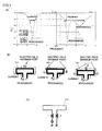
Fig. 1(A) , three resonances (resonance 1,resonance 2 and resonance 3) are used to cover a plurality of frequency bands. In other words,resonance 1 forms a passband in a Low Band whileresonance 2 and resonance 3 form a band in a High Band. - As shown in
Fig. 1 (B) ,resonance 1 is caused by fundamental waves in the odd mode, and shows a resonance mode having monopole-type current distribution in which the intermediate point ofloop antenna 101 is defined as an electric field maximum point.Resonance 2 occurs in the even mode, and shows a resonance mode having dipole-type current distribution in which there are two electric field maximum points onloop antenna 101. Resonance 3 is caused by harmonics in the odd mode, and shows a resonance mode having current distribution as shown in the figure in which there are three electric field maximum points onloop antenna 101. In this case, the "odd mode" represents a mode in the state where the current direction from the power feed end to the radiation element and the current direction from the ground end to the radiation element are aligned with each other. The "even mode" represents a mode in the state where the current direction from the power feed end to the radiation element and the current direction from the ground end to the radiation element are opposite to each other. - The resonance frequency of each resonance can be determined by the size of
loop antenna 101. On the other hand, when this resonance frequency is controlled in a matching circuit, it is conceivable to implement a configuration in which an inductance element L1 and an inductance element L2 are loaded at the power feed end and the ground end, respectively, of the antenna, as shown inFig. 1(C) . - However, when inductance elements are loaded in this way to adjust the frequency, the amount of change in each resonance frequency is increased as the frequency is higher. In other words, by the method of simply loading an inductance element, it is difficult to independently control the resonance frequency for each resonance mode.
- The present invention has been made in light of the above-described circumstances, and an object of the present invention is to provide a multiband-capable antenna device exhibiting excellent frequency characteristics, by which a resonance frequency in each resonance mode can be independently controlled in an antenna element having a plurality of resonance modes, and to provide a communication terminal apparatus using this antenna device.
- Specifically, an antenna device of the present invention relates to an antenna device characterized by including a radiation element configured to include a first conductor having one end as a power feed end and a second conductor having one end as a ground end; and a matching circuit configured to include a first inductance element loaded at the power feed end of the first conductor, and a second inductance element loaded at the ground end of the second conductor and magnetic-field coupled to the first inductance element. The radiation element is configured to resonate in a plurality of resonance modes including an even mode and an odd mode. The first inductance element and the second inductance element are wound and connected such that magnetic fields are mutually strengthened for one of the even mode and the odd mode, and that the magnetic fields are mutually weakened for the other of the even mode and the odd mode.
- Furthermore, a communication terminal apparatus of the present invention relates to a communication terminal apparatus characterized by including a power feed element; a radiation element configured to include a first conductor having one end as a power feed end and a second conductor having one end as a ground end; and a matching circuit configured to include a first inductance element loaded at the power feed end of the first conductor, and a second inductance element loaded at the ground end of the second conductor and magnetic-field coupled to the first inductance element. The radiation element is configured to resonate in a plurality of resonance modes including an even mode and an odd mode. The first inductance element and the second inductance element are wound and connected such that magnetic fields are mutually strengthened for one of the even mode and the odd mode, and that the magnetic fields are mutually weakened for the other of the even mode and the odd mode.
- According to the present invention, since resonance frequencies in a plurality of resonance modes in a radiation element can be controlled independently, a multiband-capable antenna device exhibiting excellent frequency characteristics can be implemented. Furthermore, a multiband-capable communication terminal apparatus exhibiting excellent frequency characteristics can be implemented using this antenna device.
-
-
Fig. 1 illustrates a graph (A) showing frequency characteristics of a loop antenna, a schematic diagram (B) for illustrating the operation principle in each resonance mode, and an equivalent circuit diagram (C) of an antenna device having an inductance element loaded in a loop antenna. -
Fig. 2 is an equivalent circuit diagram of an antenna device according to the first embodiment. -
Fig. 3 is an exploded view of a matching circuit element in the antenna device according to the first embodiment. -
Fig. 4 shows a schematic plan view (A) and a schematic cross-sectional view (B) of a communication terminal apparatus according to the first embodiment. -
Fig. 5 is a schematic diagram for illustrating the operation principle of the antenna device according to the first embodiment. -
Fig. 6 is a graph showing frequency characteristics of the antenna device according to the first embodiment. -
Fig. 7 is an equivalent circuit diagram of an antenna device according to the second embodiment. -
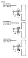
Fig. 8 is a schematic diagram for illustrating the operation principle of the antenna device according the second embodiment. -
Fig. 9 is a graph showing frequency characteristics of the antenna device according to the second embodiment. -
Fig. 10 is an equivalent circuit diagram of an antenna device according to the third embodiment. - An antenna device and a communication terminal apparatus of the present invention will be hereinafter described based on the first to third embodiments.
- The antenna device according to the present embodiment employs 824 to 960 MHz (Low Band) and 1710 to 2170 MHz (High Band) as a passband, and accommodates a penta-band of GSM850, GSM900, GSM1800, GSM1900, and UMTS.
- This antenna device utilizes a loop-
shaped radiation element 11 having an electric length of one wavelength as a radiation element, as shown inFig. 2 . Loop-shaped radiation element 11 has one end (terminal P2) as a power feed end connected to a power feed element, and the other end (terminal P3) as a ground end connected to the ground. This loop-shaped radiation element 11 is shaped such that the first conductor having one end as a power feed end and the second conductor having one end as a ground end are connected at their respective other ends, and can be regarded as a folded dipole antenna. This loop-shaped radiation element 11 has a plurality of resonance modes, which will be described later in detail. - A first inductance element L1 and a second inductance element L2 are loaded at the power feed end and the ground end, respectively, of loop-
shaped radiation element 11. In other words, the first inductance element has one end (terminal P1) to which the power feed element is connected, and the other end (terminal P2) to which one end (the power feed end) of loop-shaped radiation element 11 is connected. The second inductance element has one end (terminal P4) to which the ground is connected, and the other end (terminal P3) to which the other end (the ground end) of loop-shaped radiation element 11 is connected. First inductance element L1 and second inductance element L2 are coupled (additive polarity coupled) through the magnetic field to each other, and form a matching circuit (a matching circuit element 12). - As shown in
Fig. 3 , the matching circuit formed of inductance element L1 and inductance element L2 is configured as a chip component (matching circuit element 12) formed using a stacked body as an element body that is obtained by stacking a plurality of base material layers 13a, 13b, 13c, 13d, and 13e. In other words, each set of inductance element L1 and inductance element L2 is formed integrally with the stacked body formed by stacking base material layers 13a, 13b, 13c, 13d, and 13e. The stacked body has a back surface on which eight terminals are formed, including four terminals P1 to P4 each serving as an input/output terminal connected to a corresponding inductance element, and other four terminals each serving as an NC (non-contact) terminal. - In this stacked body, terminal P1 is connected through a via-
hole conductor 14 provided in base material layer 13a, via-hole conductor 14 provided in base material layer 13b and via-hole conductor 14 provided in base material layer 13c to one end of the conductor pattern having a half-turn coil shape and provided in base material layer 13c. The other end of this conductor pattern is connected through via-hole conductor 14 provided in base material layer 13c to one end of the conductor pattern having a half-turn coil shape and provided in base material layer 13b. The other end of this conductor pattern is connected through via-hole conductor 14 provided in base material layer 13b to one end of the conductor pattern having a half-turn coil shape and provided in base material layer 13a. The other end of this conductor pattern is connected through via-hole conductor 14 provided in base material layer 13a to terminal P2 provided on the back surface of the stacked body. First inductance element L1 is formed by these conductor patterns and via-hole conductors. - Similarly, terminal P4 is connected through via-
hole conductor 14 provided in base material layer 13a, via-hole conductor 14 provided in base material layer 13b, via-hole conductor 14 provided in base material layer 13c, and via-hole conductor 14 provided in base material layer 13d to one end of the conductor pattern having one-turn coil shape and provided in base material layer 13d. The other end of this conductor pattern is connected through via-hole conductor 14 provided in base material layer 13d to one end of the conductor pattern having a half-turn coil shape and provided in base material layer 13c. The other end of this conductor pattern is connected through via-hole conductor 14 provided in base material layer 13c to one end of the conductor pattern having a half-turn coil shape and provided in base material layer 13b. The other end of this conductor pattern is connected through via-hole conductor 14 provided in base material layer 13b to one end of the conductor pattern having a half-turn coil shape and provided in base material layer 13a. The other end of this conductor pattern is connected through via-hole conductor 14 provided in base material layer 13a to terminal P3 provided on the back surface of the stacked body. Second inductance element L2 is formed by these conductor patterns and via-hole conductors 14. - Each of base material layers 13a to 13e may be a ceramic layer like an LTCC ceramic layer, or may be a resin layer like a thermoplastic resin or a thermosetting resin. In other words, the stacked body may be a ceramic stacked body or may be a resin stacked body. An in-plane conductor and an interlayer connection conductor (via-hole conductor) provided in each of base material layers 13a to 13e are formed of a metal material including silver, copper or the like as a main component and having a relatively low specific resistance.
- The communication terminal apparatus according to the present embodiment is a mobile phone accommodating a penta-band of GSM850, GSM900, GSM1800, GSM1900, and UMTS.
- This
communication terminal apparatus 20 includes aterminal housing 21 having a rectangular outer shape, as shown inFig. 4 . Thisterminal housing 21 is equipped with a first printedwiring board 22, abattery pack 23, a second printedwiring board 24, a liquid crystal display element (not shown), and the like. Each of first printedwiring board 22 and second printedwiring board 24 is provided with a ground (not shown) having an area that is approximately equal to those of their main surfaces. On the surface of each ground, various types of functional circuit components such as a drive circuit of a display element, a control circuit of a power supply and anIC chip 25 for cellular communication are mounted. Loop-shapedradiation element 26 is formed by affixing a sheet of a flexible base material having a loop pattern formed thereon onto the inner wall surface near the end ofterminal housing 21. Loop-shapedradiation element 26 has one end connected to matchingcircuit element 28 mounted on first printedwiring board 22 via acontact pin 27 provided on first printedwiring board 22, and also has the other end connected similarly to matchingcircuit element 28 similarly viacontact pin 27 provided on first printedwiring board 22. The power feed-side terminal (terminal P1) of matchingcircuit element 28 is connected toIC chip 25 for cellular communication mounted on first printedwiring board 22 while the ground-side terminal (terminal P4) of matchingcircuit element 28 is connected to the ground of first printedwiring board 22. - Loop-shaped
antenna element 26 according to the present embodiment has three resonance modes including the first resonance mode (resonance 1), the second resonance mode (resonance 2) and the third resonance mode (resonance 3) in increasing order of a resonance frequency. The first resonance mode and the third resonance mode each are an odd mode while the second resonance mode is an even mode. As shown inFigs. 5 and6 ,resonance 1 is caused by fundamental waves in the odd mode, and shows a resonance mode having monopole-type current distribution in which the intermediate point of the loop antenna is defined as an electric field maximum point.Resonance 1 has a resonance frequency in the Low Band.Resonance 2 occurs in the even mode, and shows a resonance mode having dipole-type current distribution in which there are two electric field maximum points on the loop antenna. Thisresonance 2 exhibits resonance on the low-frequency side in the High Band. Resonance 3 is caused by harmonics in the odd mode, and shows a resonance mode having current distribution as shown in the figure, in which there are three electric field maximum points on the loop antenna. This resonance 3 exhibits resonance on the high-frequency side in the High Band. - As described above, the "odd mode" is a mode in the state where the current direction from the power feed end to the radiation element and the current direction from the ground end to the radiation element are aligned with each other, and is a transmission mode where inductance element L1 and inductance element L2 have voltages having different polarities. The "even mode" is a mode in the state where the current direction from the power feed end to the radiation element and the current direction from the ground end to the radiation element are opposite to each other, and is a transmission mode where inductance element L1 and inductance element L2 have voltages having the same polarity.
- In the present embodiment, inductance element L1 and inductance element L2 are wound and connected such that the magnetic fields are mutually strengthened for the odd mode, and that the magnetic fields are mutually weakened for the even mode. Therefore, as shown in
Fig. 5 , forresonance 1 and resonance 3, inductance element L1 and inductance element L2 each act as an inductance element having a large L value since their magnetic fields are mutually strengthened. On the other hand, forresonance 2, the magnetic fields generated in inductance element L1 and inductance element L2 are mutually weakened. More specifically, the magnetic field generated in each inductance element is cancelled. Therefore, according to the configuration of the present embodiment, as shown inFig. 6 , only the resonance frequencies ofresonance 1 and resonance 3 can be selectively shifted to the low-pass side without greatly shifting the resonance frequency of the resonance 2 (more strictly, the frequency of resonance 3 is shifted more than the frequency of resonance 1). - Although the antenna device according to the present embodiment has a configuration basically similar to that of the antenna device according to the first embodiment, first inductance element L1 and second inductance element L2 are coupled (subtractive polarity coupled) through the magnetic field, as shown in
Fig. 7 . Specifically, the power feed end of loop-shapedradiation element 11 is connected to terminal P2 of matchingcircuit element 12, and the ground end of loop-shapedradiation element 11 is connected to terminal P4 of matchingcircuit element 12. In other words, inductance element L1 and inductance element L2 are wound and connected such that the magnetic fields are mutually weakened for the odd mode, and that the magnetic fields are mutually strengthened for the even mode. Therefore, as shown inFig. 8 , forresonance 1 and resonance 3, the magnetic fields are mutually weakened in inductance element L1 and inductance element L2, and the magnetic fields generated in inductance element L1 and inductance element L2 are canceled. On the other hand, forresonance 2, the magnetic fields generated in inductance element L1 and inductance element L2 are mutually strengthened. Therefore, as shown inFig. 9 , only the resonance frequency ofresonance 2 can be selectively shifted to the low-pass side without greatly shifting the resonance frequencies ofresonance 1 and resonance 3. - As shown in
Fig. 10 , in the antenna device according to the present embodiment, the first conductor and the second conductor, which form a radiation element, each have the other end as an open end. The first conductor is configured as a power feed radiation element (a first radiation element 31), and the second conductor is configured as a non-power feed radiation element (a second radiation element 32). The radiation element formed of the first radiation element and the second radiation element resonates in a plurality of resonance modes including an even mode and an odd mode. The first inductance element and the second inductance element forming a matching circuit are wound and connected such that the magnetic fields are mutually strengthened for one of the even mode and the odd mode, and that the magnetic fields are mutually weakened for the other of the even mode and the odd mode. - Although the present invention has been described with reference to specific embodiments, the present invention is not limited to these embodiments.
- For example, the radiation element (antenna element) only has to be configured to include the first conductor having one end as a power feed end and the second conductor having one end as a ground end, and to resonate in a plurality of resonance modes including an even mode and an odd mode. In other words, the shapes of the power feed radiation element and the non-power feed radiation element are not limited to a simple monopole type, but may be various types of shapes such as a folded type and a T-branch type.
- Furthermore, the radiation element is not limited to a pattern formed on a flexible substrate. For example, a chip antenna made of a dielectric element body having an antenna pattern formed thereon may be utilized, or a conductor pattern directly rendered on a printed wiring board or a terminal housing may be utilized.
- Furthermore, the first inductance element and the second inductance element are not limited to a coiled element formed by winding a conductor pattern in a coil shape, but may be a magnetic coupling element which is categorized as a type based on magnetic-field coupling.
- L1: first inductance element, L2: second inductance element, 11: loop-shaped radiation element, 12: matching circuit element, 13a to 13e: base material layer, 14: via-hole conductor, 20: communication terminal apparatus, 21: terminal housing, 22: first printed wiring board, 23: battery pack, 24: second printed wiring board, 25: IC chip for communication, 26: loop-shaped radiation element, 27: contact pin, 28: matching circuit element, 31: first radiation element, 32: second radiation element.
Claims (6)
- An antenna device comprising:a radiation element configured to include a first conductor having one end as a power feed end and a second conductor having one end as a ground end; anda matching circuit configured to include a first inductance element loaded at said power feed end of said first conductor, and a second inductance element loaded at said ground end of said second conductor and magnetic-field coupled to said first inductance element,said radiation element being configured to resonate in a plurality of resonance modes including an even mode and an odd mode, andsaid first inductance element and said second inductance element being wound and connected such that magnetic fields are mutually strengthened for one of said even mode and said odd mode, and that the magnetic fields are mutually weakened for the other of said even mode and said odd mode.
- The antenna device according to claim 1, wherein said radiation element has a first resonance mode, a second resonance mode and a third resonance mode in increasing order of a resonance frequency, said first resonance mode and said third resonance mode each are an odd mode, and said second resonance mode is an even mode.
- The antenna device according to claim 1 or 2, wherein the other end of said first conductor and the other end of said second conductor are connected, and said radiation element forms a loop-shaped radiation element.
- The antenna device according to claim 1 or 2, wherein said first conductor and said second conductor each have the other end as an open end, said first conductor is configured as a power feed radiation element, and said second conductor is configured as a non-power feed radiation element.
- The antenna device according to any one of claims 1 to 4, wherein said first inductance element and said second inductance element are formed integrally with a stacked body formed by stacking a plurality of base material layers.
- A communication terminal apparatus comprising:a power feed element;a radiation element configured to include a first conductor having one end as a power feed end and a second conductor having one end as a ground end; anda matching circuit configured to include a first inductance element loaded at said power feed end of said first conductor, and a second inductance element loaded at said ground end of said second conductor and magnetic-field coupled to said first inductance element,said radiation element being configured to resonate in a plurality of resonance modes including an even mode and an odd mode, andsaid first inductance element and said second inductance element being wound and connected such that magnetic fields are mutually strengthened for one of said even mode and said odd mode, and that the magnetic fields are mutually weakened for the other of said even mode and said odd mode.
Applications Claiming Priority (2)
| Application Number | Priority Date | Filing Date | Title |
|---|---|---|---|
| JP2012187238 | 2012-08-28 | ||
| PCT/JP2013/072673 WO2014034587A1 (en) | 2012-08-28 | 2013-08-26 | Antenna device, and communication terminal device |
Publications (2)
| Publication Number | Publication Date |
|---|---|
| EP2741366A1 true EP2741366A1 (en) | 2014-06-11 |
| EP2741366A4 EP2741366A4 (en) | 2015-02-25 |
Family
ID=50183399
Family Applications (1)
| Application Number | Title | Priority Date | Filing Date |
|---|---|---|---|
| EP13831926.4A Withdrawn EP2741366A4 (en) | 2012-08-28 | 2013-08-26 | Antenna device, and communication terminal device |
Country Status (6)
| Country | Link |
|---|---|
| US (1) | US9153865B2 (en) |
| EP (1) | EP2741366A4 (en) |
| JP (1) | JP5505581B1 (en) |
| CN (1) | CN104025379B (en) |
| DE (2) | DE202013012361U1 (en) |
| WO (1) | WO2014034587A1 (en) |
Families Citing this family (16)
| Publication number | Priority date | Publication date | Assignee | Title |
|---|---|---|---|---|
| JP5994500B2 (en) * | 2012-09-07 | 2016-09-21 | 株式会社村田製作所 | Coupling degree adjusting element, antenna device, and wireless communication device |
| CN207490881U (en) * | 2015-03-11 | 2018-06-12 | 株式会社村田制作所 | Impedance transformation element and communication device |
| KR102330024B1 (en) * | 2015-03-27 | 2021-11-23 | 삼성전자 주식회사 | Antenna apparatus and electronic device including the same |
| CN106025557A (en) * | 2016-06-30 | 2016-10-12 | 厦门恩匹令克科技有限公司 | Class loop antenna of wearable equipment |
| CN112002993B (en) * | 2016-11-29 | 2023-09-19 | 株式会社村田制作所 | Antenna devices and electronic equipment |
| TWM545375U (en) * | 2016-12-27 | 2017-07-11 | 啓碁科技股份有限公司 | Antenna structure |
| WO2019017098A1 (en) * | 2017-07-21 | 2019-01-24 | 株式会社村田製作所 | Antenna coupling element, antenna device, and electronic equipment |
| US11245188B2 (en) * | 2018-01-11 | 2022-02-08 | Mediatek Inc. | Antenna device having a dipole antenna and a loop shaped antenna integrated for improving antenna bandwidth and antenna gain |
| JP6760545B2 (en) * | 2018-04-25 | 2020-09-23 | 株式会社村田製作所 | Antenna coupling element, antenna device and communication terminal device |
| WO2019208044A1 (en) * | 2018-04-25 | 2019-10-31 | 株式会社村田製作所 | Antenna device and communication terminal apparatus |
| WO2019208253A1 (en) * | 2018-04-25 | 2019-10-31 | 株式会社村田製作所 | Antenna device and communication terminal apparatus |
| JP6678721B1 (en) * | 2018-10-31 | 2020-04-08 | 京セラ株式会社 | Antenna, wireless communication module and wireless communication device |
| WO2020137375A1 (en) | 2018-12-28 | 2020-07-02 | 株式会社村田製作所 | Antenna device |
| US20230275349A1 (en) * | 2020-07-27 | 2023-08-31 | Kyocera Corporation | Antenna, wireless communication module, package receiving apparatus, and package receiving system |
| US12224502B2 (en) * | 2021-10-14 | 2025-02-11 | Aptiv Technologies AG | Antenna-to-printed circuit board transition |
| CN118430948B (en) * | 2024-03-05 | 2025-04-11 | 北京平头哥信息技术有限公司 | Reverse coupled inductor and chip |
Family Cites Families (14)
| Publication number | Priority date | Publication date | Assignee | Title |
|---|---|---|---|---|
| US2320124A (en) * | 1941-01-18 | 1943-05-25 | Colonial Radio Corp | Radio receiver for horizontally polarized waves |
| JP3658639B2 (en) * | 2000-04-11 | 2005-06-08 | 株式会社村田製作所 | Surface mount type antenna and radio equipped with the antenna |
| JP4510244B2 (en) | 2000-07-19 | 2010-07-21 | パナソニック株式会社 | Antenna device |
| JP4228559B2 (en) * | 2001-08-08 | 2009-02-25 | 株式会社村田製作所 | Surface mount antenna and communication device using the same |
| SE0402945D0 (en) * | 2004-11-30 | 2004-11-30 | Abb Research Ltd | Industrial robot |
| CN102780085A (en) * | 2006-04-14 | 2012-11-14 | 株式会社村田制作所 | Antenna |
| US8219060B2 (en) * | 2006-07-28 | 2012-07-10 | Qualcomm Incorporated | Dual inductor circuit for multi-band wireless communication device |
| JP2009206975A (en) * | 2008-02-28 | 2009-09-10 | Murata Mfg Co Ltd | Magnetic body antenna, and antenna apparatus |
| JP5316638B2 (en) * | 2009-03-13 | 2013-10-16 | 株式会社村田製作所 | Antenna device |
| EP2388858B1 (en) * | 2010-01-19 | 2016-09-21 | Murata Manufacturing Co., Ltd. | Antenna device and communication terminal apparatus |
| US8325103B2 (en) * | 2010-05-07 | 2012-12-04 | Nokia Corporation | Antenna arrangement |
| WO2012099085A1 (en) * | 2011-01-20 | 2012-07-26 | 株式会社村田製作所 | Frequency stabilizer circuit, antenna device and communication terminal device |
| JP5505561B2 (en) * | 2011-05-09 | 2014-05-28 | 株式会社村田製作所 | Coupling degree adjusting circuit, antenna device, and communication terminal device |
| JP5590060B2 (en) * | 2012-03-28 | 2014-09-17 | 株式会社村田製作所 | Multiband antenna device design method |
-
2013
- 2013-08-26 DE DE202013012361.3U patent/DE202013012361U1/en not_active Expired - Lifetime
- 2013-08-26 CN CN201380003712.2A patent/CN104025379B/en active Active
- 2013-08-26 EP EP13831926.4A patent/EP2741366A4/en not_active Withdrawn
- 2013-08-26 WO PCT/JP2013/072673 patent/WO2014034587A1/en not_active Ceased
- 2013-08-26 DE DE202013012360.5U patent/DE202013012360U1/en not_active Expired - Lifetime
- 2013-08-26 JP JP2013557695A patent/JP5505581B1/en active Active
-
2014
- 2014-04-08 US US14/247,271 patent/US9153865B2/en active Active
Also Published As
| Publication number | Publication date |
|---|---|
| JP5505581B1 (en) | 2014-05-28 |
| DE202013012361U1 (en) | 2016-06-20 |
| CN104025379B (en) | 2016-01-27 |
| US9153865B2 (en) | 2015-10-06 |
| JPWO2014034587A1 (en) | 2016-08-08 |
| EP2741366A4 (en) | 2015-02-25 |
| WO2014034587A1 (en) | 2014-03-06 |
| DE202013012360U1 (en) | 2016-06-21 |
| US20140218246A1 (en) | 2014-08-07 |
| CN104025379A (en) | 2014-09-03 |
Similar Documents
| Publication | Publication Date | Title |
|---|---|---|
| US9153865B2 (en) | Antenna device and communication terminal apparatus | |
| US9997834B1 (en) | Antenna device and communication terminal apparatus | |
| US9692128B2 (en) | Antenna device and wireless communication device | |
| JP6015830B2 (en) | ANTENNA DEVICE AND ELECTRONIC DEVICE | |
| US9865924B2 (en) | Antenna device and communication terminal apparatus | |
| US10936933B2 (en) | Antenna device and electronic device | |
| CN103620868B (en) | Antenna device and communication terminal device | |
| US10664738B2 (en) | Feeder coil, antenna device, and electronic appliance | |
| CN102474005A (en) | Frequency stabilization circuit, frequency stabilization device, antenna device, communication terminal equipment, and impedance transformation element | |
| JP2013168894A (en) | Antenna device and communication terminal having the same | |
| US20170317425A1 (en) | Antenna device and electronic device | |
| US8797225B2 (en) | Antenna device and communication terminal apparatus | |
| US10629988B2 (en) | Antenna device and electronic device | |
| CN207910065U (en) | Antenna devices and electronic equipment | |
| JP5672415B2 (en) | Communication terminal device | |
| CN207149699U (en) | Antenna device and electronic equipment |
Legal Events
| Date | Code | Title | Description |
|---|---|---|---|
| PUAI | Public reference made under article 153(3) epc to a published international application that has entered the european phase |
Free format text: ORIGINAL CODE: 0009012 |
|
| 17P | Request for examination filed |
Effective date: 20140305 |
|
| AK | Designated contracting states |
Kind code of ref document: A1 Designated state(s): AL AT BE BG CH CY CZ DE DK EE ES FI FR GB GR HR HU IE IS IT LI LT LU LV MC MK MT NL NO PL PT RO RS SE SI SK SM TR |
|
| A4 | Supplementary search report drawn up and despatched |
Effective date: 20150128 |
|
| RIC1 | Information provided on ipc code assigned before grant |
Ipc: H01Q 7/00 20060101ALI20150122BHEP Ipc: H01Q 9/30 20060101ALI20150122BHEP Ipc: H01P 5/08 20060101ALI20150122BHEP Ipc: H01Q 1/50 20060101AFI20150122BHEP |
|
| DAX | Request for extension of the european patent (deleted) | ||
| 17Q | First examination report despatched |
Effective date: 20151126 |
|
| STAA | Information on the status of an ep patent application or granted ep patent |
Free format text: STATUS: THE APPLICATION IS DEEMED TO BE WITHDRAWN |
|
| 18D | Application deemed to be withdrawn |
Effective date: 20160607 |