EP2741113A1 - Integrated photonic devices with reduced sensitivity to external influences - Google Patents
Integrated photonic devices with reduced sensitivity to external influences Download PDFInfo
- Publication number
- EP2741113A1 EP2741113A1 EP20130196054 EP13196054A EP2741113A1 EP 2741113 A1 EP2741113 A1 EP 2741113A1 EP 20130196054 EP20130196054 EP 20130196054 EP 13196054 A EP13196054 A EP 13196054A EP 2741113 A1 EP2741113 A1 EP 2741113A1
- Authority
- EP
- European Patent Office
- Prior art keywords
- arm
- wavelength
- wave
- waveguide
- spr
- Prior art date
- Legal status (The legal status is an assumption and is not a legal conclusion. Google has not performed a legal analysis and makes no representation as to the accuracy of the status listed.)
- Granted
Links
Images




Classifications
-
- G—PHYSICS
- G02—OPTICS
- G02F—OPTICAL DEVICES OR ARRANGEMENTS FOR THE CONTROL OF LIGHT BY MODIFICATION OF THE OPTICAL PROPERTIES OF THE MEDIA OF THE ELEMENTS INVOLVED THEREIN; NON-LINEAR OPTICS; FREQUENCY-CHANGING OF LIGHT; OPTICAL LOGIC ELEMENTS; OPTICAL ANALOGUE/DIGITAL CONVERTERS
- G02F1/00—Devices or arrangements for the control of the intensity, colour, phase, polarisation or direction of light arriving from an independent light source, e.g. switching, gating or modulating; Non-linear optics
- G02F1/01—Devices or arrangements for the control of the intensity, colour, phase, polarisation or direction of light arriving from an independent light source, e.g. switching, gating or modulating; Non-linear optics for the control of the intensity, phase, polarisation or colour
- G02F1/011—Devices or arrangements for the control of the intensity, colour, phase, polarisation or direction of light arriving from an independent light source, e.g. switching, gating or modulating; Non-linear optics for the control of the intensity, phase, polarisation or colour in optical waveguides, not otherwise provided for in this subclass
-
- G—PHYSICS
- G02—OPTICS
- G02B—OPTICAL ELEMENTS, SYSTEMS OR APPARATUS
- G02B6/00—Light guides; Structural details of arrangements comprising light guides and other optical elements, e.g. couplings
- G02B6/24—Coupling light guides
- G02B6/26—Optical coupling means
- G02B6/28—Optical coupling means having data bus means, i.e. plural waveguides interconnected and providing an inherently bidirectional system by mixing and splitting signals
- G02B6/293—Optical coupling means having data bus means, i.e. plural waveguides interconnected and providing an inherently bidirectional system by mixing and splitting signals with wavelength selective means
- G02B6/29379—Optical coupling means having data bus means, i.e. plural waveguides interconnected and providing an inherently bidirectional system by mixing and splitting signals with wavelength selective means characterised by the function or use of the complete device
- G02B6/29398—Temperature insensitivity
-
- G—PHYSICS
- G02—OPTICS
- G02B—OPTICAL ELEMENTS, SYSTEMS OR APPARATUS
- G02B6/00—Light guides; Structural details of arrangements comprising light guides and other optical elements, e.g. couplings
- G02B6/10—Light guides; Structural details of arrangements comprising light guides and other optical elements, e.g. couplings of the optical waveguide type
- G02B6/12—Light guides; Structural details of arrangements comprising light guides and other optical elements, e.g. couplings of the optical waveguide type of the integrated circuit kind
- G02B6/12007—Light guides; Structural details of arrangements comprising light guides and other optical elements, e.g. couplings of the optical waveguide type of the integrated circuit kind forming wavelength selective elements, e.g. multiplexer, demultiplexer
-
- G—PHYSICS
- G02—OPTICS
- G02B—OPTICAL ELEMENTS, SYSTEMS OR APPARATUS
- G02B6/00—Light guides; Structural details of arrangements comprising light guides and other optical elements, e.g. couplings
- G02B6/10—Light guides; Structural details of arrangements comprising light guides and other optical elements, e.g. couplings of the optical waveguide type
- G02B6/12—Light guides; Structural details of arrangements comprising light guides and other optical elements, e.g. couplings of the optical waveguide type of the integrated circuit kind
- G02B6/122—Basic optical elements, e.g. light-guiding paths
- G02B6/1225—Basic optical elements, e.g. light-guiding paths comprising photonic band-gap structures or photonic lattices
-
- G—PHYSICS
- G02—OPTICS
- G02B—OPTICAL ELEMENTS, SYSTEMS OR APPARATUS
- G02B6/00—Light guides; Structural details of arrangements comprising light guides and other optical elements, e.g. couplings
- G02B6/10—Light guides; Structural details of arrangements comprising light guides and other optical elements, e.g. couplings of the optical waveguide type
- G02B6/12—Light guides; Structural details of arrangements comprising light guides and other optical elements, e.g. couplings of the optical waveguide type of the integrated circuit kind
- G02B6/122—Basic optical elements, e.g. light-guiding paths
- G02B6/125—Bends, branchings or intersections
-
- G—PHYSICS
- G02—OPTICS
- G02B—OPTICAL ELEMENTS, SYSTEMS OR APPARATUS
- G02B6/00—Light guides; Structural details of arrangements comprising light guides and other optical elements, e.g. couplings
- G02B6/24—Coupling light guides
- G02B6/26—Optical coupling means
- G02B6/28—Optical coupling means having data bus means, i.e. plural waveguides interconnected and providing an inherently bidirectional system by mixing and splitting signals
- G02B6/293—Optical coupling means having data bus means, i.e. plural waveguides interconnected and providing an inherently bidirectional system by mixing and splitting signals with wavelength selective means
- G02B6/29346—Optical coupling means having data bus means, i.e. plural waveguides interconnected and providing an inherently bidirectional system by mixing and splitting signals with wavelength selective means operating by wave or beam interference
- G02B6/29347—Loop interferometers, e.g. Sagnac, loop mirror
-
- G—PHYSICS
- G02—OPTICS
- G02F—OPTICAL DEVICES OR ARRANGEMENTS FOR THE CONTROL OF LIGHT BY MODIFICATION OF THE OPTICAL PROPERTIES OF THE MEDIA OF THE ELEMENTS INVOLVED THEREIN; NON-LINEAR OPTICS; FREQUENCY-CHANGING OF LIGHT; OPTICAL LOGIC ELEMENTS; OPTICAL ANALOGUE/DIGITAL CONVERTERS
- G02F1/00—Devices or arrangements for the control of the intensity, colour, phase, polarisation or direction of light arriving from an independent light source, e.g. switching, gating or modulating; Non-linear optics
- G02F1/01—Devices or arrangements for the control of the intensity, colour, phase, polarisation or direction of light arriving from an independent light source, e.g. switching, gating or modulating; Non-linear optics for the control of the intensity, phase, polarisation or colour
- G02F1/21—Devices or arrangements for the control of the intensity, colour, phase, polarisation or direction of light arriving from an independent light source, e.g. switching, gating or modulating; Non-linear optics for the control of the intensity, phase, polarisation or colour by interference
- G02F1/212—Mach-Zehnder type
-
- G—PHYSICS
- G02—OPTICS
- G02F—OPTICAL DEVICES OR ARRANGEMENTS FOR THE CONTROL OF LIGHT BY MODIFICATION OF THE OPTICAL PROPERTIES OF THE MEDIA OF THE ELEMENTS INVOLVED THEREIN; NON-LINEAR OPTICS; FREQUENCY-CHANGING OF LIGHT; OPTICAL LOGIC ELEMENTS; OPTICAL ANALOGUE/DIGITAL CONVERTERS
- G02F2203/00—Function characteristic
- G02F2203/15—Function characteristic involving resonance effects, e.g. resonantly enhanced interaction
-
- G—PHYSICS
- G02—OPTICS
- G02F—OPTICAL DEVICES OR ARRANGEMENTS FOR THE CONTROL OF LIGHT BY MODIFICATION OF THE OPTICAL PROPERTIES OF THE MEDIA OF THE ELEMENTS INVOLVED THEREIN; NON-LINEAR OPTICS; FREQUENCY-CHANGING OF LIGHT; OPTICAL LOGIC ELEMENTS; OPTICAL ANALOGUE/DIGITAL CONVERTERS
- G02F2203/00—Function characteristic
- G02F2203/21—Thermal instability, i.e. DC drift, of an optical modulator; Arrangements or methods for the reduction thereof
-
- G—PHYSICS
- G02—OPTICS
- G02F—OPTICAL DEVICES OR ARRANGEMENTS FOR THE CONTROL OF LIGHT BY MODIFICATION OF THE OPTICAL PROPERTIES OF THE MEDIA OF THE ELEMENTS INVOLVED THEREIN; NON-LINEAR OPTICS; FREQUENCY-CHANGING OF LIGHT; OPTICAL LOGIC ELEMENTS; OPTICAL ANALOGUE/DIGITAL CONVERTERS
- G02F2203/00—Function characteristic
- G02F2203/60—Temperature independent
Definitions
- the present invention relates to methods for reducing the sensitivity of on-chip integrated photonic devices having a wavelength-dependent transmission or filter characteristic to influences or effects acting on the chip as a whole or on the local environment of the photonic device.
- the invention also relates to on-chip integrated photonic devices having a wavelength-dependent transmission or filter characteristic with a reduced sensitivity to the aforementioned effects.
- thermo-optic coefficient 1 .86 x 10 -4 K -1 . It is a challenge to reduce the temperature sensitivity of such photonic devices, in particular photonic devices with a wavelength-dependent transmission or filter characteristic, especially in combination with a low propagation loss and small footprint.
- the temperature dependence of integrated silicon photonic devices can be reduced by providing an overlay as a top cladding layer, wherein the overlay material (e.g. a polymer) has a thermo-optic coefficient opposite to the thermo-optic coefficient of silicon.
- the overlay material e.g. a polymer
- the use of such an overlay may lead to aging problems and thermal hysteresis.
- a polymer overlay cannot withstand high-temperature treatments typically used in back-end metallization in CMOS processes. Therefore the use of such a polymer overlay is not CMOS compatible.
- MZI Mach-Zehnder interferometer
- integrated silicon photonic devices are very sensitive to variations in line-width and thickness (e.g. induced by the fabrication process) and to ionizing radiation.
- the present invention provides an integrated photonic device having a wavelength-dependent characteristic, the device comprising: a Splitter Polarization Rotator SPR having an input port for receiving polarized light, and a first output port for providing a first wave, and a second output port for providing a second wave; a first arm having dimensions for (mainly) propagating a first polarization mode of the first wave, an input side of the first arm being optically connected to the first output port of the SPR; a second arm having dimensions for(mainly) propagating a second polarization mode of the second wave, the second polarization mode being different from the first polarization mode, an input side of the second arm being optically connected to the second output port of the SPR; and a Polarization Rotator and Combiner PRC having a first input port optically connected to an output side of the first arm for receiving the propagated first wave, and a second input port optically connected to an output side of the second arm for receiving the propagated second wave, and an output port for providing the combination of the propag
- the first arm may be a first waveguide arm.
- the second arm may be a second waveguide arm.
- the dimensions (design parameters) of the first arm and of the second arm can for example include the line-width of the arms, the height of the arms and/or the length of the arms.
- the line-width can be constant along the length of an arm or it can vary along the length of an arm.
- the dimensions of the arms are chosen so as to reduce, e.g. minimize, e.g. substantially cancel out the influence of effects such as temperature variations, geometric tolerances or radiation on an optical characteristic of the photonic device, such as e.g. its transmission characteristic or its filter characteristic.
- Such devices having substantially reduced sensitivity to external effects are further referred to as "compensated devices”.
- fabrication of the photonic devices is compatible with standard processing techniques for integrated photonic devices, e.g. silicon based integrated photonic devices. It is an advantage that there is no need for modifying or adapting fabrication processes.
- the main difference is that in embodiments of the present invention light of two different polarities (e.g. TE and TM) is used, as opposed to only a single polarity (TE) in the prior art.
- the main advantage hereof is that the photonic devices of the present invention can have a small footprint and low losses due to the use of TM polarization.
- the main disadvantage of using only a single polarity is that either the device size is large or the use of very narrow (and therefore lossy) waveguides is required to have a sufficient difference in thermo-optic response between both waveguide arms.
- thermo-optic coefficient opposite to the thermo-optic coefficient of the core material can be avoided.
- problems related to such overlays such as aging and thermal hysteresis, can be avoided.
- the first polarization mode is a Transverse Magnetic mode (TM) and the second polarization mode is a Transverse Electric Mode (TE), or vice versa.
- TM Transverse Magnetic mode
- TE Transverse Electric Mode
- the dimensions of the first arm and the dimensions of the second arm are selected to substantially cancel the influence of at least one effect selected from the group of dimension tolerances, radiation and temperature variations on an optical characteristic of the photonic device.
- the optical characteristic is selected from a transmitted wavelength or a filtered wavelength.
- the dimensions of the first arm and the dimensions of the second arm are adapted to substantially cancel out the influence of temperature variations on said optical characteristic.
- the dimensions of the first and second arm may e.g. be chosen to substantially cancel the influence of temperature variations on a transmitted wavelength characteristic.
- the dimensions of the first and second arm may e.g. be chosen to substantially cancel the influence of temperature variations on a filtered wavelength characteristic.
- the difference in confinement between the first polarization mode in the first arm and the second polarization mode in the second arm induces a different thermo-optic coefficient, thus allowing the influence of temperature on the device characteristics to be cancelled out and thus substantially reducing temperature sensitivity.
- the dimensions of the first arm and the dimensions of the second arm are selected to substantially cancel out the influence of geometrical variations, such as for example variations in line-width, on said optical characteristic.
- the dimensions of the first and second arm may e.g. be chosen to substantially cancel the influence of line-width on a transmitted wavelength characteristic.
- the dimensions of the first and second arm may e.g. be chosen to substantially cancel the influence of line-width on a filtered wavelength characteristic.
- the dimensions of the first arm and the dimensions of the second arm are selected to substantially cancel out the influence of radiation effects, e.g. ionization radiation effects.
- the dimensions of the first and second arm may e.g. be chosen to substantially cancel the influence of radiation-effects on a transmitted wavelength characteristic.
- the dimensions of the first and second arm may e.g. be chosen to substantially cancel the influence of radiation-effects on a filtered wavelength characteristic.
- the device is a wavelength filter, preferably selected from the group of a Mach-Zehnder interferometer (MZI), a ring resonator and an arrayed-waveguide grating.
- MZI Mach-Zehnder interferometer
- the integrated photonic device further comprises:- a wavelength selective modulator, optically coupled to the first arm by a second SPR adapted for coupling light of the first polarization mode from the first arm to light of the second polarization mode in the wavelength selective modulator; and wherein the dimensions of the first arm and dimensions of the second arm are selected to substantially cancel wavelength drift of the wavelength selective modulator due to external effects.
- the wavelength selective modulator may be a ring modulator.
- the invention relates to a method for reducing the sensitivity of an integrated photonic device having a wavelength-dependent characteristic, comprising the steps of:- splitting a light beam in a first wave having a first polarization mode and a second wave having a second polarization mode different from the first polarization mode;- propagating the first wave through a first arm;- propagating the second wave through a second arm;- combining the propagated first wave and the propagated second wave at an output side of the first arm and of the second arm; wherein the dimensions of the first arm and the dimensions of the second arm are selected to substantially cancel out the influence of an external effect on the wavelength-dependent characteristic.
- the first arm may be a first waveguide arm
- the second arm may be a second waveguide arm.
- the external effect may be any effect selected from the group consisting of temperature variations, geometric variations and radiation effects.
- the integrated photonic device is a wavelength filter, preferably selected from the group of a Mach-Zehnder interferometer (MZI), a ring resonator and an arrayed-waveguide grating, and the optical characteristic is a transmission or filter characteristic of said wavelength filter.
- MZI Mach-Zehnder interferometer
- the optical characteristic is a transmission or filter characteristic of said wavelength filter.
- the integrated photonic device further comprises a wavelength selective modulator optically coupled to the first arm; wherein the method further comprises the step of:- coupling light of the first polarization mode from the first arm to light of the second polarization mode in the wavelength selective modulator; and wherein the optical characteristic is a resonance wavelength of the wavelength selective modulator.
- first, second, third and the like in the description are used for distinguishing between similar elements and not necessarily for describing a sequence, either temporally, spatially, in ranking or in any other manner. It is to be understood that the terms so used are interchangeable under appropriate circumstances and that the embodiments of the invention described herein are capable of operation in other sequences than described or illustrated herein.
- top, bottom, over, under and the like in the description are used for descriptive purposes and not necessarily for describing relative positions. It is to be understood that the terms so used are interchangeable under appropriate circumstances and that the embodiments of the invention described herein are capable of operation in other orientations than described or illustrated herein.
- a 'wavelength-selective device' is a photonic device having an intentional, e.g. a predefined, wavelength dependent characteristic, such as a wavelength dependent transmission characteristic or a wavelength-dependent filter characteristic.
- wavelength-selective devices are filters, resonators and ring modulators, the present invention not being limited thereto.
- an 'external effect' can be any effect that acts on the chip as a whole or on the local environment of the photonic device on the chip, such as for example temperature influences, radiation effects or geometrical effects.
- examples are given for embodiments wherein the 'external effect' refers to the temperature.
- the present invention is not limited thereto.
- This invention relates to wavelength-selective on-chip integrated photonic devices having a substantially reduced sensitivity to external effects (further also referred to as 'compensated' devices).
- the present invention relates to wavelength-selective integrated photonic devices having a substantially reduced temperature sensitivity, wherein the need for providing local heaters is avoided, wherein the photonic devices have low propagation losses and a reduced footprint as compared to existing photonic devices, (e.g. as described in US 2011/0102804 ) and wherein the photonic device processing is compatible with standard processing techniques, e.g. compatible with CMOS processing, such that there is no need to modify the manufacturing process.
- silicon photonic waveguide devices are very sensitive to variations in width and height of its structure or elements thereof. It has also been shown that silicon photonic waveguides are sensitive to exposure to ionizing radiation.
- wavelength selective devices in accordance with the present invention can be realised in any suitable material system known by a person skilled in the art.
- Compensated wavelength-selective devices contain two or more delay lines (integrated waveguides, waveguide arms) wherein, in operation, two delay lines propagate a different polarization of light.
- a first delay line or first integrated waveguide propagates (mainly) TM polarized light while a second delay line or second integrated waveguide propagates (mainly) TE polarized light.
- the difference in optical confinement in the waveguide core between both polarizations induces a different response of the waveguide mode to temperature variations. Based on this difference, the effect of temperature on the device characteristics can be reduced, or made to substantially cancel out (compensate), if appropriate design parameters are selected.
- the design parameters can for example include the line-width of the delay lines (wherein the line-width can be constant along the length of a delay line or wherein the line-width can vary along the length of a delay line), the height of the delay lines and/or the length of the delay lines.
- these design parameters cannot be selected independently in order to achieve the reduction or substantial cancellation.
- a waveguide for propagation of TE polarization and a waveguide for propagation of TM polarization are used.
- the TM light is much less confined in a waveguide than the fundamental TE mode, and it experiences a weaker temperature response.
- the propagation loss for the TM mode is lower than for the TE mode, as the TM mode does not have high field intensities on the rough sidewalls of the waveguide core material.
- the device 100 comprises an input waveguide 10 optically connected to an input port of a Splitter Polarization Rotator (SPR) 11.
- SPR Splitter Polarization Rotator
- the SPR 11 is optically connected to an input side of a first waveguide arm 12 (upper waveguide, upper arm in this drawing) and to an input side of a second waveguide arm 13 (lower waveguide, lower arm in this drawing).
- the width of the first waveguide arm 12 and the width the second waveguide arm 13 can be the same or it can be different. It can be selected to obtain a good balance between low propagation loss and a large difference in thermo-optic response.
- the width of both waveguides can be varied. However, in the example further described it is assumed that the width of the waveguides is substantially the same over the entire length of the waveguide arms.
- the width can for example be in the range between about 250 nm and about 1000 nm, e.g. in the order of about 450 nm.
- the MZI device can for example be fabricated in an SOI material system, wherein silicon is used as a core material for the waveguides and wherein a silicon oxide lower cladding layer is used.
- the upper cladding layer can for example be air or a dielectric layer such as an oxide layer or a nitride layer.
- the first waveguide arm 12 and the second waveguide arm 13 are at their output side optically connected to a first resp. second input port of a Polarization Rotator and Combiner (PRC) 14, an output side of the PRC 14 being optically connected to an output waveguide 15.
- PRC Polarization Rotator and Combiner
- the PRC 14 can be a device similar to the SPR 11, but reversed in operation.
- polarized light 1 of a first polarisation state is provided as an input to the SPR 11, for example from an on-chip input waveguide 10 as illustrated in FIG. 1 .
- the polarized light 1 of the first polarisation state passes through the Splitter and Polarization Rotator (SPR) 11 that splits it and converts it into a first wave 2 of a second polarisation state, and a second wave 3 of the first polarisation state.
- SPR Splitter and Polarization Rotator
- TE transverse electric
- polarized light 1 may be provided as an input to the SPR 11, for example from an on-chip input waveguide 10 as illustrated in FIG. 1 .
- the TE polarized light 1 passes through the Splitter and Polarization Rotator (SPR) 11 that splits it and converts it into a first portion, e.g. 50%, transverse magnetic (TM) wave 2 and a second portion, e.g. 50%, transverse electric (TE) wave 3.
- SPR Splitter and Polarization Rotator
- the present invention is not limited to the polarized light 1 being TE polarized. It can also be TM polarized light, that is split into a TM wave and a TE wave by the SPR 11.
- the present invention is not limited to 50%/50% splitting.
- the SPR 11 (and the PRC 14) can be modified to have a different ratio of optical power between the two arms 12, 13, which can for example be used to adjust the balance of the arms to desired specifications, e.g.
- the polarised light 2 of the second polarisation state e.g. TM polarized light 2
- the polarised light 3 of the first polarisation state e.g. TE polarized light 3
- PRC Polarization Rotator and Combiner
- both light waves 2, 3 are coupled to the Polarization Rotator and Combiner (PRC) 14, resulting in a polarised output wave 4 of the first polarisation state, e.g. a TE polarized output wave 4, e.g. propagating in an output waveguide 15 connected to an output port of the Polarization Rotator and Combiner (PRC) 14.
- the output wave 4 results from interference of waves 2 and 3 in both arms, which exhibit a wavelength-dependent response.
- FIG. 2 schematically shows an example of a Splitter and Polarization Rotator (SPR) 11 that can be used in embodiments of photonic devices according to the present invention.
- the lower cladding layer 21 is for example a silicon oxide layer and the upper cladding layer 22 is air.
- FIG. 2(a) shows a cross section of the SPR and FIG. 2(b) shows a top view of the SPR.
- the SPR comprises a first SPR waveguide 111 and a second SPR waveguide 112, the first SPR waveguide 111 and the second SPR waveguide 112 being provided on the lower cladding layer 21 with a small, constant gap g in between the first SPR waveguide 111 and the second SPR waveguide 112 over a predetermined distance or coupling length Lc.
- the gap g is sufficiently small to allow transfer of optical power between the second SPR waveguide 112 and the first SPR waveguide 111.
- the gap size can be in the range between about 50 nm and about 500 nm.
- the width W TE of the second SPR waveguide 112 is different from (in this example: smaller than) the width W TM of the first SPR waveguide 111, to allow mode matching.
- An incoming light wave such as for example a TE wave (e.g. light wave 1 in FIG. 1 ) propagating through second SPR waveguide 112 can couple into first SPR waveguide 111.
- the coupling length Lc is selected to allow about 50% power transfer from the second SPR waveguide 112 (TE mode) to the first SPR waveguide 111 (TM mode).
- a geometric variation e.g. a tapering section
- the output end of the second SPR waveguide 112 (second output port of the SPR 11) is optically connected to second waveguide arm 13 and the output end of the first SPR waveguide 111 (first output port of the SPR 11) is optically connected to first waveguide arm 12.
- Adiabatic tapers or non-adiabatic mode-matching structures can be provided to connect narrower and wider sections of waveguides.
- a Polarization Rotator and Combiner (PRC) 14 as can be used in embodiments of the present invention can have a device structure similar to a Splitter and Polarization Rotator device structure, an example being shown in FIG. 2 , but operated in the reverse direction.
- the PRC 14 comprises a first PRC waveguide and a second PRC waveguide, the first PRC waveguide and the second PRC waveguide being provided on the lower cladding layer 21 with a small, constant gap g' in between the first PRC waveguide and the second PRC waveguide over a predetermined distance or coupling length Lc'.
- the gap g' is sufficiently small to allow transfer of optical power between the first PRC waveguide and the second PRC waveguide.
- the gap size g' can be in the range between about 50 nm and about 500 nm.
- the width of the second PRC waveguide is different from the width of the first PRC waveguide, to allow mode matching.
- a first incoming light wave e.g. light wave 2 in FIG. 1
- a second incoming light wave e.g. light wave 3 in FIG. 1
- the coupling length Lc' between both PRC waveguides is selected to allow full power transfer from the first PRC waveguide (TM mode) to the second PRC waveguide (TE mode).
- the output end of the PRC 14 is optically connected to output waveguide 15.
- Adiabatic tapers or non-adiabatic mode-matching structures can be provided to connect narrower and wider sections of waveguides.
- FIG. 3 shows a schematic cross section of a silicon waveguide with air upper cladding that was used in the simulations.
- the silicon core 20 of the waveguide has a height h and a width w.
- the lower cladding layer 21 is silica and the upper cladding layer 22 is air.
- the height h of the Si waveguide was maintained at 220 nm and the width w was varied.
- the lower cladding layer 21 and the upper cladding layer 22 are assumed to have a thickness of 2 micrometer.
- the dispersion behaviour of the waveguide is shown in FIG. 4 for TE polarized and for TM polarized light (wherein TE00 represents the fundamental TE mode, TM00 represents the fundamental TM mode, TE10 and TE20 represent other modes of the polarized light).
- m ⁇ ⁇ n eff ⁇ ⁇ ⁇ L with m an integer, ⁇ the wavelength of the light, n eff the effective refractive index of the waveguide mode and ⁇ L the path length difference between the first waveguide arm 12 and the second waveguide arm 13.
- m should be a so called "half integer", meaning a value equal to an integer plus 1/2, for example 0.5 ; 1.5 ; 2.5 etc.
- M m - d ⁇ n eff , TM d ⁇ . L 1 - d ⁇ n eff , TE d ⁇ . L 2 M is the modified interference order due to the induced dispersion (influence of wavelength on effective refractive index) related to the difference in effective refractive indices in the different arms.
- the refractive index n of silicon is assumed to be 3.48 and a silicon thermo-optic coefficient of 1.86 ⁇ 10 -4 K -1 is used.
- a refractive index of 1.45 is used and a thermo-optic coefficient of 1 ⁇ 10 -5 K -1 .
- the waveguide width used for both the first waveguide arm 12 and the second waveguide arm 13 of the exemplary interferometer was 450 nm.
- Adiabatic tapers provided between the SPR 11 and the waveguide arms 12, 13 and between the waveguide arms 12, 13 and the PRC 14 are included in the device simulations.
- the n eff is about 2.28 for TE polarized light and about 1.55 for TM polarized light.
- Their calculated thermo-optic coefficients are 2.19 ⁇ 10 -4 K -1 and 9.61 ⁇ 10 -5 K -1 , respectively.
- FIG. 2 schematically illustrates the structure of the SPR 11 in which an input TE signal is split into a TE signal and a TM signal in the wider section due to the phase matching condition and asymmetric structure.
- the gap g between the two SPR waveguides 12, 13 was kept constant as 200 nm over a distance or coupling length Lc.
- the corresponding modified interference plot M is shown in FIG. 7 .
- the asymptotic behaviour of d ⁇ /dT with length L1 ( FIG. 6 ) can be attributed to the zero crossing of M as shown in FIG. 7 .
- the path length difference L1-L2 for temperature insensitive operation is around 25.6 micrometer for this example (the calculated L1 is 45.6 micrometer for the given length L2 of 20 micrometer).
- FIG. 8 shows calculated transmission spectra for a conventional uncompensated MZI with a TM signal in both waveguide arms, for three different temperatures (0oC, 50oC and 100oC).
- FIG. 9 shows calculated transmission spectra for a compensated (temperature insensitive) design with a TM signal in one waveguide arm, and a TE signal in the other waveguide arm, according to embodiments of the present invention, for three different temperatures (0oC, 50oC and 100oC).
- the width of the first (upper) waveguide arm 12 and of the second (lower) waveguide arm 13 of the MZI 100 was 450 nm for all cases and an upper air cladding was assumed.
- the simulated results show an improvement from 80 pm/K drift for an uncompensated MZI ( FIG. 8 ) to less than 0.2 pm/K for a compensated MZI in accordance with the present invention ( FIG. 9 ).
- FIG. 10 shows the thermo-optic coefficient variation (dn eff /dT) as a function of waveguide width for the fundamental TE mode
- FIG. 11 shows the thermo-optic coefficient variation (dn eff /dT) as a function of waveguide width for the fundamental TM mode.
- An about one order of magnitude difference between both can be seen from FIG. 10 and FIG. 11 .
- the SPR 11 (as well as the PRC 14) requires a vertical symmetry breaking to enable mode splitting and polarization conversion. With an air upper cladding 22 and a silica lower cladding 21 (as illustrated in FIG. 2 ) this vertical symmetry breaking is automatically accomplished. In other embodiments, e.g. with a silicon oxide lower cladding and a silicon oxide upper cladding (i.e. wherein the waveguides are fully embedded in silicon oxide) vertical symmetry breaking can be obtained by partially etching one of the two waveguides.
- FIG. 12 schematically illustrates an SPR design (cross section) for embodiments wherein both the lower cladding layer 31 and the upper cladding layer 32 are made of the same material, e.g. silicon oxide.
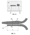
- the SPR waveguides 33, 34 have a different height and width.
- This coupler design operates however in a narrow wavelength band, e.g. having a bandwidth of less than 3.0 nm.
- Wide band operation of an SPR as shown in FIG. 12 can be obtained by varying the width of an SPR waveguide along its length, thus inducing a variation in effective refractive index along the length. This can for example be done by tapering the waveguide from one side and keeping the gap g between the first SPR waveguide 34 and the second SPR waveguide 33 constant.
- FIG. 13 shows an example (top view) of the waveguides of an SPR having a cross section as in FIG. 12 wherein the wider waveguide 33 (propagating the TE mode in this example) is tapered at one lateral side.
- the gap g between the first SPR waveguide 34 and the second SPR waveguide 33 is substantially constant along the coupling length Lc.
- the second SPR waveguide 33 can taper from 680 nm width at one end to 720 nm width at an opposite end. This is advantageous since the thin waveguide section 33 is much more sensitive to width variations, which is undesirable.
- FIG. 14 illustrates power coupling at a wavelength of 1550 nm from the TE mode to the TM mode as a function of coupling length for the coupler design shown FIG. 13 .
- FIG. 15 illustrates power coupling from the TE mode to the TM mode as a function of wavelength for the coupler design of FIG. 13 , showing substantially maximum power transfer from 1540 nm to 1560 nm, which is a substantially broader range than for a design with a constant width for both SPR waveguides.
- the present invention also relates to a so-called “system”, which is in fact also an integrated photonic device 400, but which acts like a “compensated ring modulator”.
- This "compensated ring modulator” in accordance with embodiments of the present invention contains an MZI, and a ring structure 50 optically connected to the first waveguide arm 42 of the MZI, the first waveguide arm being adapted for carrying the TM polarization mode.
- the system 400 functions as a ring modulator operating in the TE polarization mode.
- the system 400 further comprises an SPR (not shown) to couple light from the TM mode propagating in the first waveguide arm 42 to the TE mode in the ring 50.
- the ring structure 50 preferably has a racetrack shape.
- an MZI (comprising the elements 40, 41, 42, 43, 44) is used to passively compensate for temperature-induced wavelength drift of the ring 50.
- An exemplary embodiment is illustrated in FIG. 16 .
- Input light 1 e.g. coming from a grating coupler is split into 50% TE mode and 50% TM mode by the SPR 41. As mentioned above, the ratio does not need to be exactly 50/50.
- the TE beam 3 (mainly) propagates through the second waveguide arm 43 of the MZI and the TM beam 2 (mainly) propagates through the first waveguide arm 42 of the MZI.
- the first waveguide arm 42 is optically coupled with a racetrack p-n junction depletion based ring 50.
- the coupler section of the ring 50 is defined by a shallow etch, with silicon remaining around the core of the waveguide.
- the section is preferably made sufficiently long to overcouple with the ring (i.e. more light is coupled to the ring 50 than needed for critical coupling).
- the cross coupling coefficient kappa 0.4.
- This structure ensures again a TM to TE conversion, hence light 4 coupled into the ring 50 is TE mode light.
- the ring 50 can be modulated in and out of resonance by electrically driving the embedded p-n junction. This modulation is a local effect in the ring 50, and it is not compensated by the temperature insensitive MZI (as described further).
- the signal modulated on the ring 50 is translated into an amplitude and phase response of the light 2 in arm 42.
- L 1 is the length of the first (e.g. upper) arm 42 of the MZI and n 1 is its effective index
- L 2 is the length of the second (e.g. lower) arm 43 of the MZI with effective index n 2
- R is the radius of the ring 50
- n eff is the effective refractive index of the ring 50.
- This approach allows realizing resonator rings 50 and ring modulators 400 with a resonance dip at a predetermined wavelength that is substantially independent of temperature variations. Thermal compensation of the ring 50 is obtained by the balanced MZI.
- TM delay line For each TE arm (TE delay line) a TM arm (TM delay line) is provided, both being connected via an SPR and a PRC, the arms having dimensions (such as e.g. length, width, height) chosen to compensate thermal effects of the TE arm by making the local MZI balanced.
- the method of the present invention can be used to minimize sensitivity to fabrication errors, e.g. fabrication tolerances like width and height variations.
- the method can also be used to minimize sensitivity to other effects such as ionizing radiation.
- the dependence of the effective index of the TE and TM modes on the envisaged effect e.g. line width or radiation
- the equations e.g. equation (4)
Landscapes
- Physics & Mathematics (AREA)
- General Physics & Mathematics (AREA)
- Optics & Photonics (AREA)
- Engineering & Computer Science (AREA)
- Microelectronics & Electronic Packaging (AREA)
- Nonlinear Science (AREA)
- Optical Integrated Circuits (AREA)
- Optical Modulation, Optical Deflection, Nonlinear Optics, Optical Demodulation, Optical Logic Elements (AREA)
Abstract
Description
- The present invention relates to methods for reducing the sensitivity of on-chip integrated photonic devices having a wavelength-dependent transmission or filter characteristic to influences or effects acting on the chip as a whole or on the local environment of the photonic device. The invention also relates to on-chip integrated photonic devices having a wavelength-dependent transmission or filter characteristic with a reduced sensitivity to the aforementioned effects.
- The sensitivity of on-chip integrated photonic devices to external effects acting on the chip or on the local environment of the photonic device is a major issue, in particular for integrated photonic devices with an intentional wavelength-dependent transmission or filter characteristic. The dependence of device characteristics on temperature, geometrical variations (e.g. related to manufacturing tolerances) and/or ionizing radiation, is undesirable for such integrated photonic devices.
- For example, the problem of temperature sensitivity is in particular pronounced for photonic devices made in a material having a high dependence of refractive index on temperature (i.e. a high thermo-optic coefficient). Therefore, temperature dependence is one of the fundamental limitations of silicon photonic devices, because of the high thermo-optic coefficient of silicon (1.86 x 10⁻⁴ K-1). It is a challenge to reduce the temperature sensitivity of such photonic devices, in particular photonic devices with a wavelength-dependent transmission or filter characteristic, especially in combination with a low propagation loss and small footprint.
- The temperature dependence of integrated silicon photonic devices can be reduced by providing an overlay as a top cladding layer, wherein the overlay material (e.g. a polymer) has a thermo-optic coefficient opposite to the thermo-optic coefficient of silicon. However, the use of such an overlay may lead to aging problems and thermal hysteresis. Moreover, a polymer overlay cannot withstand high-temperature treatments typically used in back-end metallization in CMOS processes. Therefore the use of such a polymer overlay is not CMOS compatible.
- Another solution is the use of local heaters to dynamically stabilize the photonic device. However, this requires active temperature monitoring which is space consuming and leads to high power consumption.
- In
US 2011/0102804 a Mach-Zehnder interferometer (MZI) is described that can be made athermal (temperature independent) by using different waveguide arm widths and selecting proper arm lengths such that the temperature sensitivity of one arm cancels that of the other arm. This is based on the different response of the waveguides to changes in temperature because the fraction of light that is confined in the silicon waveguide core is different for both waveguides. - Similarly, integrated silicon photonic devices are very sensitive to variations in line-width and thickness (e.g. induced by the fabrication process) and to ionizing radiation.
- It is an object of embodiments of the present invention to provide a good photonic method and a good photonic device, with a reduced sensitivity to external effects.
- This objective is accomplished by a method and a device according to embodiments of the present invention.
- According to a first aspect, the present invention provides an integrated photonic device having a wavelength-dependent characteristic, the device comprising: a Splitter Polarization Rotator SPR having an input port for receiving polarized light, and a first output port for providing a first wave, and a second output port for providing a second wave; a first arm having dimensions for (mainly) propagating a first polarization mode of the first wave, an input side of the first arm being optically connected to the first output port of the SPR; a second arm having dimensions for(mainly) propagating a second polarization mode of the second wave, the second polarization mode being different from the first polarization mode, an input side of the second arm being optically connected to the second output port of the SPR; and a Polarization Rotator and Combiner PRC having a first input port optically connected to an output side of the first arm for receiving the propagated first wave, and a second input port optically connected to an output side of the second arm for receiving the propagated second wave, and an output port for providing the combination of the propagated first wave and the propagated second wave as an output wave; wherein the dimensions of the first arm and the dimensions of the second arm are selected to substantially cancel out the influence of an external effect on the wavelength-dependent characteristic.
- The first arm may be a first waveguide arm. The second arm may be a second waveguide arm. The dimensions (design parameters) of the first arm and of the second arm can for example include the line-width of the arms, the height of the arms and/or the length of the arms. The line-width can be constant along the length of an arm or it can vary along the length of an arm.
- It is an advantage of embodiments of the present invention that the dimensions of the arms are chosen so as to reduce, e.g. minimize, e.g. substantially cancel out the influence of effects such as temperature variations, geometric tolerances or radiation on an optical characteristic of the photonic device, such as e.g. its transmission characteristic or its filter characteristic. Such devices having substantially reduced sensitivity to external effects are further referred to as "compensated devices".
- It is an advantage of embodiments of the present invention that fabrication of the photonic devices is compatible with standard processing techniques for integrated photonic devices, e.g. silicon based integrated photonic devices. It is an advantage that there is no need for modifying or adapting fabrication processes.
- When compared to the solution proposed in
US2011/0102804 , the main difference is that in embodiments of the present invention light of two different polarities (e.g. TE and TM) is used, as opposed to only a single polarity (TE) in the prior art. The main advantage hereof is that the photonic devices of the present invention can have a small footprint and low losses due to the use of TM polarization. The main disadvantage of using only a single polarity is that either the device size is large or the use of very narrow (and therefore lossy) waveguides is required to have a sufficient difference in thermo-optic response between both waveguide arms. - It is an advantage of embodiments of the present invention that the need for providing an overlay, e.g. a polymer overlay, with a thermo-optic coefficient opposite to the thermo-optic coefficient of the core material, as a top cladding can be avoided. Hence also problems related to such overlays, such as aging and thermal hysteresis, can be avoided.
- It is an advantage of embodiments of the present invention that the need for providing local heaters to dynamically stabilize the photonic devices can be avoided. Therefore high power consumption can be avoided.
- In embodiments of the present invention, the first polarization mode is a Transverse Magnetic mode (TM) and the second polarization mode is a Transverse Electric Mode (TE), or vice versa.
- In embodiments of the present invention, the dimensions of the first arm and the dimensions of the second arm are selected to substantially cancel the influence of at least one effect selected from the group of dimension tolerances, radiation and temperature variations on an optical characteristic of the photonic device.
- In embodiments of the present invention, the optical characteristic is selected from a transmitted wavelength or a filtered wavelength.
- In embodiments of the present invention, the dimensions of the first arm and the dimensions of the second arm are adapted to substantially cancel out the influence of temperature variations on said optical characteristic.
- The dimensions of the first and second arm may e.g. be chosen to substantially cancel the influence of temperature variations on a transmitted wavelength characteristic. Alternatively, the dimensions of the first and second arm may e.g. be chosen to substantially cancel the influence of temperature variations on a filtered wavelength characteristic.
- The difference in confinement between the first polarization mode in the first arm and the second polarization mode in the second arm induces a different thermo-optic coefficient, thus allowing the influence of temperature on the device characteristics to be cancelled out and thus substantially reducing temperature sensitivity.
- In contrast to
US2011/0102804 , where a single polarity was used, the use of different polarizations amplifies the difference in temperature response in both arms without introducing high propagation losses. - In embodiments of the present invention, the dimensions of the first arm and the dimensions of the second arm are selected to substantially cancel out the influence of geometrical variations, such as for example variations in line-width, on said optical characteristic.
- The dimensions of the first and second arm may e.g. be chosen to substantially cancel the influence of line-width on a transmitted wavelength characteristic. Alternatively, the dimensions of the first and second arm may e.g. be chosen to substantially cancel the influence of line-width on a filtered wavelength characteristic.
- In embodiments of the present invention, the dimensions of the first arm and the dimensions of the second arm are selected to substantially cancel out the influence of radiation effects, e.g. ionization radiation effects.
- The dimensions of the first and second arm may e.g. be chosen to substantially cancel the influence of radiation-effects on a transmitted wavelength characteristic. Alternatively, the dimensions of the first and second arm may e.g. be chosen to substantially cancel the influence of radiation-effects on a filtered wavelength characteristic.
- In embodiments of the present invention, the device is a wavelength filter, preferably selected from the group of a Mach-Zehnder interferometer (MZI), a ring resonator and an arrayed-waveguide grating.
- In embodiments of the present invention, the integrated photonic device further comprises:- a wavelength selective modulator, optically coupled to the first arm by a second SPR adapted for coupling light of the first polarization mode from the first arm to light of the second polarization mode in the wavelength selective modulator; and wherein the dimensions of the first arm and dimensions of the second arm are selected to substantially cancel wavelength drift of the wavelength selective modulator due to external effects.
- The wavelength selective modulator may be a ring modulator.
- According to a second aspect, the invention relates to a method for reducing the sensitivity of an integrated photonic device having a wavelength-dependent characteristic, comprising the steps of:- splitting a light beam in a first wave having a first polarization mode and a second wave having a second polarization mode different from the first polarization mode;- propagating the first wave through a first arm;- propagating the second wave through a second arm;- combining the propagated first wave and the propagated second wave at an output side of the first arm and of the second arm; wherein the dimensions of the first arm and the dimensions of the second arm are selected to substantially cancel out the influence of an external effect on the wavelength-dependent characteristic.
- The first arm may be a first waveguide arm, the second arm may be a second waveguide arm. The external effect may be any effect selected from the group consisting of temperature variations, geometric variations and radiation effects.
- In embodiments of the method of the present invention, the integrated photonic device is a wavelength filter, preferably selected from the group of a Mach-Zehnder interferometer (MZI), a ring resonator and an arrayed-waveguide grating, and the optical characteristic is a transmission or filter characteristic of said wavelength filter.
- In embodiments of the method of the present invention, the integrated photonic device further comprises a wavelength selective modulator optically coupled to the first arm; wherein the method further comprises the step of:- coupling light of the first polarization mode from the first arm to light of the second polarization mode in the wavelength selective modulator; and wherein the optical characteristic is a resonance wavelength of the wavelength selective modulator.
- Certain objects and advantages of various embodiments of the present invention have been described herein above. Of course, it is to be understood that not necessarily all such objects or advantages may be achieved in accordance with any particular embodiment of the present invention. Thus, for example, those skilled in the art will recognize that the invention may be embodied or carried out in a manner that achieves or optimizes one advantage or group of advantages as taught herein without necessarily achieving other objects or advantages as may be taught or suggested herein. Further, it is understood that this summary is merely an example and is not intended to limit the scope of the invention. The invention, both as to organization and method of operation, together with features and advantages thereof, may best be understood by reference to the following detailed description when read in conjunction with the accompanying drawings.
-
-
FIG. 1 schematically shows a Mach Zehnder Interferometer in accordance with an embodiment of the present invention. -
FIG. 2 schematically shows a Splitter and Polarization Rotator (SPR) with air as an upper cladding layer, as can be used in embodiments of the present invention:FIG. 2(a) shows a cross section;FIG. 2(b) shows a top view. -
FIG. 3 is a schematic cross section of a silicon waveguide as used in simulations. -
FIG. 4 illustrates the effect of width variation of the silicon waveguide ofFIG. 3 on the effective refractive index of the waveguide, for TE and TM polarized light. -
FIG. 5 illustrates power transfer from the TE mode to the TM mode as a function of coupling length for a SPR as shown inFIG. 2 . -
FIG. 6 shows calculated dλ/dT for a MZI according to an embodiments of the present invention as a function of the length of the first waveguide arm, for a fixed length (20 micrometer) of the second waveguide arm. -
FIG. 7 shows the calculated modified interference M as a function of the length of the first waveguide arm for a fixed length of the second waveguide arm of 20 micrometer, for a MZI in accordance with an embodiment of the present invention. -
FIG. 8 shows calculated transmission spectra for an uncompensated MZI at 0ºC, 50ºC and 100ºC. -
FIG. 9 shows calculated transmission spectra for a compensated (temperature insensitive) MZI according to an embodiment of the present invention, at 0ºC, 50ºC and 100ºC. -
FIG. 10 illustrates thermo-optic coefficient variations as a function of waveguide width for the fundamental TE mode. -
FIG. 11 illustrates thermo-optic coefficient variations as a function of waveguide width for the fundamental TM mode. -
FIG.12 schematically shows a cross section of an SPR as can be used in embodiments of the present invention, with an oxide upper cladding and an oxide lower cladding wherein the second SPR waveguide is thinner and broader than the first SPR waveguide. -
FIG. 13 is a top view of an SPR coupler as shown inFIG. 12 , wherein the second SPR waveguide is tapered at one lateral side along the coupling length. -
FIG. 14 illustrates power coupling from the TE mode to the TM mode as a function of coupling length for an SPR design as shown inFIG. 12 and FIG. 13 . -
FIG. 15 illustrates power coupling from the TE mode to the TM mode as a function of wavelength for an SPR design as shown inFIG. 12 and FIG. 13 . -
FIG. 16 schematically illustrates a compensated ring modulator in accordance with embodiments of the present invention. - The drawings are only schematic and are non-limiting. In the drawings, the size of some of the elements may be exaggerated and not drawn on scale for illustrative purposes. Any reference signs in the claims shall not be construed as limiting the scope.
In the different drawings, the same reference signs refer to the same or analogous elements. - In the following detailed description, numerous specific details are set forth in order to provide a thorough understanding of the invention and how it may be practiced in particular embodiments. However, it will be understood that the present invention may be practiced without these specific details. In other instances, well-known methods, procedures and techniques have not been described in detail, so as not to obscure the present invention. While the present invention will be described with respect to particular embodiments and with reference to certain drawings, the invention is not limited hereto. The drawings included and described herein are schematic and are not limiting the scope of the invention. It is also noted that in the drawings, the size of some elements may be exaggerated and, therefore, not drawn to scale for illustrative purposes.
- Furthermore, the terms first, second, third and the like in the description, are used for distinguishing between similar elements and not necessarily for describing a sequence, either temporally, spatially, in ranking or in any other manner. It is to be understood that the terms so used are interchangeable under appropriate circumstances and that the embodiments of the invention described herein are capable of operation in other sequences than described or illustrated herein.
- Moreover, the terms top, bottom, over, under and the like in the description are used for descriptive purposes and not necessarily for describing relative positions. It is to be understood that the terms so used are interchangeable under appropriate circumstances and that the embodiments of the invention described herein are capable of operation in other orientations than described or illustrated herein.
- It is to be noticed that the term "comprising" should not be interpreted as being restricted to the means listed thereafter; it does not exclude other elements or steps. It is thus to be interpreted as specifying the presence of the stated features, integers, steps or components as referred to, but does not preclude the presence or addition of one or more other features, integers, steps or components, or groups thereof. Thus, the scope of the expression "a device comprising means A and B" should not be limited to devices consisting only of components A and B.
- In the context of the present invention, a 'wavelength-selective device' is a photonic device having an intentional, e.g. a predefined, wavelength dependent characteristic, such as a wavelength dependent transmission characteristic or a wavelength-dependent filter characteristic. Examples of wavelength-selective devices are filters, resonators and ring modulators, the present invention not being limited thereto.
- In the context of the present invention, an 'external effect' can be any effect that acts on the chip as a whole or on the local environment of the photonic device on the chip, such as for example temperature influences, radiation effects or geometrical effects. In the further description, examples are given for embodiments wherein the 'external effect' refers to the temperature. However, the present invention is not limited thereto.
- This invention relates to wavelength-selective on-chip integrated photonic devices having a substantially reduced sensitivity to external effects (further also referred to as 'compensated' devices). For example, the present invention relates to wavelength-selective integrated photonic devices having a substantially reduced temperature sensitivity, wherein the need for providing local heaters is avoided, wherein the photonic devices have low propagation losses and a reduced footprint as compared to existing photonic devices, (e.g. as described in
US 2011/0102804 ) and wherein the photonic device processing is compatible with standard processing techniques, e.g. compatible with CMOS processing, such that there is no need to modify the manufacturing process. - The problem of temperature dependence of photonic device characteristics is particularly pronounced in a silicon based material system. Similarly, silicon photonic waveguide devices are very sensitive to variations in width and height of its structure or elements thereof. It has also been shown that silicon photonic waveguides are sensitive to exposure to ionizing radiation.
- The invention is further described for integrated photonic devices that are fabricated in a silicon based material system (such as e.g. SOI), i.e. wherein silicon is used as a material for the waveguide core. However, wavelength selective devices in accordance with the present invention can be realised in any suitable material system known by a person skilled in the art.
- Compensated wavelength-selective devices according to embodiments of the present invention contain two or more delay lines (integrated waveguides, waveguide arms) wherein, in operation, two delay lines propagate a different polarization of light. In operation, a first delay line or first integrated waveguide propagates (mainly) TM polarized light while a second delay line or second integrated waveguide propagates (mainly) TE polarized light. The difference in optical confinement in the waveguide core between both polarizations induces a different response of the waveguide mode to temperature variations. Based on this difference, the effect of temperature on the device characteristics can be reduced, or made to substantially cancel out (compensate), if appropriate design parameters are selected. The design parameters can for example include the line-width of the delay lines (wherein the line-width can be constant along the length of a delay line or wherein the line-width can vary along the length of a delay line), the height of the delay lines and/or the length of the delay lines. However, these design parameters cannot be selected independently in order to achieve the reduction or substantial cancellation.
- In embodiments of the present invention a waveguide for propagation of TE polarization and a waveguide for propagation of TM polarization are used. When the width and height of the waveguides are properly selected, the TM light is much less confined in a waveguide than the fundamental TE mode, and it experiences a weaker temperature response. In addition, the propagation loss for the TM mode is lower than for the TE mode, as the TM mode does not have high field intensities on the rough sidewalls of the waveguide core material.
- An example of a compensated MZI (Mach Zehnder Interferometer) in accordance with an embodiment of the present invention is schematically illustrated in
FIG. 1 . Thedevice 100 comprises aninput waveguide 10 optically connected to an input port of a Splitter Polarization Rotator (SPR) 11. At an output side, theSPR 11 is optically connected to an input side of a first waveguide arm 12 (upper waveguide, upper arm in this drawing) and to an input side of a second waveguide arm 13 (lower waveguide, lower arm in this drawing). The width of thefirst waveguide arm 12 and the width thesecond waveguide arm 13 can be the same or it can be different. It can be selected to obtain a good balance between low propagation loss and a large difference in thermo-optic response. Along the length of the arms, the width of both waveguides can be varied. However, in the example further described it is assumed that the width of the waveguides is substantially the same over the entire length of the waveguide arms. For instance for silicon based waveguides, the width can for example be in the range between about 250 nm and about 1000 nm, e.g. in the order of about 450 nm. The MZI device can for example be fabricated in an SOI material system, wherein silicon is used as a core material for the waveguides and wherein a silicon oxide lower cladding layer is used. The upper cladding layer can for example be air or a dielectric layer such as an oxide layer or a nitride layer. - The
first waveguide arm 12 and thesecond waveguide arm 13 are at their output side optically connected to a first resp. second input port of a Polarization Rotator and Combiner (PRC) 14, an output side of thePRC 14 being optically connected to anoutput waveguide 15. ThePRC 14 can be a device similar to theSPR 11, but reversed in operation. - In operation,
polarized light 1 of a first polarisation state is provided as an input to theSPR 11, for example from an on-chip input waveguide 10 as illustrated inFIG. 1 . Thepolarized light 1 of the first polarisation state passes through the Splitter and Polarization Rotator (SPR) 11 that splits it and converts it into afirst wave 2 of a second polarisation state, and asecond wave 3 of the first polarisation state. As an example, transverse electric (TE)polarized light 1 may be provided as an input to theSPR 11, for example from an on-chip input waveguide 10 as illustrated inFIG. 1 . The TE polarizedlight 1 passes through the Splitter and Polarization Rotator (SPR) 11 that splits it and converts it into a first portion, e.g. 50%, transverse magnetic (TM)wave 2 and a second portion, e.g. 50%, transverse electric (TE)wave 3. However, the present invention is not limited to thepolarized light 1 being TE polarized. It can also be TM polarized light, that is split into a TM wave and a TE wave by theSPR 11. Also, the present invention is not limited to 50%/50% splitting. The SPR 11 (and the PRC 14) can be modified to have a different ratio of optical power between the twoarms polarised light 2 of the second polarisation state, e.g. TM polarizedlight 2, is directed to and propagates through thefirst waveguide arm 12 and thepolarised light 3 of the first polarisation state, e.g. TE polarizedlight 3, is directed to and propagates through thesecond waveguide arm 13. At an output side of theupper waveguide arm 12 and thelower waveguide arm 13, bothlight waves polarised output wave 4 of the first polarisation state, e.g. a TEpolarized output wave 4, e.g. propagating in anoutput waveguide 15 connected to an output port of the Polarization Rotator and Combiner (PRC) 14. Theoutput wave 4 results from interference ofwaves -
FIG. 2 schematically shows an example of a Splitter and Polarization Rotator (SPR) 11 that can be used in embodiments of photonic devices according to the present invention. In the example shown, thelower cladding layer 21 is for example a silicon oxide layer and theupper cladding layer 22 is air.FIG. 2(a) shows a cross section of the SPR andFIG. 2(b) shows a top view of the SPR. The SPR comprises afirst SPR waveguide 111 and asecond SPR waveguide 112, thefirst SPR waveguide 111 and thesecond SPR waveguide 112 being provided on thelower cladding layer 21 with a small, constant gap g in between thefirst SPR waveguide 111 and thesecond SPR waveguide 112 over a predetermined distance or coupling length Lc. The gap g is sufficiently small to allow transfer of optical power between thesecond SPR waveguide 112 and thefirst SPR waveguide 111. For example, the gap size can be in the range between about 50 nm and about 500 nm. The width WTE of thesecond SPR waveguide 112 is different from (in this example: smaller than) the width WTM of thefirst SPR waveguide 111, to allow mode matching. An incoming light wave, such as for example a TE wave (e.g.light wave 1 inFIG. 1 ), propagating throughsecond SPR waveguide 112 can couple intofirst SPR waveguide 111. In embodiments of the present invention the coupling length Lc is selected to allow about 50% power transfer from the second SPR waveguide 112 (TE mode) to the first SPR waveguide 111 (TM mode). At the entrance and exit of the SPR, a geometric variation (e.g. a tapering section) can be provided to avoid undesired reflections. - In a
MZI 100 according to embodiments of the present invention, as illustrated inFIG. 1 , the output end of the second SPR waveguide 112 (second output port of the SPR 11) is optically connected tosecond waveguide arm 13 and the output end of the first SPR waveguide 111 (first output port of the SPR 11) is optically connected tofirst waveguide arm 12. Adiabatic tapers or non-adiabatic mode-matching structures can be provided to connect narrower and wider sections of waveguides. - A Polarization Rotator and Combiner (PRC) 14 as can be used in embodiments of the present invention can have a device structure similar to a Splitter and Polarization Rotator device structure, an example being shown in
FIG. 2 , but operated in the reverse direction. ThePRC 14 comprises a first PRC waveguide and a second PRC waveguide, the first PRC waveguide and the second PRC waveguide being provided on thelower cladding layer 21 with a small, constant gap g' in between the first PRC waveguide and the second PRC waveguide over a predetermined distance or coupling length Lc'. The gap g' is sufficiently small to allow transfer of optical power between the first PRC waveguide and the second PRC waveguide. For example, the gap size g' can be in the range between about 50 nm and about 500 nm. The width of the second PRC waveguide is different from the width of the first PRC waveguide, to allow mode matching. In operation, a first incoming light wave (e.g.light wave 2 inFIG. 1 ) is TM polarized and propagates through the first PRC waveguide; a second incoming light wave (e.g.light wave 3 inFIG. 1 ) is TE polarized and propagates through the second PRC waveguide. In embodiments of the present invention the coupling length Lc' between both PRC waveguides is selected to allow full power transfer from the first PRC waveguide (TM mode) to the second PRC waveguide (TE mode). In a MZI according to embodiments of the present invention, as illustrated inFIG. 1 , the output end of thePRC 14 is optically connected tooutput waveguide 15. Adiabatic tapers or non-adiabatic mode-matching structures can be provided to connect narrower and wider sections of waveguides. - A temperature insensitive MZI according to embodiments of the present invention as shown in
FIG. 1 was simulated.FIG. 3 shows a schematic cross section of a silicon waveguide with air upper cladding that was used in the simulations. Thesilicon core 20 of the waveguide has a height h and a width w. In the example shown, thelower cladding layer 21 is silica and theupper cladding layer 22 is air. In the simulations the height h of the Si waveguide was maintained at 220 nm and the width w was varied. Thelower cladding layer 21 and theupper cladding layer 22 are assumed to have a thickness of 2 micrometer. The dispersion behaviour of the waveguide (effect of width variation of the silicon waveguide on the effective refractive index) is shown inFIG. 4 for TE polarized and for TM polarized light (wherein TE00 represents the fundamental TE mode, TM00 represents the fundamental TM mode, TE10 and TE20 represent other modes of the polarized light). - For a MZI wherein the waveguides in both
arms 
with m an integer, λ the wavelength of the light, neff the effective refractive index of the waveguide mode and ΔL the path length difference between thefirst waveguide arm 12 and thesecond waveguide arm 13. For destructive interference, m should be a so called "half integer", meaning a value equal to an integer plus 1/2, for example 0.5 ; 1.5 ; 2.5 etc. - In a method and device according to embodiments of the present invention, different waveguides and different modes are used in each of the arms of a MZI. In operation, the
first waveguide arm 12 of the MZI propagates TM polarized light while thesecond waveguide arm 13 of the MZI propagates TE polarized light. Therefore equation (1) is modified to:
wherein neff,TM is the effective refractive index of the first waveguide arm carrying the TM mode, neff,TE is the effective refractive index of the second waveguide arm carrying the TE mode, L1 is the length of thefirst waveguide arm 12 and L2 is the length of thesecond waveguide arm 13.
M is the modified interference order due to the induced dispersion (influence of wavelength on effective refractive index) related to the difference in effective refractive indices in the different arms. The constructive/destructive interference wavelength then shifts with temperature T as:
- A temperature insensitive (athermal) device is obtained by solving equation (4) for dλ/dT = 0. This allows calculating the corresponding lengths L1 and L2. The larger the difference between dneff,TM/dT of the
first arm 12 and dneff,TE/dT of thesecond arm 13, the smaller will be the footprint (size) of the device. In all the simulations described here, the refractive index n of silicon is assumed to be 3.48 and a silicon thermo-optic coefficient of 1.86×10⁻⁴ K-1 is used. For the underlying SiO2 layer a refractive index of 1.45 is used and a thermo-optic coefficient of 1×10⁻⁵ K-1. - The waveguide width used for both the
first waveguide arm 12 and thesecond waveguide arm 13 of the exemplary interferometer was 450 nm. Adiabatic tapers provided between theSPR 11 and thewaveguide arms waveguide arms PRC 14 are included in the device simulations. As can be seen inFIG. 4 , for a waveguide width of 450 nm the neff is about 2.28 for TE polarized light and about 1.55 for TM polarized light. (It can be noted that the drawings slightly deviate from these values, but these are the values that were used in the simulation). Their calculated thermo-optic coefficients are 2.19×10⁻⁴ K-1 and 9.61 ×10⁻⁵ K-1, respectively. -
FIG. 2 schematically illustrates the structure of theSPR 11 in which an input TE signal is split into a TE signal and a TM signal in the wider section due to the phase matching condition and asymmetric structure. The phase matching condition for this structure is fulfilled with a 320 nm widesecond SPR waveguide 112 and a 600 nm widefirst SPR waveguide 111 at which neff_TE = neff_TM = 1.65 as shown inFIG. 4 . In the simulations, the gap g between the twoSPR waveguides -
FIG. 5 shows the power transfer as a function of coupling length (Lc) forsuch SPR 11. It can be seen that for this example, a 50 % power transfer from TE to TM takes place at Lc = about 10.1 micrometer. -
FIG. 6 shows the calculated dλ/dT (using equation (4)) for m = 50 as a function of the length L1 of the TM section (first waveguide arm 12) of the interferometer for a given length L2 of 20 micrometer of the TE section (second waveguide arm 13). The corresponding modified interference plot M is shown inFIG. 7 . The asymptotic behaviour of dλ/dT with length L1 (FIG. 6 ) can be attributed to the zero crossing of M as shown inFIG. 7 . The path length difference L1-L2 for temperature insensitive operation is around 25.6 micrometer for this example (the calculated L1 is 45.6 micrometer for the given length L2 of 20 micrometer). -
FIG. 8 shows calculated transmission spectra for a conventional uncompensated MZI with a TM signal in both waveguide arms, for three different temperatures (0ºC, 50ºC and 100ºC). -
FIG. 9 shows calculated transmission spectra for a compensated (temperature insensitive) design with a TM signal in one waveguide arm, and a TE signal in the other waveguide arm, according to embodiments of the present invention, for three different temperatures (0ºC, 50ºC and 100ºC). The width of the first (upper)waveguide arm 12 and of the second (lower)waveguide arm 13 of theMZI 100 was 450 nm for all cases and an upper air cladding was assumed. The simulated results show an improvement from 80 pm/K drift for an uncompensated MZI (FIG. 8 ) to less than 0.2 pm/K for a compensated MZI in accordance with the present invention (FIG. 9 ). -
FIG. 10 shows the thermo-optic coefficient variation (dneff/dT) as a function of waveguide width for the fundamental TE mode, andFIG. 11 shows the thermo-optic coefficient variation (dneff/dT) as a function of waveguide width for the fundamental TM mode. An about one order of magnitude difference between both can be seen fromFIG. 10 andFIG. 11 . - In embodiments of the present invention, the SPR 11 (as well as the PRC 14) requires a vertical symmetry breaking to enable mode splitting and polarization conversion. With an air
upper cladding 22 and a silica lower cladding 21 (as illustrated inFIG. 2 ) this vertical symmetry breaking is automatically accomplished. In other embodiments, e.g. with a silicon oxide lower cladding and a silicon oxide upper cladding (i.e. wherein the waveguides are fully embedded in silicon oxide) vertical symmetry breaking can be obtained by partially etching one of the two waveguides.FIG. 12 schematically illustrates an SPR design (cross section) for embodiments wherein both thelower cladding layer 31 and theupper cladding layer 32 are made of the same material, e.g. silicon oxide. To overcome the symmetrical structure problem theSPR waveguides - For example, for an SPR as illustrated in
FIG. 12 having a second (TE)SPR waveguide 33 that is 70 nm high and 700 nm wide and a first (TM)SPR waveguide 34 that is 220 nm high and 400 nm wide (assuming a constant width of the SPR waveguides along the coupling length) and with a gap of 180 nm between both waveguides, at a wavelength of 1550nm 50% power coupling from the TE mode to the TM mode is obtained for a coupling length Lc of about 160 micrometer. This coupler design operates however in a narrow wavelength band, e.g. having a bandwidth of less than 3.0 nm. - Wide band operation of an SPR as shown in
FIG. 12 can be obtained by varying the width of an SPR waveguide along its length, thus inducing a variation in effective refractive index along the length. This can for example be done by tapering the waveguide from one side and keeping the gap g between thefirst SPR waveguide 34 and thesecond SPR waveguide 33 constant. -
FIG. 13 shows an example (top view) of the waveguides of an SPR having a cross section as inFIG. 12 wherein the wider waveguide 33 (propagating the TE mode in this example) is tapered at one lateral side. The gap g between thefirst SPR waveguide 34 and thesecond SPR waveguide 33 is substantially constant along the coupling length Lc. For example, thesecond SPR waveguide 33 can taper from 680 nm width at one end to 720 nm width at an opposite end. This is advantageous since thethin waveguide section 33 is much more sensitive to width variations, which is undesirable. -
FIG. 14 illustrates power coupling at a wavelength of 1550 nm from the TE mode to the TM mode as a function of coupling length for the coupler design shownFIG. 13 . -
FIG. 15 illustrates power coupling from the TE mode to the TM mode as a function of wavelength for the coupler design ofFIG. 13 , showing substantially maximum power transfer from 1540 nm to 1560 nm, which is a substantially broader range than for a design with a constant width for both SPR waveguides. - The present invention also relates to a so-called "system", which is in fact also an
integrated photonic device 400, but which acts like a "compensated ring modulator". This "compensated ring modulator" in accordance with embodiments of the present invention contains an MZI, and aring structure 50 optically connected to thefirst waveguide arm 42 of the MZI, the first waveguide arm being adapted for carrying the TM polarization mode. In operation, thesystem 400 functions as a ring modulator operating in the TE polarization mode. Thesystem 400 further comprises an SPR (not shown) to couple light from the TM mode propagating in thefirst waveguide arm 42 to the TE mode in thering 50. In this implementation thering structure 50 preferably has a racetrack shape. In this approach an MZI (comprising theelements ring 50. An exemplary embodiment is illustrated inFIG. 16 .Input light 1 e.g. coming from a grating coupler is split into 50% TE mode and 50% TM mode by theSPR 41. As mentioned above, the ratio does not need to be exactly 50/50. The TE beam 3 (mainly) propagates through thesecond waveguide arm 43 of the MZI and the TM beam 2 (mainly) propagates through thefirst waveguide arm 42 of the MZI. In this example, thefirst waveguide arm 42 is optically coupled with a racetrack p-n junction depletion basedring 50. In this implementation, the coupler section of thering 50 is defined by a shallow etch, with silicon remaining around the core of the waveguide. The section is preferably made sufficiently long to overcouple with the ring (i.e. more light is coupled to thering 50 than needed for critical coupling). Here the cross coupling coefficient kappa = 0.4. This structure ensures again a TM to TE conversion, hence light 4 coupled into thering 50 is TE mode light. At the operating wavelength, thering 50 can be modulated in and out of resonance by electrically driving the embedded p-n junction. This modulation is a local effect in thering 50, and it is not compensated by the temperature insensitive MZI (as described further). Thus, the signal modulated on thering 50 is translated into an amplitude and phase response of the light 2 inarm 42. - The
system 400 works in such a way that there is no optical path addition from the MZI in the structure but the thermal effect of the MZI is equal and opposite to that of thering 50 as given in the following equations:

- Here L1 is the length of the first (e.g. upper)
arm 42 of the MZI and n1 is its effective index, L2 is the length of the second (e.g. lower)arm 43 of the MZI with effective index n2, R is the radius of thering 50 and neff is the effective refractive index of thering 50. The calculated length of the first andsecond MZI arms ring 50 as well) is 374.2 micrometer. - This approach allows realizing resonator rings 50 and
ring modulators 400 with a resonance dip at a predetermined wavelength that is substantially independent of temperature variations. Thermal compensation of thering 50 is obtained by the balanced MZI. - Also other integrated photonic devices, such as for example arrayed waveguide gratings can be made temperature insensitive by providing additional delay lines locally. For each TE arm (TE delay line) a TM arm (TM delay line) is provided, both being connected via an SPR and a PRC, the arms having dimensions (such as e.g. length, width, height) chosen to compensate thermal effects of the TE arm by making the local MZI balanced.
- Apart from compensating for temperature variations, the method of the present invention can be used to minimize sensitivity to fabrication errors, e.g. fabrication tolerances like width and height variations. The method can also be used to minimize sensitivity to other effects such as ionizing radiation. For this, the dependence of the effective index of the TE and TM modes on the envisaged effect (e.g. line width or radiation) needs to be inserted in the equations (e.g. equation (4)) and method disclosed.
- The foregoing description details certain embodiments of the invention. It will be appreciated, however, that no matter how detailed the foregoing appears in text, the invention may be practiced in many ways. It should be noted that the use of particular terminology when describing certain features or aspects of the invention should not be taken to imply that the terminology is being re-defined herein to be restricted to including any specific characteristics of the features or aspects of the invention with which that terminology is associated.
- While the above detailed description has shown, described, and pointed out novel features of the invention as applied to various embodiments, it will be understood that various omissions, substitutions, and changes in the form and details of the device or process illustrated may be made by those skilled in the technology without departing from the spirit of the invention.
Claims (10)
- An integrated photonic device (100; 400) having a wavelength-dependent characteristic, the device comprising:- a Splitter Polarization Rotator (SPR, 11; 41) having an input port for receiving polarized light (1), and a first output port for providing a first wave (2) and a second output port for providing a second wave (3);- a first arm (12; 42) having dimensions for propagating a first polarization mode of the first wave (2), an input side of the first arm (12; 42) being optically connected to the first output port of the SPR (11; 41);- a second arm (13; 43) having dimensions for propagating a second polarization mode of the second wave (3), the second polarization mode being different from the first polarization mode, an input side of the second arm (13; 43) being optically connected to the second output port of the SPR (11);- and a Polarization Rotator and Combiner (PRC, 14; 44) having a first input port optically connected to an output side of the first arm (12; 42) for receiving the propagated first wave (2), and a second input port optically connected to an output side of the second arm (13; 43) for receiving the propagated second wave (3), and an output port for providing the combination of the propagated first wave (2) and the propagated second wave (3) as an output wave (4);wherein the dimensions of the first arm (12; 42) and the dimensions of the second arm (13; 43) are selected to substantially cancel out the influence of an external effect on the wavelength-dependent characteristic.
- The integrated photonic device (100) according to claim 1, wherein the first polarization mode is a Transverse Magnetic mode (TM) and the second polarization mode is a Transverse Electric Mode (TE), or vice versa.
- The integrated photonic device (100) according to any of the previous claims, wherein the dimensions of the first arm (12) and the dimensions of the second arm (13) are selected to substantially cancel the influence of at least one effect selected from the group of dimension tolerances, radiation and temperature variations on an optical characteristic of the photonic device.
- The device according to claim 3, where the optical characteristic is selected from a transmitted wavelength or a filtered wavelength.
- The integrated photonic device (100) according to any of the previous claims, wherein the device is a wavelength filter, preferably selected from the group of a Mach-Zehnder interferometer (MZI), a ring resonator and an arrayed-waveguide grating.
- The integrated photonic device (400) according to any of the previous claims, further comprising:- a wavelength selective modulator (50), optically coupled to the first arm (42) by a second SPR adapted for coupling light of the first polarization mode from the first arm (42) to light of the second polarization mode in the wavelength selective modulator (50);and wherein the dimensions of the first arm (42) and the dimensions of the second arm (43) are selected to substantially cancel wavelength drift of the wavelength selective modulator (50) due to external effects.
- The integrated photonic device (400) of claim 6, wherein the wavelength selective modulator is a ring modulator (50).
- Method for reducing the sensitivity of an integrated photonic device (100; 400) having a wavelength-dependent characteristic, comprising the steps of:- splitting a light beam (1) in a first wave (2) having a first polarization mode and a second wave (3) having a second polarization mode different from the first polarization mode;- propagating the first wave (2) through a first arm (12; 42);- propagating the second wave (3) through a second arm (13; 43);- combining the propagated first wave (2) and the propagated second wave (3) at an output side of the first arm (12; 42) and of the second arm (13; 43);wherein propagating the first wave (2) and propagating the second wave (3) comprises propagating waves through the first arm (12; 42) and the second arm (13; 43), respectively, the dimensions of which are selected to substantially cancel out the influence of an external effect on the wavelength-dependent characteristic.
- Use of a method according to claim 8, in an integrated photonic device (100) which is a wavelength filter, selected from the group of a Mach-Zehnder interferometer (MZI), a ring resonator and an arrayed-waveguide grating, and wherein the wavelength-dependent characteristic is a transmission or filter characteristic of said wavelength filter.
- Use of a method according to claim 8, in an integrated photonic device (400) further comprising a wavelength selective modulator (50) optically coupled to the first arm (42); the method further comprising the step of coupling light of the first polarization mode from the first arm (42) to light of the second polarization mode in the wavelength selective modulator (50), the wavelength-dependent characteristic being a resonance wavelength of the wavelength selective modulator (50).
Applications Claiming Priority (1)
| Application Number | Priority Date | Filing Date | Title |
|---|---|---|---|
| US201261734042P | 2012-12-06 | 2012-12-06 |
Publications (2)
| Publication Number | Publication Date |
|---|---|
| EP2741113A1 true EP2741113A1 (en) | 2014-06-11 |
| EP2741113B1 EP2741113B1 (en) | 2017-11-22 |
Family
ID=50028683
Family Applications (1)
| Application Number | Title | Priority Date | Filing Date |
|---|---|---|---|
| EP13196054.4A Active EP2741113B1 (en) | 2012-12-06 | 2013-12-06 | Integrated photonic devices with reduced sensitivity to external influences |
Country Status (3)
| Country | Link |
|---|---|
| US (1) | US9075251B2 (en) |
| EP (1) | EP2741113B1 (en) |
| JP (1) | JP6342651B2 (en) |
Cited By (2)
| Publication number | Priority date | Publication date | Assignee | Title |
|---|---|---|---|---|
| CN105278041A (en) * | 2014-07-03 | 2016-01-27 | 富士通株式会社 | Optical element, light transmitting device, and light receiving device |
| CN106197741A (en) * | 2016-07-14 | 2016-12-07 | 盐城工学院 | Temperature-detecting device based on micro-nano long-period fiber grating sensor and method |
Families Citing this family (28)
| Publication number | Priority date | Publication date | Assignee | Title |
|---|---|---|---|---|
| US9274275B2 (en) * | 2013-07-03 | 2016-03-01 | Cisco Technology, Inc. | Photonic integration platform |
| JP5835426B1 (en) * | 2014-07-14 | 2015-12-24 | 沖電気工業株式会社 | Optical wavelength filter |
| JP6002795B1 (en) * | 2015-03-30 | 2016-10-05 | 沖電気工業株式会社 | Spot size converter |
| US9645312B2 (en) * | 2015-07-24 | 2017-05-09 | International Business Machines Corporation | Rebalanced adiabatic optical polarization splitter |
| US9989702B2 (en) * | 2015-11-24 | 2018-06-05 | International Business Machines Corporation | Polarization rotator for silicon photonics |
| WO2017169922A1 (en) * | 2016-03-28 | 2017-10-05 | 日本電気株式会社 | Polarization beam splitter |
| US10838146B2 (en) * | 2016-06-03 | 2020-11-17 | Rockley Photonics Limited | Single mode waveguide with an adiabatic bend |
| US10488590B2 (en) * | 2016-11-29 | 2019-11-26 | Finisar Corporation | Adiabatic polarization rotator-splitter |
| JP2018180388A (en) * | 2017-04-18 | 2018-11-15 | 富士通株式会社 | Optical polarization rotator and optical transceiver |
| JP2019101257A (en) * | 2017-12-04 | 2019-06-24 | 株式会社フジクラ | Optical module and input method |
| GB2572641B (en) | 2018-04-06 | 2021-06-02 | Rockley Photonics Ltd | Optoelectronic device and array thereof |
| US11275211B2 (en) * | 2019-06-18 | 2022-03-15 | Cisco Technology, Inc. | Fiber array unit with unfinished endface |
| CN110426788B (en) * | 2019-07-24 | 2021-03-23 | 中兴光电子技术有限公司 | Heatless coarse wavelength division multiplexing device |
| US11199661B2 (en) * | 2019-10-21 | 2021-12-14 | Honeywell International Inc. | Integrated photonics vertical coupler |
| WO2021099369A1 (en) * | 2019-11-19 | 2021-05-27 | Universiteit Gent | On-chip temperature-insensitive read-out |
| US11385407B2 (en) * | 2020-04-15 | 2022-07-12 | Marvell Asia Pte Ltd. | Colorless splitter based on SOI platform |
| CN113703201B (en) * | 2020-05-21 | 2025-08-05 | 中兴通讯股份有限公司 | Optical modulator and control method thereof |
| CN111751327A (en) * | 2020-07-28 | 2020-10-09 | 哈尔滨工业大学(深圳) | A subwavelength grating microring sensor based on mode splitting |
| US11437329B2 (en) | 2020-10-14 | 2022-09-06 | Globalfoundries U.S. Inc. | Anti-tamper x-ray blocking package |
| WO2022184869A1 (en) | 2021-03-05 | 2022-09-09 | Rockley Photonics Limited | Higher order mode filter |
| WO2022184868A1 (en) | 2021-03-05 | 2022-09-09 | Rockley Photonics Limited | Waveguide facet interface |
| US11815717B2 (en) | 2021-11-12 | 2023-11-14 | Globalfoundries U.S. Inc. | Photonic chip security structure |
| US12204144B2 (en) | 2021-11-12 | 2025-01-21 | Globalfoundries U.S. Inc. | Bragg reflector for photonic chip security structure |
| CN113900285B (en) * | 2021-12-08 | 2022-04-05 | 杭州芯耘光电科技有限公司 | Technology insensitive modulator |
| US12422617B2 (en) | 2022-06-16 | 2025-09-23 | Globalfoundries U.S. Inc. | Photonic integrated circuit including passive optical guard |
| US12487401B2 (en) | 2023-05-20 | 2025-12-02 | Globalfoundries U.S. Inc. | Photonic integrated circuit including optical absorber for terminal end of waveguide |
| CN118604952B (en) * | 2024-06-12 | 2025-05-13 | 西湖大学光电研究院 | Microring resonators and optical devices |
| CN121578448B (en) * | 2026-01-20 | 2026-04-10 | 上海羲禾科技股份有限公司 | Resonator and photonic chip |
Citations (3)
| Publication number | Priority date | Publication date | Assignee | Title |
|---|---|---|---|---|
| US5111322A (en) * | 1991-04-04 | 1992-05-05 | At&T Bell Laboratories | Polarization multiplexing device with solitons and method using same |
| US20110102804A1 (en) | 2009-11-02 | 2011-05-05 | Cornell University | Passively-thermally-stabilized photonic apparatus, method, and applicatons |
| EP2439566A1 (en) * | 2009-06-02 | 2012-04-11 | Nippon Telegraph And Telephone Corporation | Broadband interferometer type polarized light combiner and splitter |
Family Cites Families (9)
| Publication number | Priority date | Publication date | Assignee | Title |
|---|---|---|---|---|
| JP3291915B2 (en) * | 1994-06-24 | 2002-06-17 | 日本電信電話株式会社 | Optical filter and oscillation wavelength stabilized light source |
| JPH09127347A (en) * | 1995-11-02 | 1997-05-16 | Matsushita Electric Ind Co Ltd | Wavelength selection device |
| GB0124840D0 (en) | 2001-10-16 | 2001-12-05 | Univ Nanyang | A polarization beam splitter |
| US6853758B2 (en) * | 2002-07-12 | 2005-02-08 | Optimer Photonics, Inc. | Scheme for controlling polarization in waveguides |
| US7212692B2 (en) | 2002-11-08 | 2007-05-01 | Ming Yan | Multiple array surface plasmon resonance biosensor |
| US20110142396A1 (en) | 2009-10-07 | 2011-06-16 | Aidi Corporation | Athermal silicon photonics array waveguide grating (awg) employing different core geometries in the array waveguides |
| WO2011108617A1 (en) * | 2010-03-05 | 2011-09-09 | 日本電気株式会社 | Athermal optical waveguide element |
| JP5625449B2 (en) * | 2010-03-31 | 2014-11-19 | 日本電気株式会社 | Mach-Zehnder interferometer, arrayed waveguide diffraction grating, and method of manufacturing Mach-Zehnder interferometer |
| JP2012014039A (en) | 2010-07-02 | 2012-01-19 | Furukawa Electric Co Ltd:The | Wavelength multiplexer/demultiplexer and method of manufacturing the same |
-
2013
- 2013-12-04 JP JP2013251106A patent/JP6342651B2/en active Active
- 2013-12-05 US US14/098,117 patent/US9075251B2/en active Active
- 2013-12-06 EP EP13196054.4A patent/EP2741113B1/en active Active
Patent Citations (3)
| Publication number | Priority date | Publication date | Assignee | Title |
|---|---|---|---|---|
| US5111322A (en) * | 1991-04-04 | 1992-05-05 | At&T Bell Laboratories | Polarization multiplexing device with solitons and method using same |
| EP2439566A1 (en) * | 2009-06-02 | 2012-04-11 | Nippon Telegraph And Telephone Corporation | Broadband interferometer type polarized light combiner and splitter |
| US20110102804A1 (en) | 2009-11-02 | 2011-05-05 | Cornell University | Passively-thermally-stabilized photonic apparatus, method, and applicatons |
Non-Patent Citations (1)
| Title |
|---|
| YUNHONG DING ET AL: "Towards Polarization Diversity on the SOI Platform With Simple Fabrication Process", IEEE PHOTONICS TECHNOLOGY LETTERS, IEEE SERVICE CENTER, PISCATAWAY, NJ, US, vol. 23, no. 23, 1 December 2011 (2011-12-01), pages 1808 - 1810, XP011366326, ISSN: 1041-1135, DOI: 10.1109/LPT.2011.2169776 * |
Cited By (4)
| Publication number | Priority date | Publication date | Assignee | Title |
|---|---|---|---|---|
| CN105278041A (en) * | 2014-07-03 | 2016-01-27 | 富士通株式会社 | Optical element, light transmitting device, and light receiving device |
| CN105278041B (en) * | 2014-07-03 | 2018-11-23 | 富士通株式会社 | Optical element, light emitting devices and optical receiver apparatus |
| CN106197741A (en) * | 2016-07-14 | 2016-12-07 | 盐城工学院 | Temperature-detecting device based on micro-nano long-period fiber grating sensor and method |
| CN106197741B (en) * | 2016-07-14 | 2018-08-28 | 盐城工学院 | Temperature-detecting device based on micro-nano long-period fiber grating sensor and method |
Also Published As
| Publication number | Publication date |
|---|---|
| JP6342651B2 (en) | 2018-06-13 |
| US9075251B2 (en) | 2015-07-07 |
| JP2014115650A (en) | 2014-06-26 |
| EP2741113B1 (en) | 2017-11-22 |
| US20140161384A1 (en) | 2014-06-12 |
Similar Documents
| Publication | Publication Date | Title |
|---|---|---|
| EP2741113B1 (en) | Integrated photonic devices with reduced sensitivity to external influences | |
| US8923660B2 (en) | System and method for an optical phase shifter | |
| US9465168B2 (en) | Polarization beam splitter and optical device | |
| JP3177563B2 (en) | Optical waveguide device and integrated optical waveguide multiplexer / demultiplexer device | |
| JP5155447B2 (en) | Broadband interferometer polarization combiner | |
| Xu et al. | Design of polarization-insensitive ring resonators in silicon-on-insulator using MMI couplers and cladding stress engineering | |
| Fang et al. | Folded silicon-photonics arrayed waveguide grating integrated with loop-mirror reflectors | |
| WO2009107812A1 (en) | Substrate type light waveguide element, wavelength dispersion compensating element, optical filter, optical resonator and method for designing the light waveguide element, the wavelength dispersion compensating element, the filter and the resonator | |
| CN101672987A (en) | Optical isolator, optical add/drop multiplexer and optical combiner | |
| Xiao et al. | Integrated Bragg grating filter with reflection light dropped via two mode conversions | |
| Shahwar et al. | Polarization management in silicon photonics | |
| D'Mello et al. | Compact, angled polarization splitter: characterization of broadband performance and fabrication tolerance | |
| Fujisawa et al. | Finite-element modeling of nonlinear Mach-Zehnder interferometers based on photonic-crystal waveguides for all-optical signal processing | |
| JP6397862B2 (en) | Optical waveguide device | |
| Tosi et al. | Silicon nitride polarisation beam splitters: a review | |
| Morita et al. | Analytical and experimental investigation of a silicon photonic two-stage Mach–Zehnder delay interferometer-type polarization beam splitter | |
| Luo et al. | Polarization-insensitive 3-dB coupler for polarization and wavelength division multiplexed systems | |
| KR101849768B1 (en) | Integratable planar waveguide-type multi-bridged polarization beam splitter | |
| Fóhn et al. | Optimized 90° hybrids with sidewall grating in silicon on insulator | |
| Moreira | Integrated optical delay line circuits on a ultra-low loss planar waveguide platform | |
| Tabti et al. | Polarization insensitive Bragg gratings in Si3N4 waveguides | |
| Xu et al. | Polarization-insensitive MMI-coupled ring resonators in silicon-on-insulator using cladding stress engineering | |
| Zhang et al. | Demonstration of an As2S3-on-LiNbO3 grating coupler and its application of measuring a grating-based filter | |
| JP2007232944A (en) | Optical signal processor | |
| Le | Design of a polarization independent MMI SOI coupler based microresonator using sandwich structures |
Legal Events
| Date | Code | Title | Description |
|---|---|---|---|
| PUAI | Public reference made under article 153(3) epc to a published international application that has entered the european phase |
Free format text: ORIGINAL CODE: 0009012 |
|
| 17P | Request for examination filed |
Effective date: 20131206 |
|
| AK | Designated contracting states |
Kind code of ref document: A1 Designated state(s): AL AT BE BG CH CY CZ DE DK EE ES FI FR GB GR HR HU IE IS IT LI LT LU LV MC MK MT NL NO PL PT RO RS SE SI SK SM TR |
|
| AX | Request for extension of the european patent |
Extension state: BA ME |
|
| R17P | Request for examination filed (corrected) |
Effective date: 20141205 |
|
| RBV | Designated contracting states (corrected) |
Designated state(s): AL AT BE BG CH CY CZ DE DK EE ES FI FR GB GR HR HU IE IS IT LI LT LU LV MC MK MT NL NO PL PT RO RS SE SI SK SM TR |
|
| GRAP | Despatch of communication of intention to grant a patent |
Free format text: ORIGINAL CODE: EPIDOSNIGR1 |
|
| INTG | Intention to grant announced |
Effective date: 20170619 |
|
| GRAS | Grant fee paid |
Free format text: ORIGINAL CODE: EPIDOSNIGR3 |
|
| GRAA | (expected) grant |
Free format text: ORIGINAL CODE: 0009210 |
|
| AK | Designated contracting states |
Kind code of ref document: B1 Designated state(s): AL AT BE BG CH CY CZ DE DK EE ES FI FR GB GR HR HU IE IS IT LI LT LU LV MC MK MT NL NO PL PT RO RS SE SI SK SM TR |
|
| REG | Reference to a national code |
Ref country code: GB Ref legal event code: FG4D |
|
| REG | Reference to a national code |
Ref country code: CH Ref legal event code: EP |
|
| REG | Reference to a national code |
Ref country code: IE Ref legal event code: FG4D |
|
| REG | Reference to a national code |
Ref country code: AT Ref legal event code: REF Ref document number: 948913 Country of ref document: AT Kind code of ref document: T Effective date: 20171215 |
|
| RAP2 | Party data changed (patent owner data changed or rights of a patent transferred) |
Owner name: UNIVERSITEIT GENT Owner name: IMEC VZW |
|
| REG | Reference to a national code |
Ref country code: DE Ref legal event code: R096 Ref document number: 602013029716 Country of ref document: DE |
|
| REG | Reference to a national code |
Ref country code: FR Ref legal event code: PLFP Year of fee payment: 5 |
|
| REG | Reference to a national code |
Ref country code: NL Ref legal event code: MP Effective date: 20171122 |
|
| REG | Reference to a national code |
Ref country code: LT Ref legal event code: MG4D |
|
| REG | Reference to a national code |
Ref country code: AT Ref legal event code: MK05 Ref document number: 948913 Country of ref document: AT Kind code of ref document: T Effective date: 20171122 |
|
| PG25 | Lapsed in a contracting state [announced via postgrant information from national office to epo] |
Ref country code: SE Free format text: LAPSE BECAUSE OF FAILURE TO SUBMIT A TRANSLATION OF THE DESCRIPTION OR TO PAY THE FEE WITHIN THE PRESCRIBED TIME-LIMIT Effective date: 20171122 Ref country code: LT Free format text: LAPSE BECAUSE OF FAILURE TO SUBMIT A TRANSLATION OF THE DESCRIPTION OR TO PAY THE FEE WITHIN THE PRESCRIBED TIME-LIMIT Effective date: 20171122 Ref country code: NL Free format text: LAPSE BECAUSE OF FAILURE TO SUBMIT A TRANSLATION OF THE DESCRIPTION OR TO PAY THE FEE WITHIN THE PRESCRIBED TIME-LIMIT Effective date: 20171122 Ref country code: FI Free format text: LAPSE BECAUSE OF FAILURE TO SUBMIT A TRANSLATION OF THE DESCRIPTION OR TO PAY THE FEE WITHIN THE PRESCRIBED TIME-LIMIT Effective date: 20171122 Ref country code: ES Free format text: LAPSE BECAUSE OF FAILURE TO SUBMIT A TRANSLATION OF THE DESCRIPTION OR TO PAY THE FEE WITHIN THE PRESCRIBED TIME-LIMIT Effective date: 20171122 Ref country code: NO Free format text: LAPSE BECAUSE OF FAILURE TO SUBMIT A TRANSLATION OF THE DESCRIPTION OR TO PAY THE FEE WITHIN THE PRESCRIBED TIME-LIMIT Effective date: 20180222 |
|
| PG25 | Lapsed in a contracting state [announced via postgrant information from national office to epo] |
Ref country code: AT Free format text: LAPSE BECAUSE OF FAILURE TO SUBMIT A TRANSLATION OF THE DESCRIPTION OR TO PAY THE FEE WITHIN THE PRESCRIBED TIME-LIMIT Effective date: 20171122 Ref country code: LV Free format text: LAPSE BECAUSE OF FAILURE TO SUBMIT A TRANSLATION OF THE DESCRIPTION OR TO PAY THE FEE WITHIN THE PRESCRIBED TIME-LIMIT Effective date: 20171122 Ref country code: BG Free format text: LAPSE BECAUSE OF FAILURE TO SUBMIT A TRANSLATION OF THE DESCRIPTION OR TO PAY THE FEE WITHIN THE PRESCRIBED TIME-LIMIT Effective date: 20180222 Ref country code: HR Free format text: LAPSE BECAUSE OF FAILURE TO SUBMIT A TRANSLATION OF THE DESCRIPTION OR TO PAY THE FEE WITHIN THE PRESCRIBED TIME-LIMIT Effective date: 20171122 Ref country code: GR Free format text: LAPSE BECAUSE OF FAILURE TO SUBMIT A TRANSLATION OF THE DESCRIPTION OR TO PAY THE FEE WITHIN THE PRESCRIBED TIME-LIMIT Effective date: 20180223 Ref country code: RS Free format text: LAPSE BECAUSE OF FAILURE TO SUBMIT A TRANSLATION OF THE DESCRIPTION OR TO PAY THE FEE WITHIN THE PRESCRIBED TIME-LIMIT Effective date: 20171122 |
|
| PG25 | Lapsed in a contracting state [announced via postgrant information from national office to epo] |
Ref country code: CY Free format text: LAPSE BECAUSE OF FAILURE TO SUBMIT A TRANSLATION OF THE DESCRIPTION OR TO PAY THE FEE WITHIN THE PRESCRIBED TIME-LIMIT Effective date: 20171122 Ref country code: EE Free format text: LAPSE BECAUSE OF FAILURE TO SUBMIT A TRANSLATION OF THE DESCRIPTION OR TO PAY THE FEE WITHIN THE PRESCRIBED TIME-LIMIT Effective date: 20171122 Ref country code: DK Free format text: LAPSE BECAUSE OF FAILURE TO SUBMIT A TRANSLATION OF THE DESCRIPTION OR TO PAY THE FEE WITHIN THE PRESCRIBED TIME-LIMIT Effective date: 20171122 Ref country code: SK Free format text: LAPSE BECAUSE OF FAILURE TO SUBMIT A TRANSLATION OF THE DESCRIPTION OR TO PAY THE FEE WITHIN THE PRESCRIBED TIME-LIMIT Effective date: 20171122 Ref country code: CZ Free format text: LAPSE BECAUSE OF FAILURE TO SUBMIT A TRANSLATION OF THE DESCRIPTION OR TO PAY THE FEE WITHIN THE PRESCRIBED TIME-LIMIT Effective date: 20171122 |
|
| REG | Reference to a national code |
Ref country code: CH Ref legal event code: PL |
|
| REG | Reference to a national code |
Ref country code: DE Ref legal event code: R097 Ref document number: 602013029716 Country of ref document: DE |
|
| PG25 | Lapsed in a contracting state [announced via postgrant information from national office to epo] |
Ref country code: PL Free format text: LAPSE BECAUSE OF FAILURE TO SUBMIT A TRANSLATION OF THE DESCRIPTION OR TO PAY THE FEE WITHIN THE PRESCRIBED TIME-LIMIT Effective date: 20171122 Ref country code: SM Free format text: LAPSE BECAUSE OF FAILURE TO SUBMIT A TRANSLATION OF THE DESCRIPTION OR TO PAY THE FEE WITHIN THE PRESCRIBED TIME-LIMIT Effective date: 20171122 Ref country code: IT Free format text: LAPSE BECAUSE OF FAILURE TO SUBMIT A TRANSLATION OF THE DESCRIPTION OR TO PAY THE FEE WITHIN THE PRESCRIBED TIME-LIMIT Effective date: 20171122 Ref country code: RO Free format text: LAPSE BECAUSE OF FAILURE TO SUBMIT A TRANSLATION OF THE DESCRIPTION OR TO PAY THE FEE WITHIN THE PRESCRIBED TIME-LIMIT Effective date: 20171122 |
|
| REG | Reference to a national code |
Ref country code: IE Ref legal event code: MM4A |
|
| PG25 | Lapsed in a contracting state [announced via postgrant information from national office to epo] |
Ref country code: MT Free format text: LAPSE BECAUSE OF NON-PAYMENT OF DUE FEES Effective date: 20171206 Ref country code: LU Free format text: LAPSE BECAUSE OF NON-PAYMENT OF DUE FEES Effective date: 20171206 |
|
| PLBE | No opposition filed within time limit |
Free format text: ORIGINAL CODE: 0009261 |
|
| STAA | Information on the status of an ep patent application or granted ep patent |
Free format text: STATUS: NO OPPOSITION FILED WITHIN TIME LIMIT |
|
| REG | Reference to a national code |
Ref country code: BE Ref legal event code: MM Effective date: 20171231 |
|
| 26N | No opposition filed |
Effective date: 20180823 |
|
| PG25 | Lapsed in a contracting state [announced via postgrant information from national office to epo] |
Ref country code: IE Free format text: LAPSE BECAUSE OF NON-PAYMENT OF DUE FEES Effective date: 20171206 |
|
| PG25 | Lapsed in a contracting state [announced via postgrant information from national office to epo] |
Ref country code: BE Free format text: LAPSE BECAUSE OF NON-PAYMENT OF DUE FEES Effective date: 20171231 Ref country code: SI Free format text: LAPSE BECAUSE OF FAILURE TO SUBMIT A TRANSLATION OF THE DESCRIPTION OR TO PAY THE FEE WITHIN THE PRESCRIBED TIME-LIMIT Effective date: 20171122 Ref country code: CH Free format text: LAPSE BECAUSE OF NON-PAYMENT OF DUE FEES Effective date: 20171231 Ref country code: LI Free format text: LAPSE BECAUSE OF NON-PAYMENT OF DUE FEES Effective date: 20171231 |
|
| PG25 | Lapsed in a contracting state [announced via postgrant information from national office to epo] |
Ref country code: HU Free format text: LAPSE BECAUSE OF FAILURE TO SUBMIT A TRANSLATION OF THE DESCRIPTION OR TO PAY THE FEE WITHIN THE PRESCRIBED TIME-LIMIT; INVALID AB INITIO Effective date: 20131206 Ref country code: MC Free format text: LAPSE BECAUSE OF FAILURE TO SUBMIT A TRANSLATION OF THE DESCRIPTION OR TO PAY THE FEE WITHIN THE PRESCRIBED TIME-LIMIT Effective date: 20171122 |
|
| PG25 | Lapsed in a contracting state [announced via postgrant information from national office to epo] |
Ref country code: MK Free format text: LAPSE BECAUSE OF FAILURE TO SUBMIT A TRANSLATION OF THE DESCRIPTION OR TO PAY THE FEE WITHIN THE PRESCRIBED TIME-LIMIT Effective date: 20171122 |
|
| PG25 | Lapsed in a contracting state [announced via postgrant information from national office to epo] |
Ref country code: TR Free format text: LAPSE BECAUSE OF FAILURE TO SUBMIT A TRANSLATION OF THE DESCRIPTION OR TO PAY THE FEE WITHIN THE PRESCRIBED TIME-LIMIT Effective date: 20171122 |
|
| PG25 | Lapsed in a contracting state [announced via postgrant information from national office to epo] |
Ref country code: PT Free format text: LAPSE BECAUSE OF FAILURE TO SUBMIT A TRANSLATION OF THE DESCRIPTION OR TO PAY THE FEE WITHIN THE PRESCRIBED TIME-LIMIT Effective date: 20171122 |
|
| PG25 | Lapsed in a contracting state [announced via postgrant information from national office to epo] |
Ref country code: AL Free format text: LAPSE BECAUSE OF FAILURE TO SUBMIT A TRANSLATION OF THE DESCRIPTION OR TO PAY THE FEE WITHIN THE PRESCRIBED TIME-LIMIT Effective date: 20171122 Ref country code: IS Free format text: LAPSE BECAUSE OF FAILURE TO SUBMIT A TRANSLATION OF THE DESCRIPTION OR TO PAY THE FEE WITHIN THE PRESCRIBED TIME-LIMIT Effective date: 20180322 |
|
| P01 | Opt-out of the competence of the unified patent court (upc) registered |
Effective date: 20230513 |
|
| PGFP | Annual fee paid to national office [announced via postgrant information from national office to epo] |
Ref country code: DE Payment date: 20251126 Year of fee payment: 13 |
|
| PGFP | Annual fee paid to national office [announced via postgrant information from national office to epo] |
Ref country code: GB Payment date: 20251120 Year of fee payment: 13 |
|
| PGFP | Annual fee paid to national office [announced via postgrant information from national office to epo] |
Ref country code: FR Payment date: 20251120 Year of fee payment: 13 |