EP2739562B1 - Elimination of silicon residues from mems cavity floor - Google Patents
Elimination of silicon residues from mems cavity floor Download PDFInfo
- Publication number
- EP2739562B1 EP2739562B1 EP12746449.3A EP12746449A EP2739562B1 EP 2739562 B1 EP2739562 B1 EP 2739562B1 EP 12746449 A EP12746449 A EP 12746449A EP 2739562 B1 EP2739562 B1 EP 2739562B1
- Authority
- EP
- European Patent Office
- Prior art keywords
- layer
- substrate
- adhesion layer
- over
- cavity
- Prior art date
- Legal status (The legal status is an assumption and is not a legal conclusion. Google has not performed a legal analysis and makes no representation as to the accuracy of the status listed.)
- Active
Links
- XUIMIQQOPSSXEZ-UHFFFAOYSA-N Silicon Chemical group [Si] XUIMIQQOPSSXEZ-UHFFFAOYSA-N 0.000 title claims description 31
- 230000008030 elimination Effects 0.000 title 1
- 238000003379 elimination reaction Methods 0.000 title 1
- 239000000758 substrate Substances 0.000 claims description 45
- 238000000034 method Methods 0.000 claims description 28
- 229910052710 silicon Inorganic materials 0.000 claims description 25
- 239000010703 silicon Substances 0.000 claims description 25
- 238000000151 deposition Methods 0.000 claims description 19
- 238000004519 manufacturing process Methods 0.000 claims description 13
- 238000005530 etching Methods 0.000 claims description 9
- 239000003989 dielectric material Substances 0.000 claims description 8
- 229920002120 photoresistant polymer Polymers 0.000 claims description 5
- 239000011368 organic material Substances 0.000 claims 4
- 239000002318 adhesion promoter Substances 0.000 description 59
- 239000000463 material Substances 0.000 description 50
- 239000004020 conductor Substances 0.000 description 13
- VYPSYNLAJGMNEJ-UHFFFAOYSA-N Silicium dioxide Chemical compound O=[Si]=O VYPSYNLAJGMNEJ-UHFFFAOYSA-N 0.000 description 5
- 229920000642 polymer Polymers 0.000 description 4
- 239000010936 titanium Substances 0.000 description 4
- UQZIWOQVLUASCR-UHFFFAOYSA-N alumane;titanium Chemical compound [AlH3].[Ti] UQZIWOQVLUASCR-UHFFFAOYSA-N 0.000 description 3
- 229910052782 aluminium Inorganic materials 0.000 description 3
- XAGFODPZIPBFFR-UHFFFAOYSA-N aluminium Chemical compound [Al] XAGFODPZIPBFFR-UHFFFAOYSA-N 0.000 description 3
- 239000012777 electrically insulating material Substances 0.000 description 3
- 239000000126 substance Substances 0.000 description 3
- 229910052719 titanium Inorganic materials 0.000 description 3
- IJGRMHOSHXDMSA-UHFFFAOYSA-N Atomic nitrogen Chemical compound N#N IJGRMHOSHXDMSA-UHFFFAOYSA-N 0.000 description 2
- OKTJSMMVPCPJKN-UHFFFAOYSA-N Carbon Chemical compound [C] OKTJSMMVPCPJKN-UHFFFAOYSA-N 0.000 description 2
- RYGMFSIKBFXOCR-UHFFFAOYSA-N Copper Chemical compound [Cu] RYGMFSIKBFXOCR-UHFFFAOYSA-N 0.000 description 2
- RTAQQCXQSZGOHL-UHFFFAOYSA-N Titanium Chemical compound [Ti] RTAQQCXQSZGOHL-UHFFFAOYSA-N 0.000 description 2
- NRTOMJZYCJJWKI-UHFFFAOYSA-N Titanium nitride Chemical compound [Ti]#N NRTOMJZYCJJWKI-UHFFFAOYSA-N 0.000 description 2
- 238000004380 ashing Methods 0.000 description 2
- 239000010949 copper Substances 0.000 description 2
- 229910052802 copper Inorganic materials 0.000 description 2
- 238000005240 physical vapour deposition Methods 0.000 description 2
- 239000004065 semiconductor Substances 0.000 description 2
- 239000000377 silicon dioxide Substances 0.000 description 2
- WFKWXMTUELFFGS-UHFFFAOYSA-N tungsten Chemical compound [W] WFKWXMTUELFFGS-UHFFFAOYSA-N 0.000 description 2
- 229910052721 tungsten Inorganic materials 0.000 description 2
- 239000010937 tungsten Substances 0.000 description 2
- 229920000265 Polyparaphenylene Polymers 0.000 description 1
- 229910052581 Si3N4 Inorganic materials 0.000 description 1
- QVGXLLKOCUKJST-UHFFFAOYSA-N atomic oxygen Chemical compound [O] QVGXLLKOCUKJST-UHFFFAOYSA-N 0.000 description 1
- 230000009286 beneficial effect Effects 0.000 description 1
- 230000015572 biosynthetic process Effects 0.000 description 1
- 229910052799 carbon Inorganic materials 0.000 description 1
- 239000011248 coating agent Substances 0.000 description 1
- 238000000576 coating method Methods 0.000 description 1
- 229910052681 coesite Inorganic materials 0.000 description 1
- 230000000295 complement effect Effects 0.000 description 1
- 150000001875 compounds Chemical class 0.000 description 1
- 229910052906 cristobalite Inorganic materials 0.000 description 1
- 230000003247 decreasing effect Effects 0.000 description 1
- 230000008021 deposition Effects 0.000 description 1
- 238000005137 deposition process Methods 0.000 description 1
- 230000001627 detrimental effect Effects 0.000 description 1
- 239000001257 hydrogen Substances 0.000 description 1
- 229910052739 hydrogen Inorganic materials 0.000 description 1
- 150000002431 hydrogen Chemical class 0.000 description 1
- 229910010272 inorganic material Inorganic materials 0.000 description 1
- 239000011147 inorganic material Substances 0.000 description 1
- 230000002452 interceptive effect Effects 0.000 description 1
- 229910052751 metal Inorganic materials 0.000 description 1
- 239000002184 metal Substances 0.000 description 1
- 229910044991 metal oxide Inorganic materials 0.000 description 1
- 150000004706 metal oxides Chemical class 0.000 description 1
- 229910052757 nitrogen Inorganic materials 0.000 description 1
- 229920000620 organic polymer Polymers 0.000 description 1
- 239000001301 oxygen Substances 0.000 description 1
- 229910052760 oxygen Inorganic materials 0.000 description 1
- 238000000059 patterning Methods 0.000 description 1
- 238000001020 plasma etching Methods 0.000 description 1
- 238000005498 polishing Methods 0.000 description 1
- 229920000412 polyarylene Polymers 0.000 description 1
- -1 polyphenylene Polymers 0.000 description 1
- 235000012239 silicon dioxide Nutrition 0.000 description 1
- HQVNEWCFYHHQES-UHFFFAOYSA-N silicon nitride Chemical compound N12[Si]34N5[Si]62N3[Si]51N64 HQVNEWCFYHHQES-UHFFFAOYSA-N 0.000 description 1
- 229910052814 silicon oxide Inorganic materials 0.000 description 1
- 229910052682 stishovite Inorganic materials 0.000 description 1
- 229910052905 tridymite Inorganic materials 0.000 description 1
- 238000001039 wet etching Methods 0.000 description 1
Images


Classifications
-
- B—PERFORMING OPERATIONS; TRANSPORTING
- B81—MICROSTRUCTURAL TECHNOLOGY
- B81C—PROCESSES OR APPARATUS SPECIALLY ADAPTED FOR THE MANUFACTURE OR TREATMENT OF MICROSTRUCTURAL DEVICES OR SYSTEMS
- B81C1/00—Manufacture or treatment of devices or systems in or on a substrate
- B81C1/00436—Shaping materials, i.e. techniques for structuring the substrate or the layers on the substrate
- B81C1/00444—Surface micromachining, i.e. structuring layers on the substrate
- B81C1/00468—Releasing structures
- B81C1/00484—Processes for releasing structures not provided for in group B81C1/00476
-
- B—PERFORMING OPERATIONS; TRANSPORTING
- B81—MICROSTRUCTURAL TECHNOLOGY
- B81B—MICROSTRUCTURAL DEVICES OR SYSTEMS, e.g. MICROMECHANICAL DEVICES
- B81B3/00—Devices comprising flexible or deformable elements, e.g. comprising elastic tongues or membranes
- B81B3/0002—Arrangements for avoiding sticking of the flexible or moving parts
- B81B3/0008—Structures for avoiding electrostatic attraction, e.g. avoiding charge accumulation
-
- H—ELECTRICITY
- H01—ELECTRIC ELEMENTS
- H01H—ELECTRIC SWITCHES; RELAYS; SELECTORS; EMERGENCY PROTECTIVE DEVICES
- H01H1/00—Contacts
- H01H1/0036—Switches making use of microelectromechanical systems [MEMS]
-
- B—PERFORMING OPERATIONS; TRANSPORTING
- B81—MICROSTRUCTURAL TECHNOLOGY
- B81B—MICROSTRUCTURAL DEVICES OR SYSTEMS, e.g. MICROMECHANICAL DEVICES
- B81B2201/00—Specific applications of microelectromechanical systems
- B81B2201/01—Switches
- B81B2201/012—Switches characterised by the shape
- B81B2201/014—Switches characterised by the shape having a cantilever fixed on one side connected to one or more dimples
-
- B—PERFORMING OPERATIONS; TRANSPORTING
- B81—MICROSTRUCTURAL TECHNOLOGY
- B81B—MICROSTRUCTURAL DEVICES OR SYSTEMS, e.g. MICROMECHANICAL DEVICES
- B81B2201/00—Specific applications of microelectromechanical systems
- B81B2201/01—Switches
- B81B2201/012—Switches characterised by the shape
- B81B2201/018—Switches not provided for in B81B2201/014 - B81B2201/016
-
- B—PERFORMING OPERATIONS; TRANSPORTING
- B81—MICROSTRUCTURAL TECHNOLOGY
- B81B—MICROSTRUCTURAL DEVICES OR SYSTEMS, e.g. MICROMECHANICAL DEVICES
- B81B2203/00—Basic microelectromechanical structures
- B81B2203/01—Suspended structures, i.e. structures allowing a movement
- B81B2203/0118—Cantilevers
-
- B—PERFORMING OPERATIONS; TRANSPORTING
- B81—MICROSTRUCTURAL TECHNOLOGY
- B81C—PROCESSES OR APPARATUS SPECIALLY ADAPTED FOR THE MANUFACTURE OR TREATMENT OF MICROSTRUCTURAL DEVICES OR SYSTEMS
- B81C2201/00—Manufacture or treatment of microstructural devices or systems
- B81C2201/01—Manufacture or treatment of microstructural devices or systems in or on a substrate
- B81C2201/0101—Shaping material; Structuring the bulk substrate or layers on the substrate; Film patterning
- B81C2201/0102—Surface micromachining
- B81C2201/0105—Sacrificial layer
- B81C2201/0108—Sacrificial polymer, ashing of organics
-
- H—ELECTRICITY
- H01—ELECTRIC ELEMENTS
- H01H—ELECTRIC SWITCHES; RELAYS; SELECTORS; EMERGENCY PROTECTIVE DEVICES
- H01H1/00—Contacts
- H01H1/0036—Switches making use of microelectromechanical systems [MEMS]
- H01H2001/0089—Providing protection of elements to be released by etching of sacrificial element; Avoiding stiction problems, e.g. of movable element to substrate
Landscapes
- Engineering & Computer Science (AREA)
- Microelectronics & Electronic Packaging (AREA)
- Manufacturing & Machinery (AREA)
- Physics & Mathematics (AREA)
- Electromagnetism (AREA)
- Computer Hardware Design (AREA)
- Micromachines (AREA)
Description
- Embodiments of the present invention generally relate to a micro electro-mechanical system (MEMS) device and a method for its fabrication.
- MEMS devices typically include a switching element that is movable between multiple positions, such as between a position in close contact with an electrode and a position spaced from the electrode.
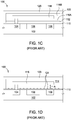
Figures 1A-1D are schematic cross-sectional views of aMEMS device 100 at various stages of fabrication according to the prior art. TheMEMS device 100 includes asubstrate 102 having a plurality ofelectrodes dielectric layer 110 is disposed over thesubstrate 102 andelectrodes - For MEMS that utilize an organic polymer as their sacrificial material, the adhesion of the first layer of the sacrificial material to underlying dielectrics is typically low. In order to fix the low adhesion issue, a silicon polymer is often added to the polymer system. However, the Si, upon removal of the organic sacrificial material, can leave residues behind that can be detrimental to the performance of the MEMS device. As an alternative to adding silicon to the sacrificial material, an independent adhesion promoter material can be used. The adhesion promoter is coated over the substrate, either through a spin-on or CVD type process, prior to the coating of the organic sacrificial material. If inorganic material is used as the sacrificial material, an adhesion promoter would not be utilized.
- An
adhesion promoter layer 112 is then deposited over thedielectric layer 110. Theadhesion promoter layer 112 is used to adhere sacrificial material thereon. A firstsacrificial material layer 116A is then deposited on theadhesion promoter layer 112. The firstsacrificial material layer 116A is an organic sacrificial material comprising carbon, hydrogen, nitrogen and oxygen. The firstsacrificial material layer 116A, theadhesion promoter layer 112 and thedielectric layer 110 are then patterned to expose theelectrode 104. As shown inFigure 1B , an electrical conductive material is then deposited and patterned to form theswitching element 118. A secondsacrificial material layer 116B is then deposited over theswitching element 118. The secondsacrificial material layer 116B and the firstsacrificial material layer 116A are then patterned using standard semiconductor processing techniques. Thecavity 114 is bound by aroof 120,walls 122 and thedielectric layer 110 as shown inFigure 1C . - As shown in
Figure 1D , the first and secondsacrificial material layers adhesion promoter layer 112 are then removed to free theswitching element 118 within thecavity 114 so that theswitching element 118 may move from a position spaced from theelectrode 106 to a position in close proximity to the electrode 106 (i.e., in contact with the dielectric layer 110) as shown by arrow "A". The first and secondsacrificial material layers roof 120 or in through a hole in the side of the cavity. Any silicon contained in the organic sacrificial material would not be etched and would thus remain in the cavity asresidues 124. Theresidues 124 are believed to be remnants of theadhesion promoter layer 112 or silicon that may be present in the sacrificial material. Specifically, silicon present in theadhesion promoter layer 112 or within the sacrificial material may lead to nanoscopic silicon (i.e., silicon with a vacancy in the 1s orbital), which is very prone to charging. Theresidues 124 can interfere with theMEMS device 100 performance by mechanically impeding theswitching element 118 from moving into close proximity to theelectrode 106. The residue can also alter the electrical switching behavior of theMEMS device 100 by storing charge within the silicon that results in a hysteresis loop narrowing, where the difference between the pull-in voltage applied toelectrode 108 which causes the cantilever it be pulled down and that at which the cantilever releases back up, gets smaller.
Therefore, there is a need in the art for a MEMS device and a method for its manufacture in which residues do not interfere with device performance. -
US 5652559 discloses a method of fabricating a MEMS switch wherein a discontinuous Ti layer improves the adhesion of a metal bridge formed thereon. - The present invention generally relates to a MEMS device in which silicon residues from the adhesion promoter material are reduced or even eliminated from the cavity floor. The adhesion promoter is typically used to adhere sacrificial material to the underlying layer. The adhesion promoter is then removed along with the sacrificial material. However, the adhesion promoter leaves silicon based residues within the cavity upon removal. The inventors have discovered that the adhesion promoter can be removed from the cavity area prior to depositing the sacrificial material. The adhesion promoter which remains over the remainder of the substrate is outside of the region where the MEMS device is formed is sufficient to adhere the sacrificial material to the substrate for fabrication of the portion of the MEMS device overlying the electrodes without fear of the sacrificial material delaminating from the substrate. Because no adhesion promoter is used in the cavity area of the device, no silicon residues will be present within the cavity after the switching element of the MEMS device is freed by removing the sacrificial material.
- There is provided a method of fabricating a MEMS device, comprising:
- depositing an adhesion layer over a substrate having a first portion to be enclosed within a cavity and a second portion to be disposed outside the cavity, wherein the adhesion layer comprises silicon;
- removing the adhesion layer in the area disposed over the first portion;
- depositing a sacrificial layer over the adhesion layer and the first portion of the substrate;
- forming a switching element above the sacrificial layer;
- enclosing the switching element within the cavity; and
- removing the sacrificial layer.
- There is also provided a method of fabricating a MEMS device over a substrate having a first portion and a second portion, comprising:
- selectively forming an adhesion layer over the first portion of the substrate, wherein the adhesion layer comprises silicon;
- forming a sacrificial layer over the adhesion layer and the second portion of the substrate;
- forming a switching element over the sacrificial layer and the second portion of the substrate;
- enclosing the switching element within a cavity that is at least partially bound by the second portion of the substrate; and
- removing the sacrificial layer.
- In another embodiment there is provided, a device, comprising:
- a substrate having a first portion at least partially bounding a cavity and a second portion disposed outside the cavity;
- an adhesion layer comprising silicon disposed over the second portion of the substrate, wherein the adhesion layer is not disposed over the first portion; and
- a switching element disposed within the cavity.
- So that the manner in which the above recited features of the present invention can be understood in detail, a more particular description of the invention, briefly summarized above, may be had by reference to embodiments, some of which are illustrated in the appended drawings. It is to be noted, however, that the appended drawings illustrate only typical embodiments of this invention and are therefore not to be considered limiting of its scope, for the invention may admit to other equally effective embodiments.
-
Figures 1A-1D are schematic cross-sectional views of a priorart MEMS device 100 at various stages of production. -
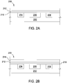
Figures 2A-2G are schematic cross-sectional views of aMEMS device 200 at various stages of production. -
Figures 3A and 3B are examples of switchingelements 222 that may be utilized in the embodiments discussed herein. - To facilitate understanding, identical reference numerals have been used, where possible, to designate identical elements that are common to the figures. It is contemplated that elements disclosed in one embodiment may be beneficially utilized on other embodiments without specific recitation.
- The present invention generally relates to a MEMS device in which silicon residues from the adhesion promoter material are reduced or even eliminated from the cavity floor. The adhesion promoter is typically used to adhere sacrificial material to its underlying layer. The adhesion promoter is then removed along with the sacrificial material. However, the adhesion promoter leaves silicon based residues within the cavity upon removal. As discussed herein, the adhesion promoter can be removed from the cavity area prior to depositing the sacrificial material. The adhesion promoter which remains over the remainder of the substrate is sufficient to adhere the sacrificial material to the substrate without fear of the sacrificial material delaminating. Because no adhesion promoter is used in the cavity area of the device, no silicon residues will be present within the cavity after the switching element of the MEMS device is freed.
-
Figures 2A-2G are schematic cross-sectional views of aMEMS device 200 at various stages of production. As shown inFigure 2A , theMEMS device 200 includes asubstrate 202 having several structures embedded therein. There is anelectrical connection 204 that provides electrical connection from thedevice 200 to layers below thesubstrate 202. There is also a pull-inelectrode 208 that is used to pull the later formed switching element 222 (SeeFigures 2F and 2G ) from a position spaced a first distance from theRF electrode 206 to a second distance closer to theRF electrode 206. Theelectrical connection 204, pull-inelectrode 208 and theRF electrode 206 may all be formed by removing material from thesubstrate 202 by a process such as etching, blanket depositing an electrically conductive material into the etched region of the substrate, and removing excess electrically conductive material from the surface of the substrate by a process such as etching or chemical mechanical polishing. Suitable electrically conductive material that may be used include copper, aluminum, titanium, tungsten, titanium nitride, titanium aluminum nitride, combinations thereof and other well known electrically conductive materials traditionally utilized in the back end of the line (BEOL) of a complementary metal oxide semiconductor (CMOS) manufacturing process. The substrate material that the electrically conductive material is formed within may include electrically insulating material such as silicon oxide, silicon nitride, silicon oxynitride, and combinations thereof. Alternatively, theelectrical connection 204, pull-inelectrode 208 and theRF electrode 206 may all be formed by first blanket depositing an electrically conductive material over thesubstrate 202. Thereafter, excess portions of the electrically conductive material are removed by a process such as etching to form the final shape of theelectrical connection 204, pull-inelectrode 208 and theRF electrode 206. - As shown in
Figure 2A , an electrically insulatinglayer 210, followed byadhesion promoter layer 212, may be deposited over the exposedsubstrate 202 andelectrical connection 204, pull-inelectrode 208 and theRF electrode 206 by a blanket deposition process. Excess electrically insulating material may then be removed by a process such as etching or CMP. The electrically insulatinglayer 210 prevents shorting between the switchingelement 222 and the pull-inelectrode 208. - The
adhesion promoter layer 212 is then deposited over the electrically insulatinglayer 210. Theadhesion promoter layer 212 may be deposited to a thickness of less than 20 nm, such as between about 4 nm and about 20 nm, or about 6 nm. Suitable materials that may be utilized for theadhesion promoter layer 212 include a compound comprising silicon covalently bonded to an organic functionality, such as AP3000, AP4000and AP6300 which are available from Dow Chemical, which are, in general, organoxilane based to form the correct bonding termination between SiO2 and the organic sacrificial material. Theadhesion promoter layer 212 is tailored to the specific film that requires improved adhesion. In general, theadhesion promoter layer 212 contains about 29 atomic percent silicon, with an upper limit of 30 atomic percent silicon. Theadhesion promoter layer 212 is utilized to adhere thesacrificial layer 220 to thedevice 200. In the absence of theadhesion promoter layer 212, thesacrificial layer 220 would delaminate from thedevice 200. Theadhesion promoter layer 212 may be deposited by a spin-on process. - As discussed above, the
adhesion promoter layer 212 can be the source of residues within thecavity 226. Thus, theadhesion promoter layer 212 is removed from thecavity 226 prior to depositing thesacrificial layer 220. Theadhesion promoter layer 212 will remain over thesubstrate 202 in the areas outside of thecavity 226. It is to be understood that some residualadhesion promoter layer 212 may remain within thecavity 226 even after the removal process. The residualadhesion promoter layer 212 should not be under the MEMS area or even the MEMS touchdown area of theswitching element 222 so that if any residues form, the residues do not alter the landing properties of the MEMS device. In order to remove theadhesion promoter layer 212, aphotoresist layer 214 is deposited over theadhesion promoter layer 212 as shown inFigure 2B and then patterned to form amask 216 as shown inFigure 2C . The opening in themask 216 corresponds to the portions of theadhesion promoter layer 212 that will be removed prior to deposition of the sacrificial material. The exposedadhesion promoter layer 212 is etched to leave a pattern on the substrate ofadhesion promoter layer 218 in the areas outside the region of theelectrodes adhesion promoter layer 212 within the region ofelectrodes Figure 2D . The remaining, patternedadhesion promoter layer 218 will be sufficient to adhere thesacrificial layer 220 to thesubstrate 202 without permitting thesacrificial layer 220 to delaminate before formation of a switching element (SeeFigure 2F ). If theadhesion promoter layer 212 were to remain over theelectrodes - In absence of the patterned
adhesion promoter layer 218, thesacrificial layer 220 would delaminate over the large area of thesubstrate 202 when thesacrificial layer 220 is wet-processed. The area of the un-patternedadhesion promoter layer 218 is sufficiently large as compared to thecavity 226 that the remainingadhesion promoter layer 218 will hold down thesacrificial layer 220 over the remaining portions of the wafer. - Once the patterned
adhesion promoter layer 218 is formed, themask 216 is removed by a well known process such as ashing or wet etching, and thesacrificial layer 220 is deposited as shown inFigure 2E . Suitable materials that may be used for thesacrificial layer 220 include on organic based dielectric containing a long chain molecule with a carbon backbone. Specific materials that may be used for thesacrificial layer 220 includes polyarylene or polyphenylene based polymers such as SILK™ available from Dow Chemical or the LKD 7200 series from JSR. The organic functionality of the patternedadhesion promoter layer 218 provides the necessary bonding functionality for thesacrificial layer 220. Thesacrificial layer 220 may be deposited by a spin-on process and then cured. The patternedadhesion promoter layer 218 provides adequate adhesion for the spin-onsacrificial layer 220 to permit thesacrificial layer 220 to survive the remainder of theMEMS device 200 process steps. Once thesacrificial layer 220 is deposited, it is patterned and the remainder of thedevice 200 is formed. - A switching
element 222 is formed over thesacrificial layer 220 and anothersacrificial layer 224 is formed over the switchingelement 222 to embed theswitching element 222 within sacrificial material. No extra adhesion layer is required at this stage as most of the second sacrificial layer lies on the first sacrificial layer, however if an adhesion layer was required, such an adhesion layer could be patterned so as not to remain in the cavity area. The switchingelement 222 is formed by blanket depositing an electrically conductive material, forming a mask thereover, etching the electrically conductive material to form theswitching element 222, and then removing the mask by a well known process such as ashing or etching. The switchingelement 222 is electrically connected toelectrical connection 204. - Once all of the sacrificial material has been deposited and patterned to define the interior shape of the
cavity 226, thecavity 226 may be encapsulated such that aroof 228 andwalls 230 are present as shown inFigure 2F . An opening may be formed through one or more of theroof 228 and thewalls 230 in order to introduce an etchant that will remove thesacrificial layers element 222 to move within thecavity 226. Thesacrificial layers Figure 2G , because theadhesion promoter layer 212 was removed from thecavity 226 prior to depositing thesacrificial layer 220, there are no residues within thecavity 226 and the switching element is not obstructed by residues or repulsive charging of the electrically insulatinglayer 210. - It is to be understood that while the
switching element 222 has been shown as a cantilever structure having a free end and a fixed end that is coupled to theelectrical connection 204, the invention is not restricted to such a switching element. The invention is equally applicable to other switching elements such as a switching element that is fixed at opposite ends with an electrical connection at the ends and a flexible bridge between the fixed ends that is movable between a position spaced from an RF electrode and a position is close proximity to the RF electrode. Suitable materials that may be used for theswitching element 222 include titanium nitride, titanium aluminum, tungsten, copper, titanium aluminum nitride aluminum and combinations thereof and multilayer structures such as titanium nitride-aluminum-titanium nitride or an oxide-titanium aluminum nitride-oxide stack. The switchingelement 222 may be formed by depositing electrically conductive material by a method such as physical vapor deposition (PVD) and then patterning the electrically conductive material by a process such as etching. If desired, an electrically insulating material may be formed on one or more of the top surface and the bottom surface of theswitching element 222. -
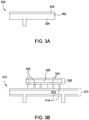
Figures 3A and 3B are examples of switchingelements 222 that may be utilized in the embodiments discussed herein. InFigure 3A , the switchingelement 222 includes a plurality ofdielectric layers 304 that at least partially encapsulate theconductive portion 302 of theswitching element 222. Thedielectric layers 304 are thinner than theconductive portion 302. Thedielectric layers 304 are beneficial because the sacrificial material would otherwise interact with exposed conductive material to produce non-volatile residues which would remain in thecavity 226. When theconductive portion 302 are at least partially isolated from thecavity 226 by encapsulating them with dielectric layers 304 (e.g., oxide material such as silicon dioxide), the amount of post release residue is significantly decreased or eliminated altogether. -
Figure 3B shows aswitching element 222 according to another embodiment. The switchingelement 222 has a waffle-like structure in which abottom portion 310 is coupled to atop portion 320 by one or more electricallyconductive posts 330. Thebottom portion 310 includes aconductive portion 312 that is surrounded by a plurality ofdielectric layers 314 that at least partially encapsulate theconductive portion 312. Similarly, thetop portion 320 includes aconductive portion 322 that is surrounded by a plurality ofdielectric layers 324 that at least partially encapsulate theconductive portion 322. - By utilizing an adhesion promoter layer in the areas of the MEMS device that are outside of the device cavity, the sacrificial layer may be deposited and adhered without fear of delimitation during further MEMS processing. Without the silicon based adhesion layer within the cavity, silicon residues are reduced or even eliminated. Thus, the MEMS device may be fabricated with the necessary sacrificial material without fear of the sacrificial material delaminating or adhesion material residue interfering with mechanical or electrical operation of the MEMS device.
- It is to be understood that the adhesion promoter layer may be removed and/or not present within the cavity area according to other methods as well. For example, it is contemplated that a mask may be formed over the dielectric layer. The mask has the desired shape of the bottom of the cavity. The adhesion promoter is then blanket deposited over the substrate. The mask, with adhesion promoter material thereon, is then removed such that the desired areas do not have adhesion promoter thereover.
- While the foregoing is directed to embodiments of the present invention, other and further embodiments of the invention may be devised without departing from the basic scope thereof, and the scope thereof is determined by the claims that follow.
Claims (19)
- A method of fabricating a MEMS device, comprising:depositing an adhesion layer over a substrate having a first portion to be enclosed within a cavity and a second portion to be disposed outside the cavity, wherein the adhesion layer comprises silicon;removing the adhesion layer in the area disposed over the first portion;depositing a sacrificial layer over the adhesion layer and the first portion of the substrate;forming a switching element above the sacrificial layer;enclosing the switching element within the cavity; andremoving the sacrificial layer.
- The method of claim 1, wherein the sacrificial layer comprises a dielectric material.
- The method of claim 2, wherein the dielectric material is an organic dielectric material.
- The method of claim 1, wherein removing the adhesion layer comprises:depositing a photoresist layer over the adhesion layer;exposing select areas the photoresist layer that correspond to the first portion of the substrate;developing the photoresist layer to remove the select areas of the photoresist layer and thereby form a mask and expose the adhesion layer in the area disposed over the first portionetching the exposed adhesion layer.
- The method of claim 4, further comprising depositing an electrically insulating layer over the substrate prior to depositing the adhesion layer.
- The method of claim 1, wherein the adhesion layer comprises silicon covalently bonded to an organic material.
- A method of fabricating a MEMS device over a substrate having a first portion and a second portion, comprising:selectively forming an adhesion layer over the first portion of the substrate, wherein the adhesion layer comprises silicon;forming a sacrificial layer over the adhesion layer and the second portion of the substrate;forming a switching element over the sacrificial layer and the second portion of the substrate;enclosing the switching element within a cavity that is at least partially bound by the second portion of the substrate; andremoving the sacrificial layer.
- The method of claim 7, wherein the sacrificial layer comprises a dielectric material.
- The method of claim 8, wherein the dielectric material is an organic dielectric material.
- The method of claim 9, further comprising depositing an electrically insulating layer over the substrate prior to selectively forming the adhesion layer.
- The method of claim 7, further comprising depositing an electrically insulating layer over the substrate prior to depositing the adhesion layer.
- The method of claim 7, wherein the adhesion layer comprises silicon covalently bonded to an organic material.
- A device, comprising:a substrate having a first portion at least partially bounding a cavity and a second portion disposed outside the cavity;an adhesion layer comprising silicon disposed over the second portion of the substrate, wherein the adhesion layer is not disposed over the first portion; anda switching element disposed within the cavity.
- The device of claim 13, wherein the device is a MEMS device.
- The device of claim 14, wherein the adhesion layer comprises silicon covalently bonded to an organic material.
- The device of claim 15, further comprising an electrically insulating layer disposed on the substrate, wherein the adhesion layer is disposed on the electrically insulating layer.
- The device of claim 16, wherein the adhesion layer comprises silicon covalently bonded to an organic material.
- The device of claim 13, further comprising a dielectric layer disposed on the substrate, wherein the adhesion layer is disposed on the dielectric layer.
- The device of claim 13, wherein the switching element is at least partially encapsulated in dielectric material.
Applications Claiming Priority (3)
| Application Number | Priority Date | Filing Date | Title |
|---|---|---|---|
| US201161514823P | 2011-08-03 | 2011-08-03 | |
| US13/565,693 US8921165B2 (en) | 2011-08-03 | 2012-08-02 | Elimination of silicon residues from MEMS cavity floor |
| PCT/US2012/049497 WO2013020039A2 (en) | 2011-08-03 | 2012-08-03 | Elimination of silicon residues from mems cavity floor |
Publications (2)
| Publication Number | Publication Date |
|---|---|
| EP2739562A2 EP2739562A2 (en) | 2014-06-11 |
| EP2739562B1 true EP2739562B1 (en) | 2017-12-20 |
Family
ID=47626256
Family Applications (1)
| Application Number | Title | Priority Date | Filing Date |
|---|---|---|---|
| EP12746449.3A Active EP2739562B1 (en) | 2011-08-03 | 2012-08-03 | Elimination of silicon residues from mems cavity floor |
Country Status (6)
| Country | Link |
|---|---|
| US (1) | US8921165B2 (en) |
| EP (1) | EP2739562B1 (en) |
| JP (1) | JP6021914B2 (en) |
| KR (1) | KR101937767B1 (en) |
| CN (1) | CN103732528B (en) |
| WO (1) | WO2013020039A2 (en) |
Families Citing this family (2)
| Publication number | Priority date | Publication date | Assignee | Title |
|---|---|---|---|---|
| KR102654319B1 (en) * | 2015-11-16 | 2024-04-04 | 코르보 유에스, 인크. | Current handling in the legs and anchors of an RF switch |
| EP3929540A1 (en) * | 2020-06-26 | 2021-12-29 | TE Connectivity Norge AS | Attachment system for attaching a sensor to a substrate, method of attaching a sensor to a substrate |
Family Cites Families (17)
| Publication number | Priority date | Publication date | Assignee | Title |
|---|---|---|---|---|
| US5531018A (en) * | 1993-12-20 | 1996-07-02 | General Electric Company | Method of micromachining electromagnetically actuated current switches with polyimide reinforcement seals, and switches produced thereby |
| US5994161A (en) * | 1997-09-03 | 1999-11-30 | Motorola, Inc. | Temperature coefficient of offset adjusted semiconductor device and method thereof |
| GB0011964D0 (en) * | 2000-05-18 | 2000-07-05 | Suyal N | Thick glass films with controlled refractive indices and their applications |
| EP1251577B1 (en) * | 2001-04-19 | 2007-04-25 | Interuniversitair Microelektronica Centrum Vzw | Fabrication of integrated tunable/switchable passive microwave and millimeter wave modules |
| US6798029B2 (en) * | 2003-05-09 | 2004-09-28 | International Business Machines Corporation | Method of fabricating micro-electromechanical switches on CMOS compatible substrates |
| US7148436B1 (en) * | 2003-08-14 | 2006-12-12 | Sandia Corporation | Microelectromechanical acceleration-sensing apparatus |
| TW593127B (en) * | 2003-08-18 | 2004-06-21 | Prime View Int Co Ltd | Interference display plate and manufacturing method thereof |
| JP2006231439A (en) * | 2005-02-23 | 2006-09-07 | Sony Corp | Fine mechanical element and its manufacturing method, semiconductor device and communication equipment |
| JP4807987B2 (en) * | 2005-09-06 | 2011-11-02 | 日本電信電話株式会社 | Hermetically sealed package and optical submodule |
| CN101360849B (en) * | 2005-11-18 | 2013-05-15 | 莱里斯奥鲁斯集团 | Method for forming multi-layer structure |
| KR20080097023A (en) * | 2007-04-30 | 2008-11-04 | 엘지전자 주식회사 | Rf mems switch and fabrication method thereof |
| JP2009009884A (en) * | 2007-06-29 | 2009-01-15 | Mitsubishi Electric Corp | Mems switch, and manufacturing method thereof |
| CN101572850A (en) * | 2008-04-11 | 2009-11-04 | 王文 | Capacitance type microphone with stress release membrane prepared at a low temperature and preparation method thereof |
| JP4636292B2 (en) * | 2008-08-27 | 2011-02-23 | 株式会社村田製作所 | Electronic component and method for manufacturing electronic component |
| CN101738865A (en) * | 2008-11-05 | 2010-06-16 | 中芯国际集成电路制造(上海)有限公司 | Dry-method film coating process |
| CN101800189B (en) * | 2009-02-11 | 2013-05-01 | 中国科学院微电子研究所 | Method for manufacturing medium bridge by utilizing benzocyclobutene |
| US8289674B2 (en) | 2009-03-17 | 2012-10-16 | Cavendish Kinetics, Ltd. | Moving a free-standing structure between high and low adhesion states |
-
2012
- 2012-08-02 US US13/565,693 patent/US8921165B2/en active Active
- 2012-08-03 KR KR1020147005594A patent/KR101937767B1/en active IP Right Grant
- 2012-08-03 WO PCT/US2012/049497 patent/WO2013020039A2/en active Application Filing
- 2012-08-03 EP EP12746449.3A patent/EP2739562B1/en active Active
- 2012-08-03 JP JP2014524104A patent/JP6021914B2/en active Active
- 2012-08-03 CN CN201280038717.4A patent/CN103732528B/en active Active
Also Published As
| Publication number | Publication date |
|---|---|
| US20130032453A1 (en) | 2013-02-07 |
| JP2014521527A (en) | 2014-08-28 |
| CN103732528A (en) | 2014-04-16 |
| WO2013020039A2 (en) | 2013-02-07 |
| WO2013020039A3 (en) | 2013-03-21 |
| US8921165B2 (en) | 2014-12-30 |
| EP2739562A2 (en) | 2014-06-11 |
| JP6021914B2 (en) | 2016-11-09 |
| KR20140053263A (en) | 2014-05-07 |
| CN103732528B (en) | 2018-09-28 |
| KR101937767B1 (en) | 2019-04-11 |
Similar Documents
| Publication | Publication Date | Title |
|---|---|---|
| US7993950B2 (en) | System and method of encapsulation | |
| KR101939175B1 (en) | Mems device anchoring | |
| US9711291B2 (en) | MEMS digital variable capacitor design with high linearity | |
| EP2542499B1 (en) | Cmp process flow for mems | |
| EP2739562B1 (en) | Elimination of silicon residues from mems cavity floor | |
| US8921953B2 (en) | Method for MEMS device fabrication and device formed | |
| US9162877B2 (en) | Lateral etch stop for NEMS release etch for high density NEMS/CMOS monolithic integration | |
| EP3052429B1 (en) | Method for achieving good adhesion between dielectric and organic material | |
| CN112447587B (en) | Method for manufacturing interconnect structure |
Legal Events
| Date | Code | Title | Description |
|---|---|---|---|
| PUAI | Public reference made under article 153(3) epc to a published international application that has entered the european phase |
Free format text: ORIGINAL CODE: 0009012 |
|
| 17P | Request for examination filed |
Effective date: 20140204 |
|
| AK | Designated contracting states |
Kind code of ref document: A2 Designated state(s): AL AT BE BG CH CY CZ DE DK EE ES FI FR GB GR HR HU IE IS IT LI LT LU LV MC MK MT NL NO PL PT RO RS SE SI SK SM TR |
|
| DAX | Request for extension of the european patent (deleted) | ||
| REG | Reference to a national code |
Ref country code: DE Ref legal event code: R079 Ref document number: 602012041107 Country of ref document: DE Free format text: PREVIOUS MAIN CLASS: B81C0001000000 Ipc: B81B0003000000 |
|
| GRAP | Despatch of communication of intention to grant a patent |
Free format text: ORIGINAL CODE: EPIDOSNIGR1 |
|
| RIC1 | Information provided on ipc code assigned before grant |
Ipc: B81C 1/00 20060101ALI20170612BHEP Ipc: H01H 1/00 20060101ALI20170612BHEP Ipc: B81B 3/00 20060101AFI20170612BHEP |
|
| INTG | Intention to grant announced |
Effective date: 20170718 |
|
| RAP1 | Party data changed (applicant data changed or rights of an application transferred) |
Owner name: CAVENDISH KINETICS, INC. |
|
| GRAS | Grant fee paid |
Free format text: ORIGINAL CODE: EPIDOSNIGR3 |
|
| GRAA | (expected) grant |
Free format text: ORIGINAL CODE: 0009210 |
|
| AK | Designated contracting states |
Kind code of ref document: B1 Designated state(s): AL AT BE BG CH CY CZ DE DK EE ES FI FR GB GR HR HU IE IS IT LI LT LU LV MC MK MT NL NO PL PT RO RS SE SI SK SM TR |
|
| REG | Reference to a national code |
Ref country code: GB Ref legal event code: FG4D |
|
| REG | Reference to a national code |
Ref country code: CH Ref legal event code: EP |
|
| REG | Reference to a national code |
Ref country code: IE Ref legal event code: FG4D |
|
| REG | Reference to a national code |
Ref country code: AT Ref legal event code: REF Ref document number: 956181 Country of ref document: AT Kind code of ref document: T Effective date: 20180115 |
|
| REG | Reference to a national code |
Ref country code: DE Ref legal event code: R096 Ref document number: 602012041107 Country of ref document: DE |
|
| REG | Reference to a national code |
Ref country code: NL Ref legal event code: MP Effective date: 20171220 |
|
| PG25 | Lapsed in a contracting state [announced via postgrant information from national office to epo] |
Ref country code: LT Free format text: LAPSE BECAUSE OF FAILURE TO SUBMIT A TRANSLATION OF THE DESCRIPTION OR TO PAY THE FEE WITHIN THE PRESCRIBED TIME-LIMIT Effective date: 20171220 Ref country code: FI Free format text: LAPSE BECAUSE OF FAILURE TO SUBMIT A TRANSLATION OF THE DESCRIPTION OR TO PAY THE FEE WITHIN THE PRESCRIBED TIME-LIMIT Effective date: 20171220 Ref country code: NO Free format text: LAPSE BECAUSE OF FAILURE TO SUBMIT A TRANSLATION OF THE DESCRIPTION OR TO PAY THE FEE WITHIN THE PRESCRIBED TIME-LIMIT Effective date: 20180320 Ref country code: SE Free format text: LAPSE BECAUSE OF FAILURE TO SUBMIT A TRANSLATION OF THE DESCRIPTION OR TO PAY THE FEE WITHIN THE PRESCRIBED TIME-LIMIT Effective date: 20171220 |
|
| REG | Reference to a national code |
Ref country code: LT Ref legal event code: MG4D |
|
| REG | Reference to a national code |
Ref country code: AT Ref legal event code: MK05 Ref document number: 956181 Country of ref document: AT Kind code of ref document: T Effective date: 20171220 |
|
| PG25 | Lapsed in a contracting state [announced via postgrant information from national office to epo] |
Ref country code: GR Free format text: LAPSE BECAUSE OF FAILURE TO SUBMIT A TRANSLATION OF THE DESCRIPTION OR TO PAY THE FEE WITHIN THE PRESCRIBED TIME-LIMIT Effective date: 20180321 Ref country code: LV Free format text: LAPSE BECAUSE OF FAILURE TO SUBMIT A TRANSLATION OF THE DESCRIPTION OR TO PAY THE FEE WITHIN THE PRESCRIBED TIME-LIMIT Effective date: 20171220 Ref country code: BG Free format text: LAPSE BECAUSE OF FAILURE TO SUBMIT A TRANSLATION OF THE DESCRIPTION OR TO PAY THE FEE WITHIN THE PRESCRIBED TIME-LIMIT Effective date: 20180320 Ref country code: HR Free format text: LAPSE BECAUSE OF FAILURE TO SUBMIT A TRANSLATION OF THE DESCRIPTION OR TO PAY THE FEE WITHIN THE PRESCRIBED TIME-LIMIT Effective date: 20171220 Ref country code: RS Free format text: LAPSE BECAUSE OF FAILURE TO SUBMIT A TRANSLATION OF THE DESCRIPTION OR TO PAY THE FEE WITHIN THE PRESCRIBED TIME-LIMIT Effective date: 20171220 |
|
| REG | Reference to a national code |
Ref country code: FR Ref legal event code: PLFP Year of fee payment: 7 |
|
| PG25 | Lapsed in a contracting state [announced via postgrant information from national office to epo] |
Ref country code: NL Free format text: LAPSE BECAUSE OF FAILURE TO SUBMIT A TRANSLATION OF THE DESCRIPTION OR TO PAY THE FEE WITHIN THE PRESCRIBED TIME-LIMIT Effective date: 20171220 |
|
| PG25 | Lapsed in a contracting state [announced via postgrant information from national office to epo] |
Ref country code: CZ Free format text: LAPSE BECAUSE OF FAILURE TO SUBMIT A TRANSLATION OF THE DESCRIPTION OR TO PAY THE FEE WITHIN THE PRESCRIBED TIME-LIMIT Effective date: 20171220 Ref country code: SK Free format text: LAPSE BECAUSE OF FAILURE TO SUBMIT A TRANSLATION OF THE DESCRIPTION OR TO PAY THE FEE WITHIN THE PRESCRIBED TIME-LIMIT Effective date: 20171220 Ref country code: EE Free format text: LAPSE BECAUSE OF FAILURE TO SUBMIT A TRANSLATION OF THE DESCRIPTION OR TO PAY THE FEE WITHIN THE PRESCRIBED TIME-LIMIT Effective date: 20171220 Ref country code: CY Free format text: LAPSE BECAUSE OF FAILURE TO SUBMIT A TRANSLATION OF THE DESCRIPTION OR TO PAY THE FEE WITHIN THE PRESCRIBED TIME-LIMIT Effective date: 20171220 Ref country code: ES Free format text: LAPSE BECAUSE OF FAILURE TO SUBMIT A TRANSLATION OF THE DESCRIPTION OR TO PAY THE FEE WITHIN THE PRESCRIBED TIME-LIMIT Effective date: 20171220 |
|
| PG25 | Lapsed in a contracting state [announced via postgrant information from national office to epo] |
Ref country code: IS Free format text: LAPSE BECAUSE OF FAILURE TO SUBMIT A TRANSLATION OF THE DESCRIPTION OR TO PAY THE FEE WITHIN THE PRESCRIBED TIME-LIMIT Effective date: 20180420 Ref country code: RO Free format text: LAPSE BECAUSE OF FAILURE TO SUBMIT A TRANSLATION OF THE DESCRIPTION OR TO PAY THE FEE WITHIN THE PRESCRIBED TIME-LIMIT Effective date: 20171220 Ref country code: AT Free format text: LAPSE BECAUSE OF FAILURE TO SUBMIT A TRANSLATION OF THE DESCRIPTION OR TO PAY THE FEE WITHIN THE PRESCRIBED TIME-LIMIT Effective date: 20171220 Ref country code: SM Free format text: LAPSE BECAUSE OF FAILURE TO SUBMIT A TRANSLATION OF THE DESCRIPTION OR TO PAY THE FEE WITHIN THE PRESCRIBED TIME-LIMIT Effective date: 20171220 Ref country code: IT Free format text: LAPSE BECAUSE OF FAILURE TO SUBMIT A TRANSLATION OF THE DESCRIPTION OR TO PAY THE FEE WITHIN THE PRESCRIBED TIME-LIMIT Effective date: 20171220 Ref country code: PL Free format text: LAPSE BECAUSE OF FAILURE TO SUBMIT A TRANSLATION OF THE DESCRIPTION OR TO PAY THE FEE WITHIN THE PRESCRIBED TIME-LIMIT Effective date: 20171220 |
|
| REG | Reference to a national code |
Ref country code: DE Ref legal event code: R097 Ref document number: 602012041107 Country of ref document: DE |
|
| PLBE | No opposition filed within time limit |
Free format text: ORIGINAL CODE: 0009261 |
|
| STAA | Information on the status of an ep patent application or granted ep patent |
Free format text: STATUS: NO OPPOSITION FILED WITHIN TIME LIMIT |
|
| 26N | No opposition filed |
Effective date: 20180921 |
|
| PG25 | Lapsed in a contracting state [announced via postgrant information from national office to epo] |
Ref country code: DK Free format text: LAPSE BECAUSE OF FAILURE TO SUBMIT A TRANSLATION OF THE DESCRIPTION OR TO PAY THE FEE WITHIN THE PRESCRIBED TIME-LIMIT Effective date: 20171220 |
|
| PG25 | Lapsed in a contracting state [announced via postgrant information from national office to epo] |
Ref country code: SI Free format text: LAPSE BECAUSE OF FAILURE TO SUBMIT A TRANSLATION OF THE DESCRIPTION OR TO PAY THE FEE WITHIN THE PRESCRIBED TIME-LIMIT Effective date: 20171220 |
|
| PG25 | Lapsed in a contracting state [announced via postgrant information from national office to epo] |
Ref country code: MC Free format text: LAPSE BECAUSE OF FAILURE TO SUBMIT A TRANSLATION OF THE DESCRIPTION OR TO PAY THE FEE WITHIN THE PRESCRIBED TIME-LIMIT Effective date: 20171220 |
|
| REG | Reference to a national code |
Ref country code: CH Ref legal event code: PL |
|
| PG25 | Lapsed in a contracting state [announced via postgrant information from national office to epo] |
Ref country code: LU Free format text: LAPSE BECAUSE OF NON-PAYMENT OF DUE FEES Effective date: 20180803 Ref country code: LI Free format text: LAPSE BECAUSE OF NON-PAYMENT OF DUE FEES Effective date: 20180831 Ref country code: CH Free format text: LAPSE BECAUSE OF NON-PAYMENT OF DUE FEES Effective date: 20180831 |
|
| REG | Reference to a national code |
Ref country code: BE Ref legal event code: MM Effective date: 20180831 |
|
| REG | Reference to a national code |
Ref country code: IE Ref legal event code: MM4A |
|
| PG25 | Lapsed in a contracting state [announced via postgrant information from national office to epo] |
Ref country code: IE Free format text: LAPSE BECAUSE OF NON-PAYMENT OF DUE FEES Effective date: 20180803 |
|
| PG25 | Lapsed in a contracting state [announced via postgrant information from national office to epo] |
Ref country code: BE Free format text: LAPSE BECAUSE OF NON-PAYMENT OF DUE FEES Effective date: 20180831 |
|
| PG25 | Lapsed in a contracting state [announced via postgrant information from national office to epo] |
Ref country code: MT Free format text: LAPSE BECAUSE OF NON-PAYMENT OF DUE FEES Effective date: 20180803 |
|
| PG25 | Lapsed in a contracting state [announced via postgrant information from national office to epo] |
Ref country code: TR Free format text: LAPSE BECAUSE OF FAILURE TO SUBMIT A TRANSLATION OF THE DESCRIPTION OR TO PAY THE FEE WITHIN THE PRESCRIBED TIME-LIMIT Effective date: 20171220 |
|
| PG25 | Lapsed in a contracting state [announced via postgrant information from national office to epo] |
Ref country code: HU Free format text: LAPSE BECAUSE OF FAILURE TO SUBMIT A TRANSLATION OF THE DESCRIPTION OR TO PAY THE FEE WITHIN THE PRESCRIBED TIME-LIMIT; INVALID AB INITIO Effective date: 20120803 Ref country code: PT Free format text: LAPSE BECAUSE OF FAILURE TO SUBMIT A TRANSLATION OF THE DESCRIPTION OR TO PAY THE FEE WITHIN THE PRESCRIBED TIME-LIMIT Effective date: 20171220 |
|
| PG25 | Lapsed in a contracting state [announced via postgrant information from national office to epo] |
Ref country code: MK Free format text: LAPSE BECAUSE OF NON-PAYMENT OF DUE FEES Effective date: 20171220 |
|
| PG25 | Lapsed in a contracting state [announced via postgrant information from national office to epo] |
Ref country code: AL Free format text: LAPSE BECAUSE OF FAILURE TO SUBMIT A TRANSLATION OF THE DESCRIPTION OR TO PAY THE FEE WITHIN THE PRESCRIBED TIME-LIMIT Effective date: 20171220 |
|
| REG | Reference to a national code |
Ref country code: GB Ref legal event code: 732E Free format text: REGISTERED BETWEEN 20220505 AND 20220512 |
|
| REG | Reference to a national code |
Ref country code: DE Ref legal event code: R081 Ref document number: 602012041107 Country of ref document: DE Owner name: QORVO US, INC., GREENSBORO, US Free format text: FORMER OWNER: CAVENDISH KINETICS INC., SAN JOSE, CALIF., US |
|
| PGFP | Annual fee paid to national office [announced via postgrant information from national office to epo] |
Ref country code: GB Payment date: 20230720 Year of fee payment: 12 |
|
| PGFP | Annual fee paid to national office [announced via postgrant information from national office to epo] |
Ref country code: FR Payment date: 20230720 Year of fee payment: 12 Ref country code: DE Payment date: 20230720 Year of fee payment: 12 |