EP2738770B1 - Low resistance area magnetic stack - Google Patents
Low resistance area magnetic stack Download PDFInfo
- Publication number
- EP2738770B1 EP2738770B1 EP13195190.7A EP13195190A EP2738770B1 EP 2738770 B1 EP2738770 B1 EP 2738770B1 EP 13195190 A EP13195190 A EP 13195190A EP 2738770 B1 EP2738770 B1 EP 2738770B1
- Authority
- EP
- European Patent Office
- Prior art keywords
- layer
- layers
- binary compound
- alloy
- magnetic
- Prior art date
- Legal status (The legal status is an assumption and is not a legal conclusion. Google has not performed a legal analysis and makes no representation as to the accuracy of the status listed.)
- Not-in-force
Links
- 230000005291 magnetic effect Effects 0.000 title claims description 58
- 230000004888 barrier function Effects 0.000 claims description 62
- 229910045601 alloy Inorganic materials 0.000 claims description 53
- 239000000956 alloy Substances 0.000 claims description 53
- 150000001875 compounds Chemical class 0.000 claims description 47
- 229910052751 metal Inorganic materials 0.000 claims description 42
- 239000002184 metal Substances 0.000 claims description 42
- 230000005294 ferromagnetic effect Effects 0.000 claims description 23
- 239000000463 material Substances 0.000 claims description 19
- 230000005415 magnetization Effects 0.000 claims description 13
- 238000000151 deposition Methods 0.000 claims description 9
- 239000011777 magnesium Substances 0.000 claims description 9
- 238000000034 method Methods 0.000 claims description 8
- 239000000203 mixture Substances 0.000 claims description 8
- 229910052788 barium Inorganic materials 0.000 claims description 7
- 229910052744 lithium Inorganic materials 0.000 claims description 7
- 229910052712 strontium Inorganic materials 0.000 claims description 7
- 238000003475 lamination Methods 0.000 claims description 6
- WHXSMMKQMYFTQS-UHFFFAOYSA-N Lithium Chemical compound [Li] WHXSMMKQMYFTQS-UHFFFAOYSA-N 0.000 claims description 3
- QVGXLLKOCUKJST-UHFFFAOYSA-N atomic oxygen Chemical compound [O] QVGXLLKOCUKJST-UHFFFAOYSA-N 0.000 claims description 3
- DSAJWYNOEDNPEQ-UHFFFAOYSA-N barium atom Chemical compound [Ba] DSAJWYNOEDNPEQ-UHFFFAOYSA-N 0.000 claims description 3
- 238000001816 cooling Methods 0.000 claims description 3
- 229910052749 magnesium Inorganic materials 0.000 claims description 3
- 229910052760 oxygen Inorganic materials 0.000 claims description 3
- 239000001301 oxygen Substances 0.000 claims description 3
- CIOAGBVUUVVLOB-UHFFFAOYSA-N strontium atom Chemical compound [Sr] CIOAGBVUUVVLOB-UHFFFAOYSA-N 0.000 claims description 3
- FYYHWMGAXLPEAU-UHFFFAOYSA-N Magnesium Chemical compound [Mg] FYYHWMGAXLPEAU-UHFFFAOYSA-N 0.000 claims description 2
- 238000010438 heat treatment Methods 0.000 claims description 2
- CPLXHLVBOLITMK-UHFFFAOYSA-N Magnesium oxide Chemical compound [Mg]=O CPLXHLVBOLITMK-UHFFFAOYSA-N 0.000 description 17
- 238000013500 data storage Methods 0.000 description 11
- 239000000395 magnesium oxide Substances 0.000 description 9
- 238000003860 storage Methods 0.000 description 5
- 230000002463 transducing effect Effects 0.000 description 5
- 229910052784 alkaline earth metal Inorganic materials 0.000 description 4
- 150000001342 alkaline earth metals Chemical class 0.000 description 4
- 239000007772 electrode material Substances 0.000 description 4
- 239000007769 metal material Substances 0.000 description 4
- 230000015572 biosynthetic process Effects 0.000 description 3
- 230000008021 deposition Effects 0.000 description 3
- 238000004519 manufacturing process Methods 0.000 description 3
- 230000005641 tunneling Effects 0.000 description 3
- 230000008901 benefit Effects 0.000 description 2
- 229910052802 copper Inorganic materials 0.000 description 2
- 239000010949 copper Substances 0.000 description 2
- 230000008878 coupling Effects 0.000 description 2
- 238000010168 coupling process Methods 0.000 description 2
- 238000005859 coupling reaction Methods 0.000 description 2
- 239000013078 crystal Substances 0.000 description 2
- 230000007547 defect Effects 0.000 description 2
- 238000011282 treatment Methods 0.000 description 2
- ZOXJGFHDIHLPTG-UHFFFAOYSA-N Boron Chemical compound [B] ZOXJGFHDIHLPTG-UHFFFAOYSA-N 0.000 description 1
- RYGMFSIKBFXOCR-UHFFFAOYSA-N Copper Chemical compound [Cu] RYGMFSIKBFXOCR-UHFFFAOYSA-N 0.000 description 1
- 229910002056 binary alloy Inorganic materials 0.000 description 1
- 229910052796 boron Inorganic materials 0.000 description 1
- 238000010276 construction Methods 0.000 description 1
- 238000001514 detection method Methods 0.000 description 1
- 238000005421 electrostatic potential Methods 0.000 description 1
- 238000005516 engineering process Methods 0.000 description 1
- 230000004907 flux Effects 0.000 description 1
- 238000011065 in-situ storage Methods 0.000 description 1
- AXZKOIWUVFPNLO-UHFFFAOYSA-N magnesium;oxygen(2-) Chemical compound [O-2].[Mg+2] AXZKOIWUVFPNLO-UHFFFAOYSA-N 0.000 description 1
- 239000000696 magnetic material Substances 0.000 description 1
- 238000005457 optimization Methods 0.000 description 1
- 230000003647 oxidation Effects 0.000 description 1
- 238000007254 oxidation reaction Methods 0.000 description 1
- 230000008569 process Effects 0.000 description 1
- 230000001737 promoting effect Effects 0.000 description 1
- 238000004544 sputter deposition Methods 0.000 description 1
Images

Classifications
-
- G—PHYSICS
- G11—INFORMATION STORAGE
- G11B—INFORMATION STORAGE BASED ON RELATIVE MOVEMENT BETWEEN RECORD CARRIER AND TRANSDUCER
- G11B5/00—Recording by magnetisation or demagnetisation of a record carrier; Reproducing by magnetic means; Record carriers therefor
- G11B5/127—Structure or manufacture of heads, e.g. inductive
- G11B5/31—Structure or manufacture of heads, e.g. inductive using thin films
- G11B5/3109—Details
- G11B5/313—Disposition of layers
-
- G—PHYSICS
- G01—MEASURING; TESTING
- G01R—MEASURING ELECTRIC VARIABLES; MEASURING MAGNETIC VARIABLES
- G01R33/00—Arrangements or instruments for measuring magnetic variables
-
- G—PHYSICS
- G01—MEASURING; TESTING
- G01R—MEASURING ELECTRIC VARIABLES; MEASURING MAGNETIC VARIABLES
- G01R33/00—Arrangements or instruments for measuring magnetic variables
- G01R33/02—Measuring direction or magnitude of magnetic fields or magnetic flux
- G01R33/06—Measuring direction or magnitude of magnetic fields or magnetic flux using galvano-magnetic devices
- G01R33/09—Magnetoresistive devices
- G01R33/093—Magnetoresistive devices using multilayer structures, e.g. giant magnetoresistance sensors
-
- G—PHYSICS
- G11—INFORMATION STORAGE
- G11B—INFORMATION STORAGE BASED ON RELATIVE MOVEMENT BETWEEN RECORD CARRIER AND TRANSDUCER
- G11B5/00—Recording by magnetisation or demagnetisation of a record carrier; Reproducing by magnetic means; Record carriers therefor
- G11B5/127—Structure or manufacture of heads, e.g. inductive
- G11B5/33—Structure or manufacture of flux-sensitive heads, i.e. for reproduction only; Combination of such heads with means for recording or erasing only
- G11B5/39—Structure or manufacture of flux-sensitive heads, i.e. for reproduction only; Combination of such heads with means for recording or erasing only using magneto-resistive devices or effects
- G11B5/3903—Structure or manufacture of flux-sensitive heads, i.e. for reproduction only; Combination of such heads with means for recording or erasing only using magneto-resistive devices or effects using magnetic thin film layers or their effects, the films being part of integrated structures
- G11B5/3906—Details related to the use of magnetic thin film layers or to their effects
- G11B5/3909—Arrangements using a magnetic tunnel junction
-
- G—PHYSICS
- G11—INFORMATION STORAGE
- G11C—STATIC STORES
- G11C11/00—Digital stores characterised by the use of particular electric or magnetic storage elements; Storage elements therefor
- G11C11/02—Digital stores characterised by the use of particular electric or magnetic storage elements; Storage elements therefor using magnetic elements
- G11C11/16—Digital stores characterised by the use of particular electric or magnetic storage elements; Storage elements therefor using magnetic elements using elements in which the storage effect is based on magnetic spin effect
- G11C11/161—Digital stores characterised by the use of particular electric or magnetic storage elements; Storage elements therefor using magnetic elements using elements in which the storage effect is based on magnetic spin effect details concerning the memory cell structure, e.g. the layers of the ferromagnetic memory cell
-
- H—ELECTRICITY
- H01—ELECTRIC ELEMENTS
- H01F—MAGNETS; INDUCTANCES; TRANSFORMERS; SELECTION OF MATERIALS FOR THEIR MAGNETIC PROPERTIES
- H01F10/00—Thin magnetic films, e.g. of one-domain structure
- H01F10/32—Spin-exchange-coupled multilayers, e.g. nanostructured superlattices
-
- H—ELECTRICITY
- H01—ELECTRIC ELEMENTS
- H01F—MAGNETS; INDUCTANCES; TRANSFORMERS; SELECTION OF MATERIALS FOR THEIR MAGNETIC PROPERTIES
- H01F41/00—Apparatus or processes specially adapted for manufacturing or assembling magnets, inductances or transformers; Apparatus or processes specially adapted for manufacturing materials characterised by their magnetic properties
- H01F41/14—Apparatus or processes specially adapted for manufacturing or assembling magnets, inductances or transformers; Apparatus or processes specially adapted for manufacturing materials characterised by their magnetic properties for applying magnetic films to substrates
- H01F41/30—Apparatus or processes specially adapted for manufacturing or assembling magnets, inductances or transformers; Apparatus or processes specially adapted for manufacturing materials characterised by their magnetic properties for applying magnetic films to substrates for applying nanostructures, e.g. by molecular beam epitaxy [MBE]
- H01F41/302—Apparatus or processes specially adapted for manufacturing or assembling magnets, inductances or transformers; Apparatus or processes specially adapted for manufacturing materials characterised by their magnetic properties for applying magnetic films to substrates for applying nanostructures, e.g. by molecular beam epitaxy [MBE] for applying spin-exchange-coupled multilayers, e.g. nanostructured superlattices
- H01F41/305—Apparatus or processes specially adapted for manufacturing or assembling magnets, inductances or transformers; Apparatus or processes specially adapted for manufacturing materials characterised by their magnetic properties for applying magnetic films to substrates for applying nanostructures, e.g. by molecular beam epitaxy [MBE] for applying spin-exchange-coupled multilayers, e.g. nanostructured superlattices applying the spacer or adjusting its interface, e.g. in order to enable particular effect different from exchange coupling
- H01F41/307—Apparatus or processes specially adapted for manufacturing or assembling magnets, inductances or transformers; Apparatus or processes specially adapted for manufacturing materials characterised by their magnetic properties for applying magnetic films to substrates for applying nanostructures, e.g. by molecular beam epitaxy [MBE] for applying spin-exchange-coupled multilayers, e.g. nanostructured superlattices applying the spacer or adjusting its interface, e.g. in order to enable particular effect different from exchange coupling insulating or semiconductive spacer
-
- H—ELECTRICITY
- H10—SEMICONDUCTOR DEVICES; ELECTRIC SOLID-STATE DEVICES NOT OTHERWISE PROVIDED FOR
- H10N—ELECTRIC SOLID-STATE DEVICES NOT OTHERWISE PROVIDED FOR
- H10N50/00—Galvanomagnetic devices
- H10N50/01—Manufacture or treatment
-
- H—ELECTRICITY
- H10—SEMICONDUCTOR DEVICES; ELECTRIC SOLID-STATE DEVICES NOT OTHERWISE PROVIDED FOR
- H10N—ELECTRIC SOLID-STATE DEVICES NOT OTHERWISE PROVIDED FOR
- H10N50/00—Galvanomagnetic devices
- H10N50/10—Magnetoresistive devices
-
- H—ELECTRICITY
- H01—ELECTRIC ELEMENTS
- H01F—MAGNETS; INDUCTANCES; TRANSFORMERS; SELECTION OF MATERIALS FOR THEIR MAGNETIC PROPERTIES
- H01F10/00—Thin magnetic films, e.g. of one-domain structure
- H01F10/32—Spin-exchange-coupled multilayers, e.g. nanostructured superlattices
- H01F10/324—Exchange coupling of magnetic film pairs via a very thin non-magnetic spacer, e.g. by exchange with conduction electrons of the spacer
- H01F10/3254—Exchange coupling of magnetic film pairs via a very thin non-magnetic spacer, e.g. by exchange with conduction electrons of the spacer the spacer being semiconducting or insulating, e.g. for spin tunnel junction [STJ]
-
- Y—GENERAL TAGGING OF NEW TECHNOLOGICAL DEVELOPMENTS; GENERAL TAGGING OF CROSS-SECTIONAL TECHNOLOGIES SPANNING OVER SEVERAL SECTIONS OF THE IPC; TECHNICAL SUBJECTS COVERED BY FORMER USPC CROSS-REFERENCE ART COLLECTIONS [XRACs] AND DIGESTS
- Y10—TECHNICAL SUBJECTS COVERED BY FORMER USPC
- Y10T—TECHNICAL SUBJECTS COVERED BY FORMER US CLASSIFICATION
- Y10T428/00—Stock material or miscellaneous articles
- Y10T428/11—Magnetic recording head
- Y10T428/1107—Magnetoresistive
- Y10T428/1114—Magnetoresistive having tunnel junction effect
-
- Y—GENERAL TAGGING OF NEW TECHNOLOGICAL DEVELOPMENTS; GENERAL TAGGING OF CROSS-SECTIONAL TECHNOLOGIES SPANNING OVER SEVERAL SECTIONS OF THE IPC; TECHNICAL SUBJECTS COVERED BY FORMER USPC CROSS-REFERENCE ART COLLECTIONS [XRACs] AND DIGESTS
- Y10—TECHNICAL SUBJECTS COVERED BY FORMER USPC
- Y10T—TECHNICAL SUBJECTS COVERED BY FORMER US CLASSIFICATION
- Y10T428/00—Stock material or miscellaneous articles
- Y10T428/11—Magnetic recording head
- Y10T428/1107—Magnetoresistive
- Y10T428/1143—Magnetoresistive with defined structural feature
Definitions
- Various embodiments are generally directed to a magnetic element capable of reading data bits in high areal density, reduced form factor data storage environ.
- a magnetic data reader may generally be configured with at least a magnetic stack having a multilayer barrier structure disposed between first and second ferromagnetic layers.
- the multilayer barrier structure can have a binary compound layer disposed between first and second alloy layers with the binary compound having a metal element and a second element where at least one alloy layer has the metal element and a third element dissimilar from the second element.
- an apparatus comprising a magnetic stack with a multilayer barrier structure disposed between first and second ferromagnetic layers, the multilayer barrier structure having a binary compound layer disposed between first and second alloy layers, the binary compound comprising a metal element and a second element, at least one alloy layer comprising the metal element and a third element dissimilar from the second element.
- the metal element comprises Magnesium.
- the second element preferably comprises Oxygen.
- the second element preferably, comprises Barium.
- the second element preferably comprises Lithium.
- the second element preferably comprises Strontium.
- the magnetic stack comprises a trilayer lamination having first and second magnetically free layers without a fixed reference magnetization.
- the magnetic stack comprises an abutted junction lamination having a fixed magnetization reference structure opposite the multilayer barrier structure from a magnetically free layer.
- each alloy layer is disposed between one of the first and second ferromagnetic layers and the binary compound layer.
- the first and second alloy layers have the same material composition.
- the binary compound layer and at least one alloy layer each have a common thickness.
- the binary compound layer and at least one alloy layer each have dissimilar thicknesses.
- the first and second alloy layers have dissimilar material compositions.
- a magnetic element comprising: a magnetic stack with a multilayer barrier structure disposed between first and second ferromagnetic layers and between first and second pure metal layers, the multilayer barrier structure having a binary compound layer disposed between first and second alloy layers, the binary compound comprising a metal element and a second element, each alloy layer comprising the metal element and a third element dissimilar from the second element.
- each pure metal layer comprises the metal element of the binary compound.
- the binary compound layer comprises MgO and each alloy layer comprises MgX where X is chosen from the group of: Ba, Sr, and Li.
- the binary compound layer comprises MgX where X is chosen from the group of: Ba, Sr, and Li, each alloy layer is MgO, and each pure metal layer is Mg.
- a method comprising: constructing a lower electrode portion of a magnetic stack with at least one ferromagnetic layer; forming a multilayer barrier structure atop the lower electrode portion, the multilayer barrier structure having a binary compound layer disposed between first and second alloy layers, the binary compound comprising a metal element and a second element, at least one alloy layer comprising the metal element and a third element dissimilar from the second element; and depositing a top electrode portion a magnet stack with at least one ferromagnetic layer atop the multilayer barrier structure.
- the method further comprises cooling the magnetic stack to a cryogenic temperature prior to the depositing step.
- the method further comprises heating the magnetic stack to an elevated temperature prior to the depositing step.
- various embodiments may generally be directed to a magnetic stack having a multilayer barrier structure disposed between first and second ferromagnetic layers, with the multilayer barrier structure having a binary compound layer disposed between first and second alloy layers and the binary compound has a metal element and a second element while at least one alloy layer has the metal element and a third element dissimilar from the second element.
- the ability to tune and optimize the multilayer barrier structure with different compounds can reduce the effective barrier height for the magnetic stack and lower the resistance-area for a given barrier thickness.
- An optimized multilayer barrier structure can further lower overall barrier thickness to allow more robust barrier materials to be used to achieve a predetermined resistance-area value.
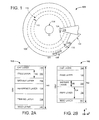
- FIG. 1 generally illustrates a top view block representation of an example data storage device 100 environment that can utilize a tuned magnetic element in accordance with various embodiments.
- the data storage device 100 is shown in a non-limiting configuration where an actuating assembly 102 is capable of positioning a transducing head 104 over a variety of locations on a magnetic storage media 106 where stored data bits 108 are located on predetermined data tracks 110 configured with a width 112 and corresponding areal density that determines the storage capacity of the media 106.
- Movement of the storage media 106 can be facilitated through attachment to one or more spindle motors 114 that rotate during use to produce an air bearing surface (ABS) on which a slider portion 116 of the actuating assembly 102 flies to position a head gimbal assembly (HGA) 118, which includes the transducing head 104, over a predetermined portion of the media 106.
- ABS air bearing surface
- HGA head gimbal assembly
- the transducing head 104 can be configured with one or more transducing elements, such as a magnetic writer, magnetically responsive reader, and magnetic shields, which operate to program and read data from the selected data tracks 110 of the storage media 106, respectively.
- controlled motion of the actuating assembly 102 correspond with alignment of the transducers with the data tracks 110 defined on the storage media surfaces to write, read, and rewrite data.
- the head 104 has to be responsive to smaller magnetic flux signatures with reliable accuracy, which can be problematic when the physical size of the head 104 components are reduced and especially when a material defect is present.
- stack is an unlimited term within this disclosure that can be one or more vertically and horizontally aligned layers, constructed of magnetic and non-magnetic material that are capable of magnetic reading and writing.
- the term “stack” will be understood to mean a component that is constructed to respond to external data bits to provide access to external data bits in any operational environment.
- a magnetic stack may be a data read or write configuration that can differentiate between a plurality of data bits.
- FIGS. 2A and 2B respectively show magnetic stacks 130 and 150 each capable of being used in the data storage device 100 of FIG. 1 .
- the magnetic stack 130 is constructed with a fixed magnetization pinning layer 134 contacting a fixed magnetization reference layer 136 opposite a non-magnetic barrier layer 138 from a magnetically free layer 140.
- the free layer 140 responds to an external data bit while the reference layer 136 maintains a fixed magnetization due to the exchange coupling with the pinning layer 134, an external data bit can be read as a logic state.
- seed 142 and cap 144 layers can be positioned on a single, or opposite sides of the stack 130 in various embodiments.
- Construction of the abutted junction magnetic stack 130 can have a shield-to-shield spacing 146 and free layer thickness 148 that determine the magnetic extent of the stack 130 and the possible data track resolution.
- the inclusion of the reference 136 and pinning 134 layers can correspond to a smaller free layer thickness 148, high resistance-area, and reduced magnetoresistive ratio between the free 140 and reference 136 layers.
- the trilayer stack 150 may be used to read data bits with a reduced shield-to-shield spacing 152 and thicker free layer thickness 154 compared to the abutted junction stack 130.
- the trilayer stack 150 has first 156 and second 158 magnetically free layers that are separated by a barrier layer 160 and set to default magnetizations by biasing structures external to the trilayer stack 150.
- the trilayer stack 150 may be smaller and have thicker free layers 156 and 158, the barrier layers 138 and 160 of the respective stacks 130 and 150 have presented difficulties in providing ample magnetoresistive ratios and resistance-areas capable of accurately sensing densely packed data bits.
- the effective barrier height or more specifically the electrostatic potential experienced by tunneling electrons, from the free layers 140 and 158 across the barrier layers 138 and 160 to the reference 136 and free 156 layers, or vice versa, respectively. That is, the single material composition and the consequent electronic band structure of the barrier layers 138 and 160 can determine the effective barrier height and consequently the resistance-area and tunnel magnetoresistive ratio of the stacks 130 and 150, regardless of the size of the free layers 148 and 154.
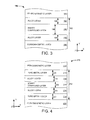
- FIG. 3 displays a portion of an example magnetic stack 180 tuned with a multilayer barrier structure 182 that can provide a predetermined resistance-area and magnetoresistive ratio by optimizing the effective barrier height in accordance with various embodiments.
- the multilayer barrier structure 182 can be utilized in a variety of non-limiting data sensing laminations, like the abutted junction and trilayer stacks of FIGS. 2A and 2B , ferromagnetic layers 184 and 186 bookend the barrier structure 182 to generally provide spatial context.
- the multilayer barrier structure 182 is constructed with a binary compound layer 188 disposed between and contacting first 190 and second 192 alloy layers.
- Various embodiments configure the binary compound as an alkaline earth metal combined with a different material to provide a predetermined lattice configuration, such as body centered cubic, and predetermined work function that determines the electrostatic barrier height seen by tunneling electrons.
- the binary compound layer comprises Magnesium Oxide, which can provide high signal-to-noise ratios and compatibility with detection electronics. While the use of MgO can provide structural and operational benefits over a pure non-magnetic barrier layer like Copper, placement of the alloy layers 190 and 192 each constructed of alloys of the metal material in the binary compound layer 188 on opposite sides of the binary compound layer 188 can aid in promoting the predetermined lattice configuration and work function to lower the effective barrier height between the ferromagnetic layers 184 and 186.
- the material composition of the alloy layers 190 and 192 can be chosen in some embodiments to match the metal material of the binary compound layer 188, such as Mg, and be combined with a second material having a lower work function than the metal materials. Based on the following equation 1 and the work function property of various elements, the alloy layers 190 and 192 can be tuned to lower the effective barrier height.
- ⁇ AB ⁇ A + 1.41 d A ⁇ 2 ⁇ ⁇ A - ⁇ B - .34 ⁇ A + ⁇ B - .68
- ⁇ A is the work function of the element with the smaller work function property
- ⁇ B is the element with the larger work function
- d A is covalent bond strength.
- equation 1 yields Barium, Lithium, and Strontium as prospects to be combined with the alkaline earth metal found in the binary compound layer 188 due to having a lower work function than Mg alone and ease of forming binary alloys.
- the three prospective elements can additionally provide a lower electronic band gap than MgO when formed as an oxide with a lower oxide barrier height and crystal structure, which could reduce the effective band gap of the binary compound layer 188.
- Boron can bond with each element instead of diffusing into the binary compound layer, which can provide a means to reduce ferromagnetic coupling across the barrier structure 182.
- various embodiments form the alloy layers 190 and 192 of the barrier structure 182 of MgBa, MgLi, or MgSr with respective thicknesses 194 and 196 that may or may not match the thickness 198 of the binary compound layer 188 to provide a predetermined resistance-area.
- the alloy layers 190 and 192 are not required to have matching material compositions as the first alloy layer 190 may be constructed of MgBa while the second alloy layer 192 is formed of MgSr. Such diverse tuning capabilities can allow for precise resistance-area and effective barrier height tuning catered to a wide variety of data storage environments.
- the placement and material composition of the alloy layers 190 and 192 on either side of the binary compound layer 188 may provide a reduced resistance-area, but can suffer from deflated magnetoresistive ratios as the alloy layers 190 and 192 may not take the predetermined texture and lattice structure due at least in part to the minimal thickness, such as .5-2 ⁇ , and the deposition means like radio frequency sputtering.
- FIG. 4 shows a portion of an example magnetic stack 210 with a multilayer barrier structure 212 that uses pure metal layers 214 as textured seed and cap elements to ensure the predetermined texture and lattice matching for the alloy layers 216 and binary compound layer 218.
- the addition of the pure metal layers 214 can be in the form of materials that are similar or dissimilar to the alkaline earth metal (i.e. Mg) uniformly used in the binary compound 218 and alloy 216 layers. However, some embodiments do uniformly use a metal, such as Cu, as the pure metal layer 214 and one part of the alloy 216 and binary compound 218 layers.
- each layer of the multilayer barrier structure 212 has substantially the same thickness, such as 2 ⁇ , while in other embodiments the pure metal 214 and alloy 216 layers have smaller thicknesses 220 and 224 than the thickness 226 of the binary compound layer 218.
- FIG. 5 provides just such a magnetic element fabrication routine 240 conducted in accordance with various embodiments.
- a lower electrode material may initially be deposited at step 242 and may include at least a ferromagnetic layer, such as a magnetic shield, and may further comprise a seed layer.
- Step 244 corresponds with the formation of a trilayer stack lamination where the top and bottom electrodes are ferromagnetic free layers and the stack has no fixed magnetizations, but instead external bias structures like a side shield or bias magnet distal an air bearing surface.
- step 246 forms the first ferromagnetic free layer atop the lower electrode.
- step 250 instead of step 246 to form a fixed reference structure, such as a pinned magnetization layer coupled to a ferromagnetic reference layer.
- step 254 deposits the first pure metal layer of a predetermined material, such as Mg, and with a predetermined thickness.
- a pure metal layer is to be positioned between the ferromagnetic layers and the alloy layers of the multilayer barrier structure.
- step 254 deposits the first pure metal layer of a predetermined material, such as Mg, and with a predetermined thickness.
- a choice to not include a pure metal layer in the magnetic element or at the conclusion of the deposition of the first pure metal layer advances routine 240 to step 256, which forms the multilayer barrier structure with alloy layers, such as MgX where X is Ba, Li, or Sr, contacting opposite sides of a binary compound layer, such as MgO.
- the alloy layers are formed of MgO that can either be deposited as MgO or formed via oxidation of an Mg layer that may or may not be deposited in the presence of oxygen.
- the product of either technique is a thin layer of MgO that can be tuned to a predetermined thickness and texture to allow the binary compound layer to be MgBa, MgLi, or MgSr and have a lattice configuration, crystal structure, and work function that corresponds with a predetermined resistance-area.
- step 258 deposits a second pure metal layer if the metal layer was chosen from decision 252. No matter whether the second pure metal layer was deposited or not, step 260 forms the top electrode material, such as a ferromagnetic free layer, cap layer, and magnetic shield, atop the multilayer barrier structure to complete the magnetic element.
- various embodiments can condition the multilayer barrier structure through modified temperature treatments. That is, the stack can be exposed to cryogenic temperatures, such as 50 K, and/or exposed to elevated in-situ thermal temperatures to cause the materials of the multilayer barrier structure to react and provide the predetermined resistance-area, work function, and effective barrier height.
- cryogenic temperatures such as 50 K
- in-situ thermal temperatures to cause the materials of the multilayer barrier structure to react and provide the predetermined resistance-area, work function, and effective barrier height.
- routine 240 Through the various steps and decisions of routine 240, a magnetic element can be created with an optimized barrier structure tuned with various materials and thicknesses.
- routine 240 is not limited to the steps and decisions provided in FIG. 5 as an unlimited variety of processes can be added to the routine 240 while any of the existing aspects can be modified and deleted, at will. For example, a decision could be included before step 260 to determine if a heat/cooling treatment is to be conducted on the multilayer barrier structure.
- a magnetic element can be created with a reduced effective barrier height and resistance-area.
- the judicious selection of alkaline earth metal combinations for both the alloy and binary compound layers allows for large magnetoresistive ratios to be achieved despite reduced physical size of the barrier.
- the lower work functions of the alloy and binary compound layers having the same root metal element may yield a more robust tunneling barrier without increasing effective barrier height.
- the embodiments have been directed to magnetic sensing, it will be appreciated that the claimed invention can readily be utilized in any number of other applications, including data storage device applications.
Landscapes
- Engineering & Computer Science (AREA)
- Physics & Mathematics (AREA)
- Manufacturing & Machinery (AREA)
- Power Engineering (AREA)
- Crystallography & Structural Chemistry (AREA)
- Chemical & Material Sciences (AREA)
- Computer Hardware Design (AREA)
- Nanotechnology (AREA)
- Condensed Matter Physics & Semiconductors (AREA)
- General Physics & Mathematics (AREA)
- Spectroscopy & Molecular Physics (AREA)
- Hall/Mr Elements (AREA)
- Magnetic Heads (AREA)
- Measuring Magnetic Variables (AREA)
- Mram Or Spin Memory Techniques (AREA)
Description
- Various embodiments are generally directed to a magnetic element capable of reading data bits in high areal density, reduced form factor data storage environ.
- In accordance with various embodiments, a magnetic data reader may generally be configured with at least a magnetic stack having a multilayer barrier structure disposed between first and second ferromagnetic layers. The multilayer barrier structure can have a binary compound layer disposed between first and second alloy layers with the binary compound having a metal element and a second element where at least one alloy layer has the metal element and a third element dissimilar from the second element.
- According to a first aspect of the present invention, there is provided an apparatus comprising a magnetic stack with a multilayer barrier structure disposed between first and second ferromagnetic layers, the multilayer barrier structure having a binary compound layer disposed between first and second alloy layers, the binary compound comprising a metal element and a second element, at least one alloy layer comprising the metal element and a third element dissimilar from the second element.
- Preferably, the metal element comprises Magnesium.
- Alternatively, the second element preferably comprises Oxygen.
- Alternatively, the second element preferably, comprises Barium.
- Alternatively, the second element preferably comprises Lithium.
- Alternatively, the second element preferably comprises Strontium.
- Preferably, the magnetic stack comprises a trilayer lamination having first and second magnetically free layers without a fixed reference magnetization.
- Preferably, the magnetic stack comprises an abutted junction lamination having a fixed magnetization reference structure opposite the multilayer barrier structure from a magnetically free layer.
- Preferably, each alloy layer is disposed between one of the first and second ferromagnetic layers and the binary compound layer.
- Preferably, the first and second alloy layers have the same material composition.
- Preferably, the binary compound layer and at least one alloy layer each have a common thickness.
- Preferably, the binary compound layer and at least one alloy layer each have dissimilar thicknesses.
- In this case, it is further preferable that the first and second alloy layers have dissimilar material compositions.
- According to another aspect of the present invention, there is provided a magnetic element comprising: a magnetic stack with a multilayer barrier structure disposed between first and second ferromagnetic layers and between first and second pure metal layers, the multilayer barrier structure having a binary compound layer disposed between first and second alloy layers, the binary compound comprising a metal element and a second element, each alloy layer comprising the metal element and a third element dissimilar from the second element.
- Preferably, each pure metal layer comprises the metal element of the binary compound.
- Preferably, the binary compound layer comprises MgO and each alloy layer comprises MgX where X is chosen from the group of: Ba, Sr, and Li.
- Preferably, the binary compound layer comprises MgX where X is chosen from the group of: Ba, Sr, and Li, each alloy layer is MgO, and each pure metal layer is Mg.
- According to a further aspect of the present invention, there is provided a method comprising: constructing a lower electrode portion of a magnetic stack with at least one ferromagnetic layer; forming a multilayer barrier structure atop the lower electrode portion, the multilayer barrier structure having a binary compound layer disposed between first and second alloy layers, the binary compound comprising a metal element and a second element, at least one alloy layer comprising the metal element and a third element dissimilar from the second element; and depositing a top electrode portion a magnet stack with at least one ferromagnetic layer atop the multilayer barrier structure.
- Preferably, the method further comprises cooling the magnetic stack to a cryogenic temperature prior to the depositing step.
- Preferably, the method further comprises heating the magnetic stack to an elevated temperature prior to the depositing step.
- Embodiments of the present invention will now be described by way of further example only and with reference to the accompanying drawings, in which:
-
FIG. 1 is a block representation of an exemplary portion of a data storage device configured and operated in accordance with some embodiments. -
FIGS. 2A and 2B respectively show magnetic stack portions of exemplary magnetic elements capable of being used in the data storage element ofFIG. 1 . -
FIG. 3 displays a portion of an exemplary magnetic stack constructed in accordance with various embodiments. -
FIG. 4 shows a portion of an exemplary magnetic stack constructed in accordance with some embodiments. -
FIG. 5 provides a flowchart of an exemplary magnetic element fabrication routine carried out in accordance with various embodiments. - As modern electronics have continually reduced in physical size while demanding more data storage capacity and data access speeds, the scalability of various data transducing components is stressed close to the brink of reliability. The increase in data bit density corresponding to tighter data tracks emphasizes the resistance-area product of a magnetic element to quickly and accurately sense data bits. The combination of reduced physical size and resistance-area product for a data reader may be dominated by minute material defects that render magnetoresistive ratio to unreliable. Hence, optimizing the resistance-area product for a reduced form factor data storage device is a continued industry interest.
- Accordingly, various embodiments may generally be directed to a magnetic stack having a multilayer barrier structure disposed between first and second ferromagnetic layers, with the multilayer barrier structure having a binary compound layer disposed between first and second alloy layers and the binary compound has a metal element and a second element while at least one alloy layer has the metal element and a third element dissimilar from the second element. The ability to tune and optimize the multilayer barrier structure with different compounds can reduce the effective barrier height for the magnetic stack and lower the resistance-area for a given barrier thickness. An optimized multilayer barrier structure can further lower overall barrier thickness to allow more robust barrier materials to be used to achieve a predetermined resistance-area value.
- While a tuned barrier structure can be implemented into an unlimited variety of data storage environments,
FIG. 1 generally illustrates a top view block representation of an exampledata storage device 100 environment that can utilize a tuned magnetic element in accordance with various embodiments. Thedata storage device 100 is shown in a non-limiting configuration where anactuating assembly 102 is capable of positioning a transducinghead 104 over a variety of locations on amagnetic storage media 106 where storeddata bits 108 are located on predetermined data tracks 110 configured with awidth 112 and corresponding areal density that determines the storage capacity of themedia 106. Movement of thestorage media 106 can be facilitated through attachment to one ormore spindle motors 114 that rotate during use to produce an air bearing surface (ABS) on which aslider portion 116 of theactuating assembly 102 flies to position a head gimbal assembly (HGA) 118, which includes the transducinghead 104, over a predetermined portion of themedia 106. - The transducing
head 104 can be configured with one or more transducing elements, such as a magnetic writer, magnetically responsive reader, and magnetic shields, which operate to program and read data from the selected data tracks 110 of thestorage media 106, respectively. In this way, controlled motion of the actuatingassembly 102 correspond with alignment of the transducers with the data tracks 110 defined on the storage media surfaces to write, read, and rewrite data. Asdata bits 108 become more densely positioned in data tracks 110 with smallerradial widths 112, thehead 104 has to be responsive to smaller magnetic flux signatures with reliable accuracy, which can be problematic when the physical size of thehead 104 components are reduced and especially when a material defect is present. - It should be noted that the term "stack" is an unlimited term within this disclosure that can be one or more vertically and horizontally aligned layers, constructed of magnetic and non-magnetic material that are capable of magnetic reading and writing. Throughout the present application, the term "stack" will be understood to mean a component that is constructed to respond to external data bits to provide access to external data bits in any operational environment. For example, but not in any way limiting, a magnetic stack may be a data read or write configuration that can differentiate between a plurality of data bits.
-
FIGS. 2A and 2B respectively showmagnetic stacks data storage device 100 ofFIG. 1 . As shown inFIG. 2A , Themagnetic stack 130 is constructed with a fixedmagnetization pinning layer 134 contacting a fixedmagnetization reference layer 136 opposite anon-magnetic barrier layer 138 from a magneticallyfree layer 140. As thefree layer 140 responds to an external data bit while thereference layer 136 maintains a fixed magnetization due to the exchange coupling with thepinning layer 134, an external data bit can be read as a logic state. While not providing a fixed or free magnetization,seed 142 andcap 144 layers can be positioned on a single, or opposite sides of thestack 130 in various embodiments. - Construction of the abutted junction
magnetic stack 130 can have a shield-to-shield spacing 146 andfree layer thickness 148 that determine the magnetic extent of thestack 130 and the possible data track resolution. However, the inclusion of thereference 136 and pinning 134 layers can correspond to a smallerfree layer thickness 148, high resistance-area, and reduced magnetoresistive ratio between the free 140 and reference 136 layers. With those issues in mind, thetrilayer stack 150 may be used to read data bits with a reduced shield-to-shield spacing 152 and thickerfree layer thickness 154 compared to theabutted junction stack 130. - In operation, the
trilayer stack 150 has first 156 and second 158 magnetically free layers that are separated by abarrier layer 160 and set to default magnetizations by biasing structures external to thetrilayer stack 150. The relocation of any fixed magnetization structures from thestack 150 to elsewhere allow for the reducedphysical size 152 compared to the fixed magnetization having abuttedjunction stack 130. Even though thetrilayer stack 150 may be smaller and have thickerfree layers barrier layers respective stacks - Part of the issue facing both
magnetic stacks free layers barrier layers reference 136 and free 156 layers, or vice versa, respectively. That is, the single material composition and the consequent electronic band structure of thebarrier layers stacks free layers -
FIG. 3 displays a portion of an examplemagnetic stack 180 tuned with a multilayer barrier structure 182 that can provide a predetermined resistance-area and magnetoresistive ratio by optimizing the effective barrier height in accordance with various embodiments. As the multilayer barrier structure 182 can be utilized in a variety of non-limiting data sensing laminations, like the abutted junction and trilayer stacks ofFIGS. 2A and 2B ,ferromagnetic layers - The multilayer barrier structure 182 is constructed with a
binary compound layer 188 disposed between and contacting first 190 and second 192 alloy layers. Various embodiments configure the binary compound as an alkaline earth metal combined with a different material to provide a predetermined lattice configuration, such as body centered cubic, and predetermined work function that determines the electrostatic barrier height seen by tunneling electrons. - In a first non-limiting embodiment, the binary compound layer comprises Magnesium Oxide, which can provide high signal-to-noise ratios and compatibility with detection electronics. While the use of MgO can provide structural and operational benefits over a pure non-magnetic barrier layer like Copper, placement of the alloy layers 190 and 192 each constructed of alloys of the metal material in the
binary compound layer 188 on opposite sides of thebinary compound layer 188 can aid in promoting the predetermined lattice configuration and work function to lower the effective barrier height between theferromagnetic layers - The material composition of the alloy layers 190 and 192 can be chosen in some embodiments to match the metal material of the
binary compound layer 188, such as Mg, and be combined with a second material having a lower work function than the metal materials. Based on the following equation 1 and the work function property of various elements, the alloy layers 190 and 192 can be tuned to lower the effective barrier height.
In the equation, ϕA is the work function of the element with the smaller work function property, ϕB is the element with the larger work function, and dA is covalent bond strength. While any elements can be used to form the alloy layers 190 and 192, equation 1 yields Barium, Lithium, and Strontium as prospects to be combined with the alkaline earth metal found in thebinary compound layer 188 due to having a lower work function than Mg alone and ease of forming binary alloys. - The three prospective elements can additionally provide a lower electronic band gap than MgO when formed as an oxide with a lower oxide barrier height and crystal structure, which could reduce the effective band gap of the
binary compound layer 188. Yet another aspect of each of the three elements is that Boron can bond with each element instead of diffusing into the binary compound layer, which can provide a means to reduce ferromagnetic coupling across the barrier structure 182. Thusly, various embodiments form the alloy layers 190 and 192 of the barrier structure 182 of MgBa, MgLi, or MgSr withrespective thicknesses thickness 198 of thebinary compound layer 188 to provide a predetermined resistance-area. - It should be noted that the alloy layers 190 and 192 are not required to have matching material compositions as the
first alloy layer 190 may be constructed of MgBa while thesecond alloy layer 192 is formed of MgSr. Such diverse tuning capabilities can allow for precise resistance-area and effective barrier height tuning catered to a wide variety of data storage environments. The placement and material composition of the alloy layers 190 and 192 on either side of thebinary compound layer 188 may provide a reduced resistance-area, but can suffer from deflated magnetoresistive ratios as the alloy layers 190 and 192 may not take the predetermined texture and lattice structure due at least in part to the minimal thickness, such as .5-2 Ǻ, and the deposition means like radio frequency sputtering. - Such concerns may spurn the addition of pure metal layers on opposite sides of the alloy layers 190 and 192.
FIG. 4 shows a portion of an examplemagnetic stack 210 with amultilayer barrier structure 212 that usespure metal layers 214 as textured seed and cap elements to ensure the predetermined texture and lattice matching for the alloy layers 216 andbinary compound layer 218. The addition of thepure metal layers 214 can be in the form of materials that are similar or dissimilar to the alkaline earth metal (i.e. Mg) uniformly used in thebinary compound 218 andalloy 216 layers. However, some embodiments do uniformly use a metal, such as Cu, as thepure metal layer 214 and one part of thealloy 216 andbinary compound 218 layers. - Regardless of the
pure metal layers 214thickness 220 and material, the position of thelayer 214 between theferromagnetic layers 222 and the alloy layers 216 places metallic material at the interface of thebarrier structure 212 and theferromagnetic layers 222 to provide reduced resistance-area and large magnetoresistive ratios. Themetal layer thickness 220 can be adjusted, along with the alloy layer thicknesses 224 and the binarycompound layer thickness 226, to provide a predetermined multilayer thickness between theferromagnetic layers 222. In some embodiments, each layer of themultilayer barrier structure 212 has substantially the same thickness, such as 2 Ǻ, while in other embodiments thepure metal 214 andalloy 216 layers havesmaller thicknesses thickness 226 of thebinary compound layer 218. - The ability to tune the various layers of the
multilayer barrier structure 212 for respective materials and thicknesses allows for catered optimization of the resistance-area of the electron tunnel junction. Such tuning can occur at any time and may adhere to a predetermined fabrication routine.FIG. 5 provides just such a magneticelement fabrication routine 240 conducted in accordance with various embodiments. While not required or limiting, a lower electrode material may initially be deposited atstep 242 and may include at least a ferromagnetic layer, such as a magnetic shield, and may further comprise a seed layer. - The formation of the lower electrode material(s) advances routine 240 to a choice of how the magnetic element is to be configured. Step 244 corresponds with the formation of a trilayer stack lamination where the top and bottom electrodes are ferromagnetic free layers and the stack has no fixed magnetizations, but instead external bias structures like a side shield or bias magnet distal an air bearing surface. In accordance, step 246 forms the first ferromagnetic free layer atop the lower electrode. Conversely, the choice to form an abutted junction stack in
step 248 proceeds to step 250 instead ofstep 246 to form a fixed reference structure, such as a pinned magnetization layer coupled to a ferromagnetic reference layer. - With the lower portion of the magnetic element constructed from
steps 242 and either step 246 or 250,decision 252 determines whether or not a pure metal layer is to be inserted. If a pure metal layer is to be positioned between the ferromagnetic layers and the alloy layers of the multilayer barrier structure, step 254 deposits the first pure metal layer of a predetermined material, such as Mg, and with a predetermined thickness. A choice to not include a pure metal layer in the magnetic element or at the conclusion of the deposition of the first pure metal layer advances routine 240 to step 256, which forms the multilayer barrier structure with alloy layers, such as MgX where X is Ba, Li, or Sr, contacting opposite sides of a binary compound layer, such as MgO. - Through various non-limiting embodiments, the alloy layers are formed of MgO that can either be deposited as MgO or formed via oxidation of an Mg layer that may or may not be deposited in the presence of oxygen. The product of either technique is a thin layer of MgO that can be tuned to a predetermined thickness and texture to allow the binary compound layer to be MgBa, MgLi, or MgSr and have a lattice configuration, crystal structure, and work function that corresponds with a predetermined resistance-area. Subsequent to the formation of the multilayer barrier structure in
step 256, step 258 deposits a second pure metal layer if the metal layer was chosen fromdecision 252. No matter whether the second pure metal layer was deposited or not, step 260 forms the top electrode material, such as a ferromagnetic free layer, cap layer, and magnetic shield, atop the multilayer barrier structure to complete the magnetic element. - Prior to the deposition of the top electrode material(s) in
step 260, various embodiments can condition the multilayer barrier structure through modified temperature treatments. That is, the stack can be exposed to cryogenic temperatures, such as 50 K, and/or exposed to elevated in-situ thermal temperatures to cause the materials of the multilayer barrier structure to react and provide the predetermined resistance-area, work function, and effective barrier height. - Through the various steps and decisions of routine 240, a magnetic element can be created with an optimized barrier structure tuned with various materials and thicknesses. However, routine 240 is not limited to the steps and decisions provided in
FIG. 5 as an unlimited variety of processes can be added to the routine 240 while any of the existing aspects can be modified and deleted, at will. For example, a decision could be included beforestep 260 to determine if a heat/cooling treatment is to be conducted on the multilayer barrier structure. - With the wide variety of magnetic stack features that can be tuned and optimized, a magnetic element can be created with a reduced effective barrier height and resistance-area. The judicious selection of alkaline earth metal combinations for both the alloy and binary compound layers allows for large magnetoresistive ratios to be achieved despite reduced physical size of the barrier. Moreover, the lower work functions of the alloy and binary compound layers having the same root metal element may yield a more robust tunneling barrier without increasing effective barrier height. In addition, while the embodiments have been directed to magnetic sensing, it will be appreciated that the claimed invention can readily be utilized in any number of other applications, including data storage device applications.
- It is to be understood that even though numerous characteristics and advantages of various embodiments of the present disclosure have been set forth in the foregoing description, together with details of the structure and function of various embodiments, this detailed description is illustrative only, and changes may be made in detail, especially in matters of structure and arrangements of parts within the principles of the present technology to the full extent indicated by the broad general meaning of the terms in which the appended claims are expressed. For example, the particular elements may vary depending on the particular application without departing from the scope of the present disclosure.
Claims (17)
- An apparatus comprising a magnetic stack with a multilayer barrier structure disposed between first and second ferromagnetic layers (184, 186), the multilayer barrier structure characterised by having a binary compound layer (188) disposed between first and second alloy layers (190, 192), the binary compound comprising a metal element and a second element, at least one alloy layer comprising the metal element and a third element dissimilar from the second element.
- The apparatus of claim 1, wherein the metal element comprises Magnesium.
- The apparatus of claim 1 or claim 2, wherein the second element comprises at least one of Oxygen, Barium, Lithium and Strontium.
- The apparatus of any one of the preceding claims, wherein the magnetic stack comprises a trilayer lamination having first and second magnetically free layers without a fixed reference magnetization.
- The apparatus of any one of claims 1 to 3, wherein the magnetic stack comprises an abutted junction lamination having a fixed magnetization reference structure opposite the multilayer barrier structure from a magnetically free layer.
- The apparatus of any one of the preceding claims, wherein each alloy layer is disposed between one of the first and second ferromagnetic layers and the binary compound layer.
- The apparatus of any one of the preceding claims, wherein the first and second alloy layers have the same material composition.
- The apparatus of any one of claims 1 to 6, wherein the first and second alloy layers have dissimilar material compositions.
- The apparatus of any one of the preceding claims, wherein the binary compound layer and at least one alloy layer each have a common thickness.
- The apparatus of any one of claims 1 to 8, wherein the binary compound layer and at least one alloy layer each have dissimilar thicknesses.
- The apparatus of any one of the preceding claims, wherein the magnetic stack is further disposed between first and second pure metal layers, and each alloy layer comprises the metal element and the third element dissimilar from the second element.
- The magnetic element of claim 11, wherein each pure metal layer comprises the metal element of the binary compound.
- The magnetic element of claim 11 or claim 12, wherein the binary compound layer comprises MgO and each alloy layer comprises MgX where X is chosen from the group of: Ba, Sr, and Li.
- The magnetic element of any one of claims 11 to 13, wherein the binary compound layer comprises MgX where X is chosen from the group of: Ba, Sr, and Li, each alloy layer is MgO, and each pure metal layer is Mg.
- A method comprising:constructing a lower electrode portion of a magnetic stack with at least one ferromagnetic layer (184);forming a multilayer barrier structure (182) atop the lower electrode portion, characterised in that the multilayer barrier structure having a binary compound layer (198) disposed between first and second alloy layers (190, 192), the binary compound comprising a metal element and a second element, at least one alloy layer comprising the metal element and a third element dissimilar from the second element; anddepositing a top electrode portion a magnet stack with at least one ferromagnetic layer (186) atop the multilayer barrier structure.
- The method of claim 15, further comprising cooling the magnetic stack to a cryogenic temperature prior to the depositing step.
- The method of claim 15 or claim 16, further comprising heating the magnetic stack to an elevated temperature prior to the depositing step.
Applications Claiming Priority (1)
| Application Number | Priority Date | Filing Date | Title |
|---|---|---|---|
| US13/690,532 US9034491B2 (en) | 2012-11-30 | 2012-11-30 | Low resistance area magnetic stack |
Publications (2)
| Publication Number | Publication Date |
|---|---|
| EP2738770A1 EP2738770A1 (en) | 2014-06-04 |
| EP2738770B1 true EP2738770B1 (en) | 2015-09-16 |
Family
ID=49667095
Family Applications (1)
| Application Number | Title | Priority Date | Filing Date |
|---|---|---|---|
| EP13195190.7A Not-in-force EP2738770B1 (en) | 2012-11-30 | 2013-11-29 | Low resistance area magnetic stack |
Country Status (5)
| Country | Link |
|---|---|
| US (1) | US9034491B2 (en) |
| EP (1) | EP2738770B1 (en) |
| JP (1) | JP5908882B2 (en) |
| KR (1) | KR101536629B1 (en) |
| CN (1) | CN103854673B (en) |
Families Citing this family (4)
| Publication number | Priority date | Publication date | Assignee | Title |
|---|---|---|---|---|
| US9218826B1 (en) * | 2013-08-16 | 2015-12-22 | Seagate Technology Llc | Tuned horizontally symmetric magnetic stack |
| TWI569484B (en) * | 2014-01-24 | 2017-02-01 | 國立臺灣大學 | Magnetic tunnel junction with superlattice barriers and device comprising a magnetic tunnel junction with superlattice barriers |
| DE102016100750A1 (en) * | 2016-01-18 | 2017-07-20 | Airbus Operations Gmbh | Vehicle body and method for mounting a vehicle body |
| US9856557B1 (en) | 2016-01-22 | 2018-01-02 | Seagate Technology Llc | Fabrication of a multi-layered magnetic element |
Family Cites Families (29)
| Publication number | Priority date | Publication date | Assignee | Title |
|---|---|---|---|---|
| JP3657916B2 (en) * | 2001-02-01 | 2005-06-08 | 株式会社東芝 | Magnetoresistive head and perpendicular magnetic recording / reproducing apparatus |
| US6847509B2 (en) * | 2001-02-01 | 2005-01-25 | Kabushiki Kaisha Toshiba | Magnetoresistive head and perpendicular magnetic recording-reproducing apparatus |
| US6347049B1 (en) * | 2001-07-25 | 2002-02-12 | International Business Machines Corporation | Low resistance magnetic tunnel junction device with bilayer or multilayer tunnel barrier |
| JP3749873B2 (en) * | 2002-03-28 | 2006-03-01 | 株式会社東芝 | Magnetoresistive element, magnetic head, and magnetic reproducing apparatus |
| US6849464B2 (en) * | 2002-06-10 | 2005-02-01 | Micron Technology, Inc. | Method of fabricating a multilayer dielectric tunnel barrier structure |
| US6743642B2 (en) * | 2002-11-06 | 2004-06-01 | International Business Machines Corporation | Bilayer CMP process to improve surface roughness of magnetic stack in MRAM technology |
| US7780820B2 (en) * | 2005-11-16 | 2010-08-24 | Headway Technologies, Inc. | Low resistance tunneling magnetoresistive sensor with natural oxidized double MgO barrier |
| SE531384C2 (en) * | 2006-02-10 | 2009-03-17 | Vnk Innovation Ab | Multiple magnetoresistance devices based on metal doped magnesium oxide |
| JP4496189B2 (en) * | 2006-09-28 | 2010-07-07 | 株式会社東芝 | Magnetoresistive element and magnetoresistive random access memory |
| JP4343941B2 (en) * | 2006-11-06 | 2009-10-14 | Tdk株式会社 | Magnetoresistive element, thin film magnetic head, head gimbal assembly, hard disk device, and method of manufacturing magnetoresistive element |
| JP4492604B2 (en) * | 2006-11-10 | 2010-06-30 | Tdk株式会社 | Magnetoresistive element, thin film magnetic head, head gimbal assembly, and hard disk drive |
| US7929257B2 (en) * | 2007-02-23 | 2011-04-19 | Tdk Corporation | Magnetic thin film having spacer layer that contains CuZn |
| US7888756B2 (en) * | 2007-03-22 | 2011-02-15 | Everspin Technologies, Inc. | MRAM tunnel barrier structure and methods |
| JP2008263031A (en) * | 2007-04-11 | 2008-10-30 | Toshiba Corp | Magnetoresistance effect element, its manufacturing method, magnetic memory device provided with magnetoresistance effect element and its manufacturing method |
| JP4996390B2 (en) * | 2007-08-28 | 2012-08-08 | 株式会社東芝 | Spin FET and magnetoresistance effect element |
| JP4703660B2 (en) * | 2008-01-11 | 2011-06-15 | 株式会社東芝 | Spin MOS field effect transistor |
| US8289663B2 (en) | 2008-04-25 | 2012-10-16 | Headway Technologies, Inc. | Ultra low RA (resistance x area) sensors having a multilayer non-magnetic spacer between pinned and free layers |
| WO2010026667A1 (en) * | 2008-09-03 | 2010-03-11 | Canon Anelva Corporation | Ferromagnetic preferred grain growth promotion seed layer for amorphous or microcrystalline mgo tunnel barrier |
| JP2010080839A (en) * | 2008-09-29 | 2010-04-08 | Toshiba Corp | Method of manufacturing magneto-resistance effect device, the magneto-resistance effect device, magnetic head assembly, and magnetic recording and reproducing apparatus |
| JP2010109319A (en) * | 2008-09-30 | 2010-05-13 | Canon Anelva Corp | Fabricating method of magnetoresistive element, and storage medium |
| US8031445B2 (en) * | 2008-10-08 | 2011-10-04 | Headway Technologies, Inc. | Low noise magneto-resistive sensor utilizing magnetic noise cancellation |
| CN102458852B (en) | 2009-06-02 | 2015-10-14 | 新加坡科技研究局 | multilayer barrier film |
| JP5502900B2 (en) * | 2009-12-28 | 2014-05-28 | キヤノンアネルバ株式会社 | Method for manufacturing magnetoresistive element |
| US8659855B2 (en) * | 2010-03-19 | 2014-02-25 | Seagate Technology Llc | Trilayer reader with current constraint at the ABS |
| US8202572B2 (en) | 2010-11-22 | 2012-06-19 | Headway Technologies, Inc. | TMR device with improved MgO barrier |
| US8427791B2 (en) | 2010-11-23 | 2013-04-23 | HGST Netherlands B.V. | Magnetic tunnel junction having a magnetic insertion layer and methods of producing the same |
| US8405935B2 (en) * | 2010-12-28 | 2013-03-26 | Tdk Corporation | Magneto-resistive effect element having spacer layer including main spacer layer containing gallium oxide and nonmagnetic layer |
| US8570691B2 (en) | 2011-04-07 | 2013-10-29 | HGST Netherlands B.V. | TMR sensor film using a tantalum insertion layer and systems thereof |
| US8987006B2 (en) | 2011-04-22 | 2015-03-24 | Samsung Electronics Co., Ltd. | Method and system for providing a magnetic junction having an engineered barrier layer |
-
2012
- 2012-11-30 US US13/690,532 patent/US9034491B2/en active Active
-
2013
- 2013-11-22 KR KR1020130143042A patent/KR101536629B1/en active IP Right Grant
- 2013-11-29 JP JP2013247176A patent/JP5908882B2/en active Active
- 2013-11-29 CN CN201310629462.5A patent/CN103854673B/en active Active
- 2013-11-29 EP EP13195190.7A patent/EP2738770B1/en not_active Not-in-force
Also Published As
| Publication number | Publication date |
|---|---|
| KR101536629B1 (en) | 2015-07-14 |
| CN103854673A (en) | 2014-06-11 |
| JP2014143398A (en) | 2014-08-07 |
| EP2738770A1 (en) | 2014-06-04 |
| CN103854673B (en) | 2017-06-30 |
| US20140154528A1 (en) | 2014-06-05 |
| JP5908882B2 (en) | 2016-04-26 |
| US9034491B2 (en) | 2015-05-19 |
Similar Documents
| Publication | Publication Date | Title |
|---|---|---|
| US8077435B1 (en) | Current perpendicular-to-plane read sensor with back shield | |
| US9632149B2 (en) | Magnetic layer with grain refining agent | |
| US8922950B2 (en) | Multi-layer magnetoresistive shield with transition metal layer | |
| US8373948B2 (en) | Tunnel magnetoresistance (TMR) structures with MGO barrier and methods of making same | |
| US9001474B2 (en) | Magnetic element with biasing structure distal the air bearing surface | |
| US9293159B2 (en) | Positive and negative magnetostriction ultrahigh linear density sensor | |
| US9165570B2 (en) | Data reader with magnetic seed lamination | |
| US9928857B2 (en) | Method of making a bottom shield stabilized magnetic seed layer | |
| CN105679336A (en) | Tunneling magnetoresistive (TMR) read head with reduced gap thickness | |
| US8842396B1 (en) | Magnetic sensor with differing stripe heights | |
| US8879214B2 (en) | Half metal trilayer TMR reader with negative interlayer coupling | |
| EP2738770B1 (en) | Low resistance area magnetic stack | |
| US9454978B2 (en) | Sensor structure having increased thermal stability | |
| US7773348B2 (en) | High coercivity hard magnetic seedlayer | |
| US8995096B2 (en) | Magnetic element side shield with diffusion barrier | |
| US9218826B1 (en) | Tuned horizontally symmetric magnetic stack | |
| US20160284989A1 (en) | Systems and methods for controlling soft bias thickness for tunnel magnetoresistance readers | |
| US8867175B1 (en) | Magnetic shield base lamination | |
| US20240347073A1 (en) | Produce Thinner DTS and Adjustable Capacitance for TDMR Heads |
Legal Events
| Date | Code | Title | Description |
|---|---|---|---|
| PUAI | Public reference made under article 153(3) epc to a published international application that has entered the european phase |
Free format text: ORIGINAL CODE: 0009012 |
|
| 17P | Request for examination filed |
Effective date: 20131219 |
|
| AK | Designated contracting states |
Kind code of ref document: A1 Designated state(s): AL AT BE BG CH CY CZ DE DK EE ES FI FR GB GR HR HU IE IS IT LI LT LU LV MC MK MT NL NO PL PT RO RS SE SI SK SM TR |
|
| AX | Request for extension of the european patent |
Extension state: BA ME |
|
| RBV | Designated contracting states (corrected) |
Designated state(s): AL AT BE BG CH CY CZ DE DK EE ES FI FR GB GR HR HU IE IS IT LI LT LU LV MC MK MT NL NO PL PT RO RS SE SI SK SM TR |
|
| GRAP | Despatch of communication of intention to grant a patent |
Free format text: ORIGINAL CODE: EPIDOSNIGR1 |
|
| RIC1 | Information provided on ipc code assigned before grant |
Ipc: H01L 27/22 20060101ALI20150317BHEP Ipc: H01L 43/12 20060101ALI20150317BHEP Ipc: G01R 33/09 20060101ALI20150317BHEP Ipc: G01R 33/00 20060101ALI20150317BHEP Ipc: H01F 10/32 20060101ALI20150317BHEP Ipc: G11B 5/31 20060101ALI20150317BHEP Ipc: H01L 43/08 20060101ALI20150317BHEP Ipc: G11C 11/16 20060101AFI20150317BHEP Ipc: G11B 5/39 20060101ALI20150317BHEP |
|
| INTG | Intention to grant announced |
Effective date: 20150401 |
|
| GRAS | Grant fee paid |
Free format text: ORIGINAL CODE: EPIDOSNIGR3 |
|
| GRAA | (expected) grant |
Free format text: ORIGINAL CODE: 0009210 |
|
| AK | Designated contracting states |
Kind code of ref document: B1 Designated state(s): AL AT BE BG CH CY CZ DE DK EE ES FI FR GB GR HR HU IE IS IT LI LT LU LV MC MK MT NL NO PL PT RO RS SE SI SK SM TR |
|
| REG | Reference to a national code |
Ref country code: GB Ref legal event code: FG4D |
|
| REG | Reference to a national code |
Ref country code: CH Ref legal event code: EP |
|
| REG | Reference to a national code |
Ref country code: IE Ref legal event code: FG4D |
|
| REG | Reference to a national code |
Ref country code: AT Ref legal event code: REF Ref document number: 750356 Country of ref document: AT Kind code of ref document: T Effective date: 20151015 |
|
| REG | Reference to a national code |
Ref country code: DE Ref legal event code: R096 Ref document number: 602013003098 Country of ref document: DE |
|
| REG | Reference to a national code |
Ref country code: NL Ref legal event code: MP Effective date: 20150916 |
|
| PG25 | Lapsed in a contracting state [announced via postgrant information from national office to epo] |
Ref country code: GR Free format text: LAPSE BECAUSE OF FAILURE TO SUBMIT A TRANSLATION OF THE DESCRIPTION OR TO PAY THE FEE WITHIN THE PRESCRIBED TIME-LIMIT Effective date: 20151217 Ref country code: NO Free format text: LAPSE BECAUSE OF FAILURE TO SUBMIT A TRANSLATION OF THE DESCRIPTION OR TO PAY THE FEE WITHIN THE PRESCRIBED TIME-LIMIT Effective date: 20151216 Ref country code: FI Free format text: LAPSE BECAUSE OF FAILURE TO SUBMIT A TRANSLATION OF THE DESCRIPTION OR TO PAY THE FEE WITHIN THE PRESCRIBED TIME-LIMIT Effective date: 20150916 Ref country code: LV Free format text: LAPSE BECAUSE OF FAILURE TO SUBMIT A TRANSLATION OF THE DESCRIPTION OR TO PAY THE FEE WITHIN THE PRESCRIBED TIME-LIMIT Effective date: 20150916 Ref country code: LT Free format text: LAPSE BECAUSE OF FAILURE TO SUBMIT A TRANSLATION OF THE DESCRIPTION OR TO PAY THE FEE WITHIN THE PRESCRIBED TIME-LIMIT Effective date: 20150916 |
|
| PGFP | Annual fee paid to national office [announced via postgrant information from national office to epo] |
Ref country code: DE Payment date: 20151125 Year of fee payment: 3 |
|
| REG | Reference to a national code |
Ref country code: LT Ref legal event code: MG4D |
|
| REG | Reference to a national code |
Ref country code: AT Ref legal event code: MK05 Ref document number: 750356 Country of ref document: AT Kind code of ref document: T Effective date: 20150916 |
|
| PG25 | Lapsed in a contracting state [announced via postgrant information from national office to epo] |
Ref country code: RS Free format text: LAPSE BECAUSE OF FAILURE TO SUBMIT A TRANSLATION OF THE DESCRIPTION OR TO PAY THE FEE WITHIN THE PRESCRIBED TIME-LIMIT Effective date: 20150916 Ref country code: SE Free format text: LAPSE BECAUSE OF FAILURE TO SUBMIT A TRANSLATION OF THE DESCRIPTION OR TO PAY THE FEE WITHIN THE PRESCRIBED TIME-LIMIT Effective date: 20150916 Ref country code: HR Free format text: LAPSE BECAUSE OF FAILURE TO SUBMIT A TRANSLATION OF THE DESCRIPTION OR TO PAY THE FEE WITHIN THE PRESCRIBED TIME-LIMIT Effective date: 20150916 |
|
| PG25 | Lapsed in a contracting state [announced via postgrant information from national office to epo] |
Ref country code: NL Free format text: LAPSE BECAUSE OF FAILURE TO SUBMIT A TRANSLATION OF THE DESCRIPTION OR TO PAY THE FEE WITHIN THE PRESCRIBED TIME-LIMIT Effective date: 20150916 |
|
| PG25 | Lapsed in a contracting state [announced via postgrant information from national office to epo] |
Ref country code: IS Free format text: LAPSE BECAUSE OF FAILURE TO SUBMIT A TRANSLATION OF THE DESCRIPTION OR TO PAY THE FEE WITHIN THE PRESCRIBED TIME-LIMIT Effective date: 20160116 Ref country code: CZ Free format text: LAPSE BECAUSE OF FAILURE TO SUBMIT A TRANSLATION OF THE DESCRIPTION OR TO PAY THE FEE WITHIN THE PRESCRIBED TIME-LIMIT Effective date: 20150916 Ref country code: SK Free format text: LAPSE BECAUSE OF FAILURE TO SUBMIT A TRANSLATION OF THE DESCRIPTION OR TO PAY THE FEE WITHIN THE PRESCRIBED TIME-LIMIT Effective date: 20150916 Ref country code: ES Free format text: LAPSE BECAUSE OF FAILURE TO SUBMIT A TRANSLATION OF THE DESCRIPTION OR TO PAY THE FEE WITHIN THE PRESCRIBED TIME-LIMIT Effective date: 20150916 Ref country code: IT Free format text: LAPSE BECAUSE OF FAILURE TO SUBMIT A TRANSLATION OF THE DESCRIPTION OR TO PAY THE FEE WITHIN THE PRESCRIBED TIME-LIMIT Effective date: 20150916 Ref country code: EE Free format text: LAPSE BECAUSE OF FAILURE TO SUBMIT A TRANSLATION OF THE DESCRIPTION OR TO PAY THE FEE WITHIN THE PRESCRIBED TIME-LIMIT Effective date: 20150916 |
|
| PG25 | Lapsed in a contracting state [announced via postgrant information from national office to epo] |
Ref country code: PT Free format text: LAPSE BECAUSE OF FAILURE TO SUBMIT A TRANSLATION OF THE DESCRIPTION OR TO PAY THE FEE WITHIN THE PRESCRIBED TIME-LIMIT Effective date: 20160118 Ref country code: RO Free format text: LAPSE BECAUSE OF FAILURE TO SUBMIT A TRANSLATION OF THE DESCRIPTION OR TO PAY THE FEE WITHIN THE PRESCRIBED TIME-LIMIT Effective date: 20150916 Ref country code: AT Free format text: LAPSE BECAUSE OF FAILURE TO SUBMIT A TRANSLATION OF THE DESCRIPTION OR TO PAY THE FEE WITHIN THE PRESCRIBED TIME-LIMIT Effective date: 20150916 Ref country code: PL Free format text: LAPSE BECAUSE OF FAILURE TO SUBMIT A TRANSLATION OF THE DESCRIPTION OR TO PAY THE FEE WITHIN THE PRESCRIBED TIME-LIMIT Effective date: 20150916 |
|
| REG | Reference to a national code |
Ref country code: DE Ref legal event code: R097 Ref document number: 602013003098 Country of ref document: DE |
|
| PG25 | Lapsed in a contracting state [announced via postgrant information from national office to epo] |
Ref country code: LU Free format text: LAPSE BECAUSE OF FAILURE TO SUBMIT A TRANSLATION OF THE DESCRIPTION OR TO PAY THE FEE WITHIN THE PRESCRIBED TIME-LIMIT Effective date: 20151129 Ref country code: MC Free format text: LAPSE BECAUSE OF FAILURE TO SUBMIT A TRANSLATION OF THE DESCRIPTION OR TO PAY THE FEE WITHIN THE PRESCRIBED TIME-LIMIT Effective date: 20150916 |
|
| PLBE | No opposition filed within time limit |
Free format text: ORIGINAL CODE: 0009261 |
|
| STAA | Information on the status of an ep patent application or granted ep patent |
Free format text: STATUS: NO OPPOSITION FILED WITHIN TIME LIMIT |
|
| 26N | No opposition filed |
Effective date: 20160617 |
|
| REG | Reference to a national code |
Ref country code: IE Ref legal event code: MM4A |
|
| REG | Reference to a national code |
Ref country code: FR Ref legal event code: ST Effective date: 20160729 |
|
| PG25 | Lapsed in a contracting state [announced via postgrant information from national office to epo] |
Ref country code: DK Free format text: LAPSE BECAUSE OF FAILURE TO SUBMIT A TRANSLATION OF THE DESCRIPTION OR TO PAY THE FEE WITHIN THE PRESCRIBED TIME-LIMIT Effective date: 20150916 |
|
| PG25 | Lapsed in a contracting state [announced via postgrant information from national office to epo] |
Ref country code: IE Free format text: LAPSE BECAUSE OF NON-PAYMENT OF DUE FEES Effective date: 20151129 |
|
| PG25 | Lapsed in a contracting state [announced via postgrant information from national office to epo] |
Ref country code: FR Free format text: LAPSE BECAUSE OF NON-PAYMENT OF DUE FEES Effective date: 20151130 Ref country code: SI Free format text: LAPSE BECAUSE OF FAILURE TO SUBMIT A TRANSLATION OF THE DESCRIPTION OR TO PAY THE FEE WITHIN THE PRESCRIBED TIME-LIMIT Effective date: 20150916 |
|
| PG25 | Lapsed in a contracting state [announced via postgrant information from national office to epo] |
Ref country code: BE Free format text: LAPSE BECAUSE OF FAILURE TO SUBMIT A TRANSLATION OF THE DESCRIPTION OR TO PAY THE FEE WITHIN THE PRESCRIBED TIME-LIMIT Effective date: 20150916 |
|
| PG25 | Lapsed in a contracting state [announced via postgrant information from national office to epo] |
Ref country code: BG Free format text: LAPSE BECAUSE OF FAILURE TO SUBMIT A TRANSLATION OF THE DESCRIPTION OR TO PAY THE FEE WITHIN THE PRESCRIBED TIME-LIMIT Effective date: 20150916 Ref country code: HU Free format text: LAPSE BECAUSE OF FAILURE TO SUBMIT A TRANSLATION OF THE DESCRIPTION OR TO PAY THE FEE WITHIN THE PRESCRIBED TIME-LIMIT; INVALID AB INITIO Effective date: 20131129 |
|
| REG | Reference to a national code |
Ref country code: DE Ref legal event code: R119 Ref document number: 602013003098 Country of ref document: DE |
|
| PG25 | Lapsed in a contracting state [announced via postgrant information from national office to epo] |
Ref country code: CY Free format text: LAPSE BECAUSE OF FAILURE TO SUBMIT A TRANSLATION OF THE DESCRIPTION OR TO PAY THE FEE WITHIN THE PRESCRIBED TIME-LIMIT Effective date: 20150916 |
|
| REG | Reference to a national code |
Ref country code: CH Ref legal event code: PL |
|
| PG25 | Lapsed in a contracting state [announced via postgrant information from national office to epo] |
Ref country code: CH Free format text: LAPSE BECAUSE OF NON-PAYMENT OF DUE FEES Effective date: 20161130 Ref country code: LI Free format text: LAPSE BECAUSE OF NON-PAYMENT OF DUE FEES Effective date: 20161130 |
|
| PG25 | Lapsed in a contracting state [announced via postgrant information from national office to epo] |
Ref country code: MT Free format text: LAPSE BECAUSE OF FAILURE TO SUBMIT A TRANSLATION OF THE DESCRIPTION OR TO PAY THE FEE WITHIN THE PRESCRIBED TIME-LIMIT Effective date: 20150916 |
|
| PG25 | Lapsed in a contracting state [announced via postgrant information from national office to epo] |
Ref country code: DE Free format text: LAPSE BECAUSE OF NON-PAYMENT OF DUE FEES Effective date: 20170601 |
|
| PG25 | Lapsed in a contracting state [announced via postgrant information from national office to epo] |
Ref country code: SM Free format text: LAPSE BECAUSE OF FAILURE TO SUBMIT A TRANSLATION OF THE DESCRIPTION OR TO PAY THE FEE WITHIN THE PRESCRIBED TIME-LIMIT Effective date: 20150916 |
|
| PG25 | Lapsed in a contracting state [announced via postgrant information from national office to epo] |
Ref country code: MK Free format text: LAPSE BECAUSE OF FAILURE TO SUBMIT A TRANSLATION OF THE DESCRIPTION OR TO PAY THE FEE WITHIN THE PRESCRIBED TIME-LIMIT Effective date: 20150916 |
|
| GBPC | Gb: european patent ceased through non-payment of renewal fee |
Effective date: 20171129 |
|
| PG25 | Lapsed in a contracting state [announced via postgrant information from national office to epo] |
Ref country code: TR Free format text: LAPSE BECAUSE OF FAILURE TO SUBMIT A TRANSLATION OF THE DESCRIPTION OR TO PAY THE FEE WITHIN THE PRESCRIBED TIME-LIMIT Effective date: 20150916 Ref country code: AL Free format text: LAPSE BECAUSE OF FAILURE TO SUBMIT A TRANSLATION OF THE DESCRIPTION OR TO PAY THE FEE WITHIN THE PRESCRIBED TIME-LIMIT Effective date: 20150916 |
|
| PG25 | Lapsed in a contracting state [announced via postgrant information from national office to epo] |
Ref country code: GB Free format text: LAPSE BECAUSE OF NON-PAYMENT OF DUE FEES Effective date: 20171129 |