EP2738769A1 - Magnetoresistive element having enhanced exchange bias and thermal stability for spintronic devices - Google Patents
Magnetoresistive element having enhanced exchange bias and thermal stability for spintronic devices Download PDFInfo
- Publication number
- EP2738769A1 EP2738769A1 EP12290416.2A EP12290416A EP2738769A1 EP 2738769 A1 EP2738769 A1 EP 2738769A1 EP 12290416 A EP12290416 A EP 12290416A EP 2738769 A1 EP2738769 A1 EP 2738769A1
- Authority
- EP
- European Patent Office
- Prior art keywords
- layer
- magnetic
- magnetoresistive element
- antiferromagnetic
- magnetization
- Prior art date
- Legal status (The legal status is an assumption and is not a legal conclusion. Google has not performed a legal analysis and makes no representation as to the accuracy of the status listed.)
- Granted
Links
Images
Classifications
-
- H—ELECTRICITY
- H10—SEMICONDUCTOR DEVICES; ELECTRIC SOLID-STATE DEVICES NOT OTHERWISE PROVIDED FOR
- H10N—ELECTRIC SOLID-STATE DEVICES NOT OTHERWISE PROVIDED FOR
- H10N50/00—Galvanomagnetic devices
- H10N50/10—Magnetoresistive devices
-
- G—PHYSICS
- G11—INFORMATION STORAGE
- G11C—STATIC STORES
- G11C11/00—Digital stores characterised by the use of particular electric or magnetic storage elements; Storage elements therefor
- G11C11/02—Digital stores characterised by the use of particular electric or magnetic storage elements; Storage elements therefor using magnetic elements
- G11C11/16—Digital stores characterised by the use of particular electric or magnetic storage elements; Storage elements therefor using magnetic elements using elements in which the storage effect is based on magnetic spin effect
- G11C11/161—Digital stores characterised by the use of particular electric or magnetic storage elements; Storage elements therefor using magnetic elements using elements in which the storage effect is based on magnetic spin effect details concerning the memory cell structure, e.g. the layers of the ferromagnetic memory cell
-
- H—ELECTRICITY
- H01—ELECTRIC ELEMENTS
- H01F—MAGNETS; INDUCTANCES; TRANSFORMERS; SELECTION OF MATERIALS FOR THEIR MAGNETIC PROPERTIES
- H01F10/00—Thin magnetic films, e.g. of one-domain structure
- H01F10/32—Spin-exchange-coupled multilayers, e.g. nanostructured superlattices
- H01F10/324—Exchange coupling of magnetic film pairs via a very thin non-magnetic spacer, e.g. by exchange with conduction electrons of the spacer
- H01F10/3254—Exchange coupling of magnetic film pairs via a very thin non-magnetic spacer, e.g. by exchange with conduction electrons of the spacer the spacer being semiconducting or insulating, e.g. for spin tunnel junction [STJ]
-
- H—ELECTRICITY
- H01—ELECTRIC ELEMENTS
- H01F—MAGNETS; INDUCTANCES; TRANSFORMERS; SELECTION OF MATERIALS FOR THEIR MAGNETIC PROPERTIES
- H01F41/00—Apparatus or processes specially adapted for manufacturing or assembling magnets, inductances or transformers; Apparatus or processes specially adapted for manufacturing materials characterised by their magnetic properties
- H01F41/14—Apparatus or processes specially adapted for manufacturing or assembling magnets, inductances or transformers; Apparatus or processes specially adapted for manufacturing materials characterised by their magnetic properties for applying magnetic films to substrates
- H01F41/30—Apparatus or processes specially adapted for manufacturing or assembling magnets, inductances or transformers; Apparatus or processes specially adapted for manufacturing materials characterised by their magnetic properties for applying magnetic films to substrates for applying nanostructures, e.g. by molecular beam epitaxy [MBE]
- H01F41/302—Apparatus or processes specially adapted for manufacturing or assembling magnets, inductances or transformers; Apparatus or processes specially adapted for manufacturing materials characterised by their magnetic properties for applying magnetic films to substrates for applying nanostructures, e.g. by molecular beam epitaxy [MBE] for applying spin-exchange-coupled multilayers, e.g. nanostructured superlattices
- H01F41/303—Apparatus or processes specially adapted for manufacturing or assembling magnets, inductances or transformers; Apparatus or processes specially adapted for manufacturing materials characterised by their magnetic properties for applying magnetic films to substrates for applying nanostructures, e.g. by molecular beam epitaxy [MBE] for applying spin-exchange-coupled multilayers, e.g. nanostructured superlattices with exchange coupling adjustment of magnetic film pairs, e.g. interface modifications by reduction, oxidation
-
- H—ELECTRICITY
- H10—SEMICONDUCTOR DEVICES; ELECTRIC SOLID-STATE DEVICES NOT OTHERWISE PROVIDED FOR
- H10N—ELECTRIC SOLID-STATE DEVICES NOT OTHERWISE PROVIDED FOR
- H10N50/00—Galvanomagnetic devices
- H10N50/80—Constructional details
Definitions
- the present invention concerns a magnetoresistive element comprising a magnetic tunnel junction, the magnetoresistive element having enhanced exchange bias and enhanced stability to temperature cycles and improved life-time.
- Spintronic devices such as MRAM cells and devices based on MRAM cells, spin transfer torque oscillators or magnetic logic units, usually comprise a magnetic tunnel junction including a reference or sense layer, a tunnel barrier layer and a storage layer exchange-coupled or not with an antiferromagnetic layer.
- the antiferromagnetic layer is arranged to pin a magnetization of the ferromagnetic layer below a critical temperature of the antiferromagnetic layer and to free it above the critical temperature threshold.
- the exchange-coupling is occurring via a so-called exchange bias appearing when the antiferromagnetic layer is in contact with the ferromagnetic layer. The exchange bias is thus of great importance in the functioning of the spintronic devices.
- the exchange bias phenomenon is characterized by a shifted magnetization hysteresis loop measured for pinned ferromagnetic layer, as a function of an applied magnetic field.
- the exchange bias can be affected by the oxidation of the antiferromagnetic layer cause by the inevitable presence of residual oxygen atoms in the deposition chamber and introduced in the antiferromagnetic layer during the deposition process of the antiferromagnetic layer.
- diffusion of Mn atoms from the Mn containing antiferromagnetic layer into the adjacent ferromagnetic layer during annealing operations may result in a further reduction of the exchange bias and increases the coercivity of the storage layer. More generally, the manganese migration leads to a decrease of the magnetoresistance and an increase of the surface resistance in magnetic tunnel junctions.
- the present disclosure concerns a magnetoresistive element comprising a first magnetic layer having a first magnetization; a second magnetic layer having a second magnetization; a tunnel barrier layer comprised between the first and the second magnetic layers; and an antiferromagnetic layer exchanged coupling the second magnetic layer such that the second magnetization can be freely varied when the antiferromagnetic layer is heated above a critical temperature; the magnetic element further comprising an oxygen gettering layer between the second magnetic layer and the antiferromagnetic layer, or within the second magnetic layer.
- the magnetoresistive element disclosed herein has reduced insertion of oxygen atoms in the antiferromagnetic layer and/or reduced diffusion of manganese in the second magnetic layer resulting in an enhanced exchange bias and enhanced resistance to temperature cycles and improved life-time.
- a magnetoresistive element 1 comprises a magnetic tunnel junction comprising a first magnetic layer 21 having a first magnetization 210; a second magnetic layer 23 having a second magnetization 230; a tunnel barrier layer 22 comprised between the first and the second magnetic layers 21, 23; and an antiferromagnetic layer 24 exchanged coupling the second magnetic layer 23 such that the second magnetization 230 is pinned below a critical temperature of the antiferromagnetic layer 24 and can be freely varied when the antiferromagnetic layer 24 is heated at or above that critical temperature.
- the first and second magnetic layer 23 can comprise one or more of a CoFe, CoFeB or NiFe layer, or more generally a Co, Ni or Fe - based alloy.
- the antiferromagnetic layer 24 can comprise a manganese-based alloy, such as IrMn, PtMn or FeMn, a multilayer structure comprising a combination of manganese-based alloys, or any other suitable materials.
- the magnetoresistive element 1 further comprises an intermediate layer 25 arranged such as to act as an oxygen getter and/or prevent manganese migration within the magnetic tunnel junction stack.
- the intermediate layer 25 is comprised between the second magnetic 23 and the antiferromagnetic material 24, or within the second magnetic layer 23.
- the intermediate layer 25, or oxygen gettering layer can comprise a metallic element such as magnesium, aluminum, tantalum, niobium, chromium, titanium, vanadium.
- the intermediate layer 25 can comprise any material that has better oxygen gettering properties than the antiferromagnetic layer 24 and/or the second magnetic layer 23.
- the intermediate layer 25 comprises a material, such as magnesium, that is also able to block diffusion of manganese from the antiferromagnetic layer 24 into the second magnetic layer 23. Inhibiting diffusion of manganese from the antiferromagnetic layer 24 into the second magnetic layer 23 results in an enhanced exchange bias between the antiferromagnetic layer 24 and the second magnetic layer 23. The inhibited diffusion of manganese further allows the magnetoresistive element 1 to be higher temperature cycles without being degraded. The absence of manganese in the second magnetic layer 23 also diminishes possible galvanic corrosion of the second magnetic layer 23 due to the presence of the more noble manganese. Thus, the magnetoresistive element 1 should have enhanced resistance to temperature cycles and improved life-time.
- a material such as magnesium
- the intermediate layer 25 should be thin enough such as to conserve a significant magnetic exchange coupling between the antiferromagnetic layer 24 and the second magnetic layer 23.
- the thickness of the intermediate layer 25 is comprised between 0.1 nm and 3.0 nm and preferably the thickness of the intermediate layer 25 is about 0.2 nm.
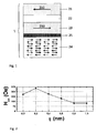
- Fig.2 reports the variation of the exchange bias field H ex as a function of the thickness t of the intermediate layer 25.
- the magnetoresistive element 1 comprises a stack comprising Ta 5 /Cu 3 / FeMn 12 / Mg t / NiFe 1.5 / CoFe 1 / MgO 1.4 / Ta 5, wherein the stack was annealed at 300°C for 90 min under a magnetic field of 1T (in this particular stack the antiferromagnetic layer 24 is represented by the FeMn layer, the intermediate lamination 25 by the Mg layer and the storage layer 23 by the bilayer NiFe 1.5 / CoFe 1.
- the tunnel barrier 22 is represented by the MgO layer).
- the intermediate layer 25 is made from magnesium.
- Fig. 2 shows a maximum in the exchange bias field H ex for a thickness of 0.2 nm of the intermediate layer 25 and that the exchange bias field H ex diminishes when the intermediate layer 25 is thicker than about 0.4 nm.
- the magnetoresistive element 1 disclosed herein can be included in a MRAM cell, for example, further comprising possibly one or more current lines (not shown) used for addressing the magnetic tunnel junction of MRAM cell, and possibly a selection transistor (also not shown). More generally, the magnetoresistive element 1 comprising the intermediate layer 25 can be advantageously employed in all type of spintronic devices including MRAM cells and devices based on MRAM cells, spin transfer torque oscillators or magnetic logic units.
- a magnetic memory device (not represented) can comprise, for example, a plurality of the MRAM cell comprising the magnetoresistive element 1 and arranged in rows and columns.
- the magnetic memory device can further comprise one or a plurality of current lines that connect the MRAM cells along a row and/or column.
Landscapes
- Engineering & Computer Science (AREA)
- Chemical & Material Sciences (AREA)
- Crystallography & Structural Chemistry (AREA)
- Power Engineering (AREA)
- Nanotechnology (AREA)
- Physics & Mathematics (AREA)
- Spectroscopy & Molecular Physics (AREA)
- Manufacturing & Machinery (AREA)
- Computer Hardware Design (AREA)
- Hall/Mr Elements (AREA)
- Mram Or Spin Memory Techniques (AREA)
Abstract
Description
- The present invention concerns a magnetoresistive element comprising a magnetic tunnel junction, the magnetoresistive element having enhanced exchange bias and enhanced stability to temperature cycles and improved life-time.
- Spintronic devices such as MRAM cells and devices based on MRAM cells, spin transfer torque oscillators or magnetic logic units, usually comprise a magnetic tunnel junction including a reference or sense layer, a tunnel barrier layer and a storage layer exchange-coupled or not with an antiferromagnetic layer. The antiferromagnetic layer is arranged to pin a magnetization of the ferromagnetic layer below a critical temperature of the antiferromagnetic layer and to free it above the critical temperature threshold. The exchange-coupling is occurring via a so-called exchange bias appearing when the antiferromagnetic layer is in contact with the ferromagnetic layer. The exchange bias is thus of great importance in the functioning of the spintronic devices.
- The exchange bias phenomenon is characterized by a shifted magnetization hysteresis loop measured for pinned ferromagnetic layer, as a function of an applied magnetic field. The exchange bias can be affected by the oxidation of the antiferromagnetic layer cause by the inevitable presence of residual oxygen atoms in the deposition chamber and introduced in the antiferromagnetic layer during the deposition process of the antiferromagnetic layer. Moreover, diffusion of Mn atoms from the Mn containing antiferromagnetic layer into the adjacent ferromagnetic layer during annealing operations may result in a further reduction of the exchange bias and increases the coercivity of the storage layer. More generally, the manganese migration leads to a decrease of the magnetoresistance and an increase of the surface resistance in magnetic tunnel junctions.
- The present disclosure concerns a magnetoresistive element comprising a first magnetic layer having a first magnetization; a second magnetic layer having a second magnetization; a tunnel barrier layer comprised between the first and the second magnetic layers; and an antiferromagnetic layer exchanged coupling the second magnetic layer such that the second magnetization can be freely varied when the antiferromagnetic layer is heated above a critical temperature; the magnetic element further comprising an oxygen gettering layer between the second magnetic layer and the antiferromagnetic layer, or within the second magnetic layer.
- The magnetoresistive element disclosed herein has reduced insertion of oxygen atoms in the antiferromagnetic layer and/or reduced diffusion of manganese in the second magnetic layer resulting in an enhanced exchange bias and enhanced resistance to temperature cycles and improved life-time.
- The invention will be better understood with the aid of the description of an embodiment given by way of example and illustrated by the figures, in which:
-
Fig. 1 is a schematic representation of a magnetoresistive element comprising an intermediate layer, according to an embodiment; and -
Fig. 2 reports the variation of the exchange bias field as a function of the thickness of the intermediate layer. - In an embodiment represented in
Fig. 1 , amagnetoresistive element 1 comprises a magnetic tunnel junction comprising a firstmagnetic layer 21 having a first magnetization 210; a secondmagnetic layer 23 having asecond magnetization 230; atunnel barrier layer 22 comprised between the first and the secondmagnetic layers antiferromagnetic layer 24 exchanged coupling the secondmagnetic layer 23 such that thesecond magnetization 230 is pinned below a critical temperature of theantiferromagnetic layer 24 and can be freely varied when theantiferromagnetic layer 24 is heated at or above that critical temperature. The first and secondmagnetic layer 23 can comprise one or more of a CoFe, CoFeB or NiFe layer, or more generally a Co, Ni or Fe - based alloy. Theantiferromagnetic layer 24 can comprise a manganese-based alloy, such as IrMn, PtMn or FeMn, a multilayer structure comprising a combination of manganese-based alloys, or any other suitable materials. - The
magnetoresistive element 1 further comprises anintermediate layer 25 arranged such as to act as an oxygen getter and/or prevent manganese migration within the magnetic tunnel junction stack. Theintermediate layer 25 is comprised between the second magnetic 23 and theantiferromagnetic material 24, or within the secondmagnetic layer 23. - To this end, the
intermediate layer 25, or oxygen gettering layer, can comprise a metallic element such as magnesium, aluminum, tantalum, niobium, chromium, titanium, vanadium. In fact, theintermediate layer 25 can comprise any material that has better oxygen gettering properties than theantiferromagnetic layer 24 and/or the secondmagnetic layer 23. - In a preferred embodiment, the
intermediate layer 25 comprises a material, such as magnesium, that is also able to block diffusion of manganese from theantiferromagnetic layer 24 into the secondmagnetic layer 23. Inhibiting diffusion of manganese from theantiferromagnetic layer 24 into the secondmagnetic layer 23 results in an enhanced exchange bias between theantiferromagnetic layer 24 and the secondmagnetic layer 23. The inhibited diffusion of manganese further allows themagnetoresistive element 1 to be higher temperature cycles without being degraded. The absence of manganese in the secondmagnetic layer 23 also diminishes possible galvanic corrosion of the secondmagnetic layer 23 due to the presence of the more noble manganese. Thus, themagnetoresistive element 1 should have enhanced resistance to temperature cycles and improved life-time. - The
intermediate layer 25 should be thin enough such as to conserve a significant magnetic exchange coupling between theantiferromagnetic layer 24 and the secondmagnetic layer 23. In an embodiment, the thickness of theintermediate layer 25 is comprised between 0.1 nm and 3.0 nm and preferably the thickness of theintermediate layer 25 is about 0.2 nm. -
Fig.2 reports the variation of the exchange bias field Hex as a function of the thickness t of theintermediate layer 25. In the example ofFig. 2 , themagnetoresistive element 1 comprises a stack comprising Ta 5 /Cu 3 / FeMn 12 / Mg t / NiFe 1.5 /CoFe 1 / MgO 1.4 / Ta 5, wherein the stack was annealed at 300°C for 90 min under a magnetic field of 1T (in this particular stack theantiferromagnetic layer 24 is represented by the FeMn layer, theintermediate lamination 25 by the Mg layer and thestorage layer 23 by the bilayer NiFe 1.5 /CoFe 1. Thetunnel barrier 22 is represented by the MgO layer). Theintermediate layer 25 is made from magnesium.Fig. 2 shows a maximum in the exchange bias field Hex for a thickness of 0.2 nm of theintermediate layer 25 and that the exchange bias field Hex diminishes when theintermediate layer 25 is thicker than about 0.4 nm. - The
magnetoresistive element 1 disclosed herein can be included in a MRAM cell, for example, further comprising possibly one or more current lines (not shown) used for addressing the magnetic tunnel junction of MRAM cell, and possibly a selection transistor (also not shown). More generally, themagnetoresistive element 1 comprising theintermediate layer 25 can be advantageously employed in all type of spintronic devices including MRAM cells and devices based on MRAM cells, spin transfer torque oscillators or magnetic logic units. - A magnetic memory device (not represented) can comprise, for example, a plurality of the MRAM cell comprising the
magnetoresistive element 1 and arranged in rows and columns. The magnetic memory device can further comprise one or a plurality of current lines that connect the MRAM cells along a row and/or column. -
- 1
- magnetoresistive element
- 21
- first magnetic layer
- 210
- first magnetization
- 23
- second magnetic layer
- 230
- second magnetization
- 24
- antiferromagnetic layer
- 25
- intermediate layer
- Hex
- exchange bias field
- t
- thickness
Claims (10)
- Magnetoresistive element (1) comprising a first magnetic layer (21) having a first magnetization (210); a second magnetic layer (23) having a second magnetization (230); a tunnel barrier layer (22) comprised between the first and the second magnetic layers (21, 23); and an antiferromagnetic layer (24) exchanged coupling the second magnetic layer (23) such that the second magnetization (230) is pinned below a critical temperature of the antiferromagnetic layer (24), and can be freely varied when the antiferromagnetic layer (24) is heated above the critical temperature; characterized in that
the magnetic element (1) further comprises an oxygen gettering layer (25) arranged such as to act as an oxygen getter and/or prevent manganese migration within the magnetic tunnel junction stack. - Magnetoresistive element (1) according to claim 1; wherein said oxygen gettering layer (25) is comprised between the second magnetic layer (23) and the antiferromagnetic layer (24),
- Magnetoresistive element (1) according to claim 1 or 2; wherein
said oxygen gettering layer (25) is comprised within the second magnetic layer (23). - Magnetoresistive element (1) according to any one of claims 1 to 3; wherein
said oxygen gettering layer (25) comprises one of magnesium, aluminum, tantalum, niobium, chromium, titanium, vanadium. - Magnetoresistive element (1) according to any one of claims 1 to 4; wherein
said oxygen gettering layer (25) comprises a material which is immiscible with manganese. - Magnetoresistive element (1) according to claim 5; wherein said oxygen gettering layer (25) comprises magnesium.
- Magnetoresistive element (1) according to any one of claims 1 to 6; wherein
said oxygen gettering layer (25) has a thickness comprised between 0.1 nm and 3.0 nm. - Magnetoresistive element (1) according to any one of claims 1 to 6; wherein
said oxygen gettering layer (25) has a thickness of about 0.2 nm. - MRAM cell comprising the magnetoresistive element (1) characterized by any one of claims 1 to 8.
- Magnetic memory device comprising a plurality of the MRAM cell according to claim 9.
Priority Applications (3)
| Application Number | Priority Date | Filing Date | Title |
|---|---|---|---|
| EP12290416.2A EP2738769B1 (en) | 2012-11-28 | 2012-11-28 | Magnetoresistive element having enhanced exchange bias and thermal stability for spintronic devices |
| PCT/EP2013/074191 WO2014082896A1 (en) | 2012-11-28 | 2013-11-19 | Magnetoresistive element having enhanced exchange bias and thermal stability for spintronic devices |
| US14/647,632 US9431601B2 (en) | 2012-11-28 | 2013-11-19 | Magnetoresistive element with oxygen getting layer having enhanced exchange bias and thermal stability for spintronic devices |
Applications Claiming Priority (1)
| Application Number | Priority Date | Filing Date | Title |
|---|---|---|---|
| EP12290416.2A EP2738769B1 (en) | 2012-11-28 | 2012-11-28 | Magnetoresistive element having enhanced exchange bias and thermal stability for spintronic devices |
Publications (2)
| Publication Number | Publication Date |
|---|---|
| EP2738769A1 true EP2738769A1 (en) | 2014-06-04 |
| EP2738769B1 EP2738769B1 (en) | 2019-09-04 |
Family
ID=47435832
Family Applications (1)
| Application Number | Title | Priority Date | Filing Date |
|---|---|---|---|
| EP12290416.2A Active EP2738769B1 (en) | 2012-11-28 | 2012-11-28 | Magnetoresistive element having enhanced exchange bias and thermal stability for spintronic devices |
Country Status (3)
| Country | Link |
|---|---|
| US (1) | US9431601B2 (en) |
| EP (1) | EP2738769B1 (en) |
| WO (1) | WO2014082896A1 (en) |
Cited By (2)
| Publication number | Priority date | Publication date | Assignee | Title |
|---|---|---|---|---|
| CN106463169A (en) * | 2014-06-17 | 2017-02-22 | 克罗科斯科技公司 | Self-referenced multibit MRAM cell having a synthetic antiferromagnetic storage layer |
| CN108292700A (en) * | 2015-12-07 | 2018-07-17 | 英特尔公司 | The heat budget of magnetic tunnel junction enhances |
Families Citing this family (5)
| Publication number | Priority date | Publication date | Assignee | Title |
|---|---|---|---|---|
| US9177575B1 (en) * | 2014-12-05 | 2015-11-03 | HGST Netherlands B.V. | Tunneling magnetoresistive (TMR) read head with reduced gap thickness |
| EP3217446B1 (en) * | 2016-03-10 | 2022-02-23 | Crocus Technology | Magnetoresistive element having an adjustable magnetostriction and magnetic device comprising the magnetoresistive element |
| WO2018125196A1 (en) * | 2016-12-30 | 2018-07-05 | Intel Corporation | Spin transfer torque memory devices having heusler magnetic tunnel junctions |
| WO2018125210A1 (en) * | 2016-12-30 | 2018-07-05 | Intel Corporation | Diffusion insensitive heusler spin transfer torque memory devices |
| WO2021142817A1 (en) * | 2020-01-19 | 2021-07-22 | 北京航空航天大学 | Magnetic memory |
Citations (4)
| Publication number | Priority date | Publication date | Assignee | Title |
|---|---|---|---|---|
| US20060018057A1 (en) * | 2004-07-26 | 2006-01-26 | Yiming Huai | Magnetic tunnel junction having diffusion stop layer |
| US20070279977A1 (en) * | 2006-06-06 | 2007-12-06 | Micron Technology, Inc. | Semiconductor magnetic memory |
| US20080179699A1 (en) * | 2007-01-30 | 2008-07-31 | Magic Technologies, Inc. | Novel magnetic tunnel junction (MTJ) to reduce spin transfer magnetization switching current |
| US20090085058A1 (en) * | 2007-09-28 | 2009-04-02 | Freescale Semiconductor, Inc. | Electronic device including a magneto-resistive memory device and a process for forming the electronic device |
Family Cites Families (5)
| Publication number | Priority date | Publication date | Assignee | Title |
|---|---|---|---|---|
| US6881993B2 (en) * | 2002-08-28 | 2005-04-19 | Micron Technology, Inc. | Device having reduced diffusion through ferromagnetic materials |
| US7394626B2 (en) | 2002-11-01 | 2008-07-01 | Nec Corporation | Magnetoresistance device with a diffusion barrier between a conductor and a magnetoresistance element and method of fabricating the same |
| US7002228B2 (en) * | 2003-02-18 | 2006-02-21 | Micron Technology, Inc. | Diffusion barrier for improving the thermal stability of MRAM devices |
| US8962493B2 (en) * | 2010-12-13 | 2015-02-24 | Crocus Technology Inc. | Magnetic random access memory cells having improved size and shape characteristics |
| US8981505B2 (en) * | 2013-01-11 | 2015-03-17 | Headway Technologies, Inc. | Mg discontinuous insertion layer for improving MTJ shunt |
-
2012
- 2012-11-28 EP EP12290416.2A patent/EP2738769B1/en active Active
-
2013
- 2013-11-19 US US14/647,632 patent/US9431601B2/en active Active
- 2013-11-19 WO PCT/EP2013/074191 patent/WO2014082896A1/en not_active Ceased
Patent Citations (4)
| Publication number | Priority date | Publication date | Assignee | Title |
|---|---|---|---|---|
| US20060018057A1 (en) * | 2004-07-26 | 2006-01-26 | Yiming Huai | Magnetic tunnel junction having diffusion stop layer |
| US20070279977A1 (en) * | 2006-06-06 | 2007-12-06 | Micron Technology, Inc. | Semiconductor magnetic memory |
| US20080179699A1 (en) * | 2007-01-30 | 2008-07-31 | Magic Technologies, Inc. | Novel magnetic tunnel junction (MTJ) to reduce spin transfer magnetization switching current |
| US20090085058A1 (en) * | 2007-09-28 | 2009-04-02 | Freescale Semiconductor, Inc. | Electronic device including a magneto-resistive memory device and a process for forming the electronic device |
Cited By (4)
| Publication number | Priority date | Publication date | Assignee | Title |
|---|---|---|---|---|
| CN106463169A (en) * | 2014-06-17 | 2017-02-22 | 克罗科斯科技公司 | Self-referenced multibit MRAM cell having a synthetic antiferromagnetic storage layer |
| CN106463169B (en) * | 2014-06-17 | 2019-05-28 | 克罗科斯科技公司 | Self-referencing multi-bit MRAM cells with synthetic antiferromagnetic memory layers |
| CN108292700A (en) * | 2015-12-07 | 2018-07-17 | 英特尔公司 | The heat budget of magnetic tunnel junction enhances |
| CN108292700B (en) * | 2015-12-07 | 2022-06-07 | 英特尔公司 | Thermal budget enhancement of magnetic tunnel junctions |
Also Published As
| Publication number | Publication date |
|---|---|
| US9431601B2 (en) | 2016-08-30 |
| EP2738769B1 (en) | 2019-09-04 |
| US20150340597A1 (en) | 2015-11-26 |
| WO2014082896A1 (en) | 2014-06-05 |
Similar Documents
| Publication | Publication Date | Title |
|---|---|---|
| US20240381780A1 (en) | Method for forming a perpendicular spin torque oscillator (psto) including forming a magneto resistive sensor (mr) over a spin torque oscillator (sto) | |
| US10978234B2 (en) | Magnetic stack, multilayer, tunnel junction, memory point and sensor comprising such a stack | |
| GB2537039B (en) | Perpendicular spin transfer torque (STT) memory cell with double MgO interface and CoFeB layer for enhancement of perpendicular magnetic anisotropy | |
| EP2718928B1 (en) | Spin-torque magnetoresistive memory element and method of fabricating same | |
| US8981505B2 (en) | Mg discontinuous insertion layer for improving MTJ shunt | |
| EP2583278B1 (en) | Seed layer and free magnetic layer for perpendicular anisotropy in a spin-torque magnetic random access memory | |
| EP2738769A1 (en) | Magnetoresistive element having enhanced exchange bias and thermal stability for spintronic devices | |
| US8564080B2 (en) | Magnetic storage element utilizing improved pinned layer stack | |
| CN102024903B (en) | Magnetic memory device | |
| US20130005052A1 (en) | Magnetic tunnel junction with iron dusting layer between free layer and tunnel barrier | |
| US20110149647A1 (en) | Perpendicular magnetic tunnel junctions, magnetic devices including the same and method of manufacturing a perpendicular magnetic tunnel junction | |
| US20120205759A1 (en) | Magnetic tunnel junction with spacer layer for spin torque switched mram | |
| US20150028440A1 (en) | Magnetoresistive device and method of forming the same | |
| US20170271577A1 (en) | Ferromagnetic tunnel junction element and method of driving ferromagnetic tunnel junction element | |
| US10340442B2 (en) | Magnetoresistive element and magnetic memory | |
| JPWO2008155996A1 (en) | Tunnel magnetoresistive thin film and magnetic multilayer film manufacturing apparatus | |
| US20100103565A1 (en) | St-ram employing heusler alloys | |
| KR101635139B1 (en) | Magnetic memory devices | |
| KR101705962B1 (en) | Magnetic tunnel junction structure with perpendicular magnetic anisotropy and Magnetic element including the same | |
| US9425388B2 (en) | Magnetic element and method of manufacturing the same | |
| KR101710269B1 (en) | Magnetic tunnel junction structure with perpendicular magnetic anisotropy and Magnetic element including the same | |
| US8947916B2 (en) | Thermally assisted magnetic writing device | |
| JP5562946B2 (en) | Tunnel magnetoresistive element, magnetic memory cell and random access memory using the same | |
| KR101874171B1 (en) | Magnetic tunnel junction structure with perpendicular magnetic anisotropy and Magnetic element including the same | |
| KR102486320B1 (en) | Magnetic juction residing on a substrate and usable in magnetic device and magnetic memory including the same and method for providing the same |
Legal Events
| Date | Code | Title | Description |
|---|---|---|---|
| PUAI | Public reference made under article 153(3) epc to a published international application that has entered the european phase |
Free format text: ORIGINAL CODE: 0009012 |
|
| 17P | Request for examination filed |
Effective date: 20121128 |
|
| AK | Designated contracting states |
Kind code of ref document: A1 Designated state(s): AL AT BE BG CH CY CZ DE DK EE ES FI FR GB GR HR HU IE IS IT LI LT LU LV MC MK MT NL NO PL PT RO RS SE SI SK SM TR |
|
| AX | Request for extension of the european patent |
Extension state: BA ME |
|
| R17P | Request for examination filed (corrected) |
Effective date: 20141104 |
|
| RBV | Designated contracting states (corrected) |
Designated state(s): AL AT BE BG CH CY CZ DE DK EE ES FI FR GB GR HR HU IE IS IT LI LT LU LV MC MK MT NL NO PL PT RO RS SE SI SK SM TR |
|
| STAA | Information on the status of an ep patent application or granted ep patent |
Free format text: STATUS: EXAMINATION IS IN PROGRESS |
|
| 17Q | First examination report despatched |
Effective date: 20170721 |
|
| GRAP | Despatch of communication of intention to grant a patent |
Free format text: ORIGINAL CODE: EPIDOSNIGR1 |
|
| STAA | Information on the status of an ep patent application or granted ep patent |
Free format text: STATUS: GRANT OF PATENT IS INTENDED |
|
| INTG | Intention to grant announced |
Effective date: 20190322 |
|
| GRAS | Grant fee paid |
Free format text: ORIGINAL CODE: EPIDOSNIGR3 |
|
| GRAA | (expected) grant |
Free format text: ORIGINAL CODE: 0009210 |
|
| STAA | Information on the status of an ep patent application or granted ep patent |
Free format text: STATUS: THE PATENT HAS BEEN GRANTED |
|
| AK | Designated contracting states |
Kind code of ref document: B1 Designated state(s): AL AT BE BG CH CY CZ DE DK EE ES FI FR GB GR HR HU IE IS IT LI LT LU LV MC MK MT NL NO PL PT RO RS SE SI SK SM TR |
|
| REG | Reference to a national code |
Ref country code: GB Ref legal event code: FG4D |
|
| REG | Reference to a national code |
Ref country code: CH Ref legal event code: EP |
|
| REG | Reference to a national code |
Ref country code: AT Ref legal event code: REF Ref document number: 1176502 Country of ref document: AT Kind code of ref document: T Effective date: 20190915 |
|
| REG | Reference to a national code |
Ref country code: DE Ref legal event code: R096 Ref document number: 602012063585 Country of ref document: DE |
|
| REG | Reference to a national code |
Ref country code: IE Ref legal event code: FG4D |
|
| REG | Reference to a national code |
Ref country code: NL Ref legal event code: MP Effective date: 20190904 |
|
| REG | Reference to a national code |
Ref country code: LT Ref legal event code: MG4D |
|
| PG25 | Lapsed in a contracting state [announced via postgrant information from national office to epo] |
Ref country code: FI Free format text: LAPSE BECAUSE OF FAILURE TO SUBMIT A TRANSLATION OF THE DESCRIPTION OR TO PAY THE FEE WITHIN THE PRESCRIBED TIME-LIMIT Effective date: 20190904 Ref country code: LT Free format text: LAPSE BECAUSE OF FAILURE TO SUBMIT A TRANSLATION OF THE DESCRIPTION OR TO PAY THE FEE WITHIN THE PRESCRIBED TIME-LIMIT Effective date: 20190904 Ref country code: BG Free format text: LAPSE BECAUSE OF FAILURE TO SUBMIT A TRANSLATION OF THE DESCRIPTION OR TO PAY THE FEE WITHIN THE PRESCRIBED TIME-LIMIT Effective date: 20191204 Ref country code: NO Free format text: LAPSE BECAUSE OF FAILURE TO SUBMIT A TRANSLATION OF THE DESCRIPTION OR TO PAY THE FEE WITHIN THE PRESCRIBED TIME-LIMIT Effective date: 20191204 Ref country code: SE Free format text: LAPSE BECAUSE OF FAILURE TO SUBMIT A TRANSLATION OF THE DESCRIPTION OR TO PAY THE FEE WITHIN THE PRESCRIBED TIME-LIMIT Effective date: 20190904 Ref country code: HR Free format text: LAPSE BECAUSE OF FAILURE TO SUBMIT A TRANSLATION OF THE DESCRIPTION OR TO PAY THE FEE WITHIN THE PRESCRIBED TIME-LIMIT Effective date: 20190904 |
|
| PG25 | Lapsed in a contracting state [announced via postgrant information from national office to epo] |
Ref country code: GR Free format text: LAPSE BECAUSE OF FAILURE TO SUBMIT A TRANSLATION OF THE DESCRIPTION OR TO PAY THE FEE WITHIN THE PRESCRIBED TIME-LIMIT Effective date: 20191205 Ref country code: RS Free format text: LAPSE BECAUSE OF FAILURE TO SUBMIT A TRANSLATION OF THE DESCRIPTION OR TO PAY THE FEE WITHIN THE PRESCRIBED TIME-LIMIT Effective date: 20190904 Ref country code: AL Free format text: LAPSE BECAUSE OF FAILURE TO SUBMIT A TRANSLATION OF THE DESCRIPTION OR TO PAY THE FEE WITHIN THE PRESCRIBED TIME-LIMIT Effective date: 20190904 Ref country code: LV Free format text: LAPSE BECAUSE OF FAILURE TO SUBMIT A TRANSLATION OF THE DESCRIPTION OR TO PAY THE FEE WITHIN THE PRESCRIBED TIME-LIMIT Effective date: 20190904 Ref country code: ES Free format text: LAPSE BECAUSE OF FAILURE TO SUBMIT A TRANSLATION OF THE DESCRIPTION OR TO PAY THE FEE WITHIN THE PRESCRIBED TIME-LIMIT Effective date: 20190904 |
|
| REG | Reference to a national code |
Ref country code: DE Ref legal event code: R082 Ref document number: 602012063585 Country of ref document: DE Representative=s name: BECK & ROESSIG EUROPEAN PATENT ATTORNEYS, DE Ref country code: DE Ref legal event code: R082 Ref document number: 602012063585 Country of ref document: DE Representative=s name: BECK & ROESSIG - EUROPEAN PATENT ATTORNEYS, DE Ref country code: AT Ref legal event code: MK05 Ref document number: 1176502 Country of ref document: AT Kind code of ref document: T Effective date: 20190904 |
|
| PG25 | Lapsed in a contracting state [announced via postgrant information from national office to epo] |
Ref country code: NL Free format text: LAPSE BECAUSE OF FAILURE TO SUBMIT A TRANSLATION OF THE DESCRIPTION OR TO PAY THE FEE WITHIN THE PRESCRIBED TIME-LIMIT Effective date: 20190904 Ref country code: PL Free format text: LAPSE BECAUSE OF FAILURE TO SUBMIT A TRANSLATION OF THE DESCRIPTION OR TO PAY THE FEE WITHIN THE PRESCRIBED TIME-LIMIT Effective date: 20190904 Ref country code: EE Free format text: LAPSE BECAUSE OF FAILURE TO SUBMIT A TRANSLATION OF THE DESCRIPTION OR TO PAY THE FEE WITHIN THE PRESCRIBED TIME-LIMIT Effective date: 20190904 Ref country code: AT Free format text: LAPSE BECAUSE OF FAILURE TO SUBMIT A TRANSLATION OF THE DESCRIPTION OR TO PAY THE FEE WITHIN THE PRESCRIBED TIME-LIMIT Effective date: 20190904 Ref country code: IT Free format text: LAPSE BECAUSE OF FAILURE TO SUBMIT A TRANSLATION OF THE DESCRIPTION OR TO PAY THE FEE WITHIN THE PRESCRIBED TIME-LIMIT Effective date: 20190904 Ref country code: PT Free format text: LAPSE BECAUSE OF FAILURE TO SUBMIT A TRANSLATION OF THE DESCRIPTION OR TO PAY THE FEE WITHIN THE PRESCRIBED TIME-LIMIT Effective date: 20200106 Ref country code: RO Free format text: LAPSE BECAUSE OF FAILURE TO SUBMIT A TRANSLATION OF THE DESCRIPTION OR TO PAY THE FEE WITHIN THE PRESCRIBED TIME-LIMIT Effective date: 20190904 |
|
| PG25 | Lapsed in a contracting state [announced via postgrant information from national office to epo] |
Ref country code: SM Free format text: LAPSE BECAUSE OF FAILURE TO SUBMIT A TRANSLATION OF THE DESCRIPTION OR TO PAY THE FEE WITHIN THE PRESCRIBED TIME-LIMIT Effective date: 20190904 Ref country code: SK Free format text: LAPSE BECAUSE OF FAILURE TO SUBMIT A TRANSLATION OF THE DESCRIPTION OR TO PAY THE FEE WITHIN THE PRESCRIBED TIME-LIMIT Effective date: 20190904 Ref country code: CZ Free format text: LAPSE BECAUSE OF FAILURE TO SUBMIT A TRANSLATION OF THE DESCRIPTION OR TO PAY THE FEE WITHIN THE PRESCRIBED TIME-LIMIT Effective date: 20190904 Ref country code: IS Free format text: LAPSE BECAUSE OF FAILURE TO SUBMIT A TRANSLATION OF THE DESCRIPTION OR TO PAY THE FEE WITHIN THE PRESCRIBED TIME-LIMIT Effective date: 20200224 |
|
| REG | Reference to a national code |
Ref country code: DE Ref legal event code: R097 Ref document number: 602012063585 Country of ref document: DE |
|
| REG | Reference to a national code |
Ref country code: CH Ref legal event code: PL |
|
| PLBE | No opposition filed within time limit |
Free format text: ORIGINAL CODE: 0009261 |
|
| STAA | Information on the status of an ep patent application or granted ep patent |
Free format text: STATUS: NO OPPOSITION FILED WITHIN TIME LIMIT |
|
| PG2D | Information on lapse in contracting state deleted |
Ref country code: IS |
|
| PG25 | Lapsed in a contracting state [announced via postgrant information from national office to epo] |
Ref country code: LU Free format text: LAPSE BECAUSE OF NON-PAYMENT OF DUE FEES Effective date: 20191128 Ref country code: CH Free format text: LAPSE BECAUSE OF NON-PAYMENT OF DUE FEES Effective date: 20191130 Ref country code: DK Free format text: LAPSE BECAUSE OF FAILURE TO SUBMIT A TRANSLATION OF THE DESCRIPTION OR TO PAY THE FEE WITHIN THE PRESCRIBED TIME-LIMIT Effective date: 20190904 Ref country code: MC Free format text: LAPSE BECAUSE OF FAILURE TO SUBMIT A TRANSLATION OF THE DESCRIPTION OR TO PAY THE FEE WITHIN THE PRESCRIBED TIME-LIMIT Effective date: 20190904 Ref country code: LI Free format text: LAPSE BECAUSE OF NON-PAYMENT OF DUE FEES Effective date: 20191130 Ref country code: IS Free format text: LAPSE BECAUSE OF FAILURE TO SUBMIT A TRANSLATION OF THE DESCRIPTION OR TO PAY THE FEE WITHIN THE PRESCRIBED TIME-LIMIT Effective date: 20200105 |
|
| 26N | No opposition filed |
Effective date: 20200605 |
|
| REG | Reference to a national code |
Ref country code: BE Ref legal event code: MM Effective date: 20191130 |
|
| PG25 | Lapsed in a contracting state [announced via postgrant information from national office to epo] |
Ref country code: SI Free format text: LAPSE BECAUSE OF FAILURE TO SUBMIT A TRANSLATION OF THE DESCRIPTION OR TO PAY THE FEE WITHIN THE PRESCRIBED TIME-LIMIT Effective date: 20190904 |
|
| PG25 | Lapsed in a contracting state [announced via postgrant information from national office to epo] |
Ref country code: IE Free format text: LAPSE BECAUSE OF NON-PAYMENT OF DUE FEES Effective date: 20191128 |
|
| PG25 | Lapsed in a contracting state [announced via postgrant information from national office to epo] |
Ref country code: BE Free format text: LAPSE BECAUSE OF NON-PAYMENT OF DUE FEES Effective date: 20191130 |
|
| PG25 | Lapsed in a contracting state [announced via postgrant information from national office to epo] |
Ref country code: CY Free format text: LAPSE BECAUSE OF FAILURE TO SUBMIT A TRANSLATION OF THE DESCRIPTION OR TO PAY THE FEE WITHIN THE PRESCRIBED TIME-LIMIT Effective date: 20190904 |
|
| PG25 | Lapsed in a contracting state [announced via postgrant information from national office to epo] |
Ref country code: HU Free format text: LAPSE BECAUSE OF FAILURE TO SUBMIT A TRANSLATION OF THE DESCRIPTION OR TO PAY THE FEE WITHIN THE PRESCRIBED TIME-LIMIT; INVALID AB INITIO Effective date: 20121128 Ref country code: MT Free format text: LAPSE BECAUSE OF FAILURE TO SUBMIT A TRANSLATION OF THE DESCRIPTION OR TO PAY THE FEE WITHIN THE PRESCRIBED TIME-LIMIT Effective date: 20190904 |
|
| PG25 | Lapsed in a contracting state [announced via postgrant information from national office to epo] |
Ref country code: TR Free format text: LAPSE BECAUSE OF FAILURE TO SUBMIT A TRANSLATION OF THE DESCRIPTION OR TO PAY THE FEE WITHIN THE PRESCRIBED TIME-LIMIT Effective date: 20190904 |
|
| PG25 | Lapsed in a contracting state [announced via postgrant information from national office to epo] |
Ref country code: MK Free format text: LAPSE BECAUSE OF FAILURE TO SUBMIT A TRANSLATION OF THE DESCRIPTION OR TO PAY THE FEE WITHIN THE PRESCRIBED TIME-LIMIT Effective date: 20190904 |
|
| P01 | Opt-out of the competence of the unified patent court (upc) registered |
Effective date: 20230620 |
|
| REG | Reference to a national code |
Ref country code: DE Ref legal event code: R081 Ref document number: 602012063585 Country of ref document: DE Owner name: CROCUS TECHNOLOGY SA, FR Free format text: FORMER OWNER: CROCUS TECHNOLOGY S.A., GRENOBLE, FR Ref country code: DE Ref legal event code: R081 Ref document number: 602012063585 Country of ref document: DE Owner name: ALLEGRO MICRO SYSTEMS LLC, MANCHESTER, US Free format text: FORMER OWNER: CROCUS TECHNOLOGY S.A., GRENOBLE, FR Ref country code: DE Ref legal event code: R081 Ref document number: 602012063585 Country of ref document: DE Owner name: ALLEGRO MICRO SYSTEMS LLC, WILMINGTON, US Free format text: FORMER OWNER: CROCUS TECHNOLOGY S.A., GRENOBLE, FR |
|
| REG | Reference to a national code |
Ref country code: DE Ref legal event code: R081 Ref document number: 602012063585 Country of ref document: DE Owner name: ALLEGRO MICRO SYSTEMS LLC, MANCHESTER, US Free format text: FORMER OWNER: CROCUS TECHNOLOGY SA, GRENOBLE, FR Ref country code: DE Ref legal event code: R081 Ref document number: 602012063585 Country of ref document: DE Owner name: ALLEGRO MICRO SYSTEMS LLC, WILMINGTON, US Free format text: FORMER OWNER: CROCUS TECHNOLOGY SA, GRENOBLE, FR |
|
| REG | Reference to a national code |
Ref country code: DE Ref legal event code: R081 Ref document number: 602012063585 Country of ref document: DE Owner name: ALLEGRO MICRO SYSTEMS LLC, MANCHESTER, US Free format text: FORMER OWNER: ALLEGRO MICRO SYSTEMS LLC, WILMINGTON, DE, US |
|
| REG | Reference to a national code |
Ref country code: GB Ref legal event code: 732E Free format text: REGISTERED BETWEEN 20240229 AND 20240306 |
|
| PGFP | Annual fee paid to national office [announced via postgrant information from national office to epo] |
Ref country code: FR Payment date: 20250930 Year of fee payment: 14 |
|
| PGFP | Annual fee paid to national office [announced via postgrant information from national office to epo] |
Ref country code: DE Payment date: 20250930 Year of fee payment: 14 |
|
| PGFP | Annual fee paid to national office [announced via postgrant information from national office to epo] |
Ref country code: GB Payment date: 20251001 Year of fee payment: 14 |