EP2738597A1 - Liquid-crystal display (LCD) panel capable of achieving low-temperature display - Google Patents
Liquid-crystal display (LCD) panel capable of achieving low-temperature display Download PDFInfo
- Publication number
- EP2738597A1 EP2738597A1 EP13195005.7A EP13195005A EP2738597A1 EP 2738597 A1 EP2738597 A1 EP 2738597A1 EP 13195005 A EP13195005 A EP 13195005A EP 2738597 A1 EP2738597 A1 EP 2738597A1
- Authority
- EP
- European Patent Office
- Prior art keywords
- tft
- lcd panel
- substrate
- control circuit
- tft substrate
- Prior art date
- Legal status (The legal status is an assumption and is not a legal conclusion. Google has not performed a legal analysis and makes no representation as to the accuracy of the status listed.)
- Granted
Links
Images

Classifications
-
- G—PHYSICS
- G02—OPTICS
- G02F—OPTICAL DEVICES OR ARRANGEMENTS FOR THE CONTROL OF LIGHT BY MODIFICATION OF THE OPTICAL PROPERTIES OF THE MEDIA OF THE ELEMENTS INVOLVED THEREIN; NON-LINEAR OPTICS; FREQUENCY-CHANGING OF LIGHT; OPTICAL LOGIC ELEMENTS; OPTICAL ANALOGUE/DIGITAL CONVERTERS
- G02F1/00—Devices or arrangements for the control of the intensity, colour, phase, polarisation or direction of light arriving from an independent light source, e.g. switching, gating or modulating; Non-linear optics
- G02F1/01—Devices or arrangements for the control of the intensity, colour, phase, polarisation or direction of light arriving from an independent light source, e.g. switching, gating or modulating; Non-linear optics for the control of the intensity, phase, polarisation or colour
- G02F1/13—Devices or arrangements for the control of the intensity, colour, phase, polarisation or direction of light arriving from an independent light source, e.g. switching, gating or modulating; Non-linear optics for the control of the intensity, phase, polarisation or colour based on liquid crystals, e.g. single liquid crystal display cells
- G02F1/133—Constructional arrangements; Operation of liquid crystal cells; Circuit arrangements
- G02F1/1333—Constructional arrangements; Manufacturing methods
- G02F1/133382—Heating or cooling of liquid crystal cells other than for activation, e.g. circuits or arrangements for temperature control, stabilisation or uniform distribution over the cell
-
- G—PHYSICS
- G02—OPTICS
- G02F—OPTICAL DEVICES OR ARRANGEMENTS FOR THE CONTROL OF LIGHT BY MODIFICATION OF THE OPTICAL PROPERTIES OF THE MEDIA OF THE ELEMENTS INVOLVED THEREIN; NON-LINEAR OPTICS; FREQUENCY-CHANGING OF LIGHT; OPTICAL LOGIC ELEMENTS; OPTICAL ANALOGUE/DIGITAL CONVERTERS
- G02F1/00—Devices or arrangements for the control of the intensity, colour, phase, polarisation or direction of light arriving from an independent light source, e.g. switching, gating or modulating; Non-linear optics
- G02F1/01—Devices or arrangements for the control of the intensity, colour, phase, polarisation or direction of light arriving from an independent light source, e.g. switching, gating or modulating; Non-linear optics for the control of the intensity, phase, polarisation or colour
- G02F1/13—Devices or arrangements for the control of the intensity, colour, phase, polarisation or direction of light arriving from an independent light source, e.g. switching, gating or modulating; Non-linear optics for the control of the intensity, phase, polarisation or colour based on liquid crystals, e.g. single liquid crystal display cells
- G02F1/133—Constructional arrangements; Operation of liquid crystal cells; Circuit arrangements
- G02F1/136—Liquid crystal cells structurally associated with a semi-conducting layer or substrate, e.g. cells forming part of an integrated circuit
- G02F1/1362—Active matrix addressed cells
-
- G—PHYSICS
- G02—OPTICS
- G02F—OPTICAL DEVICES OR ARRANGEMENTS FOR THE CONTROL OF LIGHT BY MODIFICATION OF THE OPTICAL PROPERTIES OF THE MEDIA OF THE ELEMENTS INVOLVED THEREIN; NON-LINEAR OPTICS; FREQUENCY-CHANGING OF LIGHT; OPTICAL LOGIC ELEMENTS; OPTICAL ANALOGUE/DIGITAL CONVERTERS
- G02F1/00—Devices or arrangements for the control of the intensity, colour, phase, polarisation or direction of light arriving from an independent light source, e.g. switching, gating or modulating; Non-linear optics
- G02F1/01—Devices or arrangements for the control of the intensity, colour, phase, polarisation or direction of light arriving from an independent light source, e.g. switching, gating or modulating; Non-linear optics for the control of the intensity, phase, polarisation or colour
- G02F1/13—Devices or arrangements for the control of the intensity, colour, phase, polarisation or direction of light arriving from an independent light source, e.g. switching, gating or modulating; Non-linear optics for the control of the intensity, phase, polarisation or colour based on liquid crystals, e.g. single liquid crystal display cells
- G02F1/133—Constructional arrangements; Operation of liquid crystal cells; Circuit arrangements
- G02F1/1333—Constructional arrangements; Manufacturing methods
- G02F1/1335—Structural association of cells with optical devices, e.g. polarisers or reflectors
- G02F1/13356—Structural association of cells with optical devices, e.g. polarisers or reflectors characterised by the placement of the optical elements
- G02F1/133567—Structural association of cells with optical devices, e.g. polarisers or reflectors characterised by the placement of the optical elements on the back side
-
- G—PHYSICS
- G02—OPTICS
- G02F—OPTICAL DEVICES OR ARRANGEMENTS FOR THE CONTROL OF LIGHT BY MODIFICATION OF THE OPTICAL PROPERTIES OF THE MEDIA OF THE ELEMENTS INVOLVED THEREIN; NON-LINEAR OPTICS; FREQUENCY-CHANGING OF LIGHT; OPTICAL LOGIC ELEMENTS; OPTICAL ANALOGUE/DIGITAL CONVERTERS
- G02F1/00—Devices or arrangements for the control of the intensity, colour, phase, polarisation or direction of light arriving from an independent light source, e.g. switching, gating or modulating; Non-linear optics
- G02F1/01—Devices or arrangements for the control of the intensity, colour, phase, polarisation or direction of light arriving from an independent light source, e.g. switching, gating or modulating; Non-linear optics for the control of the intensity, phase, polarisation or colour
- G02F1/13—Devices or arrangements for the control of the intensity, colour, phase, polarisation or direction of light arriving from an independent light source, e.g. switching, gating or modulating; Non-linear optics for the control of the intensity, phase, polarisation or colour based on liquid crystals, e.g. single liquid crystal display cells
- G02F1/133—Constructional arrangements; Operation of liquid crystal cells; Circuit arrangements
- G02F1/1333—Constructional arrangements; Manufacturing methods
- G02F1/1345—Conductors connecting electrodes to cell terminals
- G02F1/13452—Conductors connecting driver circuitry and terminals of panels
Definitions
- An embodiment of the present technical disclosure relates to a liquid-crystal display (LCD) panel capable of achieving low-temperature display.
- LCD liquid-crystal display
- LCD panels Due to the characteristics of light weight, small thickness, good portability and the like, LCD panels have been widely applied to various domestic televisions and portable electronic products.
- a typical LCD panel usually can only operate normally around the normal temperature, so that general indoor workplaces can meet the display requirement.
- the LCD panel cannot operate normally.
- An additional electrical heating element is arranged on the outside of the LCD panel, and heating to the display panel can be conducted through a control circuit.
- one layer of heating sleeve is attached on the back side of the whole LCD panel to heat the LCD panel, so that the LCD panel can display at a low temperature.
- the electrical heating element has a big thickness and large weight in kilogram level, the structure will increase the overall thickness and the overall weight of the LCD panel.
- ITO transparent conductive film has a poor heating effect, the heat which can be supplied to the liquid crystal cell may be very limited.
- glass has poor heat conductibility, most heat produced by the ITO transparent conductive film is lost during the process of being transmitted to the liquid crystal cell via the heat transmission of the glass substrate. Therefore, by adoption of the structure, the heating effect of the LCD panel will be poor.
- the transmittance can be reduced and the weight of the LCD panel can be increased.
- An embodiment of the present technical disclosure provides an LCD panel capable of achieving low-temperature display, which can achieve low-temperature display in the case of not affecting the transmittance.
- an LCD panel capable of achieving low-temperature display.
- the LCD panel comprises an opposing substrate, a thin film transistor (TFT) substrate and a liquid crystal cell disposed between the opposing substrate and the TFT substrate, a TFT pattern including gate lines and data lines is disposed on the front side of the TFT substrate, and an electrical heating pattern corresponding to the TFT pattern is disposed on the back side of the TFT substrate.
- TFT thin film transistor
- the TFT substrate may further include: a control circuit board arranged on the same side with the electrical heating pattern and a temperature sensor arranged on a side wall of the TFT substrate; a control circuit on the control circuit board is respectively connected with the electrical heating pattern and the temperature sensor.
- the electrical heating pattern may be made of a material which can emit heat under application of a voltage.
- the material may be Fe-Cr-Al alloy or Ni-Cr alloy.
- control circuit board may be bonded on the TFT substrate.
- control circuit board may be bonded on the TFT substrate via conductive adhesive.
- control circuit board is independently arranged or integrated into a drive circuit board of the TFT substrate.
- the temperature sensor may be bonded on the side wall of the TFT substrate.
- an electrical heating pattern corresponding to gate lines and data lines disposed on the front side of a TFT substrate is deposited on the back side of the TFT substrate by a patterning process and configured to heat the LCD panel through an additionally arranged control circuit board and an additionally arranged temperature sensor.
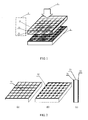
- FIG. 1 is a schematic structural view of the LCD panel capable of achieving low-temperature display, according to an embodiment of the present technical disclosure.
- the LCD panel comprises an opposing substrate 2, a thin film transistor (TFT) substrate 3 and a liquid crystal layer (not shown in FIG 1 ) disposed between the opposing substrate 2 and the TFT substrate 3.
- a backlight unit (backlight) is arranged on the back side of the LCD panel, so that the backlight 1 can be incident from the back side of the TFT substrate 3.
- the TFT substrate 3 includes: an electrical heating pattern 31, a TFT pattern 32 including the gate lines and the data lines, and a glass substrate 33.
- the TFT substrate (array substrate) of the embodiment of the present technical disclosure includes a plurality of gate lines and a plurality of data lines which are intersected with each other to define pixel units arranged in an array.
- each pixel unit includes a TFT working as a switching element and a pixel electrode configured to control the arrangement of liquid crystals.
- a gate electrode of is electrically connected or integrally formed with corresponding gate lines;
- a source electrode is electrically connected or integrally formed with corresponding data lines; and
- a drain electrode is electrically connected or integrally formed with a corresponding pixel electrode.
- the opposing substrate 2 is, for instance, a color filter substrate, which for instance comprises a black matrix and color filter units defined by the black matrix and corresponding to the pixel units of the TFT substrate.
- the opposing substrate 2 may be not provided with the color filter units.
- the electrical heating pattern 31 is, as illustrated in FIGS. 1 and 2(a) , disposed on the back side of the TFT substrate 3, namely the side into which the backlight 1 is incident, i.e., the side facing away from the liquid crystal layer.
- the TFT pattern 32 including the gate lines and the data lines is, as illustrated in FIGS. 1 and 2(b) , disposed on the front side of the TFT substrate 3, namely the side from which the backlight 1 is emitted out, i.e., the side facing the liquid crystal layer.
- the electrical heating pattern 31 corresponds to the TFT pattern 32 including the gate lines and the data lines, disposed on the front side of the TFT substrate 3.
- both the electrical heating pattern 31 and the TFT pattern 32 are overlapped with each other in a direction perpendicular to the LCD panel and have equivalent dimensions so that the electrical heating pattern cannot shield a display area in the TFT pattern.
- the electrical heating pattern may be made of a material which can emit heat under application of a voltage, such as Fe-Cr-Al alloy or Ni-Cr alloy.
- FIG. 2(c) which is a sectional view of the TFT substrate 3
- the electrical heating pattern 31 is disposed on one side of the glass substrate 33
- the TFT pattern 32 including the gate lines and the data lines is disposed on the other side.
- FIG. 3 is a schematic structural position diagram of the control circuit board and the temperature sensor on the TFT substrate of the embodiment of the present technical disclosure.
- the control circuit board 4 can be arranged on one side of the TFT substrate 3 on which the electrical heating pattern 31 is disposed, for instance, may be bonded on the TFT substrate 3 via conductive adhesive.
- a control circuit on the control circuit board 4 is connected with the electrical heating pattern 31.
- the bonding position of the control circuit board 4 may be similar to that of a drive circuit board of the TFT pattern on the TFT substrate.
- the control circuit board 4 is bonded on the substrate so that the light emitted by the backlight is not shielded and can completely pass through the display screen, and hence the transmittance cannot be affected.
- the temperature sensor 5 is arranged (by bonding, for instance) on the side wall of the TFT substrate 3 and connected with the control circuit on the control circuit board 4.
- the temperature sensor 5 can control the switching of the control circuit according to the difference between the ambient temperature and the temperature of the LCD panel, and hence achieve the aim of controlling the operation of the electrical heating pattern 31.
- the control circuit board 4 can be independently arranged, for instance, arranged into two or integrated into one, or integrated into the drive circuit board (printed circuit board assembly (PCBA)) (not shown in FIG. 3 ) of the TFT substrate.
- PCBA printed circuit board assembly
- both the temperature sensor 5 and the control circuit board 4 are light and thin elements, have low influence on the weight of the whole LCD panel, and will not affect the quality of the LCD panel basically.
- the LCD panel detects the ambient temperature and the temperature of the LCD panel through the temperature sensor 5.
- the control circuit can automatically apply a working voltage to the electrical heating pattern 31 so as to heat the LCD panel, and hence the LCD panel will continue to operate normally.
- the control circuit can automatically stop applying the working voltage to the electrical heating pattern 31 and protect the LCD panel from being overheated.
- the control circuit can also automatically stop heating the LCD panel so as to protect the LCD panel from being overheated, and hence the LCD panel can operate normally and the objective of energy conservation can be achieved.
- the opposing substrate in the LCD panel and the cell-assembly process can employ conventional ones in practice.
- the difference is the forming process of the TFT substrate.
- the processes can be conducted as follows.
- Step 1 forming an electrical heating pattern on one side of a base substrate, and forming a TFT pattern including gate lines and data lines on the other side of the base substrate.
- one layer of Fe-Cr-Al alloy or Ni-Cr alloy or the like is deposited on one side of the base substrate (for instance, a glass or plastic substrate) for forming an electrical heating film layer; secondly, a layer of photoresist is coated on the electrical heating film layer; and thirdly, the electrical heating pattern is formed by exposure, development, etching and photoresist removal.
- the process for forming the TFT pattern including gate lines and data lines on the other side of the base substrate comprises the following steps of: base substrate cleaning, film deposition, photoresist coating, exposure, development, etching and photoresist removal.
- the position of the electrical heating pattern and the pattern of the gate lines and the data lines can be controlled by alignment marks, so that the positions of the electrical heating pattern and the pattern of the gate lines and the data lines can surely correspond to each other.
- the electrical heating pattern may be formed at first, or the TFT pattern including the gate lines and the data lines may be formed at first.
- the electrical heating pattern can be formed at first, and hence the TFT pattern is formed.
- Step 2 arranging the control circuit board on one side of the TFT substrate on which the electrical heating pattern is disposed, and arranging the temperature sensor on the side wall of the TFT substrate.
- the control circuit on the control circuit board is electrically connected with the electrical heating pattern and the temperature sensor respectively.
- control circuit board may be bonded on one side of the TFT substrate, on which the electrical heating pattern is disposed, via conductive adhesive, and the temperature sensor may be bonded on the side wall of the TFT substrate.
- the control circuit on the control circuit board is connected with the electrical heating pattern, and the temperature sensor is electrically connected with the control circuit on the control circuit board.
- the temperature sensor controls the switching of the control circuit according to the difference between the ambient temperature and the temperature of the LCD panel, and hence controls the temperature of the electrical heating pattern.
- the electrical heating pattern corresponding to the gate lines and the data lines disposed on the front side of the substrate, is disposed on the back side of the TFT substrate by a patterning process.
- the patterned electrical heating pattern is combined with the control circuit board and the temperature sensor arranged so as to heat the LCD panel.
- the electrical heating pattern corresponds to the pattern of the gate lines and the data lines, the electrical heating pattern does not affect the transmittance of the display panel.
- the electrical heating pattern is combined with the control circuit board and the temperature sensor to heat the LCD panel, and hence the display function of the LCD panel at low temperature can be achieved.
- both the temperature sensor and the control circuit board provided with the control circuit are light and thin elements, have very small influence on the quality of the whole LCD panel, and do not affect the weight of the LCD panel basically.
- the LCD panel provided by the present technical disclosure has the advantages of light weight and small size.
Landscapes
- Physics & Mathematics (AREA)
- Nonlinear Science (AREA)
- Mathematical Physics (AREA)
- Chemical & Material Sciences (AREA)
- Crystallography & Structural Chemistry (AREA)
- General Physics & Mathematics (AREA)
- Optics & Photonics (AREA)
- Engineering & Computer Science (AREA)
- Microelectronics & Electronic Packaging (AREA)
- Liquid Crystal (AREA)
- Devices For Indicating Variable Information By Combining Individual Elements (AREA)
Abstract
Description
- An embodiment of the present technical disclosure relates to a liquid-crystal display (LCD) panel capable of achieving low-temperature display.
- Due to the characteristics of light weight, small thickness, good portability and the like, LCD panels have been widely applied to various domestic televisions and portable electronic products. A typical LCD panel usually can only operate normally around the normal temperature, so that general indoor workplaces can meet the display requirement. However, as for cold climate areas or workplaces at an extremely low temperature, as liquid crystal molecules at the low temperature cannot be deflected properly, the LCD panel cannot operate normally.
- In order to solve the problem of low-temperature display, the following methods have been proposed to achieve low-temperature liquid-crystal display:
- 1) An additional electrical heating element is arranged on the outside of the LCD panel, and heating to the display panel can be conducted through a control circuit. For instance, one layer of heating sleeve is attached on the back side of the whole LCD panel to heat the LCD panel, so that the LCD panel can display at a low temperature. However, as the electrical heating element has a big thickness and large weight in kilogram level, the structure will increase the overall thickness and the overall weight of the LCD panel.
- 2) A glass substrate, on which a indium tin oxide (ITO) transparent conductive film is deposited, is arranged between a backlight and a thin-film transistor (TFT) substrate, and the low-temperature display function can achieved by heating on the liquid crystal cell of the display panel with the transparent conductive film. However, as the ITO transparent conductive film has a poor heating effect, the heat which can be supplied to the liquid crystal cell may be very limited. In addition, as glass has poor heat conductibility, most heat produced by the ITO transparent conductive film is lost during the process of being transmitted to the liquid crystal cell via the heat transmission of the glass substrate. Therefore, by adoption of the structure, the heating effect of the LCD panel will be poor. Moreover, due to the glass substrate, the transmittance can be reduced and the weight of the LCD panel can be increased.
- 3) One layer of ITO film is deposited on the back side of the TFT substrate, and applying voltage to the ITO film to heat the display panel. By adoption of the method, the transmittance of the LCD panel will be reduced as well and the heating effect will be poor.
- An embodiment of the present technical disclosure provides an LCD panel capable of achieving low-temperature display, which can achieve low-temperature display in the case of not affecting the transmittance.
- According to one aspect of the present technical disclosure, an LCD panel capable of achieving low-temperature display is provided. The LCD panel comprises an opposing substrate, a thin film transistor (TFT) substrate and a liquid crystal cell disposed between the opposing substrate and the TFT substrate, a TFT pattern including gate lines and data lines is disposed on the front side of the TFT substrate, and an electrical heating pattern corresponding to the TFT pattern is disposed on the back side of the TFT substrate.
- For instance, the TFT substrate may further include: a control circuit board arranged on the same side with the electrical heating pattern and a temperature sensor arranged on a side wall of the TFT substrate; a control circuit on the control circuit board is respectively connected with the electrical heating pattern and the temperature sensor.
- For instance, the electrical heating pattern may be made of a material which can emit heat under application of a voltage.
- For instance, the material may be Fe-Cr-Al alloy or Ni-Cr alloy.
- For instance, the control circuit board may be bonded on the TFT substrate.
- For instance, the control circuit board may be bonded on the TFT substrate via conductive adhesive.
- For instance, the control circuit board is independently arranged or integrated into a drive circuit board of the TFT substrate.
- For instance, the temperature sensor may be bonded on the side wall of the TFT substrate.
- Further scope of applicability of the present technical disclosure will become apparent from the detailed description given hereinafter. However, it should be understood that the detailed description and specific examples, while indicating preferred embodiments of the technical disclosure, are given by way of illustration only, since various changes and modifications within the spirit and scope of the technical disclosure will become apparent to those skilled in the art from the following detailed description.
- The present technical disclosure will become more fully understood from the detailed description given hereinafter and the accompanying drawings which are given by way of illustration only, and thus are not limitative of the present technical disclosure and wherein:
-
FIG. 1 is a schematic structural view of an LCD panel capable of achieving low-temperature display, according to an embodiment of the present technical disclosure; -
FIG. 2(a) is a schematic structural view of an electrical heating pattern disposed on the back side of a TFT substrate according to an embodiment of the present technical disclosure; -
FIG. 2(b) is a schematic structural view of a TFT pattern disposed on the front side of the TFT substrate according to an embodiment of the present technical disclosure; -
FIG. 2(c) is a sectional view of the TFT substrate according to an embodiment of the present technical disclosure; and -
FIG 3 is a schematic structural position diagram of a control circuit board and a temperature sensor on the TFT substrate according to an embodiment of the present technical disclosure. - 1. Backlight; 2. Opposing Substrate; 3. TFT Substrate; 31. Electrical Heating Pattern; 32. TFT Pattern; 33. Glass Substrate; 4. Control Circuit Board; 5. Temperature Sensor.
- For more clear understanding of the objectives, technical solutions and advantages of the embodiments of the present technical disclosure, clear and complete description will be given below to the technical solutions of the embodiments of the present technical disclosure with reference to the accompanying drawings of the embodiments of the present technical disclosure. It will be obvious to those skilled in the art that the preferred embodiments are only partial embodiments of the present technical disclosure but not all the embodiments. All the other embodiments obtained by those skilled in the art without creative efforts on the basis of the embodiments of the present technical disclosure illustrated shall fall within the scope of protection of the present technical disclosure.
- In an LCD panel provided by the embodiment of the present technical disclosure, an electrical heating pattern corresponding to gate lines and data lines disposed on the front side of a TFT substrate is deposited on the back side of the TFT substrate by a patterning process and configured to heat the LCD panel through an additionally arranged control circuit board and an additionally arranged temperature sensor.
-
FIG. 1 is a schematic structural view of the LCD panel capable of achieving low-temperature display, according to an embodiment of the present technical disclosure. As illustrated inFIG. 1 , the LCD panel comprises an opposing substrate 2, a thin film transistor (TFT)substrate 3 and a liquid crystal layer (not shown inFIG 1 ) disposed between the opposing substrate 2 and theTFT substrate 3. A backlight unit (backlight) is arranged on the back side of the LCD panel, so that thebacklight 1 can be incident from the back side of theTFT substrate 3. TheTFT substrate 3 includes: anelectrical heating pattern 31, aTFT pattern 32 including the gate lines and the data lines, and aglass substrate 33. - The TFT substrate (array substrate) of the embodiment of the present technical disclosure includes a plurality of gate lines and a plurality of data lines which are intersected with each other to define pixel units arranged in an array. For instance, each pixel unit includes a TFT working as a switching element and a pixel electrode configured to control the arrangement of liquid crystals. For instance, as for the TFT of each pixel unit, a gate electrode of is electrically connected or integrally formed with corresponding gate lines; a source electrode is electrically connected or integrally formed with corresponding data lines; and a drain electrode is electrically connected or integrally formed with a corresponding pixel electrode. The opposing substrate 2 is, for instance, a color filter substrate, which for instance comprises a black matrix and color filter units defined by the black matrix and corresponding to the pixel units of the TFT substrate. When the color filter units is arranged on the TFT substrate, the opposing substrate 2 may be not provided with the color filter units.
- The
electrical heating pattern 31 is, as illustrated inFIGS. 1 and 2(a) , disposed on the back side of theTFT substrate 3, namely the side into which thebacklight 1 is incident, i.e., the side facing away from the liquid crystal layer. TheTFT pattern 32 including the gate lines and the data lines is, as illustrated inFIGS. 1 and 2(b) , disposed on the front side of theTFT substrate 3, namely the side from which thebacklight 1 is emitted out, i.e., the side facing the liquid crystal layer. - It can be seen from
FIGs. 1, 2(a) and 2(b) that: theelectrical heating pattern 31 corresponds to theTFT pattern 32 including the gate lines and the data lines, disposed on the front side of theTFT substrate 3. For instance, both theelectrical heating pattern 31 and theTFT pattern 32 are overlapped with each other in a direction perpendicular to the LCD panel and have equivalent dimensions so that the electrical heating pattern cannot shield a display area in the TFT pattern. The electrical heating pattern may be made of a material which can emit heat under application of a voltage, such as Fe-Cr-Al alloy or Ni-Cr alloy. As illustrated inFIG. 2(c) which is a sectional view of theTFT substrate 3, theelectrical heating pattern 31 is disposed on one side of theglass substrate 33, and theTFT pattern 32 including the gate lines and the data lines is disposed on the other side. -
FIG. 3 is a schematic structural position diagram of the control circuit board and the temperature sensor on the TFT substrate of the embodiment of the present technical disclosure. As illustrated inFIG. 3 , thecontrol circuit board 4 can be arranged on one side of theTFT substrate 3 on which theelectrical heating pattern 31 is disposed, for instance, may be bonded on theTFT substrate 3 via conductive adhesive. In addition, a control circuit on thecontrol circuit board 4 is connected with theelectrical heating pattern 31. The bonding position of thecontrol circuit board 4 may be similar to that of a drive circuit board of the TFT pattern on the TFT substrate. For instance, thecontrol circuit board 4 is bonded on the substrate so that the light emitted by the backlight is not shielded and can completely pass through the display screen, and hence the transmittance cannot be affected. Thetemperature sensor 5 is arranged (by bonding, for instance) on the side wall of theTFT substrate 3 and connected with the control circuit on thecontrol circuit board 4. In addition, thetemperature sensor 5 can control the switching of the control circuit according to the difference between the ambient temperature and the temperature of the LCD panel, and hence achieve the aim of controlling the operation of theelectrical heating pattern 31. Thecontrol circuit board 4 can be independently arranged, for instance, arranged into two or integrated into one, or integrated into the drive circuit board (printed circuit board assembly (PCBA)) (not shown inFIG. 3 ) of the TFT substrate. - Herein, both the
temperature sensor 5 and thecontrol circuit board 4 are light and thin elements, have low influence on the weight of the whole LCD panel, and will not affect the quality of the LCD panel basically. - During operation, the LCD panel detects the ambient temperature and the temperature of the LCD panel through the
temperature sensor 5. When the ambient temperature is lower than the normal operating temperature of the LCD panel, the control circuit can automatically apply a working voltage to theelectrical heating pattern 31 so as to heat the LCD panel, and hence the LCD panel will continue to operate normally. When the heating temperature of the LCD panel is overly high, namely higher than the normal operating temperature of the LCD panel, the control circuit can automatically stop applying the working voltage to theelectrical heating pattern 31 and protect the LCD panel from being overheated. For instance, when the ambient temperature is equal to the normal operating temperature of the LCD panel, the control circuit can also automatically stop heating the LCD panel so as to protect the LCD panel from being overheated, and hence the LCD panel can operate normally and the objective of energy conservation can be achieved. - Simple description will be given below to the method for manufacturing the LCD panel capable of achieving low-temperature display, provided by the embodiment of the present technical disclosure. The opposing substrate in the LCD panel and the cell-assembly process (for forming a liquid crystal cell) can employ conventional ones in practice. The difference is the forming process of the TFT substrate. The processes can be conducted as follows.
- Step 1: forming an electrical heating pattern on one side of a base substrate, and forming a TFT pattern including gate lines and data lines on the other side of the base substrate.
- In one example, firstly, one layer of Fe-Cr-Al alloy or Ni-Cr alloy or the like is deposited on one side of the base substrate (for instance, a glass or plastic substrate) for forming an electrical heating film layer; secondly, a layer of photoresist is coated on the electrical heating film layer; and thirdly, the electrical heating pattern is formed by exposure, development, etching and photoresist removal. The process for forming the TFT pattern including gate lines and data lines on the other side of the base substrate comprises the following steps of: base substrate cleaning, film deposition, photoresist coating, exposure, development, etching and photoresist removal. In the exposure process, the position of the electrical heating pattern and the pattern of the gate lines and the data lines can be controlled by alignment marks, so that the positions of the electrical heating pattern and the pattern of the gate lines and the data lines can surely correspond to each other.
- Here, the electrical heating pattern may be formed at first, or the TFT pattern including the gate lines and the data lines may be formed at first. However, in order to reduce the damage of the TFT pattern on the TFT substrate, the electrical heating pattern can be formed at first, and hence the TFT pattern is formed.
- Step 2: arranging the control circuit board on one side of the TFT substrate on which the electrical heating pattern is disposed, and arranging the temperature sensor on the side wall of the TFT substrate.
- The control circuit on the control circuit board is electrically connected with the electrical heating pattern and the temperature sensor respectively.
- In one example, the control circuit board may be bonded on one side of the TFT substrate, on which the electrical heating pattern is disposed, via conductive adhesive, and the temperature sensor may be bonded on the side wall of the TFT substrate. The control circuit on the control circuit board is connected with the electrical heating pattern, and the temperature sensor is electrically connected with the control circuit on the control circuit board. The temperature sensor controls the switching of the control circuit according to the difference between the ambient temperature and the temperature of the LCD panel, and hence controls the temperature of the electrical heating pattern.
- In the LCD panel capable of achieving low-temperature display, according to the embodiment of the present technical disclosure, the electrical heating pattern, corresponding to the gate lines and the data lines disposed on the front side of the substrate, is disposed on the back side of the TFT substrate by a patterning process. The patterned electrical heating pattern is combined with the control circuit board and the temperature sensor arranged so as to heat the LCD panel. As the electrical heating pattern corresponds to the pattern of the gate lines and the data lines, the electrical heating pattern does not affect the transmittance of the display panel. Moreover, the electrical heating pattern is combined with the control circuit board and the temperature sensor to heat the LCD panel, and hence the display function of the LCD panel at low temperature can be achieved.
- Moreover, both the temperature sensor and the control circuit board provided with the control circuit, in the present technical disclosure, are light and thin elements, have very small influence on the quality of the whole LCD panel, and do not affect the weight of the LCD panel basically. Compared with the conventional technology, the LCD panel provided by the present technical disclosure has the advantages of light weight and small size.
- The embodiment of the technical disclosure being thus described, it will be obvious that the same may be varied in many ways. Such variations are not to be regarded as a departure from the spirit and scope of the technical disclosure, and all such modifications as would be obvious to those skilled in the art are intended to be included within the scope of the following claims.
Claims (8)
- A liquid-crystal display (LCD) panel capable of achieving low-temperature display, comprising: an opposing substrate, a thin-film-transistor (TFT) substrate and a liquid crystal layer disposed between the opposing substrate and the TFT substrate,
wherein a TFT pattern including gate lines and data lines is disposed on a front side of the TFT substrate; and an electrical heating pattern corresponding to the TFT pattern is disposed on a back side of the TFT substrate. - The LCD panel capable of achieving low-temperature display according to claim 1, wherein the TFT substrate further includes: a control circuit board arranged on a same side with the electrical heating pattern and a temperature sensor arranged on a side wall of the TFT substrate,
wherein a control circuit on the control circuit board is respectively connected with the electrical heating pattern and the temperature sensor. - The LCD panel capable of achieving low-temperature display according to claim 1 or 2, wherein the electrical heating pattern is made of a material which can emit heat under application of a voltage.
- The LCD panel capable of achieving low-temperature display according to claim 3, wherein the material is Fe-Cr-Al alloy or Ni-Cr alloy.
- The LCD panel capable of achieving low-temperature display according to any one of claims 2 to 4, wherein the control circuit board is bonded on the TFT substrate.
- The LCD panel capable of achieving low-temperature display according to claim 5, wherein the control circuit board is bonded on the TFT substrate via conductive adhesive.
- The LCD panel capable of achieving low-temperature display according to claim 2 or 3, wherein the control circuit board is independently arranged or integrated into a drive circuit board of the TFT pattern.
- The LCD panel capable of achieving low-temperature display according to claim 2 or 3, wherein the temperature sensor is bonded on the side wall of the TFT substrate.
Applications Claiming Priority (1)
| Application Number | Priority Date | Filing Date | Title |
|---|---|---|---|
| CN201210508732.2A CN103852924A (en) | 2012-12-03 | 2012-12-03 | Liquid crystal display panel supporting low-temperature display |
Publications (2)
| Publication Number | Publication Date |
|---|---|
| EP2738597A1 true EP2738597A1 (en) | 2014-06-04 |
| EP2738597B1 EP2738597B1 (en) | 2017-10-18 |
Family
ID=49667080
Family Applications (1)
| Application Number | Title | Priority Date | Filing Date |
|---|---|---|---|
| EP13195005.7A Not-in-force EP2738597B1 (en) | 2012-12-03 | 2013-11-29 | Liquid-crystal display (LCD) panel capable of achieving low-temperature display |
Country Status (3)
| Country | Link |
|---|---|
| US (1) | US9104057B2 (en) |
| EP (1) | EP2738597B1 (en) |
| CN (1) | CN103852924A (en) |
Families Citing this family (7)
| Publication number | Priority date | Publication date | Assignee | Title |
|---|---|---|---|---|
| CN104950493B (en) | 2015-07-10 | 2018-03-23 | 合肥鑫晟光电科技有限公司 | A kind of substrate and display device |
| CN106814486B (en) * | 2015-11-30 | 2020-10-13 | 惠州市德赛西威汽车电子股份有限公司 | LCD screen capable of displaying at low temperature and heating method thereof |
| CN105929582A (en) * | 2016-06-20 | 2016-09-07 | 宜昌市微特电子设备有限责任公司 | Liquid crystal panel expanding module and liquid crystal panel heating method |
| CN107045218B (en) * | 2017-03-17 | 2020-06-09 | 京东方科技集团股份有限公司 | An adaptive heating film, display panel and liquid crystal display device |
| CN107367860B (en) * | 2017-08-25 | 2019-07-16 | 深圳市华星光电技术有限公司 | LCD assembly |
| CN110221468A (en) * | 2019-06-10 | 2019-09-10 | 北海惠科光电技术有限公司 | Display panel and its temperature-compensation method, display device |
| CN113189810A (en) * | 2021-04-29 | 2021-07-30 | 河北恒昱达电子有限公司 | Liquid crystal module based on ITO glass heating technology |
Citations (5)
| Publication number | Priority date | Publication date | Assignee | Title |
|---|---|---|---|---|
| WO2002013220A1 (en) * | 2000-08-04 | 2002-02-14 | Siemens Aktiengesellschaft | Switching device with a component consisting of a shape memory alloy and with means for heating the same; and corresponding joining technique |
| US20050073642A1 (en) * | 2003-10-07 | 2005-04-07 | American Panel Corporation, Lg.Philips Lcd Co., Ltd. | Flat panel display having integral heater, EMI shield, and thermal sensors |
| US20070012897A1 (en) * | 2005-07-15 | 2007-01-18 | Samsung Electronics Co., Ltd. | Temperature sensor for display device, thin film transistor array panel including the temperature sensor, liquid crystal display, driving circuit for liquid crystal display and flicker controlling system for liquid crystal display |
| JP2007147694A (en) * | 2005-11-24 | 2007-06-14 | Epson Imaging Devices Corp | Liquid crystal device and electronic equipment |
| US20090251397A1 (en) * | 2008-04-02 | 2009-10-08 | American Panel Corporation | Liquid crystal flat panel display with an integral heater of predeterminable capacity |
Family Cites Families (6)
| Publication number | Priority date | Publication date | Assignee | Title |
|---|---|---|---|---|
| DE10129862A1 (en) * | 2000-08-04 | 2002-02-21 | Siemens Ag | Switching device with a component made of a shape memory alloy and with means for heating it, as well as corresponding connection technology |
| KR100627387B1 (en) * | 2004-06-29 | 2006-09-21 | 삼성에스디아이 주식회사 | LCD and its driving method |
| KR100599756B1 (en) * | 2004-06-29 | 2006-07-12 | 삼성에스디아이 주식회사 | LCD and its driving method |
| CN2824088Y (en) * | 2005-09-30 | 2006-10-04 | 比亚迪股份有限公司 | Liquid crystal display with temp compensation |
| TWI337672B (en) * | 2006-10-27 | 2011-02-21 | Chimei Innolux Corp | Liquid crystal display |
| TWI372276B (en) * | 2007-06-20 | 2012-09-11 | Au Optronics Corp | Liquid crystal display and method for making the same |
-
2012
- 2012-12-03 CN CN201210508732.2A patent/CN103852924A/en active Pending
-
2013
- 2013-11-29 EP EP13195005.7A patent/EP2738597B1/en not_active Not-in-force
- 2013-12-02 US US14/093,592 patent/US9104057B2/en not_active Expired - Fee Related
Patent Citations (5)
| Publication number | Priority date | Publication date | Assignee | Title |
|---|---|---|---|---|
| WO2002013220A1 (en) * | 2000-08-04 | 2002-02-14 | Siemens Aktiengesellschaft | Switching device with a component consisting of a shape memory alloy and with means for heating the same; and corresponding joining technique |
| US20050073642A1 (en) * | 2003-10-07 | 2005-04-07 | American Panel Corporation, Lg.Philips Lcd Co., Ltd. | Flat panel display having integral heater, EMI shield, and thermal sensors |
| US20070012897A1 (en) * | 2005-07-15 | 2007-01-18 | Samsung Electronics Co., Ltd. | Temperature sensor for display device, thin film transistor array panel including the temperature sensor, liquid crystal display, driving circuit for liquid crystal display and flicker controlling system for liquid crystal display |
| JP2007147694A (en) * | 2005-11-24 | 2007-06-14 | Epson Imaging Devices Corp | Liquid crystal device and electronic equipment |
| US20090251397A1 (en) * | 2008-04-02 | 2009-10-08 | American Panel Corporation | Liquid crystal flat panel display with an integral heater of predeterminable capacity |
Also Published As
| Publication number | Publication date |
|---|---|
| US9104057B2 (en) | 2015-08-11 |
| US20140152937A1 (en) | 2014-06-05 |
| CN103852924A (en) | 2014-06-11 |
| EP2738597B1 (en) | 2017-10-18 |
Similar Documents
| Publication | Publication Date | Title |
|---|---|---|
| CN102436323B (en) | Display device associated with touch panel and producing method thereof | |
| US9104057B2 (en) | Liquid-crystal display (LCD) panel capable of achieving low-temperature display | |
| US9727195B2 (en) | Touch panel and method for fabricating the same | |
| US9098132B2 (en) | Line on glass type liquid crystal display device and method of fabricating the same | |
| US9007329B2 (en) | Liquid crystal display device including touch panel | |
| US20110304571A1 (en) | Liquid crystal display device associated with touch panel and method for fabricating the same | |
| EP2759865B1 (en) | Liquid crystal display panel and method for manufacturing the same | |
| US20080182184A1 (en) | Color filter substrate, manufacturing method thereof and liquid crystal display | |
| KR20030055856A (en) | Fabricated Method Of Liquid Crystal Display Apparatus Integrated Film Type Touch Panel | |
| KR101901253B1 (en) | Display Device integrating with Touch Screen and Method for Manufacturing the Same | |
| CN103676271B (en) | Display device and cap assembly | |
| KR101658149B1 (en) | Display Device Including Touch Panel | |
| JP2012242843A (en) | Liquid crystal display panel and driving method for the same | |
| US9335577B2 (en) | Display device and cover member | |
| US8368866B2 (en) | Liquid crystal display device having heat generating electrode | |
| US20150146145A1 (en) | Color liquid crystal display panel and manufacturing method thereof | |
| WO2021035847A1 (en) | Liquid crystal display panel and manufacturing method therefor, and bezel-less liquid crystal display device | |
| US7224419B2 (en) | Liquid crystal display device | |
| US20170242312A1 (en) | Display Panel and Display Device | |
| KR101747721B1 (en) | Liquid crystal display device and manufacturing method thereof | |
| US8717528B2 (en) | Liquid crystal display panel and liquid crystal display | |
| US20140333876A1 (en) | Color Filter Substrate And Indium-Tin-Oxide Film Pattern Structure And Manufacturing Method Thereof, And Liquid Crystal Display | |
| US20140071362A1 (en) | Liquid crystal display panel | |
| KR20050004547A (en) | Liquid crystal display panel | |
| CN121454823A (en) | Electronic devices |
Legal Events
| Date | Code | Title | Description |
|---|---|---|---|
| PUAI | Public reference made under article 153(3) epc to a published international application that has entered the european phase |
Free format text: ORIGINAL CODE: 0009012 |
|
| 17P | Request for examination filed |
Effective date: 20131129 |
|
| AK | Designated contracting states |
Kind code of ref document: A1 Designated state(s): AL AT BE BG CH CY CZ DE DK EE ES FI FR GB GR HR HU IE IS IT LI LT LU LV MC MK MT NL NO PL PT RO RS SE SI SK SM TR |
|
| AX | Request for extension of the european patent |
Extension state: BA ME |
|
| R17P | Request for examination filed (corrected) |
Effective date: 20141204 |
|
| RBV | Designated contracting states (corrected) |
Designated state(s): AL AT BE BG CH CY CZ DE DK EE ES FI FR GB GR HR HU IE IS IT LI LT LU LV MC MK MT NL NO PL PT RO RS SE SI SK SM TR |
|
| RIC1 | Information provided on ipc code assigned before grant |
Ipc: G02F 1/1333 20060101AFI20170221BHEP Ipc: G02F 1/1362 20060101ALI20170221BHEP Ipc: G02F 1/1335 20060101ALN20170221BHEP Ipc: G02F 1/1345 20060101ALI20170221BHEP |
|
| GRAP | Despatch of communication of intention to grant a patent |
Free format text: ORIGINAL CODE: EPIDOSNIGR1 |
|
| STAA | Information on the status of an ep patent application or granted ep patent |
Free format text: STATUS: GRANT OF PATENT IS INTENDED |
|
| RIC1 | Information provided on ipc code assigned before grant |
Ipc: G02F 1/1333 20060101AFI20170412BHEP Ipc: G02F 1/1335 20060101ALN20170412BHEP Ipc: G02F 1/1345 20060101ALI20170412BHEP Ipc: G02F 1/1362 20060101ALI20170412BHEP |
|
| INTG | Intention to grant announced |
Effective date: 20170509 |
|
| GRAS | Grant fee paid |
Free format text: ORIGINAL CODE: EPIDOSNIGR3 |
|
| GRAA | (expected) grant |
Free format text: ORIGINAL CODE: 0009210 |
|
| STAA | Information on the status of an ep patent application or granted ep patent |
Free format text: STATUS: THE PATENT HAS BEEN GRANTED |
|
| AK | Designated contracting states |
Kind code of ref document: B1 Designated state(s): AL AT BE BG CH CY CZ DE DK EE ES FI FR GB GR HR HU IE IS IT LI LT LU LV MC MK MT NL NO PL PT RO RS SE SI SK SM TR |
|
| REG | Reference to a national code |
Ref country code: GB Ref legal event code: FG4D |
|
| REG | Reference to a national code |
Ref country code: CH Ref legal event code: EP |
|
| REG | Reference to a national code |
Ref country code: AT Ref legal event code: REF Ref document number: 938453 Country of ref document: AT Kind code of ref document: T Effective date: 20171115 Ref country code: IE Ref legal event code: FG4D |
|
| REG | Reference to a national code |
Ref country code: FR Ref legal event code: PLFP Year of fee payment: 5 |
|
| REG | Reference to a national code |
Ref country code: DE Ref legal event code: R096 Ref document number: 602013028039 Country of ref document: DE |
|
| REG | Reference to a national code |
Ref country code: NL Ref legal event code: FP |
|
| REG | Reference to a national code |
Ref country code: LT Ref legal event code: MG4D |
|
| REG | Reference to a national code |
Ref country code: AT Ref legal event code: MK05 Ref document number: 938453 Country of ref document: AT Kind code of ref document: T Effective date: 20171018 |
|
| PG25 | Lapsed in a contracting state [announced via postgrant information from national office to epo] |
Ref country code: NO Free format text: LAPSE BECAUSE OF FAILURE TO SUBMIT A TRANSLATION OF THE DESCRIPTION OR TO PAY THE FEE WITHIN THE PRESCRIBED TIME-LIMIT Effective date: 20180118 Ref country code: LT Free format text: LAPSE BECAUSE OF FAILURE TO SUBMIT A TRANSLATION OF THE DESCRIPTION OR TO PAY THE FEE WITHIN THE PRESCRIBED TIME-LIMIT Effective date: 20171018 Ref country code: FI Free format text: LAPSE BECAUSE OF FAILURE TO SUBMIT A TRANSLATION OF THE DESCRIPTION OR TO PAY THE FEE WITHIN THE PRESCRIBED TIME-LIMIT Effective date: 20171018 Ref country code: ES Free format text: LAPSE BECAUSE OF FAILURE TO SUBMIT A TRANSLATION OF THE DESCRIPTION OR TO PAY THE FEE WITHIN THE PRESCRIBED TIME-LIMIT Effective date: 20171018 Ref country code: SE Free format text: LAPSE BECAUSE OF FAILURE TO SUBMIT A TRANSLATION OF THE DESCRIPTION OR TO PAY THE FEE WITHIN THE PRESCRIBED TIME-LIMIT Effective date: 20171018 |
|
| PG25 | Lapsed in a contracting state [announced via postgrant information from national office to epo] |
Ref country code: RS Free format text: LAPSE BECAUSE OF FAILURE TO SUBMIT A TRANSLATION OF THE DESCRIPTION OR TO PAY THE FEE WITHIN THE PRESCRIBED TIME-LIMIT Effective date: 20171018 Ref country code: HR Free format text: LAPSE BECAUSE OF FAILURE TO SUBMIT A TRANSLATION OF THE DESCRIPTION OR TO PAY THE FEE WITHIN THE PRESCRIBED TIME-LIMIT Effective date: 20171018 Ref country code: IS Free format text: LAPSE BECAUSE OF FAILURE TO SUBMIT A TRANSLATION OF THE DESCRIPTION OR TO PAY THE FEE WITHIN THE PRESCRIBED TIME-LIMIT Effective date: 20180218 Ref country code: AT Free format text: LAPSE BECAUSE OF FAILURE TO SUBMIT A TRANSLATION OF THE DESCRIPTION OR TO PAY THE FEE WITHIN THE PRESCRIBED TIME-LIMIT Effective date: 20171018 Ref country code: BG Free format text: LAPSE BECAUSE OF FAILURE TO SUBMIT A TRANSLATION OF THE DESCRIPTION OR TO PAY THE FEE WITHIN THE PRESCRIBED TIME-LIMIT Effective date: 20180118 Ref country code: GR Free format text: LAPSE BECAUSE OF FAILURE TO SUBMIT A TRANSLATION OF THE DESCRIPTION OR TO PAY THE FEE WITHIN THE PRESCRIBED TIME-LIMIT Effective date: 20180119 Ref country code: LV Free format text: LAPSE BECAUSE OF FAILURE TO SUBMIT A TRANSLATION OF THE DESCRIPTION OR TO PAY THE FEE WITHIN THE PRESCRIBED TIME-LIMIT Effective date: 20171018 |
|
| REG | Reference to a national code |
Ref country code: DE Ref legal event code: R097 Ref document number: 602013028039 Country of ref document: DE |
|
| PG25 | Lapsed in a contracting state [announced via postgrant information from national office to epo] |
Ref country code: CZ Free format text: LAPSE BECAUSE OF FAILURE TO SUBMIT A TRANSLATION OF THE DESCRIPTION OR TO PAY THE FEE WITHIN THE PRESCRIBED TIME-LIMIT Effective date: 20171018 Ref country code: SK Free format text: LAPSE BECAUSE OF FAILURE TO SUBMIT A TRANSLATION OF THE DESCRIPTION OR TO PAY THE FEE WITHIN THE PRESCRIBED TIME-LIMIT Effective date: 20171018 Ref country code: EE Free format text: LAPSE BECAUSE OF FAILURE TO SUBMIT A TRANSLATION OF THE DESCRIPTION OR TO PAY THE FEE WITHIN THE PRESCRIBED TIME-LIMIT Effective date: 20171018 Ref country code: DK Free format text: LAPSE BECAUSE OF FAILURE TO SUBMIT A TRANSLATION OF THE DESCRIPTION OR TO PAY THE FEE WITHIN THE PRESCRIBED TIME-LIMIT Effective date: 20171018 Ref country code: CH Free format text: LAPSE BECAUSE OF NON-PAYMENT OF DUE FEES Effective date: 20171130 Ref country code: LI Free format text: LAPSE BECAUSE OF NON-PAYMENT OF DUE FEES Effective date: 20171130 Ref country code: MC Free format text: LAPSE BECAUSE OF FAILURE TO SUBMIT A TRANSLATION OF THE DESCRIPTION OR TO PAY THE FEE WITHIN THE PRESCRIBED TIME-LIMIT Effective date: 20171018 |
|
| PLBE | No opposition filed within time limit |
Free format text: ORIGINAL CODE: 0009261 |
|
| STAA | Information on the status of an ep patent application or granted ep patent |
Free format text: STATUS: NO OPPOSITION FILED WITHIN TIME LIMIT |
|
| PG25 | Lapsed in a contracting state [announced via postgrant information from national office to epo] |
Ref country code: RO Free format text: LAPSE BECAUSE OF FAILURE TO SUBMIT A TRANSLATION OF THE DESCRIPTION OR TO PAY THE FEE WITHIN THE PRESCRIBED TIME-LIMIT Effective date: 20171018 Ref country code: IT Free format text: LAPSE BECAUSE OF FAILURE TO SUBMIT A TRANSLATION OF THE DESCRIPTION OR TO PAY THE FEE WITHIN THE PRESCRIBED TIME-LIMIT Effective date: 20171018 Ref country code: SM Free format text: LAPSE BECAUSE OF FAILURE TO SUBMIT A TRANSLATION OF THE DESCRIPTION OR TO PAY THE FEE WITHIN THE PRESCRIBED TIME-LIMIT Effective date: 20171018 Ref country code: LU Free format text: LAPSE BECAUSE OF NON-PAYMENT OF DUE FEES Effective date: 20171129 Ref country code: PL Free format text: LAPSE BECAUSE OF FAILURE TO SUBMIT A TRANSLATION OF THE DESCRIPTION OR TO PAY THE FEE WITHIN THE PRESCRIBED TIME-LIMIT Effective date: 20171018 |
|
| REG | Reference to a national code |
Ref country code: BE Ref legal event code: MM Effective date: 20171130 |
|
| REG | Reference to a national code |
Ref country code: IE Ref legal event code: MM4A |
|
| 26N | No opposition filed |
Effective date: 20180719 |
|
| PG25 | Lapsed in a contracting state [announced via postgrant information from national office to epo] |
Ref country code: MT Free format text: LAPSE BECAUSE OF NON-PAYMENT OF DUE FEES Effective date: 20171129 |
|
| REG | Reference to a national code |
Ref country code: FR Ref legal event code: PLFP Year of fee payment: 6 |
|
| PG25 | Lapsed in a contracting state [announced via postgrant information from national office to epo] |
Ref country code: IE Free format text: LAPSE BECAUSE OF NON-PAYMENT OF DUE FEES Effective date: 20171129 |
|
| PG25 | Lapsed in a contracting state [announced via postgrant information from national office to epo] |
Ref country code: BE Free format text: LAPSE BECAUSE OF NON-PAYMENT OF DUE FEES Effective date: 20171130 Ref country code: SI Free format text: LAPSE BECAUSE OF FAILURE TO SUBMIT A TRANSLATION OF THE DESCRIPTION OR TO PAY THE FEE WITHIN THE PRESCRIBED TIME-LIMIT Effective date: 20171018 |
|
| PG25 | Lapsed in a contracting state [announced via postgrant information from national office to epo] |
Ref country code: HU Free format text: LAPSE BECAUSE OF FAILURE TO SUBMIT A TRANSLATION OF THE DESCRIPTION OR TO PAY THE FEE WITHIN THE PRESCRIBED TIME-LIMIT; INVALID AB INITIO Effective date: 20131129 |
|
| PG25 | Lapsed in a contracting state [announced via postgrant information from national office to epo] |
Ref country code: CY Free format text: LAPSE BECAUSE OF NON-PAYMENT OF DUE FEES Effective date: 20171018 |
|
| PG25 | Lapsed in a contracting state [announced via postgrant information from national office to epo] |
Ref country code: MK Free format text: LAPSE BECAUSE OF FAILURE TO SUBMIT A TRANSLATION OF THE DESCRIPTION OR TO PAY THE FEE WITHIN THE PRESCRIBED TIME-LIMIT Effective date: 20171018 |
|
| PG25 | Lapsed in a contracting state [announced via postgrant information from national office to epo] |
Ref country code: TR Free format text: LAPSE BECAUSE OF FAILURE TO SUBMIT A TRANSLATION OF THE DESCRIPTION OR TO PAY THE FEE WITHIN THE PRESCRIBED TIME-LIMIT Effective date: 20171018 |
|
| PG25 | Lapsed in a contracting state [announced via postgrant information from national office to epo] |
Ref country code: PT Free format text: LAPSE BECAUSE OF FAILURE TO SUBMIT A TRANSLATION OF THE DESCRIPTION OR TO PAY THE FEE WITHIN THE PRESCRIBED TIME-LIMIT Effective date: 20171018 |
|
| PG25 | Lapsed in a contracting state [announced via postgrant information from national office to epo] |
Ref country code: AL Free format text: LAPSE BECAUSE OF FAILURE TO SUBMIT A TRANSLATION OF THE DESCRIPTION OR TO PAY THE FEE WITHIN THE PRESCRIBED TIME-LIMIT Effective date: 20171018 |
|
| PGFP | Annual fee paid to national office [announced via postgrant information from national office to epo] |
Ref country code: NL Payment date: 20201113 Year of fee payment: 8 |
|
| PGFP | Annual fee paid to national office [announced via postgrant information from national office to epo] |
Ref country code: DE Payment date: 20201118 Year of fee payment: 8 Ref country code: GB Payment date: 20201118 Year of fee payment: 8 Ref country code: FR Payment date: 20201013 Year of fee payment: 8 |
|
| REG | Reference to a national code |
Ref country code: DE Ref legal event code: R119 Ref document number: 602013028039 Country of ref document: DE |
|
| REG | Reference to a national code |
Ref country code: NL Ref legal event code: MM Effective date: 20211201 |
|
| GBPC | Gb: european patent ceased through non-payment of renewal fee |
Effective date: 20211129 |
|
| PG25 | Lapsed in a contracting state [announced via postgrant information from national office to epo] |
Ref country code: NL Free format text: LAPSE BECAUSE OF NON-PAYMENT OF DUE FEES Effective date: 20211201 |
|
| PG25 | Lapsed in a contracting state [announced via postgrant information from national office to epo] |
Ref country code: GB Free format text: LAPSE BECAUSE OF NON-PAYMENT OF DUE FEES Effective date: 20211129 Ref country code: DE Free format text: LAPSE BECAUSE OF NON-PAYMENT OF DUE FEES Effective date: 20220601 |
|
| PG25 | Lapsed in a contracting state [announced via postgrant information from national office to epo] |
Ref country code: FR Free format text: LAPSE BECAUSE OF NON-PAYMENT OF DUE FEES Effective date: 20211130 |