EP2733718A2 - Method and device for evaluating signals from an OSSD output element - Google Patents
Method and device for evaluating signals from an OSSD output element Download PDFInfo
- Publication number
- EP2733718A2 EP2733718A2 EP13005266.5A EP13005266A EP2733718A2 EP 2733718 A2 EP2733718 A2 EP 2733718A2 EP 13005266 A EP13005266 A EP 13005266A EP 2733718 A2 EP2733718 A2 EP 2733718A2
- Authority
- EP
- European Patent Office
- Prior art keywords
- circuit arrangement
- circuit
- ossd
- signal components
- output
- Prior art date
- Legal status (The legal status is an assumption and is not a legal conclusion. Google has not performed a legal analysis and makes no representation as to the accuracy of the status listed.)
- Granted
Links
Images

Classifications
-
- G—PHYSICS
- G05—CONTROLLING; REGULATING
- G05B—CONTROL OR REGULATING SYSTEMS IN GENERAL; FUNCTIONAL ELEMENTS OF SUCH SYSTEMS; MONITORING OR TESTING ARRANGEMENTS FOR SUCH SYSTEMS OR ELEMENTS
- G05B9/00—Safety arrangements
- G05B9/02—Safety arrangements electric
-
- G—PHYSICS
- G01—MEASURING; TESTING
- G01R—MEASURING ELECTRIC VARIABLES; MEASURING MAGNETIC VARIABLES
- G01R31/00—Arrangements for testing electric properties; Arrangements for locating electric faults; Arrangements for electrical testing characterised by what is being tested not provided for elsewhere
- G01R31/28—Testing of electronic circuits, e.g. by signal tracer
- G01R31/282—Testing of electronic circuits specially adapted for particular applications not provided for elsewhere
- G01R31/2829—Testing of circuits in sensor or actuator systems
-
- G—PHYSICS
- G01—MEASURING; TESTING
- G01R—MEASURING ELECTRIC VARIABLES; MEASURING MAGNETIC VARIABLES
- G01R31/00—Arrangements for testing electric properties; Arrangements for locating electric faults; Arrangements for electrical testing characterised by what is being tested not provided for elsewhere
- G01R31/327—Testing of circuit interrupters, switches or circuit-breakers
- G01R31/3277—Testing of circuit interrupters, switches or circuit-breakers of low voltage devices, e.g. domestic or industrial devices, such as motor protections, relays, rotation switches
-
- G—PHYSICS
- G01—MEASURING; TESTING
- G01R—MEASURING ELECTRIC VARIABLES; MEASURING MAGNETIC VARIABLES
- G01R31/00—Arrangements for testing electric properties; Arrangements for locating electric faults; Arrangements for electrical testing characterised by what is being tested not provided for elsewhere
- G01R31/50—Testing of electric apparatus, lines, cables or components for short-circuits, continuity, leakage current or incorrect line connections
Definitions
- the invention enables the monitoring of the wiring without special test pulses from the Circuit arrangements, in particular within secure input devices, in particular via their own test and / or clock outputs are required. If the monitoring of the wiring of the circuit arrangements, especially within secure input devices in the application is mandatory, it would be in a standard solution only by contact decoupling the OSSD outputs from the circuitry, eg via a safety relay, and the use of additional test and / or clock outputs possible. When using the proposed circuit, this decoupling can be omitted, as well as a cross-circuit monitoring by the detection dynamic signal components, and thus present by the detection of dynamic OSSD pulses.
- each of the devices includes a logic device 230 (FIG. Fig. 1 ) or 213, 230 '( Fig.2 ), to which the circuit output of the first circuit arrangement and the circuit output of the second circuit arrangement is connected, and which is formed, that of the first Circuit arrangement detected static signal components and to evaluate the detected by the second circuit dynamic signal components.
- a logic device 230 FIG. Fig. 1
- the evaluation of the static as well as the dynamic signal component and the information for further processing is processed accordingly.
- the logic device expediently also performs a comparison based on the static and dynamic signal components.
- the dynamics can be monitored on a line and combined with the static evaluation of the state, so that essentially all faults in the wiring can be covered.
Landscapes
- Physics & Mathematics (AREA)
- General Physics & Mathematics (AREA)
- Engineering & Computer Science (AREA)
- Automation & Control Theory (AREA)
- Tests Of Electronic Circuits (AREA)
- Testing, Inspecting, Measuring Of Stereoscopic Televisions And Televisions (AREA)
Abstract
Die Erfindung betrifft ein Verfahren zur Auswertung von Signalen, die von einem OSSD-Ausgangsschaltelement kommen. Das Verfahren beinhaltet die Schritte des separaten Erfassens von statischen und dynamischen Signalanteile von, von einem OSSD-Ausgangsschaltelement (100) kommenden Signalen, und das Auswerten der statischen Signalanteile sowie Auswerten der dynamischen Signalanteile.The invention relates to a method for evaluating signals coming from an OSSD output switching element. The method includes the steps of separately acquiring static and dynamic signal components from signals coming from an OSSD output switching element (100), and evaluating the static signal components and evaluating the dynamic signal components.
Description
Die Erfindung betrifft ein Verfahren und eine Schaltung zur Auswertung von Signalen, die von einem OSSD-Ausgangsschaltelement kommen.The invention relates to a method and a circuit for evaluating signals coming from an OSSD output switching element.
Zur Reduzierung eines Risikos für Mensch oder Umwelt werden insbesondere in automatisierten Anlagen Sicherheitsfunktionen realisiert. Einfache Beispiele hierfür sind die Abschaltung einer Maschine nach Drücken eines Not-Aus-Tasters oder das Anhalten eines Roboters, wenn eine Person in den Sicherheitsbereich des Roboters eintritt und dabei z.B. eine Lichtschranke unterbricht oder von einem ein Lichtgitter erfasst wird, welches den Sicherheitsbereich des Roboters überwacht oder eine überwachte Zugangstür öffnet. Bei besonders sicherheitskritischen Prozessen kann es auch erforderlich sein, größere Teile einer komplexen Anlage oder sogar die gesamte Anlage herunter zu fahren, wenn bestimmte Sicherheitsfunktionen aktiviert werden.In order to reduce the risk to people or the environment, safety functions are implemented, especially in automated systems. Simple examples of this are the shutdown of a machine after pressing an emergency stop button or the stopping of a robot when a person enters the safety area of the robot, while e.g. a photocell interrupts or is detected by a light grid, which monitors the safety area of the robot or opens a monitored access door. In the case of very safety-critical processes, it may also be necessary to shut down larger parts of a complex system or even the entire system if certain safety functions are activated.
Hierfür wird sicherheitsgerichtete Technik bzw. Sicherheitstechnik eingesetzt. Im Allgemeinen realisiert die Anwendung von Sicherheitstechnik einerseits die eigentliche Sicherheitsfunktion wie z.B. Not-Aus-Schaltung, Zweihand-Schaltung, Betriebsartenwahlschalter etc., zum anderen umfasst die Sicherheitstechnik fehlererkennende und/oder fehlerbeherrschende Maßnahmen z.B. nach in Standards festgelegten Sicherheitsanforderungen (z.B. nach IEC 61508, ISO 13849 etc.). Diese Sicherheitsanforderungen sind dem Fachmann grundsätzlich bekannt.For this purpose, safety-oriented technology or safety technology is used. In general, the application of safety technology on the one hand realizes the actual safety function such as emergency stop circuit, two-hand circuit, mode selector, etc., on the other hand, the safety technology includes error-detecting and / or erroneous measures such as in Standards defined safety requirements (eg according to IEC 61508, ISO 13849 etc.). These safety requirements are generally known to the person skilled in the art.
Innerhalb der Sicherheitstechnik zu deren Umsetzung eingesetzte Geräte und/oder Signale, welche den Sicherheitsanforderungen entsprechen, werden im Rahmen der Erfindung als sichere Geräte bzw. sichere Signale bezeichnet.Within the safety technology used for their implementation devices and / or signals that meet the safety requirements are referred to in the invention as safe devices or safe signals.
Insbesondere im Bereich der Sicherheitstechnik werden oft auch OSSD-Ausgangsschaltelemente (OSSD, Output Signal Switching Device) benötigt, die interne Ausgangsschaltkreise beinhalten, die entsprechend der Sicherheitsanforderungen getestet werden müssen.Especially in the area of safety engineering, OSSD output switching elements (OSSD) are often required, which contain internal output circuits which have to be tested according to the safety requirements.
Die Diagnose der Abschaltfähigkeit der Ausgangsschaltkreise erfolgt in der Regel durch kurzes Abschalten der diesen zugeordneten Ausgangstreibern. Die hierbei verwendeten Abschaltimpulse sind jedoch an den, die jeweiligen Auagangsschaltkreise abschließenden Ausgangsklemmen sichtbar. Möchte man die Ausgänge von OSSD-Ausgangsschaltelementen, nachfolgend als OSSD-Ausgänge bezeichnet, daher an die Eingänge von Eingangsgeräten anschließen, entsteht folglich, insbesondere im Falle von sicheren Eingangsgeräten, die Notwendigkeit, dass diese sichtbaren Abschaltimpulse durch einen Eingangsfilter des Eingangsgerätes kommen und aufgrund der Sichtbarkeit ausgefiltert werden müssen.The diagnosis of the turn-off of the output circuits is usually done by briefly switching off the associated output drivers. However, the shutdown pulses used in this case are visible to the, the respective Auagangsschaltkreise final output terminals. Therefore, if one wishes to connect the outputs of OSSD output switching elements, hereinafter referred to as OSSD outputs, to the inputs of input devices, it becomes necessary, especially in the case of safe input devices, for these visible switch-off pulses to pass through an input filter of the input device and for the Visibility must be filtered out.
Typische sichere Eingangsgeräte verwenden nach heutigem Stand der Technik in der Regel ferner eigene Testausgänge zur Überwachung einer externen Verkabelung. Dabei werden Testimpulse der Testausgänge wiederum in den Eingangsgeräten erfasst. Sollten diese ausbleiben, bedeutet das, dass ein Querschluss in der Verkabelung vorliegt und die Eingangsgeräte entsprechend reagieren müssen, und also insbesondere in dem Fall von sicheren Eingangsgeräten einen sicheren Zustand einnehmen müssen.Typical state-of-the-art input devices typically also use their own test outputs to monitor external cabling. It will be Test pulses of the test outputs in turn detected in the input devices. If these fail, this means that there is a cross-circuit in the cabling and the input devices must react accordingly, and thus have to assume a safe state, in particular in the case of safe input devices.
Wenn die Eingänge der Eingangsgeräte mit den OSSD-Ausgängen verbunden werden, kann das Eingangsgerät keine Überprüfung der Verdrahtung über die eigenen Testausgänge vornehmen, da diese nicht mit den OSSD-Ausgängen verschaltbar sind. Das heißt, die Eingangsgeräte haben keine Diagnose über die Verkabelung, was in vielen Applikationen nicht zulässig ist. Es bleibt dann nur zu hoffen, dass die Diagnose der OSSD-Ausgänge ausreicht und diese im Fehlerfall einen vorbestimmten, insbesondere sicheren zustand einnehmen. Dies ist z.B. bei einem Querschluss zu 24V nicht möglich, da die OSSD-Ausgänge in diesem Fehlerfall überbrückt sind. Bei vielen Applikationen muss deswegen dieser Fehlerfall durch eine sichere Verkabelung der Leitungen ausgeschlossen werden, was zusätzlich auch für erhöhte Kosten verursacht.If the inputs of the input devices are connected to the OSSD outputs, the input device can not check the wiring via its own test outputs, as these can not be interconnected with the OSSD outputs. This means that the input devices do not have diagnostics via the cabling, which is not permitted in many applications. It then remains to be hoped that the diagnosis of the OSSD outputs will be sufficient and that they assume a predetermined, especially safe state in the event of a fault. This is e.g. with a cross-circuit to 24V not possible because the OSSD outputs are bridged in this case of error. In many applications, therefore, this fault must be excluded by a secure wiring of the lines, which also causes additional costs.
Aus der
Eine Aufgabe der Erfindung ist es daher, einen gegenüber dem aufgezeigten Stand der Technik verbesserten Weg aufzuzeigen, mit welchem eine effektive Überwachung auf Fehler in der Verkabelung für den Fall bereitgestellt werden kann, wenn Eingänge von Schaltungsanordnungen, insbesondere von sicheren Eingangsgeräten, mit OSSD-Ausgängen zu verbinden sind.It is therefore an object of the invention to provide an improved way, over the cited prior art, of providing effective cabling fault monitoring in the event of inputs from circuitry, particularly from secure input devices, having OSSD outputs to connect.
Die Lösung der Erfindung ist mit einem Gegenstand mit den Merkmalen nach einem der unabhängigen Ansprüche gegeben. Bevorzugte oder zweckmäßige Ausführungsformen und Weiterbildungen sind Gegenstand der Unteransprüche.The solution of the invention is given with an article having the features of one of the independent claims. Preferred or expedient embodiments and developments are subject of the dependent claims.
Die Erfindung schlägt demgemäß ein Verfahren zur Auswertung von Signalen, die von einem OSSD-Ausgangsschaltelement kommen, vor, bei welchem die statischen und dynamischen Signalanteile von, von einem OSSD-Ausgangsschaltelement kommenden Signalen separat erfasst werden und anschließend ausgewertet werden.The invention accordingly proposes a method for evaluating signals coming from an OSSD output switching element in which the static and dynamic signal components of signals coming from an OSSD output switching element are separately detected and subsequently evaluated.
Entsprechend schlägt die Erfindung ferner eine insbesondere zur Durchführung des Verfahrens ausgebildete Vorrichtung vor, die zur Auswertung von Signalen, die von einem OSSD-Ausgangsschaltelement kommen, eine erste Schaltungsanordnung besitzt, welche mit deren Schaltungseingang an den Ausgang eines OSSD-Ausgangsschaltelement anzuschalten ist, wobei die erste Schaltungsanordnung eine Filtereinrichtung besitzt, die ausgebildet ist, statische Signalanteile zu erfassen und dynamische Signalanteile auszufiltern, und eine zweite Schaltungsanordnung besitzt, welche mit deren Schaltungseingang parallel zur ersten Schaltungsanordnung gleichermaßen an den Ausgang des OSSD-Ausgangsshaltelement anzuschalten ist, wobei die zweite Schaltungsanordnung eine Filtereinrichtung besitzt, die ausgebildet ist, dynamische Signalanteile zu erfassen und statische Signalanteile auszufiltern. Die erfindungsgemäße Schaltung besitzt ferner eine Logikvorrichtung, wobei der Schaltungsausgang der ersten Schaltungsanordnung und der Schaltungsausgang der zweiten Schaltungsanordnung mit der Logikvorrichtung verbunden ist, und wobei die Logikvorrichtung ausgebildet ist, die von der ersten Schaltungsanordnung erfassten statischen Signalanteile und die von der zweiten Schaltungsanordnung erfassten dynamischen Signalanteile auszuwerten.Accordingly, the invention further proposes a device designed in particular for carrying out the method, which, for the evaluation of signals coming from an OSSD output switching element, has a first circuit arrangement which is to be connected with its circuit input to the output of an OSSD output switching element, wherein the First circuit arrangement has a filter device which is designed to detect static signal components and filter out dynamic signal components, and has a second circuit arrangement, which with its circuit input parallel to the first circuit arrangement equally to be connected to the output of the OSSD output stop element, wherein the second circuit arrangement has a filter device which is designed to detect dynamic signal components and to filter out static signal components. The inventive circuit further comprises a logic device, wherein the circuit output of the first circuit arrangement and the circuit output of the second circuit arrangement is connected to the logic device, and wherein the logic device is formed, the static signal components detected by the first circuit arrangement and the dynamic signal components detected by the second circuit arrangement evaluate.
Durch die separate Erfassung sowohl der statischen und dynamischen Signalanteile von Signalen, die von einem OSSD-Ausgangsschaltelement kommen, und deren anschließenden Auswertung, den Signals separat erfasst werden und anschließend ausgewertet werden, ermöglich die Erfindung die Überwachung der Verkabelung, ohne dass spezielle Testimpulse von den Schaltungsanordnungen, insbesondere innerhalb von sicheren Eingangsgeräten, insbesondere über eigene Test- und/oder Taktausgänge erforderlich sind. Falls die Überwachung der Verkabelung der Schaltungsanordnungen, insbesondere innerhalb von sicheren Eingangsgeräten in der Applikation zwingend erfordert ist, wäre es in einer Standardlösung nur mittels kontaktbehafteter Entkopplung der OSSD-Ausgänge von den Schaltungsanordnungen, z.B. über ein Sicherheitsrelais, und der Verwendung zusätzlicher Test- und/oder Taktausgänge möglich. Bei Verwendung der vorgeschlagenen Schaltung kann diese Entkopplung entfallen, da auch eine Querschlussüberwachung durch die Erfassung dynamischer Signalanteile, und folglich durch die Erfassung von dynamischen OSSD-Impulsen vorhanden ist.By separately detecting both the static and dynamic signal components of signals coming from an OSSD output switching element, and their subsequent evaluation, the signals are detected separately and then evaluated, the invention enables the monitoring of the wiring without special test pulses from the Circuit arrangements, in particular within secure input devices, in particular via their own test and / or clock outputs are required. If the monitoring of the wiring of the circuit arrangements, especially within secure input devices in the application is mandatory, it would be in a standard solution only by contact decoupling the OSSD outputs from the circuitry, eg via a safety relay, and the use of additional test and / or clock outputs possible. When using the proposed circuit, this decoupling can be omitted, as well as a cross-circuit monitoring by the detection dynamic signal components, and thus present by the detection of dynamic OSSD pulses.
Von Vorteil ist ferner, dass die Filtereinrichtung der ersten Schaltungsanordnung aus Hardwareelementen aufgebaut ist oder softwarebasiert aufgebaut sein kann, so dass eine hohe Flexibilität bei der Auslegung der Filtereinrichtung vorhanden ist und also anwendungsspezifisch eine einstellbare Filterzeit zur Ausfilterung von OSSD-Impulsen zur Erfassung der statischen Signalzustände in der ersten Schaltungsanordnung ermöglicht.A further advantage is that the filter device of the first circuit arrangement is constructed of hardware elements or software-based, so that a high flexibility in the design of the filter device is present and thus application specific an adjustable filter time for filtering OSSD pulses for detecting the static signal states enabled in the first circuit arrangement.
Gemäß einer zweckmäßigen Ausführungsform besitzt die zweite Schaltungsanordnung ferner einen Spannungsteiler zur Signalanpassung eines am Schaltungseingang der zweiten Schaltungsanordnung anliegenden Signals.According to an expedient embodiment, the second circuit arrangement further has a voltage divider for signal matching of a signal applied to the circuit input of the second circuit arrangement.
Gemäß einer zweckmäßigen Ausführungsform besitzt die zweite Schaltungsanordnung einen Kondensator zum Ausfiltern der statischen Signalanteile und einen Optokoppler zur Übertragung von dynamischen Signalanteilen in Richtung der Logikvorrichtung, wobei bevorzugt zwischen dem Optokoppler und der Logikvorrichtung eine Signalanpassungseinrichtung angeordnet ist, die zur Signalanpassung eines von dem Optokoppler erhaltenen Signals ausgebildet ist.According to an expedient embodiment, the second circuit arrangement has a capacitor for filtering out the static signal components and an opto-coupler for transmitting dynamic signal components in the direction of the logic device, preferably a signal conditioning device being arranged between the optical coupler and the logic device for signal matching of a signal obtained from the optocoupler is trained.
Gemäß einer bevorzugten Ausführungsform ist die erste und die zweite Schaltungsanordnung Teil eines gemeinsamen Eingangsgerätes.According to a preferred embodiment, the first and the second circuit arrangement is part of a common input device.
Gemäß einer weiteren bevorzugten Ausführungsform ist die erste Schaltungsanordnung Teil eines Eingangsgerätes und die zweite Schaltungsanordnung Teil eines zum Eingangsgerät parallel geschalteten zweiten Gerätes, insbesondere eines Klemmengerätes, z.B. einer Diagnoseklemme, welches sehr einfach nachträglich installiert werden kann und eine Sicherheitsfunktion der ersten Schaltungsanordnung nicht beeinflusst und darüber hinaus sich z.B. auch selbst aus OSSD-Ausgangssignalen mit Energie versorgen kann, was den Verkabelungsaufwand noch weiter reduziert.According to a further preferred embodiment, the first circuit arrangement is part of an input device and the second circuit arrangement is part of an input device parallel connected second device, in particular a terminal device, such as a diagnostic terminal, which can be installed very easily and does not affect a safety function of the first circuit and beyond, for example, even from OSSD output signals can provide energy, which reduces the cabling effort even further ,
Weitere Merkmale und Vorteile der Erfindung werden aus der nachfolgenden, lediglich als beispielhaft zu betrachtenden Beschreibung von bevorzugten Ausführungsformen unter Bezugnahme auf den beigefügten Zeichnungen ersichtlich, wobei in den Zeichnungen zeigen:
-
Fig. 1 ein beispielhafter, im Rahmen der Erfindung liegender Aufbau eines Eingangsgerätes mit einer bevorzugten Ausführungsform einer Vorrichtung zur Signalerfassung und zur dynamischen Überwachung von Testimpulse an OSSD-Ausgängen, und -
Fig. 2 eine zurFig. 1 alternative, weitere bevorzugte Ausführungsform, basierend auf einer Realisierung mittels einer Diagnoseklemme in Kombination mit einem Eingangsgerät.
-
Fig. 1 an exemplary, within the scope of the invention lying construction of an input device with a preferred embodiment of a device for signal detection and for the dynamic monitoring of test pulses at OSSD outputs, and -
Fig. 2 one toFig. 1 alternative, further preferred embodiment, based on a realization by means of a diagnostic terminal in combination with an input device.
Nachfolgend wird auf die
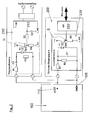
Hierzu umfasst jede der Vorrichtungen gemäß der Ausführungsformen nach
Ferner umfasst jede der Vorrichtungen jeweils eine zweite Schaltungsanordnung 210 (
Ferner umfasst jede der Vorrichtungen eine Logikvorrichtung 230 (
Gemäß Ausführungsform nach
Gemäß Ausführungsform nach
Während bei einer Ausführungsform nach
Wie den Ausführungsformen nach
Als erste Schaltungsanordnung, welche mit deren Schaltungseingang an den OSSD-Ausgang 110 und 120 des OSSD-Ausgangsschaltelement 100 anzuschalten ist kann vorteilhaft grundsätzlich jede digitale Eingangsschaltung eingesetzt werden, die zur Erfassung von Eingangssignalen geeignet ist, bzw. die innerhalb eines sicheren Eingangsgerätes zur Erfassung von sicheren Eingangssignalen geeignet ist. Wie bereits aufgezeigt, ist die Aufgabe dieser ersten Schaltungsanordnung 220, 220' ist, die vom OSSD-Ausgang 110 kommenden Signale statisch zu erfassen. Die dynamischen Anteile dieser Signale können innerhalb der erfindungsgemäßen Vorrichtung entweder durch die Auslegung der Filtereinrichtung in der Hardware dieser ersten Schaltungsanordnung 220, 220' oder in der Firmware der Logikvorrichtung 200 bzw. der Logikeinrichtung 230' ausgefiltert werden. Die Filterzeit ist hierbei zweckmäßig parametrierbar, um eine hohe Flexibilität zu erreichen.As the first circuit arrangement which is to be connected with its circuit input to the OSSD
Gemäß den Figuren weist die innerhalb des Eingangsgeräts 200 integrierte erste Schaltungsanordnung 220 als Filtereinrichtung zweckmäßig zunächst einen Spannungsteiler auf, der im dargestellten Fall aus zwei Widerständen R1 und R2 gebildet ist. Nach Anschalten der ersten Schaltungsanordnung 220 bzw. 220' mit deren Schaltungseingang an den Ausgang 110, 120 des OSSD-Ausgangsschaltelements 100 ist der Widerstand R1 ferner mit dem OSSD-Ausgang 110 und der Widerstand R2 ferner mit dem OSSD-Ausgang 120 verbunden. Zum Ausfiltern der dynamischen Signalanteile ist ein Kondensator C1 vorgesehen, der innerhalb der ersten Schaltungsanordnung 220 zwischen dem OSSD-Ausgang 110 und dem OSSD-Ausgang 120 angeordnet ist. Im Fall des obigen Spanungsteilers ist der Kondensator C1 somit zweckmäßig parallel zum Widerstand R2 geschaltet. Dem Kondensator C1 bzw. dem Widerstand R2 und dem Kondensator C1 ist wiederum parallel ein Optokoppler IC1 geschaltet, derart, dass eine auf der Eingangsseite des Optokopplers IC1 befindliche Leuchtdiode mit dem über den Spannungsteiler angepassten Signal angesteuert wird, wobei über den Kondensator C1 dynamischen Signalanteile ausgefiltert sind und die statischen Signalanteile zur weiteren Verwendung ausgekoppelt werden. Über den Spannungsteiler kann somit eine Signalanpassung der von dem OSSD-Ausgangsschaltelement 100 kommenden Signale für den Optokoppler IC1 vorgenommen werden. Am Ausgang des Optokopplers IC1 können dann mit Hilfe einer Gleichspannung von z.B. 3.3V und einem mit Masse "L_GND" verbundenen Abschlusswiderstand R3, parallel zum Widerstand R3 Signale abgegriffen werden, welche den statischen Signalanteilen von den Signalen entsprechen, die von dem OSSDAusgangsschaltelement 100 kommen. An diesem Abgreifpunkt "S" ist daher die Logikvorrichtung 230 gemäß
Auch die zweite Schaltungsanordnung 210 oder 210' als Filtereinrichtung zweckmäßig zunächst einen Spannungsteiler auf, der im dargestellten Fall aus zwei Widerständen R4 und R5 gebildet ist. Nach Anschalten der zweiten Schaltungsanordnung 210 bzw. 210' mit deren Schaltungseingang an den Ausgang 110, 120 des OSSD-Ausgangsschaltelements 100 ist der Widerstand R4 somit ferner mit dem OSSD-Ausgang 110 und der Widerstand R5 somit ferner mit dem OSSD-Ausgang 120 verbunden. Zum Ausfiltern der statischen Signalanteile weist die Filtereinrichtung der zweiten Schaltungsanordnung 210 bzw. 210' einen Kondensator C2 auf, der somit zweckmäßig zwischen dem Widerstand R4 und dem Widerstand R5 geschaltet ist, sowie einen Optokoppler IC2 zur Übertragung von dynamischen Signalanteilen in Richtung der Logikvorrichtung. Eine auf der Eingangsseite des Optokopplers IC2 befindliche Leuchtdiode ist im Signalpfad des Kondensators C2 diesem nachgeschaltet und also gemäß Figuren auch parallel zum Widerstand R5 geschaltet, derart also, dass die auf der Eingangsseite des Optokopplers IC2 befindliche Leuchtdiode mit dem über den Spannungsteiler angepassten Signal angesteuert wird, wobei über den Kondensator C2 die statischen Signalanteile ausgefiltert sind und die dynamischen Signalanteile zur weiteren Verwendung ausgekoppelt werden. Über den Spannungsteiler kann somit eine Signalanpassung der von dem OSSD-Ausgangsschaltelement 100 kommenden Signale für den Optokoppler IC2 vorgenommen werden. Am Ausgang des Optokopplers IC2 können dann mit Hilfe einer Gleichspannung von z.B. 3.3V und einem mit Masse "L_GND" verbundenen Abschlusswiderstand R6, parallel zum Widerstand R6 Signale abgegriffen werden, welche den dynamischen Signalanteilen von den Signalen entsprechen, die von dem OSSD-Ausgangsschaltelement 100 kommen. An diesem Abgreifpunkt "D" ist daher ein weiterführender Signalpfad zur Logikvorrichtung 230 (
Über die aus den Widerständen R6 und R7 sowie dem Kondensator C3 aufgebaute Signalanpassungseinrichtung können die abgegriffenen Signale an die jeweilige spezifische innere Struktur der Logikvorrichtung 230 (
In der Logikvorrichtung 230 bzw. den Logikeinrichtungen 230' und 213 erfolgt sodann die Auswertung der statischen als auch der dynamischen Signalanteil und die Information für die weitere Verarbeitung, z.B. in einer nicht dargestellten, über ein Netzwerk mit der Logikvorrichtung 230 verbundenen Sicherheitssteuerung, wird entsprechend aufbereitet.In the
Gemäß Ausführungsform nach
Die Ausführungsform nach
Wie vorstehend aufgezeigt, kann gemäß Ausführungsform nach
As indicated above, according to embodiment can
Die gemäß Erfindung vorgeschlagene Lösung, welche vorstehend unter Bezugnahme auf die zwei bevorzugten Ausführungsformen nach
Hierdurch kann eine Überwachung der Verkabelung durchgeführt werden, ohne dass spezielle Testimpulse von einem Eingangsgerät erforderlich sind. Falls die Überwachung der Verkabelung im Eingangsgerät in der Applikation zwingen erfordert ist, wäre es in einer Standardlösung nur mittels kontaktbehafteter Entkopplung der OSSD-Ausgänge vom Eingangsgerät, z.B. mittels eines Sicherheitsrelais, und Verwendung zusätzlicher Test- bzw. Taktausgänge des Eingangsgerätes möglich. Bei Verwendung der vorgeschlagenen Lösung nach der Erfindung kann diese Entkopplung entfallen, da eine Querschlussüberwachung durch die dynamische Erfassung von OSSD-Impulsen gewährleistet werden kann.This allows monitoring of the cabling without requiring special test pulses from an input device. If monitoring of the cabling in the input device is required in the application, it would only be possible in a standard solution by means of contact-based decoupling of the OSSD outputs from the input device, e.g. by means of a safety relay, and use of additional test or clock outputs of the input device possible. When using the proposed solution according to the invention, this decoupling can be omitted, since a cross-circuit monitoring can be ensured by the dynamic detection of OSSD pulses.
Ferner können sehr schnelle OSSD-Impulse, z.B. bei Lichtschranken im µs Bereich, unabhängig von der statischen Signalerfassung kostengünstig überwacht werden und erfordern keine sehr schnelle Schaltungsanordnung oder Logikverarbeitung, die schnell genug sind, um die kurzen Testimpulse zu erfassen, da die zweite Schaltungsanordnung durch Dimensionierung der ausgangsseitig zum Optokoppler IC angeordneten Signalanpassungseinrichtung, gemäß
Ferner wird durch die Erfassung der dynamischen Signalanteile auch das Verhalten der OSSD-Ausgänge mit überwacht. Bleiben z.B. die Impulse bei dauerhaftem High-Signal aus, spricht dies für einen Querschluss auf 24V oder für einen defekten OSSD-Ausgang. Diese Überwachung wäre mit einer Standardschaltung nicht möglich, was ein Sicherheitsrisiko darstellt.Furthermore, the behavior of the OSSD outputs is also monitored by the acquisition of the dynamic signal components. Stay e.g. the pulses at a sustained high signal, this speaks for a cross-circuit to 24V or for a defective OSSD output. This monitoring would not be possible with a standard circuit, which is a security risk.
Ferner besteht eine flexible Anpassungsfähigkeit in Eingangsgerät gegeben, da die Möglichkeit einer Parametrierung der Erwartungshaltung an die Häufigkeit und Dauer von Testimpulse der OSSD-Ausgänge gegeben ist.Furthermore, there is a flexible adaptability in input device given the possibility of parameterizing the expectation of the frequency and duration of test pulses of the OSSD outputs.
Darüber hinaus besteht die Möglichkeit einer vorgebbaren, insbesondere einstellbaren Filterzeit zur Ausfilterung von OSSD-Impulse zur Erfassung der Signalzustände, insbesondere auch am Eingang eines sicheren Eingangsgeräts.In addition, there is the possibility of a specifiable, in particular adjustable filter time for filtering out OSSD pulses for detecting the signal states, in particular also at the input of a safe input device.
Auch ist im Falle eines Eingangsgerätes auch weiterhin ein normaler Betrieb mit anderen Sensoren, wie z.B. Schalter möglich, wofür zweckmäßig die Testausgänge (in den Figuren nicht dargestellt) des Eingangsgerätes verwendet werden.Also, in the case of an input device, normal operation with other sensors, e.g. Switch possible, for which purpose the test outputs (not shown in the figures) of the input device are used.
Mit der gemäß Erfindung vorgeschlagenen Lösung kann folglich die Dynamik auf einer Leitung überwacht und mit der statischen Auswertung des Zustandes kombiniert werden, so dass im Wesentlichen alle Fehler in der Verkabelung abgedeckt werden können.With the proposed solution according to the invention, therefore, the dynamics can be monitored on a line and combined with the static evaluation of the state, so that essentially all faults in the wiring can be covered.
- 100100
- OSSD-AusgangsschaltelementOSSD Output switching element
- 110110
- OSSD-Ausgang für OSSD-Ausgangssignal "sOUT"OSSD output for OSSD output signal "sOUT"
- 120120
- OSSD-Ausgang für Masseanschluss "GND"OSSD output for ground connection "GND"
- 200, 200'200, 200 '
- Eingangsgerätinput device
- 210, 210'210, 210 '
- zweite Schaltungsanordnung; OSSD-Impuls Erfassungsschaltungsecond circuit arrangement; OSSD pulse detection circuit
- 220, 220'220, 220 '
- erste Schaltungsanordnung; Zustandserfassungsschaltungfirst circuit arrangement; State detection circuit
- 230, 213, 230'230, 213, 230 '
- Logikeinrichtungenlogic devices
- SS
- AbgreifpunktTapping point
- DD
- AbgreifpunktTapping point
Claims (10)
Applications Claiming Priority (1)
| Application Number | Priority Date | Filing Date | Title |
|---|---|---|---|
| DE102012022397.8A DE102012022397B4 (en) | 2012-11-16 | 2012-11-16 | Method and device for evaluating signals coming from an OSSD output switching element |
Publications (3)
| Publication Number | Publication Date |
|---|---|
| EP2733718A2 true EP2733718A2 (en) | 2014-05-21 |
| EP2733718A3 EP2733718A3 (en) | 2017-03-08 |
| EP2733718B1 EP2733718B1 (en) | 2025-01-01 |
Family
ID=49553995
Family Applications (1)
| Application Number | Title | Priority Date | Filing Date |
|---|---|---|---|
| EP13005266.5A Active EP2733718B1 (en) | 2012-11-16 | 2013-11-08 | Method and device for evaluating signals from an OSSD output element |
Country Status (2)
| Country | Link |
|---|---|
| EP (1) | EP2733718B1 (en) |
| DE (1) | DE102012022397B4 (en) |
Cited By (1)
| Publication number | Priority date | Publication date | Assignee | Title |
|---|---|---|---|---|
| EP4163739A1 (en) | 2021-10-05 | 2023-04-12 | B&R Industrial Automation GmbH | Method for monitoring an electrical switching assembly |
Families Citing this family (1)
| Publication number | Priority date | Publication date | Assignee | Title |
|---|---|---|---|---|
| DE102022130612A1 (en) | 2022-11-18 | 2024-05-23 | Ifm Electronic Gmbh | Safety-related amplifier circuit for galvanically isolated transmission of binary switching signals with readback from a sensor to a signal receiver |
Citations (1)
| Publication number | Priority date | Publication date | Assignee | Title |
|---|---|---|---|---|
| DE102010062310A1 (en) | 2010-12-01 | 2012-06-06 | Siemens Aktiengesellschaft | Circuit arrangement for transmitting a digital signal with an optocoupler |
Family Cites Families (9)
| Publication number | Priority date | Publication date | Assignee | Title |
|---|---|---|---|---|
| EP0864875B1 (en) * | 1997-03-11 | 2003-08-20 | Schneider Electric Gmbh | Method for testing a safety circuit |
| DE19805722B4 (en) * | 1998-02-12 | 2007-02-08 | Sick Ag | Method and device for monitoring electrical lines |
| DE19962497A1 (en) | 1999-12-23 | 2001-07-05 | Pilz Gmbh & Co | Circuit arrangement for safely switching off a system, in particular a machine system |
| DE10134790A1 (en) | 2001-06-12 | 2003-01-09 | Kries Energietechnik Gmbh & Co | Test device for medium and high voltage switchgear has frequency splitter for supplying low and high frequency components to voltage test unit and partial discharge test unit |
| DE10216226A1 (en) | 2002-04-08 | 2003-10-30 | Pilz Gmbh & Co | Device for fail-safe switching off of an electrical consumer, especially in industrial production plants |
| DE10318951B4 (en) | 2003-04-26 | 2016-12-29 | Hella Kgaa Hueck & Co. | Device and method for detecting arcs in a circuit, in particular in a motor vehicle electrical system |
| CN102013666A (en) * | 2005-08-02 | 2011-04-13 | 菲尼克斯电气公司 | Three-phase power amplifier and reversing switch device used for the same |
| DE102005055325C5 (en) * | 2005-11-11 | 2013-08-08 | Pilz Gmbh & Co. Kg | Safety switching device for fail-safe disconnection of an electrical consumer |
| EP2504900B1 (en) * | 2009-11-23 | 2018-04-18 | Pilz GmbH & Co. KG | Safety switching device and a method for safe monitoring of a motion quantity |
-
2012
- 2012-11-16 DE DE102012022397.8A patent/DE102012022397B4/en active Active
-
2013
- 2013-11-08 EP EP13005266.5A patent/EP2733718B1/en active Active
Patent Citations (1)
| Publication number | Priority date | Publication date | Assignee | Title |
|---|---|---|---|---|
| DE102010062310A1 (en) | 2010-12-01 | 2012-06-06 | Siemens Aktiengesellschaft | Circuit arrangement for transmitting a digital signal with an optocoupler |
Cited By (2)
| Publication number | Priority date | Publication date | Assignee | Title |
|---|---|---|---|---|
| EP4163739A1 (en) | 2021-10-05 | 2023-04-12 | B&R Industrial Automation GmbH | Method for monitoring an electrical switching assembly |
| US11960274B2 (en) | 2021-10-05 | 2024-04-16 | B&R Industrial Automation GmbH | Method for monitoring an electrical switching arrangement |
Also Published As
| Publication number | Publication date |
|---|---|
| EP2733718A3 (en) | 2017-03-08 |
| EP2733718B1 (en) | 2025-01-01 |
| DE102012022397A1 (en) | 2014-05-22 |
| DE102012022397B4 (en) | 2024-06-13 |
Similar Documents
| Publication | Publication Date | Title |
|---|---|---|
| DE4441070C2 (en) | Safety switch arrangement | |
| EP1873915B1 (en) | Secure input circuit with single channel peripheral connection for the input of a bus participant | |
| EP3657288A1 (en) | Safe voltage monitoring | |
| DE4307794C2 (en) | Device for monitoring symmetrical two-wire bus lines and bus interfaces | |
| DE102007055521B4 (en) | Device for monitoring a surveillance area | |
| DE102008032823B4 (en) | Safe connection device | |
| EP3745596B1 (en) | Digital input switching for receiving digital input signals of at least one signal provider | |
| EP2080031B1 (en) | Method for monitoring whether the switching threshold of a switching sensor lies within a predefined tolerance region | |
| DE10127054B4 (en) | Method for monitoring a voltage supply of a control device in a motor vehicle | |
| EP2733718B1 (en) | Method and device for evaluating signals from an OSSD output element | |
| EP1748299B1 (en) | Electronic circuit, system with an electronic circuit and method to test an electronic circuit | |
| WO2020192965A1 (en) | Switching device and system having the switching device for converting a differential input signal | |
| DE102007009141B4 (en) | Safety device and safety method with several processing stages | |
| EP1538453A1 (en) | Apparatus and method for fault diagnosis on digital outputs of a control element | |
| EP3404430B1 (en) | Method for monitoring an operation of a binary interface and related binary interface | |
| DE102007003032B3 (en) | Circuit arrangement for transmitting switching signal, has two switching output carrying signal, and each switching output of separate high-side-driver are arranged for setting switching state of switching signal | |
| DE102006048146B4 (en) | Sensor arrangement, use of a sensor arrangement and method for monitoring the safety of a machine | |
| DE202008012472U1 (en) | Optoelectronic sensor | |
| DE202010009357U1 (en) | Connection of a safety device to a safety controller | |
| DE102011102417B4 (en) | security sensor | |
| EP1811347A1 (en) | Switch device control using a retriggerable monoflop | |
| WO2024208493A1 (en) | Switching device and system with a switching device for generating a differential output signal according to a differential input signal with a diagnostic output signal | |
| DE102007038889A1 (en) | Electronic controller for controlling magnetic actuators, comprises switching output, emergency signal input and controller for controlling switching output, where safety switch is provided for switching output | |
| EP3584648A1 (en) | Circuit arrangement for switching an electrical load and method for monitoring a state of a safety output of a circuit assembly | |
| EP3798751A1 (en) | Safety system |
Legal Events
| Date | Code | Title | Description |
|---|---|---|---|
| PUAI | Public reference made under article 153(3) epc to a published international application that has entered the european phase |
Free format text: ORIGINAL CODE: 0009012 |
|
| 17P | Request for examination filed |
Effective date: 20131122 |
|
| AK | Designated contracting states |
Kind code of ref document: A2 Designated state(s): AL AT BE BG CH CY CZ DE DK EE ES FI FR GB GR HR HU IE IS IT LI LT LU LV MC MK MT NL NO PL PT RO RS SE SI SK SM TR |
|
| AX | Request for extension of the european patent |
Extension state: BA ME |
|
| PUAL | Search report despatched |
Free format text: ORIGINAL CODE: 0009013 |
|
| AK | Designated contracting states |
Kind code of ref document: A3 Designated state(s): AL AT BE BG CH CY CZ DE DK EE ES FI FR GB GR HR HU IE IS IT LI LT LU LV MC MK MT NL NO PL PT RO RS SE SI SK SM TR |
|
| AX | Request for extension of the european patent |
Extension state: BA ME |
|
| RIC1 | Information provided on ipc code assigned before grant |
Ipc: G01R 31/28 20060101ALN20170131BHEP Ipc: G01R 31/02 20060101ALN20170131BHEP Ipc: G01R 31/327 20060101ALN20170131BHEP Ipc: H01H 47/00 20060101AFI20170131BHEP Ipc: G05B 9/02 20060101ALI20170131BHEP |
|
| STAA | Information on the status of an ep patent application or granted ep patent |
Free format text: STATUS: EXAMINATION IS IN PROGRESS |
|
| 17Q | First examination report despatched |
Effective date: 20200715 |
|
| STAA | Information on the status of an ep patent application or granted ep patent |
Free format text: STATUS: EXAMINATION IS IN PROGRESS |
|
| P01 | Opt-out of the competence of the unified patent court (upc) registered |
Effective date: 20230512 |
|
| GRAP | Despatch of communication of intention to grant a patent |
Free format text: ORIGINAL CODE: EPIDOSNIGR1 |
|
| STAA | Information on the status of an ep patent application or granted ep patent |
Free format text: STATUS: GRANT OF PATENT IS INTENDED |
|
| RIC1 | Information provided on ipc code assigned before grant |
Ipc: G01R 31/50 20200101ALN20240408BHEP Ipc: G01R 31/28 20060101ALN20240408BHEP Ipc: G01R 31/327 20060101ALN20240408BHEP Ipc: G05B 9/02 20060101ALI20240408BHEP Ipc: H01H 47/00 20060101AFI20240408BHEP |
|
| INTG | Intention to grant announced |
Effective date: 20240423 |
|
| GRAJ | Information related to disapproval of communication of intention to grant by the applicant or resumption of examination proceedings by the epo deleted |
Free format text: ORIGINAL CODE: EPIDOSDIGR1 |
|
| STAA | Information on the status of an ep patent application or granted ep patent |
Free format text: STATUS: EXAMINATION IS IN PROGRESS |
|
| GRAP | Despatch of communication of intention to grant a patent |
Free format text: ORIGINAL CODE: EPIDOSNIGR1 |
|
| STAA | Information on the status of an ep patent application or granted ep patent |
Free format text: STATUS: GRANT OF PATENT IS INTENDED |
|
| INTC | Intention to grant announced (deleted) | ||
| RIC1 | Information provided on ipc code assigned before grant |
Ipc: G01R 31/50 20200101ALN20240704BHEP Ipc: G01R 31/28 20060101ALN20240704BHEP Ipc: G01R 31/327 20060101ALN20240704BHEP Ipc: G05B 9/02 20060101ALI20240704BHEP Ipc: H01H 47/00 20060101AFI20240704BHEP |
|
| INTG | Intention to grant announced |
Effective date: 20240719 |
|
| GRAS | Grant fee paid |
Free format text: ORIGINAL CODE: EPIDOSNIGR3 |
|
| GRAA | (expected) grant |
Free format text: ORIGINAL CODE: 0009210 |
|
| STAA | Information on the status of an ep patent application or granted ep patent |
Free format text: STATUS: THE PATENT HAS BEEN GRANTED |
|
| AK | Designated contracting states |
Kind code of ref document: B1 Designated state(s): AL AT BE BG CH CY CZ DE DK EE ES FI FR GB GR HR HU IE IS IT LI LT LU LV MC MK MT NL NO PL PT RO RS SE SI SK SM TR |
|
| REG | Reference to a national code |
Ref country code: GB Ref legal event code: FG4D Free format text: NOT ENGLISH |
|
| REG | Reference to a national code |
Ref country code: DE Ref legal event code: R096 Ref document number: 502013016566 Country of ref document: DE |
|
| REG | Reference to a national code |
Ref country code: CH Ref legal event code: EP |
|
| REG | Reference to a national code |
Ref country code: IE Ref legal event code: FG4D Free format text: LANGUAGE OF EP DOCUMENT: GERMAN |
|
| REG | Reference to a national code |
Ref country code: LT Ref legal event code: MG9D |
|
| REG | Reference to a national code |
Ref country code: NL Ref legal event code: MP Effective date: 20250101 |
|
| PG25 | Lapsed in a contracting state [announced via postgrant information from national office to epo] |
Ref country code: NL Free format text: LAPSE BECAUSE OF FAILURE TO SUBMIT A TRANSLATION OF THE DESCRIPTION OR TO PAY THE FEE WITHIN THE PRESCRIBED TIME-LIMIT Effective date: 20250101 |
|
| PG25 | Lapsed in a contracting state [announced via postgrant information from national office to epo] |
Ref country code: FI Free format text: LAPSE BECAUSE OF FAILURE TO SUBMIT A TRANSLATION OF THE DESCRIPTION OR TO PAY THE FEE WITHIN THE PRESCRIBED TIME-LIMIT Effective date: 20250101 |
|
| PG25 | Lapsed in a contracting state [announced via postgrant information from national office to epo] |
Ref country code: PL Free format text: LAPSE BECAUSE OF FAILURE TO SUBMIT A TRANSLATION OF THE DESCRIPTION OR TO PAY THE FEE WITHIN THE PRESCRIBED TIME-LIMIT Effective date: 20250101 |
|
| PG25 | Lapsed in a contracting state [announced via postgrant information from national office to epo] |
Ref country code: ES Free format text: LAPSE BECAUSE OF FAILURE TO SUBMIT A TRANSLATION OF THE DESCRIPTION OR TO PAY THE FEE WITHIN THE PRESCRIBED TIME-LIMIT Effective date: 20250101 |