EP2733645A1 - Data processing and storage device - Google Patents
Data processing and storage device Download PDFInfo
- Publication number
- EP2733645A1 EP2733645A1 EP12810687.9A EP12810687A EP2733645A1 EP 2733645 A1 EP2733645 A1 EP 2733645A1 EP 12810687 A EP12810687 A EP 12810687A EP 2733645 A1 EP2733645 A1 EP 2733645A1
- Authority
- EP
- European Patent Office
- Prior art keywords
- processing
- storing data
- security element
- data
- protocol
- Prior art date
- Legal status (The legal status is an assumption and is not a legal conclusion. Google has not performed a legal analysis and makes no representation as to the accuracy of the status listed.)
- Granted
Links
Images

Classifications
-
- H—ELECTRICITY
- H04—ELECTRIC COMMUNICATION TECHNIQUE
- H04L—TRANSMISSION OF DIGITAL INFORMATION, e.g. TELEGRAPHIC COMMUNICATION
- H04L63/00—Network architectures or network communication protocols for network security
- H04L63/10—Network architectures or network communication protocols for network security for controlling access to devices or network resources
-
- G—PHYSICS
- G06—COMPUTING OR CALCULATING; COUNTING
- G06K—GRAPHICAL DATA READING; PRESENTATION OF DATA; RECORD CARRIERS; HANDLING RECORD CARRIERS
- G06K19/00—Record carriers for use with machines and with at least a part designed to carry digital markings
- G06K19/06—Record carriers for use with machines and with at least a part designed to carry digital markings characterised by the kind of the digital marking, e.g. shape, nature, code
- G06K19/067—Record carriers with conductive marks, printed circuits or semiconductor circuit elements, e.g. credit or identity cards also with resonating or responding marks without active components
- G06K19/07—Record carriers with conductive marks, printed circuits or semiconductor circuit elements, e.g. credit or identity cards also with resonating or responding marks without active components with integrated circuit chips
- G06K19/077—Constructional details, e.g. mounting of circuits in the carrier
- G06K19/0772—Physical layout of the record carrier
- G06K19/07732—Physical layout of the record carrier the record carrier having a housing or construction similar to well-known portable memory devices, such as SD cards, USB or memory sticks
-
- G—PHYSICS
- G06—COMPUTING OR CALCULATING; COUNTING
- G06K—GRAPHICAL DATA READING; PRESENTATION OF DATA; RECORD CARRIERS; HANDLING RECORD CARRIERS
- G06K19/00—Record carriers for use with machines and with at least a part designed to carry digital markings
- G06K19/06—Record carriers for use with machines and with at least a part designed to carry digital markings characterised by the kind of the digital marking, e.g. shape, nature, code
- G06K19/067—Record carriers with conductive marks, printed circuits or semiconductor circuit elements, e.g. credit or identity cards also with resonating or responding marks without active components
- G06K19/07—Record carriers with conductive marks, printed circuits or semiconductor circuit elements, e.g. credit or identity cards also with resonating or responding marks without active components with integrated circuit chips
- G06K19/077—Constructional details, e.g. mounting of circuits in the carrier
- G06K19/0772—Physical layout of the record carrier
- G06K19/07733—Physical layout of the record carrier the record carrier containing at least one further contact interface not conform ISO-7816
-
- G—PHYSICS
- G06—COMPUTING OR CALCULATING; COUNTING
- G06K—GRAPHICAL DATA READING; PRESENTATION OF DATA; RECORD CARRIERS; HANDLING RECORD CARRIERS
- G06K7/00—Methods or arrangements for sensing record carriers, e.g. for reading patterns
- G06K7/10—Methods or arrangements for sensing record carriers, e.g. for reading patterns by electromagnetic radiation, e.g. optical sensing; by corpuscular radiation
- G06K7/10009—Methods or arrangements for sensing record carriers, e.g. for reading patterns by electromagnetic radiation, e.g. optical sensing; by corpuscular radiation sensing by radiation using wavelengths larger than 0.1 mm, e.g. radio-waves or microwaves
- G06K7/10237—Methods or arrangements for sensing record carriers, e.g. for reading patterns by electromagnetic radiation, e.g. optical sensing; by corpuscular radiation sensing by radiation using wavelengths larger than 0.1 mm, e.g. radio-waves or microwaves the reader and the record carrier being capable of selectively switching between reader and record carrier appearance, e.g. in near field communication [NFC] devices where the NFC device may function as an RFID reader or as an RFID tag
- G06K7/10247—Methods or arrangements for sensing record carriers, e.g. for reading patterns by electromagnetic radiation, e.g. optical sensing; by corpuscular radiation sensing by radiation using wavelengths larger than 0.1 mm, e.g. radio-waves or microwaves the reader and the record carrier being capable of selectively switching between reader and record carrier appearance, e.g. in near field communication [NFC] devices where the NFC device may function as an RFID reader or as an RFID tag issues specific to the use of single wire protocol [SWP] in NFC like devices
Definitions
- the present invention relates to a device for processing and storing data, and particularly, to a device for processing and storing data that supports single wire protocol.
- NFC near-field communication
- existing mobile payment solutions can be divided into the following two types: (1) a SIM card-based NFC solution, in which a contactless antenna and a contactless communication frontend (CLF) are integrated in a mobile phone, while a security element (SE) is integrated in a SIM card, which communicates with the contactless antenna and the CLF via a particular communication protocol, e.g., the single wire protocol; and (2) an SD card-based remote mobile payment solution, in which a security element (SE) is integrated in a SD card, and the access to the security element is made by using a particular client application to call a file interface of a standard SD card, and thereby the remote mobile payment process is implemented.
- SIM card-based NFC solution in which a contactless antenna and a contactless communication frontend (CLF) are integrated in a mobile phone, while a security element (SE) is integrated in a SIM card, which communicates with the contactless antenna and the CLF via a particular communication protocol, e.g., the single wire protocol
- SE security element
- the first solution described above is disadvantageous in that it does not support concurrent processing due to the small storage capacity of the existing SIM cards, which is usually 80 to 100kB, and this makes it difficult to extend the applications of NFC-based mobile payment in various business categories.
- NFC-based mobile payment application may not be supported because a particular client application is required to access to the security element (SE) so as to call a file interface of a standard SD card; because the security element (SE) and the primary processor (i.e., the SDC) and the primary memory (i.e., a FLASH memory) in the SD card share the powering of the SD card interface, the powering of the security element (SE) may be insufficient or inversely effected such that it cannot work properly; because the access to the security element (SE) requires the calling of the file interface of the SD card, the external device will not be able to access the security element (SE) during the writing or reading process of the SD card, and thus this will limit the time for transaction.
- the device for processing and storing data further includes a second additional port, via which the security element (SE) is powered.
- SE security element
- the second communication protocol is the single wire protocol (SWP).
- SWP single wire protocol
- the first communication protocol is the secure digital (SD) card interface protocol.
- the at least one universal ports are 8 contacts PIN1-8 defined in the security digital (SD) card interface protocol.
- the first external device is a baseband chip in a mobile device.
- the second external device is a near-field communication (NFC) controller chip.
- NFC near-field communication
- the security element is used to process and store security information data, and wherein the processing includes data-based operations.
- the primary memory is a FLASH memory.
- the device for processing and storing data has a shape of a normal SD card.
- the 8 contacts PIN1-8 are arranged in a row, while the first additional port and the second additional port are arranged in another row.
- the device for processing and storing data has the following advantages: (1) the security element (SE) can work independently without being effected by the data read/write process which is being performed in the primary memory; (2) the single wire protocol (SWP) is supported, and thus the security element (SE) can directly communication with a near-field communication (NFC) controller chip; and (3) the capacity of the primary memory and the security element (SE) is relatively large, and thus allowing for expanding mobile payment applications of various categories that are based-on the NFC technology.
- SWP single wire protocol
- NFC near-field communication
- Fig. 1 is a schematic view of the structure of the device for processing and storing data according to the embodiment of the present invention.
- the device for processing and storing data as disclosed herein includes a primary controller 1, a primary memory 2, a security element (SE) 3, and at least one universal ports (PIN1-8).
- the primary controller 1 controls the primary memory 2 and/or the security element (SE) 3 based on a first communication protocol to interact with a first external device via the at least one universal port so as to complete the processing and access of the data.
- the device for processing and storing data further includes a first additional port (PIN9), via which the security element (SE) 3 interacts with a second external device based on a second communication protocol to complete the processing and access of the data.
- PIN9 first additional port
- the device for processing and storing data further includes a second additional port (PIN10), via which the security element (SE) 3 is powered.
- PIN10 the powering voltage of the second additional port (PIN10) is from a near-field communication (NFC) controller chip, for example, a contactless frontend CLF.
- NFC near-field communication
- the second communication protocol is the single wire protocol (SWP).
- SWP single wire protocol
- the first communication protocol is the secure digital (SD) card interface protocol.
- SD secure digital
- the at least one universal ports are 8 contacts PIN1-8 defined in the security digital (SD) card interface protocol.
- the first external device is a baseband chip in a mobile device.
- the second external device is a near-field communication (NFC) controller chip, such as a contactless frontend CLF.
- NFC near-field communication
- the security element (SE) 3 is used to process and store security information data, such as the data used for authenticating financial transactions.
- the processing mentioned above includes data-based operations, such as encryption and decryption operations.
- the primary memory 2 is a FLASH memory.
- the device for processing and storing data has a shape of a normal SD card.
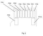
- Fig. 2 is a schematic view of the layout of the terminals (contacts) of the device for processing and storing data according to the embodiment of the present invention.
- the 8 contacts PIN1 to PIN 8 are arranged in a row, while the first additional port (PIN9) and the second additional port (PIN10) are arranged in another row.
- Table 1 PIN number Name Type Function description 1 DAT2 I/O Data line [Bit 2] 2 CD/DAT3 I/O Card surveillance/data line [Bit 3] 3 CMD P Command/response 4 VCC P Powering voltage 5 CLK I clock 6 VSS G ground 7 DAT0 I/O Data line [Bit 0] 8 DAT1 I/O Data line [Bit 1] 9 SWPIO I/O SWP data line 10 VCCSWP P Powering voltage from CLF
- the basic operating principle of the device for processing and storing data as disclosed herein is as follows:
- the client application When the SD card is used for remote payment, the client application will access the security element (SE) in the SD card via the 8 traditional contacts PIN1-8 defined in the original secure digital (SD) card interface protocol; while during the NFC payment in the field, the security element (SE) communicates with the NFC controller chip (such as a contactless frontend CLF) in the mobile terminal directly via PIN9 based on the SWP protocol, and then the NFC controller chip performs protocol transformation operation(i.e., the SWP protocol will be converted into the contactless communication protocol), and thus it can interact with the receiving terminal to implement the transaction function.
- the NFC controller chip such as a contactless frontend CLF
- the mobile terminal when the device for processing and storing data as disclosed herein is used in a mobile terminal, the following functionalities can also be performed by the mobile terminal:
- the mobile terminal When the device for processing and storing data as disclosed herein is inserted into the mobile terminal, the mobile terminal need not to be powered on for the security element (SE) to work properly so as to implement the NFC-based transaction function.
- SE security element
- the present invention is also intended to encompass a mobile terminal including the device for processing and storing data described above.
Landscapes
- Engineering & Computer Science (AREA)
- Physics & Mathematics (AREA)
- Theoretical Computer Science (AREA)
- General Physics & Mathematics (AREA)
- Computer Hardware Design (AREA)
- Toxicology (AREA)
- Microelectronics & Electronic Packaging (AREA)
- Health & Medical Sciences (AREA)
- Electromagnetism (AREA)
- General Health & Medical Sciences (AREA)
- Computer Vision & Pattern Recognition (AREA)
- Artificial Intelligence (AREA)
- Computer Security & Cryptography (AREA)
- Computing Systems (AREA)
- General Engineering & Computer Science (AREA)
- Computer Networks & Wireless Communication (AREA)
- Signal Processing (AREA)
- Storage Device Security (AREA)
- Telephone Function (AREA)
- Techniques For Improving Reliability Of Storages (AREA)
Abstract
Description
- This application is a translation of the international application
PCT/CN2012/078460 filed on July 11, 2012 201110196045.7, filed on July 13, 2011 - The present invention relates to a device for processing and storing data, and particularly, to a device for processing and storing data that supports single wire protocol.
- Nowadays, with the rapid development and popularization of the near-field communication (NFC) technology and the increasing enrichment of the business applications in different field, such as the financial transaction field, the mobile payment solutions based on the NFC technology become more and more important.
- In general, existing mobile payment solutions can be divided into the following two types: (1) a SIM card-based NFC solution, in which a contactless antenna and a contactless communication frontend (CLF) are integrated in a mobile phone, while a security element (SE) is integrated in a SIM card, which communicates with the contactless antenna and the CLF via a particular communication protocol, e.g., the single wire protocol; and (2) an SD card-based remote mobile payment solution, in which a security element (SE) is integrated in a SD card, and the access to the security element is made by using a particular client application to call a file interface of a standard SD card, and thereby the remote mobile payment process is implemented.
- However, the first solution described above is disadvantageous in that it does not support concurrent processing due to the small storage capacity of the existing SIM cards, which is usually 80 to 100kB, and this makes it difficult to extend the applications of NFC-based mobile payment in various business categories.
- The second solution described above is also disadvantageous for the following reasons: NFC-based mobile payment application may not be supported because a particular client application is required to access to the security element (SE) so as to call a file interface of a standard SD card; because the security element (SE) and the primary processor (i.e., the SDC) and the primary memory (i.e., a FLASH memory) in the SD card share the powering of the SD card interface, the powering of the security element (SE) may be insufficient or inversely effected such that it cannot work properly; because the access to the security element (SE) requires the calling of the file interface of the SD card, the external device will not be able to access the security element (SE) during the writing or reading process of the SD card, and thus this will limit the time for transaction.
- Therefore, there exists the need for a device for processing and storing data that supports the single wire protocol and a mobile terminal that includes such device for processing and storing data.
- In order to solve aforementioned problems of the existing solutions, a device for processing and storing data is disclosed in the present application.
- One of the objects of the present invention is implemented by the following technical solution:
- A device for processing and storing data, the device comprises a primary controller, a primary memory, a security element (SE), and at least one universal port, wherein based on a first communication protocol, the primary controller controls the primary memory and/or the security element (SE) to interact with a first external device via the at least one universal port so as to complete the processing and access of the data;
- characterized in that, the device for processing and storing data further includes a first additional port, via which the security element (SE) interacts with a second external device based on a second communication protocol to complete the processing and access of the data.
- In the solutions as disclosed above, preferably, the device for processing and storing data further includes a second additional port, via which the security element (SE) is powered.
- In the solutions as disclosed above, preferably, the second communication protocol is the single wire protocol (SWP).
- In the solutions as disclosed above, preferably, the first communication protocol is the secure digital (SD) card interface protocol.
- In the solutions as disclosed above, preferably, the at least one universal ports are 8 contacts PIN1-8 defined in the security digital (SD) card interface protocol.
- In the solutions as disclosed above, preferably, the first external device is a baseband chip in a mobile device.
- In the solutions as disclosed above, preferably, the second external device is a near-field communication (NFC) controller chip.
- In the solutions as disclosed above, preferably, the security element (SE) is used to process and store security information data, and wherein the processing includes data-based operations.
- In the solutions disclosed above, preferably, the primary memory is a FLASH memory.
- In the solutions as disclosed above, preferably, the device for processing and storing data has a shape of a normal SD card.
- In the solutions as disclosed above, preferably, the 8 contacts PIN1-8 are arranged in a row, while the first additional port and the second additional port are arranged in another row.
- The objects of the present invention can also be implemented by the following technical solutions:
- A mobile terminal including the device for processing and storing data as described above.
- The device for processing and storing data has the following advantages: (1) the security element (SE) can work independently without being effected by the data read/write process which is being performed in the primary memory; (2) the single wire protocol (SWP) is supported, and thus the security element (SE) can directly communication with a near-field communication (NFC) controller chip; and (3) the capacity of the primary memory and the security element (SE) is relatively large, and thus allowing for expanding mobile payment applications of various categories that are based-on the NFC technology.
- The features and advantages of the present invention will be better understood by one skilled in the art in connection with the drawings, in which:
-
Fig. 1 is a schematic view of the structure of the device for processing and storing data according to the embodiment of the present invention; and -
Fig. 2 is a schematic view of the layout of the terminals (contacts) of the device for processing and storing data according to the embodiment of the present invention. -
Fig. 1 is a schematic view of the structure of the device for processing and storing data according to the embodiment of the present invention. As shown inFig. 1 , the device for processing and storing data as disclosed herein includes aprimary controller 1, aprimary memory 2, a security element (SE) 3, and at least one universal ports (PIN1-8). Theprimary controller 1 controls theprimary memory 2 and/or the security element (SE) 3 based on a first communication protocol to interact with a first external device via the at least one universal port so as to complete the processing and access of the data. Moreover, the device for processing and storing data further includes a first additional port (PIN9), via which the security element (SE) 3 interacts with a second external device based on a second communication protocol to complete the processing and access of the data. - Preferably, in the device for processing and storing data as disclosed herein, the device for processing and storing data further includes a second additional port (PIN10), via which the security element (SE) 3 is powered. As an example, the powering voltage of the second additional port (PIN10) is from a near-field communication (NFC) controller chip, for example, a contactless frontend CLF.
- Preferably, in the device for processing and storing data as disclosed herein, the second communication protocol is the single wire protocol (SWP).
- Preferably, in the device for processing and storing data as disclosed herein, the first communication protocol is the secure digital (SD) card interface protocol.
- As an example, in the device for processing and storing data as disclosed herein, the at least one universal ports are 8 contacts PIN1-8 defined in the security digital (SD) card interface protocol.
- As an example, in the device for processing and storing data as disclosed herein, the first external device is a baseband chip in a mobile device.
- As an example, in the device for processing and storing data as disclosed herein, the second external device is a near-field communication (NFC) controller chip, such as a contactless frontend CLF.
- As an example, in the device for processing and storing data as disclosed herein, the security element (SE) 3 is used to process and store security information data, such as the data used for authenticating financial transactions. The processing mentioned above includes data-based operations, such as encryption and decryption operations.
- As an example, in the device for processing and storing data as disclosed herein, the
primary memory 2 is a FLASH memory. - As an example, as shown in
Fig. 1 , in the device for processing and storing data as disclosed herein, the device for processing and storing data has a shape of a normal SD card. -
Fig. 2 is a schematic view of the layout of the terminals (contacts) of the device for processing and storing data according to the embodiment of the present invention. As shown inFig. 2 , in the device for processing and storing data as disclosed herein, the 8 contacts PIN1 to PIN 8 are arranged in a row, while the first additional port (PIN9) and the second additional port (PIN10) are arranged in another row. - As an example, the definitions of the contacts PIN1-10 are shown in Table 1.
Table 1 PIN number Name Type Function description 1 DAT2 I/O Data line [Bit 2] 2 CD/DAT3 I/O Card surveillance/data line [Bit 3] 3 CMD P Command/response 4 VCC P Powering voltage 5 CLK I clock 6 VSS G ground 7 DAT0 I/O Data line [Bit 0] 8 DAT1 I/O Data line [Bit 1] 9 SWPIO I/O SWP data line 10 VCCSWP P Powering voltage from CLF - As an example, the basic operating principle of the device for processing and storing data as disclosed herein is as follows:
- The
primary controller 1 controls the primary memory 2 (e.g., the FLASH memory) and/or the security element (SE) 3 based on a first communication protocol (e.g., the secure digital (SD) card interface protocol) to interact with a first external device (e.g., a baseband chip of a mobile terminal) via the at least one universal port (PIN1-8) so as to complete the processing and access of the data; the security element (SE) 3 interacts with a second external device (e.g., a contactless frontend CLF) via a first additional port (PIN9) based on a second communication protocol (e.g., the SWP protocol) to complete the processing and access of the data, wherein the security element (SE) 3 is powered via a second additional port (PIN10). As can be seen, in the device for processing and storing data as disclosed herein, for example, the security element (SE) implements the single wire protocol (SWP) via a contact PIN9, and can be individually powered separately from the original powering system of the SD card via contact PIN10. Hence, the security element (SE) can work independently without being effected by the condition whether the data is being written into/read from the SD card. - As an example, in the mobile payment field, when the device for processing and storing data as disclosed herein is used in a mobile terminal, the following functionalities can be performed by the mobile terminal: When the SD card is used for remote payment, the client application will access the security element (SE) in the SD card via the 8 traditional contacts PIN1-8 defined in the original secure digital (SD) card interface protocol; while during the NFC payment in the field, the security element (SE) communicates with the NFC controller chip (such as a contactless frontend CLF) in the mobile terminal directly via PIN9 based on the SWP protocol, and then the NFC controller chip performs protocol transformation operation(i.e., the SWP protocol will be converted into the contactless communication protocol), and thus it can interact with the receiving terminal to implement the transaction function.
- As an example, in the mobile payment field, when the device for processing and storing data as disclosed herein is used in a mobile terminal, the following functionalities can also be performed by the mobile terminal: When the device for processing and storing data as disclosed herein is inserted into the mobile terminal, the mobile terminal need not to be powered on for the security element (SE) to work properly so as to implement the NFC-based transaction function.
- Moreover, the present invention is also intended to encompass a mobile terminal including the device for processing and storing data described above.
- Although the present invention has been described with the above preferred embodiments, the implementation of the invention is not limited to these embodiments. It should be appreciated that various changes and modifications may be made to the present invention by one skilled in the art without departing from the spirit and scope of the present invention.
Claims (12)
- A device for processing and storing data, the device comprises a primary controller, a primary memory, a security element (SE), and at least one universal port, wherein based on a first communication protocol, the primary controller controls the primary memory and/or the security element (SE) to interact with a first external device via the at least one universal port so as to complete the processing and access of the data; characterized in that, the device for processing and storing data further includes a first additional port, via which the security element (SE) interacts with a second external device based on a second communication protocol to complete the processing and access of the data.
- The device for processing and storing data of claim 1, characterized in that, the device for processing and storing data further includes a second additional port, via which the security element (SE) is powered.
- The device for processing and storing data of claim 2, characterized in that, the second communication protocol is the single wire protocol (SWP).
- The device for processing and storing data of claim 3, characterized in that, the first communication protocol is the secure digital (SD) card interface protocol.
- The device for processing and storing data of claim 4, characterized in that, the at least one universal ports are 8 contacts PIN1 to PIN 8 defined in the security digital (SD) card interface protocol.
- The device for processing and storing data of claim 5, characterized in that, the first external device is a baseband chip in a mobile device.
- The device for processing and storing data of claim 6, characterized in that, the second external device is a near-field communication (NFC) controller chip.
- The device for processing and storing data of claim 7, characterized in that, the security element (SE) is used to process and store the security information data, and wherein the processing includes data-based operations.
- The device for processing and storing data of claim 8, characterized in that, the primary memory is a FLASH memory.
- The device for processing and storing data of claim 9, characterized in that, the device for processing and storing data has a shape of a normal SD card.
- The device for processing and storing data of claim 10, characterized in that, the 8 contacts PIN1 to PIN8 are arranged in a row, while the first additional port and the second additional port are arranged in another row.
- A mobile terminal including the device for processing and storing data according to any of claims 1 to 11.
Applications Claiming Priority (2)
| Application Number | Priority Date | Filing Date | Title |
|---|---|---|---|
| CN201110196045.7A CN102880958B (en) | 2011-07-13 | 2011-07-13 | Data process and storage device |
| PCT/CN2012/078460 WO2013007189A1 (en) | 2011-07-13 | 2012-07-11 | Data processing and storage device |
Publications (3)
| Publication Number | Publication Date |
|---|---|
| EP2733645A1 true EP2733645A1 (en) | 2014-05-21 |
| EP2733645A4 EP2733645A4 (en) | 2015-02-18 |
| EP2733645B1 EP2733645B1 (en) | 2016-01-20 |
Family
ID=47482273
Family Applications (1)
| Application Number | Title | Priority Date | Filing Date |
|---|---|---|---|
| EP12810687.9A Active EP2733645B1 (en) | 2011-07-13 | 2012-07-11 | Data processing and storage device |
Country Status (6)
| Country | Link |
|---|---|
| US (1) | US9237157B2 (en) |
| EP (1) | EP2733645B1 (en) |
| CN (1) | CN102880958B (en) |
| ES (1) | ES2562657T3 (en) |
| TW (2) | TW201308227A (en) |
| WO (1) | WO2013007189A1 (en) |
Families Citing this family (3)
| Publication number | Priority date | Publication date | Assignee | Title |
|---|---|---|---|---|
| CN103559523B (en) * | 2013-11-15 | 2016-04-13 | 武汉天喻信息产业股份有限公司 | The contactless read-write device realized based on SWP SE and method |
| CN106101989A (en) * | 2016-06-22 | 2016-11-09 | 依偎科技(南昌)有限公司 | A kind of method selecting safe unit and mobile terminal |
| KR102783592B1 (en) | 2020-01-07 | 2025-03-19 | 삼성전자주식회사 | Card type solid state drive |
Family Cites Families (22)
| Publication number | Priority date | Publication date | Assignee | Title |
|---|---|---|---|---|
| US7762470B2 (en) * | 2003-11-17 | 2010-07-27 | Dpd Patent Trust Ltd. | RFID token with multiple interface controller |
| DE10355643B4 (en) * | 2003-11-28 | 2006-04-20 | Infineon Technologies Ag | Mobile station for processing GSM and TD-SCDMA radio standard signals |
| KR100596410B1 (en) * | 2004-11-04 | 2006-07-03 | 한국전자통신연구원 | SD Memory Card for Function Expansion |
| JP2006172121A (en) * | 2004-12-15 | 2006-06-29 | Toshiba Corp | Card-like storage device and its adapter and host device |
| WO2007012909A1 (en) * | 2005-07-25 | 2007-02-01 | Nokia Corporation | Method and device for operating a multifunctional near-field communication device supporting several data formats |
| US20070145152A1 (en) * | 2005-12-28 | 2007-06-28 | Fabrice Jogand-Coulomb | Nested memory system with near field communications capability |
| FR2898001A1 (en) * | 2006-02-28 | 2007-08-31 | Gemplus Sa | Secured digital content`s e.g. musical piece, secured access management method, involves producing file based on adapted access right, key and certificate, where file is accessible by terminal so that officer processes content based on file |
| GB2444798B (en) * | 2006-12-15 | 2010-06-30 | Innovision Res & Tech Plc | Communications devices comprising near field RF communicators |
| FR2913550A1 (en) * | 2007-03-07 | 2008-09-12 | Inside Contactless Sa | METHOD FOR SECURELY LOADING ACCESS DATA TO A SERVICE IN AN NFC CHIPSET |
| US7961101B2 (en) * | 2008-08-08 | 2011-06-14 | Tyfone, Inc. | Small RFID card with integrated inductive element |
| EP2161680A1 (en) * | 2008-09-08 | 2010-03-10 | Axalto S.A. | Device of SD ® type using a single wire protocol |
| SK288747B6 (en) * | 2009-04-24 | 2020-04-02 | Smk Kk | Method and system for cashless payment transactions, particularly with contactless payment device using |
| CN101789152B (en) * | 2010-02-11 | 2012-04-11 | 黄志军 | Multipurpose contactless card supporting large amount payment and online recharge and application method thereof |
| CN201638250U (en) * | 2010-03-25 | 2010-11-17 | 北京银达润和科技发展有限公司 | SD interface smart card capable of realizing cell phone payment |
| CN201766639U (en) * | 2010-05-28 | 2011-03-16 | 中兴通讯股份有限公司 | Mobile phone terminal |
| CN101937520B (en) * | 2010-09-03 | 2012-10-10 | 武汉天喻信息产业股份有限公司 | Telecom smart card for realizing near field communication function |
| CN102279940A (en) * | 2011-04-06 | 2011-12-14 | 武汉天喻信息产业股份有限公司 | SD card for mobile payment on the basis of SWP protocol |
| CN202351915U (en) * | 2011-04-18 | 2012-07-25 | 武汉天喻信息产业股份有限公司 | Mobile payment SD (Secure Digital) card based on SWP (Single Wire Protocol) |
| CN202075746U (en) * | 2011-04-26 | 2011-12-14 | 武汉天喻信息产业股份有限公司 | Reading equipment supporting mobile payment secure digital (SD) card based on single wire protocol (SWP) |
| CN102163273A (en) * | 2011-04-26 | 2011-08-24 | 武汉天喻信息产业股份有限公司 | Card reading equipment supporting SW-protocol-based mobile payment SD card |
| CN102325203B (en) * | 2011-05-10 | 2015-06-17 | 惠州Tcl移动通信有限公司 | Mobile terminal and communication device thereof |
| CN202306637U (en) * | 2011-07-13 | 2012-07-04 | 中国银联股份有限公司 | Data processing and storing device and mobile terminal containing same |
-
2011
- 2011-07-13 CN CN201110196045.7A patent/CN102880958B/en active Active
-
2012
- 2012-07-11 ES ES12810687.9T patent/ES2562657T3/en active Active
- 2012-07-11 EP EP12810687.9A patent/EP2733645B1/en active Active
- 2012-07-11 WO PCT/CN2012/078460 patent/WO2013007189A1/en not_active Ceased
- 2012-07-11 US US14/127,467 patent/US9237157B2/en active Active
- 2012-07-12 TW TW101125099A patent/TW201308227A/en unknown
- 2012-07-12 TW TW101224417U patent/TWM462913U/en not_active IP Right Cessation
Also Published As
| Publication number | Publication date |
|---|---|
| ES2562657T3 (en) | 2016-03-07 |
| WO2013007189A1 (en) | 2013-01-17 |
| EP2733645B1 (en) | 2016-01-20 |
| EP2733645A4 (en) | 2015-02-18 |
| TW201308227A (en) | 2013-02-16 |
| CN102880958B (en) | 2016-08-10 |
| US9237157B2 (en) | 2016-01-12 |
| CN102880958A (en) | 2013-01-16 |
| TWM462913U (en) | 2013-10-01 |
| US20140223517A1 (en) | 2014-08-07 |
Similar Documents
| Publication | Publication Date | Title |
|---|---|---|
| US9420409B2 (en) | Near field communication device | |
| EP2192523B1 (en) | Smart sd card and method of accessing the same | |
| TWI380219B (en) | Card reader with near field communication functions and near field communication device thereof | |
| US7757958B2 (en) | Card-shaped memory device incorporating IC card function, adapter for the same and host device | |
| US9741027B2 (en) | Memory card based contactless devices | |
| CN201408549Y (en) | U flash drive and smart card combined equipment | |
| EP2733645B1 (en) | Data processing and storage device | |
| CN101216899B (en) | SIM card chip compatible with non-contact logic encryption card | |
| JP2005293444A (en) | Memory card adapter and memory card | |
| CN102163273A (en) | Card reading equipment supporting SW-protocol-based mobile payment SD card | |
| TWM482145U (en) | Memory card with smart chip | |
| CN103886364B (en) | Memory card with intelligent chip | |
| CN101840486B (en) | Improved converter for SD card | |
| KR20190075284A (en) | Add-on SIM card for mobile communication device with it | |
| CN202306637U (en) | Data processing and storing device and mobile terminal containing same | |
| CN111918277B (en) | Data storage management | |
| WO2012079429A1 (en) | Storage device and configuration method thereof | |
| CN206431661U (en) | A kind of smart card and terminal device | |
| US20130290602A1 (en) | Data storage device | |
| KR200342943Y1 (en) | Dummy Terminal for Reading Smart Card | |
| CN115840968A (en) | Chip with logic encryption card and CPU card and communication method thereof | |
| CN103064643A (en) | Method of showing information on non-contact type integrated circuit (IC) card | |
| KR20070018228A (en) | Controller, Integrated circuit card having the controller, and Data processing method of the integrated circuit card | |
| TWM482222U (en) | Antenna structure with dual sensing extrapolation card and memory card |
Legal Events
| Date | Code | Title | Description |
|---|---|---|---|
| PUAI | Public reference made under article 153(3) epc to a published international application that has entered the european phase |
Free format text: ORIGINAL CODE: 0009012 |
|
| 17P | Request for examination filed |
Effective date: 20140109 |
|
| AK | Designated contracting states |
Kind code of ref document: A1 Designated state(s): AL AT BE BG CH CY CZ DE DK EE ES FI FR GB GR HR HU IE IS IT LI LT LU LV MC MK MT NL NO PL PT RO RS SE SI SK SM TR |
|
| DAX | Request for extension of the european patent (deleted) | ||
| A4 | Supplementary search report drawn up and despatched |
Effective date: 20150121 |
|
| RIC1 | Information provided on ipc code assigned before grant |
Ipc: G06K 19/077 20060101ALI20150115BHEP Ipc: G06K 7/10 20060101ALI20150115BHEP Ipc: G06K 19/07 20060101AFI20150115BHEP Ipc: H04L 29/06 20060101ALI20150115BHEP |
|
| GRAP | Despatch of communication of intention to grant a patent |
Free format text: ORIGINAL CODE: EPIDOSNIGR1 |
|
| INTG | Intention to grant announced |
Effective date: 20151007 |
|
| GRAS | Grant fee paid |
Free format text: ORIGINAL CODE: EPIDOSNIGR3 |
|
| GRAA | (expected) grant |
Free format text: ORIGINAL CODE: 0009210 |
|
| AK | Designated contracting states |
Kind code of ref document: B1 Designated state(s): AL AT BE BG CH CY CZ DE DK EE ES FI FR GB GR HR HU IE IS IT LI LT LU LV MC MK MT NL NO PL PT RO RS SE SI SK SM TR |
|
| REG | Reference to a national code |
Ref country code: GB Ref legal event code: FG4D |
|
| REG | Reference to a national code |
Ref country code: CH Ref legal event code: EP |
|
| REG | Reference to a national code |
Ref country code: IE Ref legal event code: FG4D |
|
| REG | Reference to a national code |
Ref country code: AT Ref legal event code: REF Ref document number: 772038 Country of ref document: AT Kind code of ref document: T Effective date: 20160215 |
|
| REG | Reference to a national code |
Ref country code: DE Ref legal event code: R096 Ref document number: 602012014225 Country of ref document: DE |
|
| REG | Reference to a national code |
Ref country code: ES Ref legal event code: FG2A Ref document number: 2562657 Country of ref document: ES Kind code of ref document: T3 Effective date: 20160307 |
|
| REG | Reference to a national code |
Ref country code: NL Ref legal event code: FP |
|
| REG | Reference to a national code |
Ref country code: LT Ref legal event code: MG4D |
|
| REG | Reference to a national code |
Ref country code: AT Ref legal event code: MK05 Ref document number: 772038 Country of ref document: AT Kind code of ref document: T Effective date: 20160120 |
|
| PG25 | Lapsed in a contracting state [announced via postgrant information from national office to epo] |
Ref country code: HR Free format text: LAPSE BECAUSE OF FAILURE TO SUBMIT A TRANSLATION OF THE DESCRIPTION OR TO PAY THE FEE WITHIN THE PRESCRIBED TIME-LIMIT Effective date: 20160120 Ref country code: GR Free format text: LAPSE BECAUSE OF FAILURE TO SUBMIT A TRANSLATION OF THE DESCRIPTION OR TO PAY THE FEE WITHIN THE PRESCRIBED TIME-LIMIT Effective date: 20160421 Ref country code: NO Free format text: LAPSE BECAUSE OF FAILURE TO SUBMIT A TRANSLATION OF THE DESCRIPTION OR TO PAY THE FEE WITHIN THE PRESCRIBED TIME-LIMIT Effective date: 20160420 Ref country code: IT Free format text: LAPSE BECAUSE OF FAILURE TO SUBMIT A TRANSLATION OF THE DESCRIPTION OR TO PAY THE FEE WITHIN THE PRESCRIBED TIME-LIMIT Effective date: 20160120 Ref country code: FI Free format text: LAPSE BECAUSE OF FAILURE TO SUBMIT A TRANSLATION OF THE DESCRIPTION OR TO PAY THE FEE WITHIN THE PRESCRIBED TIME-LIMIT Effective date: 20160120 |
|
| REG | Reference to a national code |
Ref country code: FR Ref legal event code: PLFP Year of fee payment: 5 |
|
| PG25 | Lapsed in a contracting state [announced via postgrant information from national office to epo] |
Ref country code: PT Free format text: LAPSE BECAUSE OF FAILURE TO SUBMIT A TRANSLATION OF THE DESCRIPTION OR TO PAY THE FEE WITHIN THE PRESCRIBED TIME-LIMIT Effective date: 20160520 Ref country code: PL Free format text: LAPSE BECAUSE OF FAILURE TO SUBMIT A TRANSLATION OF THE DESCRIPTION OR TO PAY THE FEE WITHIN THE PRESCRIBED TIME-LIMIT Effective date: 20160120 Ref country code: SE Free format text: LAPSE BECAUSE OF FAILURE TO SUBMIT A TRANSLATION OF THE DESCRIPTION OR TO PAY THE FEE WITHIN THE PRESCRIBED TIME-LIMIT Effective date: 20160120 Ref country code: LT Free format text: LAPSE BECAUSE OF FAILURE TO SUBMIT A TRANSLATION OF THE DESCRIPTION OR TO PAY THE FEE WITHIN THE PRESCRIBED TIME-LIMIT Effective date: 20160120 Ref country code: IS Free format text: LAPSE BECAUSE OF FAILURE TO SUBMIT A TRANSLATION OF THE DESCRIPTION OR TO PAY THE FEE WITHIN THE PRESCRIBED TIME-LIMIT Effective date: 20160520 Ref country code: AT Free format text: LAPSE BECAUSE OF FAILURE TO SUBMIT A TRANSLATION OF THE DESCRIPTION OR TO PAY THE FEE WITHIN THE PRESCRIBED TIME-LIMIT Effective date: 20160120 Ref country code: RS Free format text: LAPSE BECAUSE OF FAILURE TO SUBMIT A TRANSLATION OF THE DESCRIPTION OR TO PAY THE FEE WITHIN THE PRESCRIBED TIME-LIMIT Effective date: 20160120 Ref country code: LV Free format text: LAPSE BECAUSE OF FAILURE TO SUBMIT A TRANSLATION OF THE DESCRIPTION OR TO PAY THE FEE WITHIN THE PRESCRIBED TIME-LIMIT Effective date: 20160120 |
|
| REG | Reference to a national code |
Ref country code: DE Ref legal event code: R097 Ref document number: 602012014225 Country of ref document: DE |
|
| PG25 | Lapsed in a contracting state [announced via postgrant information from national office to epo] |
Ref country code: DK Free format text: LAPSE BECAUSE OF FAILURE TO SUBMIT A TRANSLATION OF THE DESCRIPTION OR TO PAY THE FEE WITHIN THE PRESCRIBED TIME-LIMIT Effective date: 20160120 Ref country code: EE Free format text: LAPSE BECAUSE OF FAILURE TO SUBMIT A TRANSLATION OF THE DESCRIPTION OR TO PAY THE FEE WITHIN THE PRESCRIBED TIME-LIMIT Effective date: 20160120 |
|
| PLBE | No opposition filed within time limit |
Free format text: ORIGINAL CODE: 0009261 |
|
| STAA | Information on the status of an ep patent application or granted ep patent |
Free format text: STATUS: NO OPPOSITION FILED WITHIN TIME LIMIT |
|
| PG25 | Lapsed in a contracting state [announced via postgrant information from national office to epo] |
Ref country code: SK Free format text: LAPSE BECAUSE OF FAILURE TO SUBMIT A TRANSLATION OF THE DESCRIPTION OR TO PAY THE FEE WITHIN THE PRESCRIBED TIME-LIMIT Effective date: 20160120 Ref country code: RO Free format text: LAPSE BECAUSE OF FAILURE TO SUBMIT A TRANSLATION OF THE DESCRIPTION OR TO PAY THE FEE WITHIN THE PRESCRIBED TIME-LIMIT Effective date: 20160120 Ref country code: CZ Free format text: LAPSE BECAUSE OF FAILURE TO SUBMIT A TRANSLATION OF THE DESCRIPTION OR TO PAY THE FEE WITHIN THE PRESCRIBED TIME-LIMIT Effective date: 20160120 Ref country code: SM Free format text: LAPSE BECAUSE OF FAILURE TO SUBMIT A TRANSLATION OF THE DESCRIPTION OR TO PAY THE FEE WITHIN THE PRESCRIBED TIME-LIMIT Effective date: 20160120 |
|
| 26N | No opposition filed |
Effective date: 20161021 |
|
| PG25 | Lapsed in a contracting state [announced via postgrant information from national office to epo] |
Ref country code: BE Free format text: LAPSE BECAUSE OF FAILURE TO SUBMIT A TRANSLATION OF THE DESCRIPTION OR TO PAY THE FEE WITHIN THE PRESCRIBED TIME-LIMIT Effective date: 20160120 |
|
| PG25 | Lapsed in a contracting state [announced via postgrant information from national office to epo] |
Ref country code: SI Free format text: LAPSE BECAUSE OF FAILURE TO SUBMIT A TRANSLATION OF THE DESCRIPTION OR TO PAY THE FEE WITHIN THE PRESCRIBED TIME-LIMIT Effective date: 20160120 Ref country code: BG Free format text: LAPSE BECAUSE OF FAILURE TO SUBMIT A TRANSLATION OF THE DESCRIPTION OR TO PAY THE FEE WITHIN THE PRESCRIBED TIME-LIMIT Effective date: 20160420 |
|
| REG | Reference to a national code |
Ref country code: CH Ref legal event code: PL |
|
| PG25 | Lapsed in a contracting state [announced via postgrant information from national office to epo] |
Ref country code: MC Free format text: LAPSE BECAUSE OF FAILURE TO SUBMIT A TRANSLATION OF THE DESCRIPTION OR TO PAY THE FEE WITHIN THE PRESCRIBED TIME-LIMIT Effective date: 20160120 |
|
| PG25 | Lapsed in a contracting state [announced via postgrant information from national office to epo] |
Ref country code: CH Free format text: LAPSE BECAUSE OF NON-PAYMENT OF DUE FEES Effective date: 20160731 Ref country code: LI Free format text: LAPSE BECAUSE OF NON-PAYMENT OF DUE FEES Effective date: 20160731 |
|
| REG | Reference to a national code |
Ref country code: IE Ref legal event code: MM4A |
|
| REG | Reference to a national code |
Ref country code: FR Ref legal event code: PLFP Year of fee payment: 6 |
|
| PG25 | Lapsed in a contracting state [announced via postgrant information from national office to epo] |
Ref country code: IE Free format text: LAPSE BECAUSE OF NON-PAYMENT OF DUE FEES Effective date: 20160711 |
|
| PG25 | Lapsed in a contracting state [announced via postgrant information from national office to epo] |
Ref country code: LU Free format text: LAPSE BECAUSE OF NON-PAYMENT OF DUE FEES Effective date: 20160711 |
|
| PG25 | Lapsed in a contracting state [announced via postgrant information from national office to epo] |
Ref country code: HU Free format text: LAPSE BECAUSE OF FAILURE TO SUBMIT A TRANSLATION OF THE DESCRIPTION OR TO PAY THE FEE WITHIN THE PRESCRIBED TIME-LIMIT; INVALID AB INITIO Effective date: 20120711 Ref country code: CY Free format text: LAPSE BECAUSE OF FAILURE TO SUBMIT A TRANSLATION OF THE DESCRIPTION OR TO PAY THE FEE WITHIN THE PRESCRIBED TIME-LIMIT Effective date: 20160120 |
|
| REG | Reference to a national code |
Ref country code: FR Ref legal event code: PLFP Year of fee payment: 7 |
|
| PG25 | Lapsed in a contracting state [announced via postgrant information from national office to epo] |
Ref country code: MK Free format text: LAPSE BECAUSE OF FAILURE TO SUBMIT A TRANSLATION OF THE DESCRIPTION OR TO PAY THE FEE WITHIN THE PRESCRIBED TIME-LIMIT Effective date: 20160120 Ref country code: MT Free format text: LAPSE BECAUSE OF NON-PAYMENT OF DUE FEES Effective date: 20160731 |
|
| PG25 | Lapsed in a contracting state [announced via postgrant information from national office to epo] |
Ref country code: AL Free format text: LAPSE BECAUSE OF FAILURE TO SUBMIT A TRANSLATION OF THE DESCRIPTION OR TO PAY THE FEE WITHIN THE PRESCRIBED TIME-LIMIT Effective date: 20160120 Ref country code: TR Free format text: LAPSE BECAUSE OF FAILURE TO SUBMIT A TRANSLATION OF THE DESCRIPTION OR TO PAY THE FEE WITHIN THE PRESCRIBED TIME-LIMIT Effective date: 20160120 |
|
| PGFP | Annual fee paid to national office [announced via postgrant information from national office to epo] |
Ref country code: NL Payment date: 20250526 Year of fee payment: 14 |
|
| PGFP | Annual fee paid to national office [announced via postgrant information from national office to epo] |
Ref country code: GB Payment date: 20250522 Year of fee payment: 14 |
|
| PGFP | Annual fee paid to national office [announced via postgrant information from national office to epo] |
Ref country code: FR Payment date: 20250523 Year of fee payment: 14 |
|
| PGFP | Annual fee paid to national office [announced via postgrant information from national office to epo] |
Ref country code: ES Payment date: 20250806 Year of fee payment: 14 |
|
| PGFP | Annual fee paid to national office [announced via postgrant information from national office to epo] |
Ref country code: DE Payment date: 20250521 Year of fee payment: 14 |