EP2733461B1 - Amplitude control for vibrating resonant sensors - Google Patents
Amplitude control for vibrating resonant sensors Download PDFInfo
- Publication number
- EP2733461B1 EP2733461B1 EP13191755.1A EP13191755A EP2733461B1 EP 2733461 B1 EP2733461 B1 EP 2733461B1 EP 13191755 A EP13191755 A EP 13191755A EP 2733461 B1 EP2733461 B1 EP 2733461B1
- Authority
- EP
- European Patent Office
- Prior art keywords
- signal
- resonator
- controller
- drive
- amplitude
- Prior art date
- Legal status (The legal status is an assumption and is not a legal conclusion. Google has not performed a legal analysis and makes no representation as to the accuracy of the status listed.)
- Active
Links
- 239000003990 capacitor Substances 0.000 claims description 29
- 230000010354 integration Effects 0.000 claims description 15
- 238000000034 method Methods 0.000 claims description 13
- 238000010586 diagram Methods 0.000 description 6
- 239000000284 extract Substances 0.000 description 4
- 230000005284 excitation Effects 0.000 description 3
- 230000008901 benefit Effects 0.000 description 2
- 238000006073 displacement reaction Methods 0.000 description 2
- 230000001133 acceleration Effects 0.000 description 1
- 230000001419 dependent effect Effects 0.000 description 1
- 230000000694 effects Effects 0.000 description 1
- 230000000116 mitigating effect Effects 0.000 description 1
- 230000010355 oscillation Effects 0.000 description 1
- 230000003071 parasitic effect Effects 0.000 description 1
- 230000035945 sensitivity Effects 0.000 description 1
Images
Classifications
-
- G—PHYSICS
- G01—MEASURING; TESTING
- G01H—MEASUREMENT OF MECHANICAL VIBRATIONS OR ULTRASONIC, SONIC OR INFRASONIC WAVES
- G01H3/00—Measuring characteristics of vibrations by using a detector in a fluid
-
- G—PHYSICS
- G01—MEASURING; TESTING
- G01C—MEASURING DISTANCES, LEVELS OR BEARINGS; SURVEYING; NAVIGATION; GYROSCOPIC INSTRUMENTS; PHOTOGRAMMETRY OR VIDEOGRAMMETRY
- G01C19/00—Gyroscopes; Turn-sensitive devices using vibrating masses; Turn-sensitive devices without moving masses; Measuring angular rate using gyroscopic effects
- G01C19/56—Turn-sensitive devices using vibrating masses, e.g. vibratory angular rate sensors based on Coriolis forces
- G01C19/5776—Signal processing not specific to any of the devices covered by groups G01C19/5607 - G01C19/5719
Definitions
- the present invention relates generally to inertial sensors, and more particularly to amplitude control for driving vibrating resonant sensors.
- Coriolis Vibratory Gyroscopes are useful for measuring or detecting angular movement or acceleration and are based on vibrating mechanical elements which sense rotation.
- a resonator of a CVG is excited into vibration at its resonant frequency. The direction or orientation of vibration is somewhat dependent on rotation of the sensor so that the vibration can be analyzed to sense directional changes.
- An amplitude control loop is used to apply excitation energy to the resonator of the CVG and to sense the resulting vibration.
- a number of circuits are employed to excite the resonator to resonance and to produce an output indicative of rotational rate.
- an amplitude control loop includes a low impedance buffer that extracts the charge from one or more capacitive pickoffs of a vibratory gyroscope to measure the amplitude of the resonator vibration.
- the resonator vibration responds to the amplitude of a drive signal supplied to one or more forcer electrodes to induce vibration in the gyroscope resonator.
- Capacitive pickoffs may be used to measure the vibratory displacement of the resonator through the electrical charge they produce.
- the charge from the capacitive pickoff(s) is transferred to an integration capacitor (C F ) where the charge is converted to an output voltage.
- That output voltage is sampled and, for the anti-nodal channels, is used to measure the amplitude of the resonator vibration.
- a controller adjusts the drive amplitude to maintain the measured vibration amplitude at a predetermined value. Also, by measuring both in-phase and quadrature components of the anti-nodal signal, it is possible to determine frequency error (i.e. deviation between the excitation frequency and the resonant frequency). A controller can then use this information to correct the frequency and ensure the drive tracks the resonant frequency of the CVG.
- the output voltage from the integration capacitor (C F ) is demodulated and provided to a summer which summed in an amplitude reference signal to produce an error signal.
- the gyro scale factor (which depends on the sensor vibration amplitude) is highly sensitive to the integration capacitor in the low-Z buffer circuit. If the capacitor C F varies, then for a given vibratory displacement, the voltage generated by the buffer will vary in inverse proportion to C F . The controller only has access to the voltage, thus by maintaining constant voltage amplitude, the true vibratory amplitude will in fact vary proportionally with the value of C F . Since the scale factor of the gyro depends directly on the vibratory amplitude, the scale factor accuracy is impacted. Also, the value of C F is small and therefore susceptible to many parasitic effects.
- US 4 479 098 A discloses a drive circuit for driving an actuator/mass at its natural resonance and for maintaining the instantaneous output signal of the mass at a predetermined constant value over a wide range of dynamically changing resonant frequencies.
- Current sensing circuitry detects an instantanous current passing through the actuator/mass.
- a compensation circuit modifies the instantaneous sensed circuit signal to compensate for dynamically changing physical parameters of the actuator mass and for phase irregularities introduced into the sensed signal when the mass oscillates near its natural resonance.
- Automatic gain control circuitry alters the actuator drive signal to maintain amplitude of the mass oscillation at a predetermined constant value.
- a drive circuit performs the actual drive function in response to the feedback signal received from the automatic gain control and compensation circuitry.
- a system for controlling a drive signal to a resonator of an inertial system.
- the system comprises a controller that provides the drive signal to a forcer coupled to the resonator to excite the resonator into vibration at its resonant frequency.
- the system further comprises a buffer an operational amplifier that includes an input terminal coupled to an input node and an integration capacitor coupled between the input node and an output of the operational amplifier, wherein the input node receives charge of a pickoff capacitor of the resonator that is a measure of the resonator vibration and a current reference waveform that are combined at the input node.
- the buffer provides an output that is a difference signal that represents an error of the resonator vibration that corresponds to a difference between the measured resonator vibration and the current reference waveform formed from a fixed amplitude reference signal, wherein the difference signal is demodulated and provided to the controller as a voltage that the controller attempts to drive to zero by adjusting the drive signal.
- a system for controlling a drive signal to a resonator of an inertial system.
- the system comprises a controller that provides the drive signal to a forcer coupled to the resonator to excite the resonator into vibration at its resonant frequency, and a buffer formed from an operational amplifier that includes an input terminal coupled to an input node and an integration capacitor coupled between the input node and an output of the operational amplifier, wherein the input node receives charge of a pickoff capacitor of the resonator that is a measure of the resonator vibration and a current reference waveform formed from a fixed amplitude reference signal, that are combined at the input node.
- the buffer provides an output that is a difference signal that represents an error of the resonator vibration that corresponds to a difference between the measured resonator vibration and the current reference waveform.
- the system further comprises a sine demodulator that demodulates a sine component of the difference signal and provides a low passed demodulated difference voltage to the controller, wherein the controller drives the low passed demodulated difference voltage to zero by adjusting a drive amplitude provided to a cosine modulator based on the output provided from the buffer wherein the drive amplitude and the cosine modulator that together provide the drive signal to the forcer.
- a method for controlling a drive signal to a resonator.
- the method comprises employing a drive signal to a forcer coupled to the resonator via a controller to excite the resonator into vibration at its resonant frequency, receiving charge of a pickoff capacitor of the resonator via a buffer, the charge being a measure of the resonator vibration, and combining a current reference waveform formed from a fixed amplitude reference signal with the received charge at an input node of the buffer to generate a difference signal.
- the difference signal represents an error of the resonator vibration that corresponds to a difference between the measured resonator vibration and the current reference waveform, demodulating the difference signal to generate a demodulated difference voltage to the controller, and adjusting an amplitude of the drive signal based on the demodulated difference voltage via the controller in order to null the demodulated difference voltage.
- the present invention provides for the injecting of a reference waveform into an input node of a low-impedance buffer that extracts the charge from a capacitive pickoff of a vibratory gyroscope to measure the amplitude of the resonator vibration.
- a resultant summed signal is transferred to an integration capacitor (C F ) of the low impedance buffer, whereby the summed signal is converted to an output voltage. That output voltage is sampled and, for the anti-nodal channels, is used to determine the amplitude error of the resonator vibration.
- the output voltage signal represents an error of the resonator vibration that corresponds to a difference between the measured resonator vibration and the current reference waveform.
- the output voltage signal is demodulated and low-pass filtered to generate a slowly varying signal corresponding to the amplitude of the output voltage at the excitation frequency.
- the demodulated and low-pass filtered output voltage represents the amplitude error of the vibration signal relative to the current reference waveform and can now be driven to NULL by a controller, instead of a predetermined amplitude reference as is conventional.
- the output voltage of the low impedance buffer is driven to null, it becomes completely insensitive to the precise value of the integration capacitor (C F ), thereby mitigating problems associated with the integration capacitor (C F ) stability.
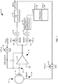
- FIG. 1 illustrates a functional block diagram of a system 10 for controlling a drive signal to a resonator 12 in accordance with an aspect of the present invention.
- the drive signal can be, for example, a drive amplitude signal.
- the system 10 includes a pickoff capacitor 14 formed from a wall of the resonator 12 and a capacitive pickoff electrode adjacent the wall of the resonator 12.
- a low-impedance buffer 20 extracts the charge from the capacitive pickoff electrode to measure the resonator vibration signal.
- the resonator vibration signal is responsive to a drive signal applied to a forcer electrode 16 to induce vibration at a resonator frequency of the resonator 12 of the vibratory gyroscope.
- a precision current reference waveform and the charge from the capacitive pickoff are combined at an input node 18 of an operational amplifier 22 of the low impedance buffer 20 and transferred to an integration capacitor (C F ) of the low impedance buffer 20, where the sum or difference of the charge of the pickoff capacitor 14 and precision current reference waveform is converted to an output voltage. That output voltage is sampled and, for the anti-nodal channels, is used to measure the amplitude error of the resonator vibration.
- the output voltage signal from the low impedance buffer 20 represents an error of the resonator vibration waveform as compared to the current reference waveform.
- the precision current reference waveform is formed from a fixed amplitude reference signal that is modulated by a modulator 24 operating at a drive frequency and based on a cosine reference signal (COS ⁇ t) to provide a modulated reference waveform having a pre-determined constant amplitude.
- the output of the modulator 24 is converted to a precision current reference waveform using a precision resistor (R). Since the modulator 24 and the resistor (R) are inherently much more stable than the integration capacitor (C F ), the precision current reference waveform is also very stable.
- the precision current reference waveform is injected into the input node 18 of the low impedance buffer 20.
- the output of the low impedance buffer 20 is demodulated and low-pass filtered into a voltage representative of the resonator vibration signal amplitude error that is driven to NULL by a proportional-integral-derivative (PID) controller 36 instead of to a predetermined amplitude reference as is conventional.
- PID proportional-integral-derivative
- a sine component of the error signal is demodulated by a demodulator 26 based on a sine reference signal (SIN ⁇ t) and provided to the PID controller 36 through a low pass filter 30.
- the PID controller 36 adjusts the drive amplitude signal to maintain the resonator vibration amplitude at a predetermined value based on the measured error signal.
- the drive amplitude signal is modulated by a modulator 42 based on the (COS ⁇ t) reference signal and provided to the forcer electrode 16 to drive the resonator vibration amplitude.
- a cosine component of the error signal of the low impedance buffer 20 is demodulated by a demodulator 32 based on the cosine reference signal (COS ⁇ t) and provided to a frequency correction controller 38, which provides a frequency adjustment to a frequency synthesizer 40 by driving the cosine demodulated signal to null to maintain the drive frequency at the resonant frequency of the resonator 12 as is known in the art for controlling resonant systems.
- the frequency synthesizer 40 generates the cosine reference signal (COS ⁇ t) and the sine reference signal (SIN ⁇ t).
- the vibratory amplitude in terms of current are matched to the precision reference current waveform. This ensures constant vibratory amplitude independent of the value of C F .
- C F affects the loop gain of the PID controller 36 but has no effect on the amplitude of the gyroscope, since C F is now operating on a NULL signal rather than a large amplitude signal.
- the resonator vibration signal will either match the reference signal, or will be 180 degrees out of phase with the reference signal. In either case, the amplitude of the resonator vibration signal will match the amplitude of the reference signal.
- An additional benefit of the FIG. 1 architecture is that it permits the gain of the low impedance buffer 20 to be higher (since it is operating at null), thus it should be possible to match the gains of the anti-nodal and nodal amplifiers
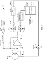
- FIG. 2 illustrates a functional block diagram of another system 50 for controlling a drive signal to a resonator 52 in accordance with an aspect of the present invention.
- the system 50 includes a pickoff capacitor 54 formed from a wall of the resonator and a capacitive pickoff electrode adjacent the wall of the resonator 52.
- a low-impedance buffer 60 extracts the charge from the capacitive pickoff electrode to measure the resonator vibration signal.
- the resonator vibration signal is responsive to a drive signal applied to a forcer electrode 56 to induce vibration in the resonator 52 of the vibratory gyroscope.
- a precision current square waveform and the charge from the capacitive pickoff are combined at an input node 58 of an operational amplifier 62 of the low impedance buffer 60 and transferred to an integration capacitor (C F ) of the low impedance buffer 60, where the sum or difference of the charge of the pickoff capacitor 54 and precision current square waveform is converted to an output voltage. That output voltage is sampled and, for the anti-nodal channels, is used to measure the amplitude error of the resonator vibration.
- the output voltage signal from the low impedance buffer 20 represents an error of the resonator vibration compared to the current reference waveform.
- the precision current square waveform is formed from an amplitude reference signal which is a precision square reference waveform with precision amplitude.
- the precision square reference waveform does not provide continuous instantaneous null operation, since the current from the sensor pickoffs will remain sinusoidal, but still preserves a null integrated value at the output of the low impedance buffer 60 over each cycle.
- the portions left over during cancellation due to the non-sinusoidal nature of the square waveform average to zero.
- this approach remains insensitive to the value of C F .
- a sine component of the error signal is demodulated by a demodulator 64 based on a sine reference signal (SIN ⁇ t) and provided to a PID controller 68 through a low pass filter 66.
- the PID controller 68 adjusts the drive amplitude signal to maintain the resonator vibration amplitude at a predetermined value based on the measured error signal.
- the drive amplitude signal is modulated by a modulator based on the cosine reference signal (COS ⁇ t) and provided to the forcer electrode 56 to drive the resonator vibration amplitude.
- a cosine component of the error signal is demodulated by a demodulator 70 based on the cosine reference signal (COS ⁇ t) and provided to a frequency correction controller 74, which provides a frequency adjustment to a frequency synthesizer 76 by driving the cosine demodulated signal to null to maintain the drive frequency at the resonant frequency of the resonator 52.
- the frequency synthesizer 76 generates the cosine reference signal (COS ⁇ t), the sine reference signal (SIN ⁇ t) and the precision square reference waveform at the same frequency.
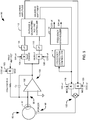
- FIG. 3 illustrates a functional block diagram of yet another system 90 for controlling a drive signal to a resonator 92 in accordance with an aspect of the present invention.
- the system 90 includes a pickoff capacitor 94, low impedance buffer 100, and a drive signal to a forcer electrode 96 to induce vibration in the resonator of the vibratory gyroscope.
- the system 90 also includes a precision current reference waveform formed from a fixed amplitude reference signal that is modulated by a modulator 103 operating at a drive frequency and based on a cosine reference signal (COS ⁇ t).
- COS ⁇ t cosine reference signal
- the precision current reference waveform is provided to an input node 98 of the low impedance buffer 100 that is an input of an operational amplifier 102 to mitigate stability issues associated with the integration capacitor (C F ).
- C F integration capacitor
- a precision current square waveform as illustrated in FIG. 2 , could be employed to mitigate issues associated with C F sensitivity.
- a sine component of the error signal of the low impedance buffer 100 is demodulated by a demodulator 104 based on a sine reference signal (SIN ⁇ t) and provided to an in-phase and quadrature nulling controller 112 through a low pass filter 106.
- a cosine component of the error signal of the low impedance buffer is demodulated by a demodulator 108 based on the cosine reference signal (COS ⁇ t) and provided to the in-phase and quadrature nulling controller 112 through a low pass filter 110.
- the in-phase and quadrature nulling controller 112 is used to drive the resonator with both a sine and a cosine phase to achieve a vibratory signal matching the fixed amplitude reference signal.
- a frequency correction controller 114 adjusts the frequency provided to a frequency synthesizer 116 ultimately to keep the sine phase drive minimized.
- the frequency synthesizer 116 generates the cosine reference signal (COS ⁇ t), and the sine reference signal (SIN ⁇ t).
- the cosine drive amplitude is modulated by a modulator 120 based on the cosine reference signal (COS ⁇ t) and the sine drive amplitude is modulated by a modulator 118 based on the sine reference signal (SIN ⁇ t).
- the modulated cosine and sine drive amplitude signals are combined by a combiner 122 and provided to the forcer electrode 96 to drive the resonator vibration.
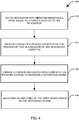
- FIG. 4 a methodology in accordance with various aspects of the present invention will be better appreciated with reference to FIG. 4 . While, for purposes of simplicity of explanation, the methodology of FIG. 4 is shown and described as executing serially, it is to be understood and appreciated that the present invention is not limited by the illustrated order, as some aspects could, in accordance with the present invention, occur in different orders and/or concurrently with other aspects from that shown and described.
- FIG. 4 illustrates a method 150 for controlling a drive signal to a resonator in accordance with an aspect of the present invention.
- the method begins at 152 where a resonator of a vibratory gyroscope is excited into vibration at its resonant frequency employing a drive signal to a forcer coupled to the resonator.
- charge of a pickoff capacitor is received that is a measure of the resonator vibration.
- a current reference waveform is combined with the received measured charge from the pickoff capacitor to generate a difference signal.
- an amplitude of the drive signal is adjusted based on the difference signal. The difference signal provides an error between the measured vibration signal and the current reference waveform.
- the difference signal is demodulated to generate an error signal which is a measure of the amplitude error.
- the error signal can now be driven to NULL by a controller to ensure the resonator vibration signal amplitude is maintained at the desired value, matching the current reference waveform amplitude.
- the current reference waveform can be provided from a fixed amplitude reference signal that is cosine modulated and provided through a precision resistor. Alternatively, the current reference waveform can be provided from a precision square wave through a precision resistor.
Description
- The present invention relates generally to inertial sensors, and more particularly to amplitude control for driving vibrating resonant sensors.
- Coriolis Vibratory Gyroscopes (CVGs) are useful for measuring or detecting angular movement or acceleration and are based on vibrating mechanical elements which sense rotation. A resonator of a CVG is excited into vibration at its resonant frequency. The direction or orientation of vibration is somewhat dependent on rotation of the sensor so that the vibration can be analyzed to sense directional changes. An amplitude control loop is used to apply excitation energy to the resonator of the CVG and to sense the resulting vibration. A number of circuits are employed to excite the resonator to resonance and to produce an output indicative of rotational rate.
- In certain CVGs, an amplitude control loop includes a low impedance buffer that extracts the charge from one or more capacitive pickoffs of a vibratory gyroscope to measure the amplitude of the resonator vibration. The resonator vibration responds to the amplitude of a drive signal supplied to one or more forcer electrodes to induce vibration in the gyroscope resonator. Capacitive pickoffs may be used to measure the vibratory displacement of the resonator through the electrical charge they produce. The charge from the capacitive pickoff(s) is transferred to an integration capacitor (CF) where the charge is converted to an output voltage. That output voltage is sampled and, for the anti-nodal channels, is used to measure the amplitude of the resonator vibration. A controller adjusts the drive amplitude to maintain the measured vibration amplitude at a predetermined value. Also, by measuring both in-phase and quadrature components of the anti-nodal signal, it is possible to determine frequency error (i.e. deviation between the excitation frequency and the resonant frequency). A controller can then use this information to correct the frequency and ensure the drive tracks the resonant frequency of the CVG.
- The output voltage from the integration capacitor (CF) is demodulated and provided to a summer which summed in an amplitude reference signal to produce an error signal. However, the gyro scale factor (which depends on the sensor vibration amplitude) is highly sensitive to the integration capacitor in the low-Z buffer circuit. If the capacitor CF varies, then for a given vibratory displacement, the voltage generated by the buffer will vary in inverse proportion to CF. The controller only has access to the voltage, thus by maintaining constant voltage amplitude, the true vibratory amplitude will in fact vary proportionally with the value of CF. Since the scale factor of the gyro depends directly on the vibratory amplitude, the scale factor accuracy is impacted. Also, the value of CF is small and therefore susceptible to many parasitic effects.
-
US 4 479 098 A discloses a drive circuit for driving an actuator/mass at its natural resonance and for maintaining the instantaneous output signal of the mass at a predetermined constant value over a wide range of dynamically changing resonant frequencies. Current sensing circuitry detects an instantanous current passing through the actuator/mass. A compensation circuit modifies the instantaneous sensed circuit signal to compensate for dynamically changing physical parameters of the actuator mass and for phase irregularities introduced into the sensed signal when the mass oscillates near its natural resonance. Automatic gain control circuitry alters the actuator drive signal to maintain amplitude of the mass oscillation at a predetermined constant value. A drive circuit performs the actual drive function in response to the feedback signal received from the automatic gain control and compensation circuitry. - In accordance with an aspect of the invention, a system is provided for controlling a drive signal to a resonator of an inertial system. The system comprises a controller that provides the drive signal to a forcer coupled to the resonator to excite the resonator into vibration at its resonant frequency. The system further comprises a buffer an operational amplifier that includes an input terminal coupled to an input node and an integration capacitor coupled between the input node and an output of the operational amplifier, wherein the input node receives charge of a pickoff capacitor of the resonator that is a measure of the resonator vibration and a current reference waveform that are combined at the input node. The buffer provides an output that is a difference signal that represents an error of the resonator vibration that corresponds to a difference between the measured resonator vibration and the current reference waveform formed from a fixed amplitude reference signal, wherein the difference signal is demodulated and provided to the controller as a voltage that the controller attempts to drive to zero by adjusting the drive signal.
- In accordance with another aspect of the invention, a system is provided for controlling a drive signal to a resonator of an inertial system. The system comprises a controller that provides the drive signal to a forcer coupled to the resonator to excite the resonator into vibration at its resonant frequency, and a buffer formed from an operational amplifier that includes an input terminal coupled to an input node and an integration capacitor coupled between the input node and an output of the operational amplifier, wherein the input node receives charge of a pickoff capacitor of the resonator that is a measure of the resonator vibration and a current reference waveform formed from a fixed amplitude reference signal, that are combined at the input node. The buffer provides an output that is a difference signal that represents an error of the resonator vibration that corresponds to a difference between the measured resonator vibration and the current reference waveform. The system further comprises a sine demodulator that demodulates a sine component of the difference signal and provides a low passed demodulated difference voltage to the controller, wherein the controller drives the low passed demodulated difference voltage to zero by adjusting a drive amplitude provided to a cosine modulator based on the output provided from the buffer wherein the drive amplitude and the cosine modulator that together provide the drive signal to the forcer.
- In accordance with yet another aspect of the current invention, a method is provided for controlling a drive signal to a resonator. The method comprises employing a drive signal to a forcer coupled to the resonator via a controller to excite the resonator into vibration at its resonant frequency, receiving charge of a pickoff capacitor of the resonator via a buffer, the charge being a measure of the resonator vibration, and combining a current reference waveform formed from a fixed amplitude reference signal with the received charge at an input node of the buffer to generate a difference signal. The difference signal represents an error of the resonator vibration that corresponds to a difference between the measured resonator vibration and the current reference waveform, demodulating the difference signal to generate a demodulated difference voltage to the controller, and adjusting an amplitude of the drive signal based on the demodulated difference voltage via the controller in order to null the demodulated difference voltage.
-
-
FIG. 1 illustrates a functional block diagram of a system for controlling a drive signal to a resonator in accordance with an aspect of the present invention. -
FIG. 2 illustrates a functional block diagram of another system for controlling a drive signal to a resonator in accordance with an aspect of the present invention. -
FIG. 3 illustrates a functional block diagram of yet another system for controlling a drive signal to a resonator in accordance with an aspect of the present invention. -
FIG. 4 illustrates a method for controlling a drive signal to a resonator in accordance with an aspect of the present invention. - The present invention provides for the injecting of a reference waveform into an input node of a low-impedance buffer that extracts the charge from a capacitive pickoff of a vibratory gyroscope to measure the amplitude of the resonator vibration. A resultant summed signal is transferred to an integration capacitor (CF) of the low impedance buffer, whereby the summed signal is converted to an output voltage. That output voltage is sampled and, for the anti-nodal channels, is used to determine the amplitude error of the resonator vibration. The output voltage signal represents an error of the resonator vibration that corresponds to a difference between the measured resonator vibration and the current reference waveform. The output voltage signal is demodulated and low-pass filtered to generate a slowly varying signal corresponding to the amplitude of the output voltage at the excitation frequency. The demodulated and low-pass filtered output voltage represents the amplitude error of the vibration signal relative to the current reference waveform and can now be driven to NULL by a controller, instead of a predetermined amplitude reference as is conventional. When the output voltage of the low impedance buffer is driven to null, it becomes completely insensitive to the precise value of the integration capacitor (CF), thereby mitigating problems associated with the integration capacitor (CF) stability.
-
FIG. 1 illustrates a functional block diagram of asystem 10 for controlling a drive signal to aresonator 12 in accordance with an aspect of the present invention. The drive signal can be, for example, a drive amplitude signal. Thesystem 10 includes apickoff capacitor 14 formed from a wall of theresonator 12 and a capacitive pickoff electrode adjacent the wall of theresonator 12. A low-impedance buffer 20 extracts the charge from the capacitive pickoff electrode to measure the resonator vibration signal. The resonator vibration signal is responsive to a drive signal applied to aforcer electrode 16 to induce vibration at a resonator frequency of theresonator 12 of the vibratory gyroscope. - A precision current reference waveform and the charge from the capacitive pickoff are combined at an
input node 18 of anoperational amplifier 22 of thelow impedance buffer 20 and transferred to an integration capacitor (CF) of thelow impedance buffer 20, where the sum or difference of the charge of thepickoff capacitor 14 and precision current reference waveform is converted to an output voltage. That output voltage is sampled and, for the anti-nodal channels, is used to measure the amplitude error of the resonator vibration. The output voltage signal from thelow impedance buffer 20 represents an error of the resonator vibration waveform as compared to the current reference waveform. - The precision current reference waveform is formed from a fixed amplitude reference signal that is modulated by a
modulator 24 operating at a drive frequency and based on a cosine reference signal (COS ωt) to provide a modulated reference waveform having a pre-determined constant amplitude. The output of themodulator 24 is converted to a precision current reference waveform using a precision resistor (R). Since themodulator 24 and the resistor (R) are inherently much more stable than the integration capacitor (CF), the precision current reference waveform is also very stable. The precision current reference waveform is injected into theinput node 18 of thelow impedance buffer 20. The output of thelow impedance buffer 20 is demodulated and low-pass filtered into a voltage representative of the resonator vibration signal amplitude error that is driven to NULL by a proportional-integral-derivative (PID)controller 36 instead of to a predetermined amplitude reference as is conventional. - A sine component of the error signal is demodulated by a
demodulator 26 based on a sine reference signal (SIN ωt) and provided to thePID controller 36 through alow pass filter 30. ThePID controller 36 adjusts the drive amplitude signal to maintain the resonator vibration amplitude at a predetermined value based on the measured error signal. The drive amplitude signal is modulated by amodulator 42 based on the (COS ωt) reference signal and provided to theforcer electrode 16 to drive the resonator vibration amplitude. A cosine component of the error signal of thelow impedance buffer 20 is demodulated by ademodulator 32 based on the cosine reference signal (COS ωt) and provided to afrequency correction controller 38, which provides a frequency adjustment to afrequency synthesizer 40 by driving the cosine demodulated signal to null to maintain the drive frequency at the resonant frequency of theresonator 12 as is known in the art for controlling resonant systems. Thefrequency synthesizer 40 generates the cosine reference signal (COS ωt) and the sine reference signal (SIN ωt). - In the example of
FIG. 1 , the vibratory amplitude in terms of current are matched to the precision reference current waveform. This ensures constant vibratory amplitude independent of the value of CF. In fact, in the architecture shown inFIG. 1 , CF affects the loop gain of thePID controller 36 but has no effect on the amplitude of the gyroscope, since CF is now operating on a NULL signal rather than a large amplitude signal. The null condition is achieved by the drive amplitude control loop which causes the resonator vibratory amplitude to match that of the fixed amplitude reference signal and by the frequency control loop which forces the phase of the vibratory signal to match that of the drive frequency (f of COS ωt where ω=2πf) (resonant condition). Under this null condition, depending on whether the current reference waveform is subtracted from or added to the resonator vibration signal, the resonator vibration signal will either match the reference signal, or will be 180 degrees out of phase with the reference signal. In either case, the amplitude of the resonator vibration signal will match the amplitude of the reference signal. An additional benefit of theFIG. 1 architecture is that it permits the gain of thelow impedance buffer 20 to be higher (since it is operating at null), thus it should be possible to match the gains of the anti-nodal and nodal amplifiers -
FIG. 2 illustrates a functional block diagram of anothersystem 50 for controlling a drive signal to aresonator 52 in accordance with an aspect of the present invention. Thesystem 50 includes apickoff capacitor 54 formed from a wall of the resonator and a capacitive pickoff electrode adjacent the wall of theresonator 52. A low-impedance buffer 60 extracts the charge from the capacitive pickoff electrode to measure the resonator vibration signal. The resonator vibration signal is responsive to a drive signal applied to aforcer electrode 56 to induce vibration in theresonator 52 of the vibratory gyroscope. - A precision current square waveform and the charge from the capacitive pickoff are combined at an
input node 58 of anoperational amplifier 62 of thelow impedance buffer 60 and transferred to an integration capacitor (CF) of thelow impedance buffer 60, where the sum or difference of the charge of thepickoff capacitor 54 and precision current square waveform is converted to an output voltage. That output voltage is sampled and, for the anti-nodal channels, is used to measure the amplitude error of the resonator vibration. The output voltage signal from thelow impedance buffer 20 represents an error of the resonator vibration compared to the current reference waveform. - The precision current square waveform is formed from an amplitude reference signal which is a precision square reference waveform with precision amplitude. In this case, the precision square reference waveform does not provide continuous instantaneous null operation, since the current from the sensor pickoffs will remain sinusoidal, but still preserves a null integrated value at the output of the
low impedance buffer 60 over each cycle. However, the portions left over during cancellation due to the non-sinusoidal nature of the square waveform average to zero. Thus, this approach remains insensitive to the value of CF. - A sine component of the error signal is demodulated by a
demodulator 64 based on a sine reference signal (SIN ωt) and provided to aPID controller 68 through a low pass filter 66. ThePID controller 68 adjusts the drive amplitude signal to maintain the resonator vibration amplitude at a predetermined value based on the measured error signal. The drive amplitude signal is modulated by a modulator based on the cosine reference signal (COS ωt) and provided to theforcer electrode 56 to drive the resonator vibration amplitude. A cosine component of the error signal is demodulated by ademodulator 70 based on the cosine reference signal (COS ωt) and provided to afrequency correction controller 74, which provides a frequency adjustment to a frequency synthesizer 76 by driving the cosine demodulated signal to null to maintain the drive frequency at the resonant frequency of theresonator 52. The frequency synthesizer 76 generates the cosine reference signal (COS ωt), the sine reference signal (SIN ωt) and the precision square reference waveform at the same frequency. -
FIG. 3 illustrates a functional block diagram of yet anothersystem 90 for controlling a drive signal to aresonator 92 in accordance with an aspect of the present invention. Similarly to thesystem 10 illustrated inFIG. 1 , thesystem 90 includes apickoff capacitor 94,low impedance buffer 100, and a drive signal to aforcer electrode 96 to induce vibration in the resonator of the vibratory gyroscope. Thesystem 90 also includes a precision current reference waveform formed from a fixed amplitude reference signal that is modulated by amodulator 103 operating at a drive frequency and based on a cosine reference signal (COS ωt). The precision current reference waveform is provided to aninput node 98 of thelow impedance buffer 100 that is an input of anoperational amplifier 102 to mitigate stability issues associated with the integration capacitor (CF). Alternatively, a precision current square waveform, as illustrated inFIG. 2 , could be employed to mitigate issues associated with CF sensitivity. - A sine component of the error signal of the
low impedance buffer 100 is demodulated by ademodulator 104 based on a sine reference signal (SIN ωt) and provided to an in-phase andquadrature nulling controller 112 through alow pass filter 106. A cosine component of the error signal of the low impedance buffer is demodulated by ademodulator 108 based on the cosine reference signal (COS ωt) and provided to the in-phase andquadrature nulling controller 112 through alow pass filter 110. The in-phase andquadrature nulling controller 112 is used to drive the resonator with both a sine and a cosine phase to achieve a vibratory signal matching the fixed amplitude reference signal. A controller of this type is described in commonly ownedU.S. Patent 4,981,351 , entitled "RING LASER GYROSCOPE DITHER DRIVE SYSTEM AND METHOD". The advantage of this approach, although more complex from a controls point of view, is that it affords greater bandwidth for controlling the resonator amplitude and better rejection of cross-coupled mechanical signals. - At resonance, the sine phase drive amplitude should be zero, thus the amplitude of the sine phase drive can be used to measure frequency error. A
frequency correction controller 114 adjusts the frequency provided to afrequency synthesizer 116 ultimately to keep the sine phase drive minimized. Thefrequency synthesizer 116 generates the cosine reference signal (COS ωt), and the sine reference signal (SIN ωt). The cosine drive amplitude is modulated by amodulator 120 based on the cosine reference signal (COS ωt) and the sine drive amplitude is modulated by amodulator 118 based on the sine reference signal (SIN ωt). The modulated cosine and sine drive amplitude signals are combined by acombiner 122 and provided to theforcer electrode 96 to drive the resonator vibration. - In view of the foregoing structural and functional features described above, a methodology in accordance with various aspects of the present invention will be better appreciated with reference to
FIG. 4 . While, for purposes of simplicity of explanation, the methodology ofFIG. 4 is shown and described as executing serially, it is to be understood and appreciated that the present invention is not limited by the illustrated order, as some aspects could, in accordance with the present invention, occur in different orders and/or concurrently with other aspects from that shown and described. -
FIG. 4 illustrates amethod 150 for controlling a drive signal to a resonator in accordance with an aspect of the present invention. The method begins at 152 where a resonator of a vibratory gyroscope is excited into vibration at its resonant frequency employing a drive signal to a forcer coupled to the resonator. At 154, charge of a pickoff capacitor is received that is a measure of the resonator vibration. At 156, a current reference waveform is combined with the received measured charge from the pickoff capacitor to generate a difference signal. At 158, an amplitude of the drive signal is adjusted based on the difference signal. The difference signal provides an error between the measured vibration signal and the current reference waveform. The difference signal is demodulated to generate an error signal which is a measure of the amplitude error. The error signal can now be driven to NULL by a controller to ensure the resonator vibration signal amplitude is maintained at the desired value, matching the current reference waveform amplitude. The current reference waveform can be provided from a fixed amplitude reference signal that is cosine modulated and provided through a precision resistor. Alternatively, the current reference waveform can be provided from a precision square wave through a precision resistor. - What have been described above are examples of the invention. One of ordinary skill in the art will recognize that many further combinations and permutations of the invention are possible. For example, COS ωt and SIN ωt may be interchanged depending on the specific details of the resonator and the configuration of the circuitry. In addition, while the above example description of the invention is provided for a vibratory gyro, it is understood that the invention could also apply to other vibratory sensors requiring amplitude control.
Claims (18)
- A system (10, 50, 90) for controlling a drive signal to a resonator (12, 52, 92) of an inertial system, the system (10, 50, 90) comprising:a controller (36, 68, 112) that provides the drive signal to a forcer coupled to the resonator (12, 52, 92) to excite the resonator (12, 52, 92) into vibration at its resonant frequency; anda buffer (20, 60, 100) formed from an operational amplifier that includes an input terminal coupled to an input node (18, 58, 98) and an integration capacitor coupled between the input node (18, 58, 98) and an output of the operational amplifier, wherein the input node (18, 58, 98) receives charge of a pickoff capacitor of the resonator (12, 52, 92) that is a measure of the resonator vibration and a current reference waveform that are combined at the input node (18, 58, 98) and provides an output that is a difference signal that represents an error of the resonator vibration that corresponds to a difference between the measured resonator vibration and the current reference waveform formed from a fixed amplitude reference signal, wherein the difference signal is demodulated and provided to the controller (36, 68, 112) as a voltage that the controller (36, 68, 112) attempts to drive to zero by adjusting the drive signal.
- The system (10, 50, 90) of claim 1, wherein the current reference waveform is provided from a fixed amplitude reference signal that is cosine modulated and provided to the buffer input node (18, 58, 98) through a precision resistor.
- The system (10, 50, 90) of claim 1, wherein the current reference waveform is provided from a precision square wave and provided to the input node (18, 58, 98) through a precision resistor.
- The system (10, 50, 90) of claim 1, wherein the difference signal is sine demodulated and provided to the controller (36, 68, 112) as a voltage that the controller (36, 68, 112) attempts to drive to zero by adjusting the drive amplitude provided to a cosine modulator that together generate the drive signal to the forcer.
- The system (10, 50, 90) of claim 1, wherein the difference signal is cosine demodulated and provided to a frequency correction controller (38, 74, 114) to adjust the frequency of modulated reference signals of the system (10, 50, 90) generated by a frequency synthesizer (40, 76, 116).
- The system (10, 50, 90) of claim 1, wherein the difference signal is sine demodulated and provided to the controller (36, 68, 112) and cosine demodulated and provided to a frequency correction controller (38, 74, 114).
- The system (10, 50, 90) of claim 6, wherein the controller (36, 68, 112) is an in-phase and quadrature nulling controller that provides a first drive amplitude that is cosine modulated and a second drive amplitude that is sine modulated with both cosine and sine modulated signals being combined to provide the drive signal.
- The system (10, 50, 90) of claim 7, wherein the second drive amplitude is provided to a frequency correction controller (38, 74, 114) to adjust the frequency of modulated reference signals of the system (10, 50, 90) generated by a frequency synthesizer (40, 76, 116).
- The A-system (10, 50, 90) of claim 1, wherein
a sine demodulator demodulates a sine component of the difference signal and provides a low passed demodulated difference voltage to the controller (36, 68, 112), wherein the controller (36, 68, 112) drives the low passed demodulated difference voltage to zero by adjusting a drive amplitude provided to a cosine modulator based on the output provided from the buffer (20, 60, 100), wherein the drive amplitude and the cosine modulator together provide the drive signal to the forcer. - The system (10, 50, 90) of claim 9, wherein the current reference waveform is provided from a fixed amplitude reference signal that is cosine modulated and provided to the input node (18, 58, 98) through a precision resistor.
- The system (10, 50, 90) of claim 9, wherein the current reference waveform is provided from a precision square wave and provided to the input node (18, 58, 98) through a precision resistor.
- The system (10, 50, 90) of claim 9, further comprising a cosine demodulator that demodulates a cosine component of the difference signal and provides a frequency correction signal to a frequency correction controller (38, 74, 114) to adjust the frequency of modulated reference signals of the system (10, 50, 90) generated by a frequency synthesizer (40, 76, 116).
- The system (10, 50, 90) of claim 9, wherein the difference signal is cosine demodulated and provided to the controller (36, 68, 112), wherein the controller (36, 68, 112) is an in-phase and quadrature nulling controller that provides a first drive amplitude that is cosine modulated and a second drive amplitude that is sine modulated with both cosine and sine modulated signal being combined to provide the drive signal.
- The system (10, 50, 90) of claim 13, wherein the second drive amplitude is provided to a frequency correction controller (38, 74, 114) to adjust the frequency of modulated reference signals of the system (10, 50, 90) generated by a frequency synthesizer (40, 76, 116).
- A method for controlling a drive signal to a resonator (12, 52, 92) of an inertial system, the method comprising:employing a drive signal to a forcer coupled to the resonator (12, 52, 92) via a controller (36, 68, 112) to excite the resonator (12, 52, 92) into vibration at its resonant frequency;receiving charge of a pickoff capacitor of the resonator (12, 52, 92) via a buffer (20, 60, 100) formed from an operational amplifier that includes an input terminal coupled to an input node (18, 58, 98) and an integration capacitor coupled between the input node (18, 58, 98) and an output of the operational amplifier, the charge being a measure of the resonator vibration;combining a current reference waveform formed from a fixed amplitude reference signal with the received charge at the input node (18, 58, 98) of the buffer (20, 60, 100) to generate a difference signal that represents an error of the resonator vibration that corresponds to a difference between the measured resonator vibration and the current reference waveform;demodulating the difference signal to generate a demodulated difference voltage to the controller (36, 68, 112); andadjusting an amplitude of the drive signal based on the demodulated difference voltage via the controller (36, 68, 112) in order to null the demodulated difference voltage.
- The method of claim 15, wherein the combining a current reference waveform with the received charge comprises injecting the current reference waveform into a node of a buffer (20, 60, 100) that is coupled to a pickoff capacitor of the resonator (12, 52, 92), the buffer (20, 60, 100) being formed from an operational amplifier that includes an input terminal coupled to the input node (18, 58, 98) and an integration capacitor coupled between the input node (18, 58, 98) and an output of the operational amplifier.
- The method of claim 16, wherein the current reference waveform is provided from a fixed amplitude reference signal that is cosine modulated and injected into the input node (18, 58, 98) through a precision resistor.
- The method of claim 16, wherein the current reference waveform is provided from a precision square wave and injected into the input node (18, 58, 98) through a precision resistor.
Applications Claiming Priority (1)
| Application Number | Priority Date | Filing Date | Title |
|---|---|---|---|
| US13/676,834 US8890446B2 (en) | 2012-11-14 | 2012-11-14 | Amplitude control for vibrating resonant sensors |
Publications (3)
| Publication Number | Publication Date |
|---|---|
| EP2733461A2 EP2733461A2 (en) | 2014-05-21 |
| EP2733461A3 EP2733461A3 (en) | 2018-01-03 |
| EP2733461B1 true EP2733461B1 (en) | 2020-09-02 |
Family
ID=49622666
Family Applications (1)
| Application Number | Title | Priority Date | Filing Date |
|---|---|---|---|
| EP13191755.1A Active EP2733461B1 (en) | 2012-11-14 | 2013-11-06 | Amplitude control for vibrating resonant sensors |
Country Status (2)
| Country | Link |
|---|---|
| US (1) | US8890446B2 (en) |
| EP (1) | EP2733461B1 (en) |
Families Citing this family (6)
| Publication number | Priority date | Publication date | Assignee | Title |
|---|---|---|---|---|
| ITTO20130013A1 (en) * | 2013-01-09 | 2014-07-10 | St Microelectronics Srl | MICROELETTROMECHANICAL GYROSCOPE WITH COMPENSATION OF SQUARE SIGNAL COMPONENTS AND METHOD OF CONTROL OF A MICROELECTRANOMIC GYROSCOPE |
| US10608614B2 (en) * | 2014-02-20 | 2020-03-31 | Carnegie Mellon University | Method and device for bi-state control of nonlinear resonators |
| KR102267474B1 (en) | 2015-05-11 | 2021-06-21 | 삼성전자주식회사 | Vibration control device and comuputing device including the same |
| FR3052559B1 (en) * | 2016-06-10 | 2020-06-12 | Onera (Office National D'etudes Et De Recherches Aerospatiales) | SYSTEM AND METHOD FOR PROVIDING THE AMPLITUDE AND PHASE DELAY OF A SINUSOIDAL SIGNAL |
| US10649015B1 (en) | 2017-08-21 | 2020-05-12 | Cirrus Logic, Inc. | Capacitive sensor including compensation for phase shift |
| CN114964197B (en) * | 2022-07-29 | 2022-10-28 | 中国船舶重工集团公司第七0七研究所 | Resonant gyroscope phase reference self-compensation system and compensation method |
Family Cites Families (12)
| Publication number | Priority date | Publication date | Assignee | Title |
|---|---|---|---|---|
| US3921087A (en) * | 1969-10-14 | 1975-11-18 | Robert E Vosteen | Electrostatic field modulator having a tuning fork |
| US4479098A (en) * | 1981-07-06 | 1984-10-23 | Watson Industries, Inc. | Circuit for tracking and maintaining drive of actuator/mass at resonance |
| DE3644859C2 (en) | 1985-02-14 | 1992-04-30 | Canon K.K., Tokio/Tokyo, Jp | |
| ATE143489T1 (en) * | 1991-03-12 | 1996-10-15 | New Sd Inc | SINGLE END TUNING FORK LINEAR SENSOR AND METHOD |
| JPH0674774A (en) * | 1992-08-27 | 1994-03-18 | Murata Mfg Co Ltd | Drive circuit for gyro |
| EP0749570B1 (en) * | 1994-03-07 | 1998-09-16 | Joseph Goodbread | Method and device for measuring the characteristics of an oscillating system |
| US5652374A (en) | 1995-07-10 | 1997-07-29 | Delco Electronics Corp. | Method and apparatus for detecting failure in vibrating sensors |
| WO1999009418A1 (en) * | 1997-08-13 | 1999-02-25 | California Institute Of Technology | Gyroscopes and compensation |
| GB0206510D0 (en) * | 2002-03-20 | 2002-05-01 | Qinetiq Ltd | Micro-Electromechanical systems |
| DE112007000637T5 (en) | 2006-03-13 | 2009-01-02 | Yishay Sensors Ltd. | 2-axis resonator gyroscope |
| US7891245B2 (en) * | 2006-11-22 | 2011-02-22 | Panasonic Corporation | Inertial force sensor including a sense element, a drive circuit, a sigma-delta modulator and a signal processing circuit |
| US7493814B2 (en) * | 2006-12-22 | 2009-02-24 | The Boeing Company | Vibratory gyroscope with parasitic mode damping |
-
2012
- 2012-11-14 US US13/676,834 patent/US8890446B2/en active Active
-
2013
- 2013-11-06 EP EP13191755.1A patent/EP2733461B1/en active Active
Non-Patent Citations (1)
| Title |
|---|
| None * |
Also Published As
| Publication number | Publication date |
|---|---|
| EP2733461A3 (en) | 2018-01-03 |
| US20140132186A1 (en) | 2014-05-15 |
| EP2733461A2 (en) | 2014-05-21 |
| US8890446B2 (en) | 2014-11-18 |
Similar Documents
| Publication | Publication Date | Title |
|---|---|---|
| EP2733461B1 (en) | Amplitude control for vibrating resonant sensors | |
| US6675630B2 (en) | Microgyroscope with electronic alignment and tuning | |
| CN108253952B (en) | Zero-bias self-calibration MEMS gyroscope and zero-bias self-calibration method thereof | |
| EP3169976B1 (en) | Method for calibrating a vibratory gyroscope | |
| US7444869B2 (en) | Force rebalancing and parametric amplification of MEMS inertial sensors | |
| US5652374A (en) | Method and apparatus for detecting failure in vibrating sensors | |
| US6370937B2 (en) | Method of canceling quadrature error in an angular rate sensor | |
| US9869552B2 (en) | Gyroscope that compensates for fluctuations in sensitivity | |
| US9846055B2 (en) | Continuous mode reversal for rejecting drift in gyroscopes | |
| US7444868B2 (en) | Force rebalancing for MEMS inertial sensors using time-varying voltages | |
| US6360601B1 (en) | Microgyroscope with closed loop output | |
| JP2005530124A (en) | Cloverleaf microgyroscope with electrostatic alignment and tuning | |
| CN106052667B (en) | Resonator and the system of Coriolis axis control, device, method in vibratory gyroscope | |
| Loveday et al. | The influence of control system design on the performance of vibratory gyroscopes | |
| JPS6315528B2 (en) | ||
| Watson | Vibratory gyro skewed pick-off and driver geometry | |
| JP2007519925A (en) | Micromachined vibratory gyroscope with electronic coupling and method | |
| CN114383590A (en) | Phase error identification and compensation method of rate integral gyroscope | |
| Tsukamoto et al. | FM/rate integrating MEMS gyroscope using independently controlled CW/CCW mode oscillations on a single resonator | |
| JP7465653B2 (en) | Vibrating structure gyroscope and method for calibrating the same - Patents.com | |
| US20140013845A1 (en) | Class ii coriolis vibratory rocking mode gyroscope with central fixed post | |
| RU2326347C2 (en) | Method and apparatus for determining a zero-point error in a coriolis gyroscope | |
| EP2572162B1 (en) | Angular rate sensor with improved ageing properties | |
| US6374671B1 (en) | Method of stimulating an oscillator control for capacitive measurement of strength, acceleration and/or rotation speed | |
| Wu et al. | Performance improvement for MEMS gyroscopes by suppressing the circuit phase delay |
Legal Events
| Date | Code | Title | Description |
|---|---|---|---|
| PUAI | Public reference made under article 153(3) epc to a published international application that has entered the european phase |
Free format text: ORIGINAL CODE: 0009012 |
|
| 17P | Request for examination filed |
Effective date: 20131106 |
|
| AK | Designated contracting states |
Kind code of ref document: A2 Designated state(s): AL AT BE BG CH CY CZ DE DK EE ES FI FR GB GR HR HU IE IS IT LI LT LU LV MC MK MT NL NO PL PT RO RS SE SI SK SM TR |
|
| AX | Request for extension of the european patent |
Extension state: BA ME |
|
| PUAL | Search report despatched |
Free format text: ORIGINAL CODE: 0009013 |
|
| AK | Designated contracting states |
Kind code of ref document: A3 Designated state(s): AL AT BE BG CH CY CZ DE DK EE ES FI FR GB GR HR HU IE IS IT LI LT LU LV MC MK MT NL NO PL PT RO RS SE SI SK SM TR |
|
| AX | Request for extension of the european patent |
Extension state: BA ME |
|
| RIC1 | Information provided on ipc code assigned before grant |
Ipc: G01C 19/5776 20120101AFI20171128BHEP Ipc: G01P 15/097 20060101ALI20171128BHEP Ipc: G01H 3/00 20060101ALI20171128BHEP |
|
| STAA | Information on the status of an ep patent application or granted ep patent |
Free format text: STATUS: REQUEST FOR EXAMINATION WAS MADE |
|
| R17P | Request for examination filed (corrected) |
Effective date: 20180620 |
|
| RBV | Designated contracting states (corrected) |
Designated state(s): AL AT BE BG CH CY CZ DE DK EE ES FI FR GB GR HR HU IE IS IT LI LT LU LV MC MK MT NL NO PL PT RO RS SE SI SK SM TR |
|
| STAA | Information on the status of an ep patent application or granted ep patent |
Free format text: STATUS: EXAMINATION IS IN PROGRESS |
|
| 17Q | First examination report despatched |
Effective date: 20190108 |
|
| GRAP | Despatch of communication of intention to grant a patent |
Free format text: ORIGINAL CODE: EPIDOSNIGR1 |
|
| STAA | Information on the status of an ep patent application or granted ep patent |
Free format text: STATUS: GRANT OF PATENT IS INTENDED |
|
| INTG | Intention to grant announced |
Effective date: 20200310 |
|
| RAP1 | Party data changed (applicant data changed or rights of an application transferred) |
Owner name: NORTHROP GRUMMAN GUIDANCE AND ELECTRONIC COMPANY, INC. |
|
| RIN1 | Information on inventor provided before grant (corrected) |
Inventor name: TAZARTES, DANIEL A. |
|
| GRAS | Grant fee paid |
Free format text: ORIGINAL CODE: EPIDOSNIGR3 |
|
| GRAA | (expected) grant |
Free format text: ORIGINAL CODE: 0009210 |
|
| STAA | Information on the status of an ep patent application or granted ep patent |
Free format text: STATUS: THE PATENT HAS BEEN GRANTED |
|
| RAP1 | Party data changed (applicant data changed or rights of an application transferred) |
Owner name: NORTHROP GRUMMAN GUIDANCE AND ELECTRONICS COMPANY, INC. |
|
| AK | Designated contracting states |
Kind code of ref document: B1 Designated state(s): AL AT BE BG CH CY CZ DE DK EE ES FI FR GB GR HR HU IE IS IT LI LT LU LV MC MK MT NL NO PL PT RO RS SE SI SK SM TR |
|
| REG | Reference to a national code |
Ref country code: GB Ref legal event code: FG4D |
|
| REG | Reference to a national code |
Ref country code: AT Ref legal event code: REF Ref document number: 1309348 Country of ref document: AT Kind code of ref document: T Effective date: 20200915 Ref country code: CH Ref legal event code: EP |
|
| REG | Reference to a national code |
Ref country code: DE Ref legal event code: R096 Ref document number: 602013072110 Country of ref document: DE |
|
| REG | Reference to a national code |
Ref country code: IE Ref legal event code: FG4D |
|
| REG | Reference to a national code |
Ref country code: LT Ref legal event code: MG4D |
|
| PG25 | Lapsed in a contracting state [announced via postgrant information from national office to epo] |
Ref country code: BG Free format text: LAPSE BECAUSE OF FAILURE TO SUBMIT A TRANSLATION OF THE DESCRIPTION OR TO PAY THE FEE WITHIN THE PRESCRIBED TIME-LIMIT Effective date: 20201202 Ref country code: GR Free format text: LAPSE BECAUSE OF FAILURE TO SUBMIT A TRANSLATION OF THE DESCRIPTION OR TO PAY THE FEE WITHIN THE PRESCRIBED TIME-LIMIT Effective date: 20201203 Ref country code: NO Free format text: LAPSE BECAUSE OF FAILURE TO SUBMIT A TRANSLATION OF THE DESCRIPTION OR TO PAY THE FEE WITHIN THE PRESCRIBED TIME-LIMIT Effective date: 20201202 Ref country code: SE Free format text: LAPSE BECAUSE OF FAILURE TO SUBMIT A TRANSLATION OF THE DESCRIPTION OR TO PAY THE FEE WITHIN THE PRESCRIBED TIME-LIMIT Effective date: 20200902 Ref country code: LT Free format text: LAPSE BECAUSE OF FAILURE TO SUBMIT A TRANSLATION OF THE DESCRIPTION OR TO PAY THE FEE WITHIN THE PRESCRIBED TIME-LIMIT Effective date: 20200902 Ref country code: FI Free format text: LAPSE BECAUSE OF FAILURE TO SUBMIT A TRANSLATION OF THE DESCRIPTION OR TO PAY THE FEE WITHIN THE PRESCRIBED TIME-LIMIT Effective date: 20200902 Ref country code: HR Free format text: LAPSE BECAUSE OF FAILURE TO SUBMIT A TRANSLATION OF THE DESCRIPTION OR TO PAY THE FEE WITHIN THE PRESCRIBED TIME-LIMIT Effective date: 20200902 |
|
| REG | Reference to a national code |
Ref country code: NL Ref legal event code: MP Effective date: 20200902 |
|
| REG | Reference to a national code |
Ref country code: AT Ref legal event code: MK05 Ref document number: 1309348 Country of ref document: AT Kind code of ref document: T Effective date: 20200902 |
|
| PG25 | Lapsed in a contracting state [announced via postgrant information from national office to epo] |
Ref country code: PL Free format text: LAPSE BECAUSE OF FAILURE TO SUBMIT A TRANSLATION OF THE DESCRIPTION OR TO PAY THE FEE WITHIN THE PRESCRIBED TIME-LIMIT Effective date: 20200902 Ref country code: RS Free format text: LAPSE BECAUSE OF FAILURE TO SUBMIT A TRANSLATION OF THE DESCRIPTION OR TO PAY THE FEE WITHIN THE PRESCRIBED TIME-LIMIT Effective date: 20200902 Ref country code: LV Free format text: LAPSE BECAUSE OF FAILURE TO SUBMIT A TRANSLATION OF THE DESCRIPTION OR TO PAY THE FEE WITHIN THE PRESCRIBED TIME-LIMIT Effective date: 20200902 |
|
| PG25 | Lapsed in a contracting state [announced via postgrant information from national office to epo] |
Ref country code: RO Free format text: LAPSE BECAUSE OF FAILURE TO SUBMIT A TRANSLATION OF THE DESCRIPTION OR TO PAY THE FEE WITHIN THE PRESCRIBED TIME-LIMIT Effective date: 20200902 Ref country code: SM Free format text: LAPSE BECAUSE OF FAILURE TO SUBMIT A TRANSLATION OF THE DESCRIPTION OR TO PAY THE FEE WITHIN THE PRESCRIBED TIME-LIMIT Effective date: 20200902 Ref country code: PT Free format text: LAPSE BECAUSE OF FAILURE TO SUBMIT A TRANSLATION OF THE DESCRIPTION OR TO PAY THE FEE WITHIN THE PRESCRIBED TIME-LIMIT Effective date: 20210104 Ref country code: NL Free format text: LAPSE BECAUSE OF FAILURE TO SUBMIT A TRANSLATION OF THE DESCRIPTION OR TO PAY THE FEE WITHIN THE PRESCRIBED TIME-LIMIT Effective date: 20200902 Ref country code: EE Free format text: LAPSE BECAUSE OF FAILURE TO SUBMIT A TRANSLATION OF THE DESCRIPTION OR TO PAY THE FEE WITHIN THE PRESCRIBED TIME-LIMIT Effective date: 20200902 Ref country code: CZ Free format text: LAPSE BECAUSE OF FAILURE TO SUBMIT A TRANSLATION OF THE DESCRIPTION OR TO PAY THE FEE WITHIN THE PRESCRIBED TIME-LIMIT Effective date: 20200902 |
|
| PG25 | Lapsed in a contracting state [announced via postgrant information from national office to epo] |
Ref country code: AT Free format text: LAPSE BECAUSE OF FAILURE TO SUBMIT A TRANSLATION OF THE DESCRIPTION OR TO PAY THE FEE WITHIN THE PRESCRIBED TIME-LIMIT Effective date: 20200902 Ref country code: AL Free format text: LAPSE BECAUSE OF FAILURE TO SUBMIT A TRANSLATION OF THE DESCRIPTION OR TO PAY THE FEE WITHIN THE PRESCRIBED TIME-LIMIT Effective date: 20200902 Ref country code: ES Free format text: LAPSE BECAUSE OF FAILURE TO SUBMIT A TRANSLATION OF THE DESCRIPTION OR TO PAY THE FEE WITHIN THE PRESCRIBED TIME-LIMIT Effective date: 20200902 Ref country code: IS Free format text: LAPSE BECAUSE OF FAILURE TO SUBMIT A TRANSLATION OF THE DESCRIPTION OR TO PAY THE FEE WITHIN THE PRESCRIBED TIME-LIMIT Effective date: 20210102 |
|
| REG | Reference to a national code |
Ref country code: DE Ref legal event code: R097 Ref document number: 602013072110 Country of ref document: DE |
|
| PG25 | Lapsed in a contracting state [announced via postgrant information from national office to epo] |
Ref country code: MC Free format text: LAPSE BECAUSE OF FAILURE TO SUBMIT A TRANSLATION OF THE DESCRIPTION OR TO PAY THE FEE WITHIN THE PRESCRIBED TIME-LIMIT Effective date: 20200902 Ref country code: SK Free format text: LAPSE BECAUSE OF FAILURE TO SUBMIT A TRANSLATION OF THE DESCRIPTION OR TO PAY THE FEE WITHIN THE PRESCRIBED TIME-LIMIT Effective date: 20200902 |
|
| REG | Reference to a national code |
Ref country code: CH Ref legal event code: PL |
|
| PLBE | No opposition filed within time limit |
Free format text: ORIGINAL CODE: 0009261 |
|
| STAA | Information on the status of an ep patent application or granted ep patent |
Free format text: STATUS: NO OPPOSITION FILED WITHIN TIME LIMIT |
|
| PG25 | Lapsed in a contracting state [announced via postgrant information from national office to epo] |
Ref country code: LU Free format text: LAPSE BECAUSE OF NON-PAYMENT OF DUE FEES Effective date: 20201106 |
|
| 26N | No opposition filed |
Effective date: 20210603 |
|
| REG | Reference to a national code |
Ref country code: BE Ref legal event code: MM Effective date: 20201130 |
|
| GBPC | Gb: european patent ceased through non-payment of renewal fee |
Effective date: 20201202 |
|
| PG25 | Lapsed in a contracting state [announced via postgrant information from national office to epo] |
Ref country code: SI Free format text: LAPSE BECAUSE OF FAILURE TO SUBMIT A TRANSLATION OF THE DESCRIPTION OR TO PAY THE FEE WITHIN THE PRESCRIBED TIME-LIMIT Effective date: 20200902 Ref country code: LI Free format text: LAPSE BECAUSE OF NON-PAYMENT OF DUE FEES Effective date: 20201130 Ref country code: DK Free format text: LAPSE BECAUSE OF FAILURE TO SUBMIT A TRANSLATION OF THE DESCRIPTION OR TO PAY THE FEE WITHIN THE PRESCRIBED TIME-LIMIT Effective date: 20200902 Ref country code: CH Free format text: LAPSE BECAUSE OF NON-PAYMENT OF DUE FEES Effective date: 20201130 |
|
| PG25 | Lapsed in a contracting state [announced via postgrant information from national office to epo] |
Ref country code: IE Free format text: LAPSE BECAUSE OF NON-PAYMENT OF DUE FEES Effective date: 20201106 |
|
| PG25 | Lapsed in a contracting state [announced via postgrant information from national office to epo] |
Ref country code: GB Free format text: LAPSE BECAUSE OF NON-PAYMENT OF DUE FEES Effective date: 20201202 |
|
| PG25 | Lapsed in a contracting state [announced via postgrant information from national office to epo] |
Ref country code: IS Free format text: LAPSE BECAUSE OF FAILURE TO SUBMIT A TRANSLATION OF THE DESCRIPTION OR TO PAY THE FEE WITHIN THE PRESCRIBED TIME-LIMIT Effective date: 20210102 Ref country code: TR Free format text: LAPSE BECAUSE OF FAILURE TO SUBMIT A TRANSLATION OF THE DESCRIPTION OR TO PAY THE FEE WITHIN THE PRESCRIBED TIME-LIMIT Effective date: 20200902 Ref country code: MT Free format text: LAPSE BECAUSE OF FAILURE TO SUBMIT A TRANSLATION OF THE DESCRIPTION OR TO PAY THE FEE WITHIN THE PRESCRIBED TIME-LIMIT Effective date: 20200902 Ref country code: CY Free format text: LAPSE BECAUSE OF FAILURE TO SUBMIT A TRANSLATION OF THE DESCRIPTION OR TO PAY THE FEE WITHIN THE PRESCRIBED TIME-LIMIT Effective date: 20200902 |
|
| PG25 | Lapsed in a contracting state [announced via postgrant information from national office to epo] |
Ref country code: MK Free format text: LAPSE BECAUSE OF FAILURE TO SUBMIT A TRANSLATION OF THE DESCRIPTION OR TO PAY THE FEE WITHIN THE PRESCRIBED TIME-LIMIT Effective date: 20200902 |
|
| PG25 | Lapsed in a contracting state [announced via postgrant information from national office to epo] |
Ref country code: BE Free format text: LAPSE BECAUSE OF NON-PAYMENT OF DUE FEES Effective date: 20201130 |
|
| P01 | Opt-out of the competence of the unified patent court (upc) registered |
Effective date: 20230607 |
|
| PGFP | Annual fee paid to national office [announced via postgrant information from national office to epo] |
Ref country code: IT Payment date: 20231124 Year of fee payment: 11 Ref country code: FR Payment date: 20231120 Year of fee payment: 11 Ref country code: DE Payment date: 20231121 Year of fee payment: 11 |