EP2733190A2 - Phosphor composition and light emitting device package having the same - Google Patents
Phosphor composition and light emitting device package having the same Download PDFInfo
- Publication number
- EP2733190A2 EP2733190A2 EP13192060.5A EP13192060A EP2733190A2 EP 2733190 A2 EP2733190 A2 EP 2733190A2 EP 13192060 A EP13192060 A EP 13192060A EP 2733190 A2 EP2733190 A2 EP 2733190A2
- Authority
- EP
- European Patent Office
- Prior art keywords
- phosphor composition
- light emitting
- emitting device
- phosphor
- light
- Prior art date
- Legal status (The legal status is an assumption and is not a legal conclusion. Google has not performed a legal analysis and makes no representation as to the accuracy of the status listed.)
- Granted
Links
Images



Classifications
-
- H—ELECTRICITY
- H10—SEMICONDUCTOR DEVICES; ELECTRIC SOLID-STATE DEVICES NOT OTHERWISE PROVIDED FOR
- H10H—INORGANIC LIGHT-EMITTING SEMICONDUCTOR DEVICES HAVING POTENTIAL BARRIERS
- H10H20/00—Individual inorganic light-emitting semiconductor devices having potential barriers, e.g. light-emitting diodes [LED]
- H10H20/80—Constructional details
- H10H20/85—Packages
- H10H20/851—Wavelength conversion means
- H10H20/8511—Wavelength conversion means characterised by their material, e.g. binder
- H10H20/8512—Wavelength conversion materials
-
- C—CHEMISTRY; METALLURGY
- C09—DYES; PAINTS; POLISHES; NATURAL RESINS; ADHESIVES; COMPOSITIONS NOT OTHERWISE PROVIDED FOR; APPLICATIONS OF MATERIALS NOT OTHERWISE PROVIDED FOR
- C09K—MATERIALS FOR MISCELLANEOUS APPLICATIONS, NOT PROVIDED FOR ELSEWHERE
- C09K11/00—Luminescent materials, e.g. electroluminescent or chemiluminescent
- C09K11/08—Luminescent materials, e.g. electroluminescent or chemiluminescent containing inorganic luminescent materials
- C09K11/77—Luminescent materials, e.g. electroluminescent or chemiluminescent containing inorganic luminescent materials containing rare earth metals
- C09K11/7766—Luminescent materials, e.g. electroluminescent or chemiluminescent containing inorganic luminescent materials containing rare earth metals containing two or more rare earth metals
- C09K11/7774—Aluminates
-
- C—CHEMISTRY; METALLURGY
- C09—DYES; PAINTS; POLISHES; NATURAL RESINS; ADHESIVES; COMPOSITIONS NOT OTHERWISE PROVIDED FOR; APPLICATIONS OF MATERIALS NOT OTHERWISE PROVIDED FOR
- C09K—MATERIALS FOR MISCELLANEOUS APPLICATIONS, NOT PROVIDED FOR ELSEWHERE
- C09K11/00—Luminescent materials, e.g. electroluminescent or chemiluminescent
- C09K11/08—Luminescent materials, e.g. electroluminescent or chemiluminescent containing inorganic luminescent materials
- C09K11/77—Luminescent materials, e.g. electroluminescent or chemiluminescent containing inorganic luminescent materials containing rare earth metals
- C09K11/7766—Luminescent materials, e.g. electroluminescent or chemiluminescent containing inorganic luminescent materials containing rare earth metals containing two or more rare earth metals
- C09K11/778—Borates
-
- H—ELECTRICITY
- H10—SEMICONDUCTOR DEVICES; ELECTRIC SOLID-STATE DEVICES NOT OTHERWISE PROVIDED FOR
- H10H—INORGANIC LIGHT-EMITTING SEMICONDUCTOR DEVICES HAVING POTENTIAL BARRIERS
- H10H20/00—Individual inorganic light-emitting semiconductor devices having potential barriers, e.g. light-emitting diodes [LED]
- H10H20/80—Constructional details
- H10H20/83—Electrodes
- H10H20/831—Electrodes characterised by their shape
-
- H—ELECTRICITY
- H10—SEMICONDUCTOR DEVICES; ELECTRIC SOLID-STATE DEVICES NOT OTHERWISE PROVIDED FOR
- H10H—INORGANIC LIGHT-EMITTING SEMICONDUCTOR DEVICES HAVING POTENTIAL BARRIERS
- H10H20/00—Individual inorganic light-emitting semiconductor devices having potential barriers, e.g. light-emitting diodes [LED]
- H10H20/80—Constructional details
- H10H20/85—Packages
- H10H20/852—Encapsulations
- H10H20/854—Encapsulations characterised by their material, e.g. epoxy or silicone resins
-
- F—MECHANICAL ENGINEERING; LIGHTING; HEATING; WEAPONS; BLASTING
- F21—LIGHTING
- F21K—NON-ELECTRIC LIGHT SOURCES USING LUMINESCENCE; LIGHT SOURCES USING ELECTROCHEMILUMINESCENCE; LIGHT SOURCES USING CHARGES OF COMBUSTIBLE MATERIAL; LIGHT SOURCES USING SEMICONDUCTOR DEVICES AS LIGHT-GENERATING ELEMENTS; LIGHT SOURCES NOT OTHERWISE PROVIDED FOR
- F21K9/00—Light sources using semiconductor devices as light-generating elements, e.g. using light-emitting diodes [LED] or lasers
- F21K9/20—Light sources comprising attachment means
- F21K9/23—Retrofit light sources for lighting devices with a single fitting for each light source, e.g. for substitution of incandescent lamps with bayonet or threaded fittings
- F21K9/232—Retrofit light sources for lighting devices with a single fitting for each light source, e.g. for substitution of incandescent lamps with bayonet or threaded fittings specially adapted for generating an essentially omnidirectional light distribution, e.g. with a glass bulb
-
- F—MECHANICAL ENGINEERING; LIGHTING; HEATING; WEAPONS; BLASTING
- F21—LIGHTING
- F21Y—INDEXING SCHEME ASSOCIATED WITH SUBCLASSES F21K, F21L, F21S and F21V, RELATING TO THE FORM OR THE KIND OF THE LIGHT SOURCES OR OF THE COLOUR OF THE LIGHT EMITTED
- F21Y2115/00—Light-generating elements of semiconductor light sources
- F21Y2115/10—Light-emitting diodes [LED]
-
- H—ELECTRICITY
- H10—SEMICONDUCTOR DEVICES; ELECTRIC SOLID-STATE DEVICES NOT OTHERWISE PROVIDED FOR
- H10W—GENERIC PACKAGES, INTERCONNECTIONS, CONNECTORS OR OTHER CONSTRUCTIONAL DETAILS OF DEVICES COVERED BY CLASS H10
- H10W90/00—Package configurations
- H10W90/701—Package configurations characterised by the relative positions of pads or connectors relative to package parts
- H10W90/751—Package configurations characterised by the relative positions of pads or connectors relative to package parts of bond wires
- H10W90/756—Package configurations characterised by the relative positions of pads or connectors relative to package parts of bond wires between a chip and a stacked lead frame, conducting package substrate or heat sink
Definitions
- the embodiment relates to a phosphor composition and a light emitting apparatus including the same.
- the light emitting apparatus may include a light emitting device package, a lighting unit or a backlight unit.
- An LED is a device having a property of converting electrical energy into light energy.
- the LED may represent various colors by adjusting the compositional ratio of compound semiconductors.
- a nitride semiconductor represents superior thermal stability and wide band gap energy so that the nitride semiconductor has been spotlighted in the field of optical devices and high-power electronic devices.
- blue, green, and UV light emitting devices employing the nitride semiconductor have already been commercialized and extensively used.
- An LED of emitting white color light which employs a secondary light source of emitting light by coating phosphor, is generally implemented through a scheme of coating YAG:Ce phosphor of generating yellow color light on a blue LED.
- the white LED backlight lacks of green and red components, so that colors are unnaturally represented. For this reason, the white LED backlight has been limitedly applied to a display of a portable phone or a laptop computer. Nevertheless, the white LED backlight according to the related art has been extensively used because the white LED backlight is easily driven and inexpensive.
- the phosphor material may include a silicate, a phosphate, an aluminate, or a sulfide and a transition metal or a rare-earth metal is used at the center of light emission.
- silicate phosphor has been used for a backlight unit or a lighting device, the silicate phosphor is weak to moisture so the reliability of the silicate phosphor is inferior to any other phosphors.
- the embodiment provides a phosphor composition having improved reliability and a high luminance, and a light emitting apparatus having the same.
- the embodiment provides a phosphor composition having high light emission intensity and a light emitting apparatus having the same.
- the embodiment provides a yellow phosphor having a new composition and a light emitting apparatus having the same.
- the embodiment provides a phosphor composition having improved reliability and a high luminance, and a light emitting apparatus having the same.
- the embodiment provides a phosphor composition having high light emission intensity and a light emitting apparatus having the same.
- a phosphor composition according to the embodiment is expressed as a compositional formula of A z C x O 12 :RE (0 ⁇ z ⁇ 0.5), wherein the A may include at least one selected from the group consisting of Y, Sc, Gd and Lu, the C may include at least one selected from the group consisting of Al and Ga, and the RE may include at least one selected from the group consisting of Eu, Ce, Sm, Yb, Dy, Gd, Tm and Lu.
- a phosphor composition according to the embodiment is expressed as a compositional formula of A 3-z C 5 O 12 :RE z (0 ⁇ z ⁇ 0.5), wherein the A may include at least one selected from the group consisting of Y, Sc, Gd and Lu, the C may include at least one selected from the group consisting of Al and Ga, the RE may include at least one selected from the group consisting of Eu, Ce, Sm, Yb, Dy, Gd, Tm and Lu, and the compositional formula of A 3-z C 5 0 12 :RE z may include a compositional formula of (Y, Gd) 3-z (B,Al) 5 O 12 :Ce.
- a phosphor composition according to the embodiment is expressed as a compositional formula of A 3-z C 5 O 12 :RE z (0 ⁇ z ⁇ 0.5), wherein the A may include at least one selected from the group consisting of Y, Sc, Gd and Lu, the C may include at least one selected from the group consisting of B (Boron), Al and Ga, the RE may include at least one selected from the group consisting of Eu, Ce, Sm, Yb, Dy, Gd, Tm and Lu, and the compositional formula of A 3-z C 5 0 12 :RE z may include a compositional formula of (Gd 3-y-z Y y )B 5 O 12 :Ce z (0 ⁇ y ⁇ 2).
- a light emitting device package includes a body; first and second electrode layers on the body; a light emitting chip electrically connected to the first and second electrode layers; and a molding member including a phosphor composition on a light emitting chip, wherein the phosphor composition includes a compositional formula of A z C x O 12 :RE, the z is 0 ⁇ z ⁇ 3 and the x is 0 ⁇ x ⁇ 5, the A includes at least one selected from the group consisting of Y, Sc, Gd and Lu, the C includes at least one selected from the group consisting of B (Boron), Al and Ga, the RE is at least one selected from the group consisting of Eu, Ce, Sm, Yb, Dy, Gd, Tm and Lu, and the phosphor composition emits yellow light.
- the phosphor composition includes a compositional formula of A z C x O 12 :RE, the z is 0 ⁇ z ⁇ 3 and the x is 0 ⁇ x ⁇ 5, the A includes at least one selected from the group consisting
- FIG. 1 is a sectional view showing a light emitting device package including a phosphor composition according to the embodiment.
- FIG. 2 is a graph showing excitation wavelength characteristic data according to the ratio of B to Al in the light emitting device including the phosphor composition of the embodiment.
- FIG. 3 is a graph showing light emission wavelength characteristic data according to the ratio of B to Al in the light emitting device including the phosphor composition of the embodiment.
- FIG. 4 is a graph showing excitation wavelength characteristic data according to the ratio of Y to Gd in the light emitting device including the phosphor composition according to the embodiment.
- FIG. 5 is a graph showing light emission wavelength characteristic data according to the ratio of Y to Gd in the light emitting device including the phosphor composition of the embodiment.
- FIG. 6 is a graph showing excitation wavelength characteristic data according to the ratio of Ce in the light emitting device including the phosphor composition according to the embodiment.
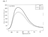
- FIG. 7 is a graph showing light emission wavelength characteristic data according to the ratio of Ce in the light emitting device including the phosphor composition of the embodiment.
- FIG. 8 is an exploded perspective view showing a lighting device having a light emitting device according to the embodiment.
- each layer shown in the drawings may be exaggerated, omitted or schematically drawn for the purpose of convenience or clarity.
- the size of elements does not utterly reflect an actual size.
- FIG. 1 is a sectional view showing a light emitting device package 200 including a phosphor composition according to the first embodiment.
- the package structure according to the first embodiment is not limited thereto, and is applicable to a two cup package type of a package.
- the light emitting device package 200 may include a package body 205, a light emitting device chip 100 on the package body 205 and a molding member 230 including a phosphor composition 232 on the light emitting device chip 100.
- the phosphor composition 232 according to the first embodiment is expressed as a compositional formula of A 3-z C 5 O 12 :RE z (0 ⁇ z ⁇ 0.5), wherein the A may include at least one selected from the group consisting of Y, Sc, Gd and Lu, the C may include at least one selected from the group consisting of B (Boron), Al and Ga, and the RE may include at least one selected from the group consisting of Eu, Ce, Sm, Yb, Dy, Gd, Tm and Lu.
- the phosphor composition 232 according to the first embodiment may include a formula of Y 3 (8 5-x Al x )O 12 :Ce (0 ⁇ x ⁇ 5).
- the phosphor composition 232 according to the second embodiment may include a formula of (Y, Gd) 3-z (B,Al) 5 O 12 :Ce z .
- the phosphor compositions 232 according to the first and second embodiments may have a light emission wavelength in the range of 559 nm to 567 nm with respect to an excitation wavelength in the range of 420 nm to 500 nm.
- the light emitting device package 200 may include a package body 205, first and second electrode layers 213 and 214 mounted on the package body 205, a light emitting device chip 100 mounted on the package body 205 and electrically connected to the first and second electrode layers 213 and 214, and a molding member 230 surrounding the light emitting device chip 100.
- the package body 205 may include a silicon material, a synthetic resin material or a metallic material.
- An inclined surface may be formed around the light emitting device chip 100.
- the first and second electrode layers 213 and 214 are electrically separated from each other, and perform a function of supplying electric power to the light emitting device chip 100.
- the first and second electrode layers 213 and 214 reflect the light generated from the light emitting device chip 100 so that the light efficiency may be increased, and may dissipate the heat generated from the light emitting device 10 to an outside.
- the light emitting device chip 100 may be applied to a lateral-type light emitting device, but the embodiment is not limited thereto.
- the light emitting device chip 100 may be applied to a vertical-type light emitting device or a flip-chip-type light emitting device.
- the light emitting device chip 100 may be formed of a nitride semiconductor.
- the light emitting device chip 100 may include GaN, GaAs, GaAsP or GaP.
- the light emitting device chip 100 may include a light emitting structure including a first conductive semiconductor layer (not shown), an active layer (not shown) and a second conductive semiconductor layer (not shown).
- the first conductive semiconductor layer may include an N type semiconductor layer and the second conductive semiconductor layer may include a P type semiconductor layer, but the embodiment is not limited thereto.
- a semiconductor layer such as an N type semiconductor layer (not shown) having polarity opposite to that of the second conductive semiconductor layer, may be formed on the second conductive semiconductor layer.
- the light emitting structure 110 may include one of an N-P junction structure, a P-N junction structure, an N-P-N junction structure, and a P-N-P junction structure.
- the light emitting device chip 100 may be disposed on the package body 205, or may be disposed on the first or second electrode layer 213 or 214.
- the light emitting device chip 100 may be electrically connected to the first and/or second electrode layer 213 and/or 214 through one of a wire scheme, a flip-chip scheme and a die bonding scheme. Although it is described in the embodiment that the light emitting device chip 100 is electrically connected to the first electrode layer 213 through a first wire and to the second electrode layer 214 through a second wire, the embodiment is not limited thereto.
- the molding member 230 surrounds the light emitting device chip 100 to protect the light emitting device chip 100.
- the phosphor composition 232 is included in the molding member 230 so that the wavelength of light emitted from the light emitting device chip 100 may be changed.
- the phosphor composition 232 has a light emitting region in the yellow region, so that the phosphor composition 232 may be applied for implementing a white LED.
- the phosphor composition 232 may have an excitation wavelength in the range of 420 nm to 500 nm and a yellow-light emission wavelength in the range of 559 nm to 567 nm by the absorption region.
- the yellow phosphor composition 232 according to the embodiment is applicable and utilizable for a UV-LED and a blue LED.
- a conventional scheme of implementing a white LED using a blue LED chip includes a scheme of coating green and red phosphor compositions on a blue LED chip, a yellow phosphor composition and a blue LED chip and a scheme of coating green, red and yellow colors on a blue LED chip, where the phosphor composition of the embodiment signifies a phosphor composition that emits a yellow light and is used to implement a white LED.
- a white LED may be implemented by applying green, red and blue phosphor compositions to a UV-chip, and the color rendering index may be improved by additionally coating the yellow phosphor composition to the white LED.
- the white LED is implemented by using the phosphor composition 232 of the embodiment, the white LED is usable in a field of mobile, vehicle, lamp, backlight unit or medicine.
- a phosphor composition according to the first embodiment is expressed as a compositional formula of A 3-z C 5 O 12 :RE z (0 ⁇ z ⁇ 0.5), where the A may include at least one of selected from the group consisting Y, Sc, Gd and Lu, the C may include at least one selected from the group consisting of B (Boron), Al and Ga, and the RE may include at least one selected from the group consisting of Eu, Ce, Sm, Yb, Dy, Gd, Tm and Lu.
- the phosphor composition 232 of the first embodiment may include the compositional formula of Y 3 (B 5-x Al x )O 12 :Ce (0 ⁇ x ⁇ 5).
- the phosphor composition 232 according to the embodiment has an advantage of being easily fabricated through a solid-state reaction method by using a stable starting material.
- a stable starting material For example, after raw materials of Y 2 O 3 , Al 2 O 3 , B 2 O 3 , CeO 2 and NH 4 Cl are weighed according to the composition ratio of Y 3 B 5-x Al x O 12 :Ce, the raw materials are mixed in an agate mortar with solvent. In this case, the raw materials may be mixed into the composition according to the variation of the ratio of B to Al in the range of 0 ⁇ x ⁇ 5.
- the phosphor composition 232 according to the second embodiment may include the compositional formula of (Y, Gd) 3-z (B,Al) 5 O 12 :Ce z .
- materials may be mixed according to a variation of the ratio of Ce in the basic composition of (Y, Gd) 3-z (B,Al) 5 O 12 :Ce z .
- the z may be 0.1 ⁇ z ⁇ 0.3, but the embodiment is not limited thereto.
- the synthesis atmosphere of the phosphor composition 232 has the condition of a gas flow in the range of 400 cc to 2,000 cc per minute and the synthesis temperature in the range of about 1300°C to about 1500°C.
- the reductive gas may include H 2 , N 2 , and NH 3 .
- the phosphor composition 232 may be synthesized by changing the ratio of H 2 /N 2 mixing gas in the range of 5%/95% to 20%/80%.
- the phosphor composition 232 according to the embodiment is synthesized under the condition in which the reductive gas has a content of 20% of H 2 and 80% of N 2 , the gas flow is 1,000cc/min for about six hours, and the temperature is about 1,400°C, but the embodiment is not limited thereto.
- the fired phosphor composition 232 may be dried after performing a ball milling process and a cleaning process using zirconia and a glass ball.
- the particles of the phosphor composition 232 of the embodiment having the size of about 10 ⁇ m and irregular shapes may be identified based on SEM (Scanning Electron Microscopy) data and the components of the phosphor composition 232 may be identified through EDX (Energy Dispersive X-ray analyzer).
- the excitation light emission characteristic of the dried phosphor composition 232 may be analyzed through PL (Photoluminescence) analysis.
- PL Photoluminescence
- the phosphor composition 232 is a yellow phosphor composition 232 having a light emission wavelength in the range of 559 nm ⁇ 567 nm.
- FIG. 2 is a graph showing excitation wavelength characteristic data according to the ratio of B to A in the light emitting device including the phosphor composition 232 according to the embodiment.
- FIG. 3 is a graph showing light emission wavelength characteristic data according to the ratio of B to Al in the light emitting device including the phosphor composition 232 of the embodiment.
- Table 1 shows characteristic experimental examples of the light emitting device including the phosphor composition 232 of the embodiment according to the ratio of B to Al.
- the light emitting device when the compositional ratio x of Al in the compositional formula of Y 3 (B 5-x Al x )O 12 :Ce is in the range of 1 ⁇ x ⁇ 4, the light emitting device has high reliability and shows an optimal light emission intensity due to its high luminance as compared with the composition of Y 3 B 5 O 12 :Ce.
- Table 1 it may be identified the highest light emission intensity is shown in the experimental example 4, but the embodiment is not limited thereto.
- a phosphor composition 232 according to the third embodiment is expressed as a compositional formula of A 3-z C 5 O 12 :RE z (0 ⁇ z ⁇ 0.5), where the A may include at least one selected from the group consisting of Y, Sc, Gd and Lu, the C may include at least one selected from the group consisting of B (Boron), Al and Ga, and the RE may include at least one selected from the group consisting of Eu, Ce, Sm, Yb, Dy, Gd, Tm and Lu.
- the phosphor composition 232 according to the third embodiment may include a compositional formula of (Gd 3-y-z Y y )B 5 O 12 :Ce z (0 ⁇ y ⁇ 2).
- the phosphor compositions 232 may have a light emission wavelength in the range of 559 nm to 567 nm with respect to an excitation wavelength in the range of 420 nm to 500 nm.
- the phosphor composition 232 according to the first embodiment may include a compositional formula of (Gd 3-y-z Y y )B 5 O 12 :Ce z (0 ⁇ z ⁇ 0.5).
- a phosphor composition 232 may include a compositional formula of (Y, Gd) 3-z (B,Al) 5 O 12 :Ce z .
- materials may be mixed according to a variation of the ratio of Ce in the basic composition of (Y, Gd) 3-z (B 5 Al) 5 O 12 :Ce z .
- the z may be 0.1 ⁇ z ⁇ 0.3, but the embodiment is not limited thereto.
- the phosphor composition 232 according to the embodiment has an advantage of being easily fabricated through a solid-state reaction method by using a stable starting material.
- a stable starting material For example, after raw materials of Y 2 O 3 , Gd 2 O 3 , B 2 O 3 , CeO 2 and NH 4 Cl are weighed according to the composition ratio of (Gd 3-y-z Y y )B 5 O 12 :Ce z , the raw materials are mixed in an agate mortar with solvent. In this case, the raw materials may be mixed into the composition according to the variation of the ratio of Y to Gd in the range of 0 ⁇ y ⁇ 2.
- the synthesis atmosphere of the phosphor composition 232 has the condition of a gas flow in the range of 400 cc to 2,000 cc per minute and the synthesis temperature in the range of about 1300°C to about 1500°C.
- the reductive gas may include H 2 , N 2 , and NH 3 .
- the phosphor composition 232 may be synthesized by changing the ratio of H 2 /N 2 mixing gas in the range of 5%/95% to 20%/80%.
- the phosphor composition 232 according to the embodiment is synthesized under the condition in which a reductive gas has a content of 20% of H 2 and 80% of N 2 , the gas flow is 1,000 cc/min for about six hours, and the temperature is about 1,400°C, but the embodiment is not limited thereto.
- the fired phosphor composition 232 may be dried after performing a ball milling process and a cleaning process using zirconia and a glass ball.
- the particles of the phosphor composition 232 of the embodiment having the size of about 10 ⁇ m and irregular shapes may be identified based on SEM (Scanning Electron Microscopy) data and the components of the phosphor composition 232 may be identified through EDX (Energy Dispersive X-ray analyzer).
- the excitation light emission characteristic of the dried phosphor composition 232 may be analyzed through PL analysis.
- the phosphor composition 232 is a yellow phosphor composition 232 having a light emission wavelength in the range of 559 nm ⁇ 567 nm.
- FIG. 4 is a graph showing excitation wavelength characteristic data according to the ratio of Y to Gd in the light emitting device including the phosphor composition 232 according to the embodiment.
- FIG. 5 is a graph showing light emission wavelength characteristic data according to the ratio of Y to Gd in the light emitting device including the phosphor composition 232 of the embodiment.
- Table 2 Experimental example Ratio ofY to Gd Composition Relative intensity Center wavelength (nm)
- Table 2 shows characteristic experimental examples of the light emitting device including the phosphor composition 232 of the embodiment according to the ratio ofY to Gd.
- the light emitting device when the compositional ratio y of Y in the compositional formula of (Gd 3-y-z Y y )B 5 O 12 :Ce z is in the range of 0 ⁇ y ⁇ 2, the light emitting device has high reliability and shows an optimal light emission intensity due to its high luminance as compared with the related art.
- a new yellow phosphor composition of emitting yellow light which has not been proposed in the related art, may be provided by including the composition formula of (Gd 3-y-z Y y )B 5 O 12 :Ce z or Gd) 3-z (B,Al) 5 O 12 :Ce z .
- FIG. 6 is a graph showing excitation wavelength characteristic data according to the ratio of Ce in the light emitting device including the phosphor composition 232 according to the embodiment.
- FIG. 7 is a graph showing light emission wavelength characteristic data according to the ratio of Ce in the light emitting device including the phosphor composition 232 of the embodiment.
- Table 3 Experimental example Ratio of Ce Composition Relative intensity Center wavelength (mm)
- Experimental example 9(Spl 9) 0.1 (Y, Gd) 3 (B,Al) 5 O 12 :Ce 0.1 100 559
- Experimental example 10(Spl 10) 0.2 (Y, Gd) 3 (B,Al) 5 O 12 :Ce 0.2 129.9
- Table 3 shows characteristic experimental examples of the light emitting device including the phosphor composition 232 of the embodiment according to the ratio of Ce.
- the light emitting device when the compositional ratio z of RE in the compositional formula of A 3-z C 5 O 12 :RE z is in the range of 0.1 ⁇ z ⁇ 0.3, the light emitting device shows a high light emission intensity as compared with the related art. Specifically, as the results shown in Table 2, when the ratio of Ce is 0.2 (Experimental example 10), it has been identified that the maximum light emission intensity is outputted, but the embodiment is not limited to experimental example 10.
- the phosphor composition disclosed above includes a compositional formula of A z C x O 12 :RE, where the z is 0 ⁇ z ⁇ 3, the x is 0 ⁇ x ⁇ 5, the A includes at least one of Y, Sc, Gd and Lu, the C includes at least one selected from the group consisting of B(Boron), Al and Ga, and the RE is at least one selected from the group consisting of Eu, Ce, Sm, Yb, Dy, Gd, Tm and Lu.
- the phosphor composition emits yellow light and includes at least one of the compositional formula of Y 3 B 5-x Al x O 12 :Ce, Gd 3-y-z Y y B 5 O 12 :Ce and (Y, Gd) 3-z (B,Al) 5 O 12 :Ce v , where the x is in the range of 0 ⁇ x ⁇ 5, the Y is in the range of 0 ⁇ y ⁇ 2, the z is in the range of 0 ⁇ z ⁇ 3, and the v is in the range of 0.1 ⁇ v ⁇ 0.3.
- FIG. 8 is an exploded perspective view showing a lighting device having the light emitting device according to the embodiment.
- the lighting system according to the embodiment may include a cover 2100, a light source module 2200, a radiator 2400, a power supply part 2600, an inner case 2700, and a socket 2800.
- the lighting device according to the embodiment may further include at least one of a member 2300 and a holder 2500.
- the light source module 2200 may include the light emitting device according to the embodiment.
- the cover 2100 may have a blub shape, a hemisphere shape, a partially-open hollow shape.
- the cover 2100 may be optically coupled with the light source module 2200.
- the cover 2100 may diffuse, scatter, or excite light provided from the light source module.
- the cover 2100 may be a type of optical member.
- the cover 2100 may be coupled with the radiator 2400.
- the cover 2100 may include a coupling part which is coupled with the radiator 2400.
- the cover 2100 may include an inner surface coated with a milk-white paint.
- the milk-white paint may include a diffusion material to diffuse light.
- the cover 2100 may have the inner surface of which surface roughness is greater than that of the outer surface thereof. The surface roughness is provided for the purpose of sufficiently scattering and diffusing the light from the light source module 2200.
- a material of the cover 2100 may include glass, plastic, polypropylene (PP), polyethylene (PE), and polycarbonate (PC).
- the polycarbonate (PC) has the superior light resistance, heat resistance and strength among the above materials.
- the cover 2100 may be transparent so that a user may view the light source module 2200 from the outside, or opaque.
- the cover 2100 may be formed through a blow molding scheme.
- the light source module 2200 may be disposed at one surface of the radiator 2400. Accordingly, the heat from the light source module 2200 is transferred to the radiator 2400.
- the light source module 2200 may include a light source 2210, a connection plate 2230, and a connector 2250.
- the member 2300 is disposed at a top surface of the radiator 2400, and includes guide grooves 2310 into which a plurality of light sources 2210 and the connector 2250 are inserted.
- the guide grooves 2310 correspond to a substrate of the light source 2210 and the connector 2250.
- a surface of the member 2300 may be coated with a light reflective material.
- the surface of the member 2300 may be coated with white paint.
- the member 2300 again reflects light, which is reflected by the inner surface of the cover 2100 and is returned to the direction of the light source module 2200, to the direction of the cover 2100. Accordingly, the light efficiency of the lighting device according to the embodiment may be improved.
- the member 2300 may include an insulating material.
- the connection plate 2230 of the light source module 2200 may include an electrically conductive material.
- the radiator 2400 may be electrically connected to the connection plate 2230.
- the member 2300 may be configured by an insulating material, thereby preventing the connection plate 2230 from being electrically shorted with the radiator 2400.
- the radiator 2400 receives and radiates heats from the light source module 2200 and the power supply part 2600.
- the holder 2500 covers a receiving groove 2719 of an insulating part 2710 of an inner case 2700. Accordingly, the power supply part 2600 received in the insulating part 2710 of the inner case 2700 is closed.
- the holder 2500 includes a guide protrusion 2510.
- the guide protrusion 2510 has a hole through a protrusion of the power supply part 2600.
- the power supply part 2600 processes or converts an electric signal received from the outside and provides the processed or converted electric signal to the light source module 2200.
- the power supply part 2600 is received in a receiving groove 2719 of the inner case 2700, and is closed inside the inner case 2700 by the holder 2500.
- the power supply part 2600 may include a protrusion 2610, a guide part 2630, a base 2650, and an extension part 2670.
- the guide part 2630 has a shape protruding from one side of the base 2650 to the outside.
- the guide part 2630 may be inserted into the holder 2500.
- a plurality of components may be disposed above one surface of the base 2650.
- the components may include a DC converter converting AC power provided from an external power supply into DC power, a driving chip controlling driving of the light source module 2200, and an electrostatic discharge (ESD) protection device protecting the light source module 2200, but the embodiment is not limited thereto.
- the extension part 2670 has a shape protruding from an opposite side of the base 2650 to the outside.
- the extension part 2670 is inserted into an inside of the connection part 2750 of the inner case 2700, and receives an electric signal from the outside.
- a width of the extension part 2670 may be smaller than or equal to a width of the connection part 2750 of the inner case 2700.
- First terminals of a "+ electric wire” and a "- electric wire” are electrically connected to the extension part 2670 and second terminals of the "+ electric wire” and the "- electric wire” may be electrically connected to the socket 2800.
- the inner case 2700 may include a molding part therein together with the power supply part 2600.
- the molding part is prepared by hardening molding liquid, and the power supply part 2600 may be fixed inside the inner case 2700 by the molding part.
- a phosphor composition having improved reliability and a high luminance, and a light emitting apparatus having the same may be provided.
- the embodiment may provide a phosphor composition having high light emission intensity and a light emitting apparatus having the same.
- any reference in this specification to "one embodiment,” “an embodiment,” “example embodiment,” etc. means that a particular feature, structure, or characteristic described in connection with the embodiment is included in at least one embodiment of the invention.
- the appearances of such phrases in various places in the specification are not necessarily all referring to the same embodiment.
Landscapes
- Chemical & Material Sciences (AREA)
- Inorganic Chemistry (AREA)
- Engineering & Computer Science (AREA)
- Materials Engineering (AREA)
- Organic Chemistry (AREA)
- Luminescent Compositions (AREA)
- Led Device Packages (AREA)
- Non-Portable Lighting Devices Or Systems Thereof (AREA)
Abstract
Description
- The embodiment relates to a phosphor composition and a light emitting apparatus including the same. The light emitting apparatus may include a light emitting device package, a lighting unit or a backlight unit.
- An LED (Light Emitting Device) is a device having a property of converting electrical energy into light energy. For example, the LED may represent various colors by adjusting the compositional ratio of compound semiconductors.
- For instance, a nitride semiconductor represents superior thermal stability and wide band gap energy so that the nitride semiconductor has been spotlighted in the field of optical devices and high-power electronic devices. In particular, blue, green, and UV light emitting devices employing the nitride semiconductor have already been commercialized and extensively used.
- An LED of emitting white color light, which employs a secondary light source of emitting light by coating phosphor, is generally implemented through a scheme of coating YAG:Ce phosphor of generating yellow color light on a blue LED.
- However, according to the scheme described above, due to quantum deficits and reradiation efficiency caused by secondary light, the efficiency is reduced and the color rendering is not easy.
- Thus, since a blue LED is combined with yellow phosphor in a white LED backlight of the related art, the white LED backlight lacks of green and red components, so that colors are unnaturally represented. For this reason, the white LED backlight has been limitedly applied to a display of a portable phone or a laptop computer. Nevertheless, the white LED backlight according to the related art has been extensively used because the white LED backlight is easily driven and inexpensive.
- Generally, it is well known in the art that the phosphor material may include a silicate, a phosphate, an aluminate, or a sulfide and a transition metal or a rare-earth metal is used at the center of light emission. For example, although silicate phosphor has been used for a backlight unit or a lighting device, the silicate phosphor is weak to moisture so the reliability of the silicate phosphor is inferior to any other phosphors.
- Meanwhile, although a phosphor for a white LED, which is excited by an excitation source having high energy such as ultraviolet light or blue light to emit visible light, has been mainly developed, if the phosphor according to the related art is exposed to the excitation source, the luminance of the phosphor is reduced.
- The embodiment provides a phosphor composition having improved reliability and a high luminance, and a light emitting apparatus having the same.
- Further, the embodiment provides a phosphor composition having high light emission intensity and a light emitting apparatus having the same.
- The embodiment provides a yellow phosphor having a new composition and a light emitting apparatus having the same.
- Further, the embodiment provides a phosphor composition having improved reliability and a high luminance, and a light emitting apparatus having the same.
- In addition, the embodiment provides a phosphor composition having high light emission intensity and a light emitting apparatus having the same.
- A phosphor composition according to the embodiment is expressed as a compositional formula of AzCxO12:RE (0 < z≤0.5), wherein the A may include at least one selected from the group consisting of Y, Sc, Gd and Lu, the C may include at least one selected from the group consisting of Al and Ga, and the RE may include at least one selected from the group consisting of Eu, Ce, Sm, Yb, Dy, Gd, Tm and Lu.
- A phosphor composition according to the embodiment is expressed as a compositional formula of A3-zC5O12:REz (0 < z≤0.5), wherein the A may include at least one selected from the group consisting of Y, Sc, Gd and Lu, the C may include at least one selected from the group consisting of Al and Ga, the RE may include at least one selected from the group consisting of Eu, Ce, Sm, Yb, Dy, Gd, Tm and Lu, and the compositional formula of A3-zC5012:REz may include a compositional formula of (Y, Gd)3-z(B,Al)5O12:Ce.
- A phosphor composition according to the embodiment is expressed as a compositional formula of A3-zC5O12:REz (0 <z≤0.5), wherein the A may include at least one selected from the group consisting of Y, Sc, Gd and Lu, the C may include at least one selected from the group consisting of B (Boron), Al and Ga, the RE may include at least one selected from the group consisting of Eu, Ce, Sm, Yb, Dy, Gd, Tm and Lu, and the compositional formula of A3-zC5012:REz may include a compositional formula of (Gd3-y-zYy)B5O12:Cez (0≤y≤2).
- A light emitting device package according to the embodiment includes a body; first and second electrode layers on the body; a light emitting chip electrically connected to the first and second electrode layers; and a molding member including a phosphor composition on a light emitting chip, wherein the phosphor composition includes a compositional formula of AzCxO12:RE, the z is 0≤z≤3 and the x is 0≤x≤5, the A includes at least one selected from the group consisting of Y, Sc, Gd and Lu, the C includes at least one selected from the group consisting of B (Boron), Al and Ga, the RE is at least one selected from the group consisting of Eu, Ce, Sm, Yb, Dy, Gd, Tm and Lu, and the phosphor composition emits yellow light.
-
FIG. 1 is a sectional view showing a light emitting device package including a phosphor composition according to the embodiment. -
FIG. 2 is a graph showing excitation wavelength characteristic data according to the ratio of B to Al in the light emitting device including the phosphor composition of the embodiment. -
FIG. 3 is a graph showing light emission wavelength characteristic data according to the ratio of B to Al in the light emitting device including the phosphor composition of the embodiment. -
FIG. 4 is a graph showing excitation wavelength characteristic data according to the ratio of Y to Gd in the light emitting device including the phosphor composition according to the embodiment. -
FIG. 5 is a graph showing light emission wavelength characteristic data according to the ratio of Y to Gd in the light emitting device including the phosphor composition of the embodiment. -
FIG. 6 is a graph showing excitation wavelength characteristic data according to the ratio of Ce in the light emitting device including the phosphor composition according to the embodiment. -
FIG. 7 is a graph showing light emission wavelength characteristic data according to the ratio of Ce in the light emitting device including the phosphor composition of the embodiment. -
FIG. 8 is an exploded perspective view showing a lighting device having a light emitting device according to the embodiment. - In the description of the embodiments, it will be understood that, when a layer (or film), a region, a pattern, or a structure is referred to as being "on" or "under" another substrate, another layer (or film), another region, another pad, or another pattern, it can be "directly" or "indirectly" over the other substrate, layer (or film), region, pad, or pattern, or one or more intervening layers may also be present. Such a position of the layer has been described with reference to the drawings.
- The thickness and size of each layer shown in the drawings may be exaggerated, omitted or schematically drawn for the purpose of convenience or clarity. In addition, the size of elements does not utterly reflect an actual size.
- (Embodiment)
-
FIG. 1 is a sectional view showing a lightemitting device package 200 including a phosphor composition according to the first embodiment. The package structure according to the first embodiment is not limited thereto, and is applicable to a two cup package type of a package. - The light
emitting device package 200 may include apackage body 205, a lightemitting device chip 100 on thepackage body 205 and amolding member 230 including aphosphor composition 232 on the lightemitting device chip 100. - The
phosphor composition 232 according to the first embodiment is expressed as a compositional formula of A3-zC5O12:REz (0 < z≤0.5), wherein the A may include at least one selected from the group consisting of Y, Sc, Gd and Lu, the C may include at least one selected from the group consisting of B (Boron), Al and Ga, and the RE may include at least one selected from the group consisting of Eu, Ce, Sm, Yb, Dy, Gd, Tm and Lu. - The
phosphor composition 232 according to the first embodiment may include a formula of Y3(85-xAlx)O12:Ce (0≤x < 5). - In addition, the
phosphor composition 232 according to the second embodiment may include a formula of (Y, Gd)3-z(B,Al)5O12:Cez. - The
phosphor compositions 232 according to the first and second embodiments may have a light emission wavelength in the range of 559 nm to 567 nm with respect to an excitation wavelength in the range of 420 nm to 500 nm. - The light
emitting device package 200 according to the embodiment may include apackage body 205, first andsecond electrode layers package body 205, a lightemitting device chip 100 mounted on thepackage body 205 and electrically connected to the first andsecond electrode layers molding member 230 surrounding the lightemitting device chip 100. - The
package body 205 may include a silicon material, a synthetic resin material or a metallic material. An inclined surface may be formed around the lightemitting device chip 100. - The first and
second electrode layers emitting device chip 100. In addition, the first andsecond electrode layers emitting device chip 100 so that the light efficiency may be increased, and may dissipate the heat generated from thelight emitting device 10 to an outside. - The light
emitting device chip 100 may be applied to a lateral-type light emitting device, but the embodiment is not limited thereto. The lightemitting device chip 100 may be applied to a vertical-type light emitting device or a flip-chip-type light emitting device. - The light
emitting device chip 100 may be formed of a nitride semiconductor. For example, the lightemitting device chip 100 may include GaN, GaAs, GaAsP or GaP. - The light
emitting device chip 100 may include a light emitting structure including a first conductive semiconductor layer (not shown), an active layer (not shown) and a second conductive semiconductor layer (not shown). - According to the embodiment, the first conductive semiconductor layer may include an N type semiconductor layer and the second conductive semiconductor layer may include a P type semiconductor layer, but the embodiment is not limited thereto. In addition, a semiconductor layer, such as an N type semiconductor layer (not shown) having polarity opposite to that of the second conductive semiconductor layer, may be formed on the second conductive semiconductor layer. Thus, the light emitting structure 110 may include one of an N-P junction structure, a P-N junction structure, an N-P-N junction structure, and a P-N-P junction structure.
- The light
emitting device chip 100 may be disposed on thepackage body 205, or may be disposed on the first orsecond electrode layer - The light
emitting device chip 100 may be electrically connected to the first and/orsecond electrode layer 213 and/or 214 through one of a wire scheme, a flip-chip scheme and a die bonding scheme. Although it is described in the embodiment that the lightemitting device chip 100 is electrically connected to thefirst electrode layer 213 through a first wire and to thesecond electrode layer 214 through a second wire, the embodiment is not limited thereto. - The
molding member 230 surrounds the lightemitting device chip 100 to protect the lightemitting device chip 100. Thephosphor composition 232 is included in themolding member 230 so that the wavelength of light emitted from the lightemitting device chip 100 may be changed. - Since the
phosphor composition 232 according to the embodiment has a light emitting region in the yellow region, so that thephosphor composition 232 may be applied for implementing a white LED. - For example, the
phosphor composition 232 may have an excitation wavelength in the range of 420 nm to 500 nm and a yellow-light emission wavelength in the range of 559 nm to 567 nm by the absorption region. - The
yellow phosphor composition 232 according to the embodiment is applicable and utilizable for a UV-LED and a blue LED. - For example, a conventional scheme of implementing a white LED using a blue LED chip includes a scheme of coating green and red phosphor compositions on a blue LED chip, a yellow phosphor composition and a blue LED chip and a scheme of coating green, red and yellow colors on a blue LED chip, where the phosphor composition of the embodiment signifies a phosphor composition that emits a yellow light and is used to implement a white LED.
- According to the embodiment, a white LED may be implemented by applying green, red and blue phosphor compositions to a UV-chip, and the color rendering index may be improved by additionally coating the yellow phosphor composition to the white LED.
- When the white LED is implemented by using the
phosphor composition 232 of the embodiment, the white LED is usable in a field of mobile, vehicle, lamp, backlight unit or medicine. - Hereinafter, the features of the embodiment will be described in more detail with reference to the process of fabricating a phosphor composition according to the embodiment.
- A phosphor composition according to the first embodiment is expressed as a compositional formula of A3-zC5O12:REz (0 < z≤0.5), where the A may include at least one of selected from the group consisting Y, Sc, Gd and Lu, the C may include at least one selected from the group consisting of B (Boron), Al and Ga, and the RE may include at least one selected from the group consisting of Eu, Ce, Sm, Yb, Dy, Gd, Tm and Lu.
- For example, the
phosphor composition 232 of the first embodiment may include the compositional formula of Y3(B5-xAlx)O12:Ce (0≤x < 5). - The
phosphor composition 232 according to the embodiment has an advantage of being easily fabricated through a solid-state reaction method by using a stable starting material. For example, after raw materials of Y2O3, Al2O3, B2O3, CeO2 and NH4Cl are weighed according to the composition ratio of Y3B5-xAlxO12:Ce, the raw materials are mixed in an agate mortar with solvent. In this case, the raw materials may be mixed into the composition according to the variation of the ratio of B to Al in the range of 0≤x < 5. - In addition, the
phosphor composition 232 according to the second embodiment may include the compositional formula of (Y, Gd)3-z(B,Al)5O12:Cez. For example, materials may be mixed according to a variation of the ratio of Ce in the basic composition of (Y, Gd)3-z(B,Al)5O12:Cez. The z may be 0.1≤z≤0.3, but the embodiment is not limited thereto. - The synthesis atmosphere of the
phosphor composition 232 has the condition of a gas flow in the range of 400 cc to 2,000 cc per minute and the synthesis temperature in the range of about 1300°C to about 1500°C. The reductive gas may include H2, N2, and NH3. In this case, thephosphor composition 232 may be synthesized by changing the ratio of H2/N2 mixing gas in the range of 5%/95% to 20%/80%. - For example, the
phosphor composition 232 according to the embodiment is synthesized under the condition in which the reductive gas has a content of 20% of H2 and 80% of N2, the gas flow is 1,000cc/min for about six hours, and the temperature is about 1,400°C, but the embodiment is not limited thereto. - Then, the fired
phosphor composition 232 may be dried after performing a ball milling process and a cleaning process using zirconia and a glass ball. - The particles of the
phosphor composition 232 of the embodiment having the size of about 10 µm and irregular shapes may be identified based on SEM (Scanning Electron Microscopy) data and the components of thephosphor composition 232 may be identified through EDX (Energy Dispersive X-ray analyzer). - As shown in
FIGS. 2 and3 , the excitation light emission characteristic of the driedphosphor composition 232 may be analyzed through PL (Photoluminescence) analysis. In cases of Y3B5-xAlxO12:Ce and (Y,Gd)3-z(B,Al)5O12:Cez according to a condition change, it may be known that thephosphor composition 232 is ayellow phosphor composition 232 having a light emission wavelength in the range of 559 nm ∼ 567 nm. -
FIG. 2 is a graph showing excitation wavelength characteristic data according to the ratio of B to A in the light emitting device including thephosphor composition 232 according to the embodiment. -
FIG. 3 is a graph showing light emission wavelength characteristic data according to the ratio of B to Al in the light emitting device including thephosphor composition 232 of the embodiment. - Table 1 shows characteristic experimental examples of the light emitting device including the
phosphor composition 232 of the embodiment according to the ratio of B to Al.[Table 1] Experimental example Ratio of B to Al Composition Relative intensity Center wavelength (mm) Experimental example 1 (Spl 1) B=5, Al=0 Y3B5O12: Ce 100 560 Experimental example 2 (Spl 2) B=4, Al=1 Y3B4Al1O12:Ce 124.8 563 Experimental example 3 (Spl 3) B=3, Al=2 Y3B3Al2O12:Ce 137.5 559 Experimental example 4 (Spl 4) B=2, Al=3 Y3B2Al3O12:Ce 162.4 561 Experimental example 5 (Spl 5) B=1, Al=4 Y3B1Al4O12:Ce 150.1 560 - According to the embodiment, when the compositional ratio x of Al in the compositional formula of Y3(B5-xAlx)O12:Ce is in the range of 1≤x≤4, the light emitting device has high reliability and shows an optimal light emission intensity due to its high luminance as compared with the composition of Y3B5O12:Ce. For example, as shown in Table 1, it may be identified the highest light emission intensity is shown in the experimental example 4, but the embodiment is not limited thereto.
- A
phosphor composition 232 according to the third embodiment is expressed as a compositional formula of A3-zC5O12:REz (0 < z≤0.5), where the A may include at least one selected from the group consisting of Y, Sc, Gd and Lu, the C may include at least one selected from the group consisting of B (Boron), Al and Ga, and the RE may include at least one selected from the group consisting of Eu, Ce, Sm, Yb, Dy, Gd, Tm and Lu. - The
phosphor composition 232 according to the third embodiment may include a compositional formula of (Gd3-y-zYy)B5O12:Cez (0≤y≤2). Thephosphor compositions 232 may have a light emission wavelength in the range of 559 nm to 567 nm with respect to an excitation wavelength in the range of 420 nm to 500 nm. For example, thephosphor composition 232 according to the first embodiment may include a compositional formula of (Gd3-y-zYy)B5O12:Cez (0 < z≤0.5). - A
phosphor composition 232 according to still another embodiment may include a compositional formula of (Y, Gd)3-z(B,Al)5O12:Cez. For example, materials may be mixed according to a variation of the ratio of Ce in the basic composition of (Y, Gd)3-z(B5Al)5O12:Cez. The z may be 0.1≤z≤0.3, but the embodiment is not limited thereto. - The
phosphor composition 232 according to the embodiment has an advantage of being easily fabricated through a solid-state reaction method by using a stable starting material. For example, after raw materials of Y2O3, Gd2O3, B2O3, CeO2 and NH4Cl are weighed according to the composition ratio of (Gd3-y-zYy)B5O12:Cez, the raw materials are mixed in an agate mortar with solvent. In this case, the raw materials may be mixed into the composition according to the variation of the ratio of Y to Gd in the range of 0≤y < 2. - The synthesis atmosphere of the
phosphor composition 232 has the condition of a gas flow in the range of 400 cc to 2,000 cc per minute and the synthesis temperature in the range of about 1300°C to about 1500°C. The reductive gas may include H2, N2, and NH3. In this case, thephosphor composition 232 may be synthesized by changing the ratio of H2/N2 mixing gas in the range of 5%/95% to 20%/80%. For example, thephosphor composition 232 according to the embodiment is synthesized under the condition in which a reductive gas has a content of 20% of H2 and 80% of N2, the gas flow is 1,000 cc/min for about six hours, and the temperature is about 1,400°C, but the embodiment is not limited thereto. - Then, the fired
phosphor composition 232 may be dried after performing a ball milling process and a cleaning process using zirconia and a glass ball. - The particles of the
phosphor composition 232 of the embodiment having the size of about 10 µm and irregular shapes may be identified based on SEM (Scanning Electron Microscopy) data and the components of thephosphor composition 232 may be identified through EDX (Energy Dispersive X-ray analyzer). - As shown in
FIGS. 4 and5 , the excitation light emission characteristic of the driedphosphor composition 232 may be analyzed through PL analysis. In cases of (Gd3-y-zYy)B5O12:Cez or (Y,Gd)3-z(B,Al)5O12:Cez according to a condition change, it may be known that thephosphor composition 232 is ayellow phosphor composition 232 having a light emission wavelength in the range of 559 nm ∼ 567 nm. -
FIG. 4 is a graph showing excitation wavelength characteristic data according to the ratio of Y to Gd in the light emitting device including thephosphor composition 232 according to the embodiment. -
FIG. 5 is a graph showing light emission wavelength characteristic data according to the ratio of Y to Gd in the light emitting device including thephosphor composition 232 of the embodiment.[Table 2] Experimental example Ratio ofY to Gd Composition Relative intensity Center wavelength (nm) Experimental example 6(Spl 6) Y=0, Gd=3 Gd3B5O12: Ce 100 559 Experimental example 7(Spl 7) Y=1, Gd=2 Y1Gd2B5O12:Ce 87.2 562 Experimental example 8(Spl 8) Y=2, Gd=1 Y2Gd1B5O12:Ce 83.4 567 - Table 2 shows characteristic experimental examples of the light emitting device including the
phosphor composition 232 of the embodiment according to the ratio ofY to Gd. - According to the embodiment, when the compositional ratio y of Y in the compositional formula of (Gd3-y-zYy)B5O12:Cez is in the range of 0≤y≤2, the light emitting device has high reliability and shows an optimal light emission intensity due to its high luminance as compared with the related art.
- As shown in
FIG. 5 , according to the embodiment, a new yellow phosphor composition of emitting yellow light, which has not been proposed in the related art, may be provided by including the composition formula of (Gd3-y-zYy)B5O12:Cez or Gd)3-z(B,Al)5O12:Cez. -
FIG. 6 is a graph showing excitation wavelength characteristic data according to the ratio of Ce in the light emitting device including thephosphor composition 232 according to the embodiment. -
FIG. 7 is a graph showing light emission wavelength characteristic data according to the ratio of Ce in the light emitting device including thephosphor composition 232 of the embodiment.[Table 3] Experimental example Ratio of Ce Composition Relative intensity Center wavelength (mm) Experimental example 9(Spl 9) 0.1 (Y, Gd)3(B,Al)5O12: Ce 0.1100 559 Experimental example 10(Spl 10) 0.2 (Y, Gd)3(B,Al)5O12:Ce0.2 129.9 560 Experimental example 11(Spl 11) 0.3 (Y, Gd)3(B,Al)5O12:Ce0.3 103.9 564 - Table 3 shows characteristic experimental examples of the light emitting device including the
phosphor composition 232 of the embodiment according to the ratio of Ce. - According to the embodiment, when the compositional ratio z of RE in the compositional formula of A3-zC5O12:REz is in the range of 0.1≤z≤0.3, the light emitting device shows a high light emission intensity as compared with the related art. Specifically, as the results shown in Table 2, when the ratio of Ce is 0.2 (Experimental example 10), it has been identified that the maximum light emission intensity is outputted, but the embodiment is not limited to experimental example 10.
- The phosphor composition disclosed above includes a compositional formula of AzCxO12:RE, where the z is 0≤z≤3, the x is 0≤x≤5, the A includes at least one of Y, Sc, Gd and Lu, the C includes at least one selected from the group consisting of B(Boron), Al and Ga, and the RE is at least one selected from the group consisting of Eu, Ce, Sm, Yb, Dy, Gd, Tm and Lu. The phosphor composition emits yellow light and includes at least one of the compositional formula of Y3B5-xAlxO12:Ce, Gd3-y-zYyB5O12:Ce and (Y, Gd)3-z(B,Al)5O12:Cev, where the x is in the range of 0≤x≤5, the Y is in the range of 0≤y≤2, the z is in the range of 0≤z≤3, and the v is in the range of 0.1≤v≤0.3.
-
FIG. 8 is an exploded perspective view showing a lighting device having the light emitting device according to the embodiment. - Referring to
FIG. 8 , the lighting system according to the embodiment may include acover 2100, alight source module 2200, aradiator 2400, apower supply part 2600, aninner case 2700, and asocket 2800. The lighting device according to the embodiment may further include at least one of amember 2300 and aholder 2500. Thelight source module 2200 may include the light emitting device according to the embodiment. - For example, the
cover 2100 may have a blub shape, a hemisphere shape, a partially-open hollow shape. Thecover 2100 may be optically coupled with thelight source module 2200. For example, thecover 2100 may diffuse, scatter, or excite light provided from the light source module. Thecover 2100 may be a type of optical member. Thecover 2100 may be coupled with theradiator 2400. Thecover 2100 may include a coupling part which is coupled with theradiator 2400. - The
cover 2100 may include an inner surface coated with a milk-white paint. The milk-white paint may include a diffusion material to diffuse light. Thecover 2100 may have the inner surface of which surface roughness is greater than that of the outer surface thereof. The surface roughness is provided for the purpose of sufficiently scattering and diffusing the light from thelight source module 2200. - For example, a material of the
cover 2100 may include glass, plastic, polypropylene (PP), polyethylene (PE), and polycarbonate (PC). The polycarbonate (PC) has the superior light resistance, heat resistance and strength among the above materials. Thecover 2100 may be transparent so that a user may view thelight source module 2200 from the outside, or opaque. Thecover 2100 may be formed through a blow molding scheme. - The
light source module 2200 may be disposed at one surface of theradiator 2400. Accordingly, the heat from thelight source module 2200 is transferred to theradiator 2400. Thelight source module 2200 may include alight source 2210, aconnection plate 2230, and aconnector 2250. - The
member 2300 is disposed at a top surface of theradiator 2400, and includesguide grooves 2310 into which a plurality oflight sources 2210 and theconnector 2250 are inserted. Theguide grooves 2310 correspond to a substrate of thelight source 2210 and theconnector 2250. - A surface of the
member 2300 may be coated with a light reflective material. For example, the surface of themember 2300 may be coated with white paint. Themember 2300 again reflects light, which is reflected by the inner surface of thecover 2100 and is returned to the direction of thelight source module 2200, to the direction of thecover 2100. Accordingly, the light efficiency of the lighting device according to the embodiment may be improved. - For example, the
member 2300 may include an insulating material. Theconnection plate 2230 of thelight source module 2200 may include an electrically conductive material. Accordingly, theradiator 2400 may be electrically connected to theconnection plate 2230. Themember 2300 may be configured by an insulating material, thereby preventing theconnection plate 2230 from being electrically shorted with theradiator 2400. Theradiator 2400 receives and radiates heats from thelight source module 2200 and thepower supply part 2600. - The
holder 2500 covers a receivinggroove 2719 of aninsulating part 2710 of aninner case 2700. Accordingly, thepower supply part 2600 received in the insulatingpart 2710 of theinner case 2700 is closed. Theholder 2500 includes aguide protrusion 2510. Theguide protrusion 2510 has a hole through a protrusion of thepower supply part 2600. - The
power supply part 2600 processes or converts an electric signal received from the outside and provides the processed or converted electric signal to thelight source module 2200. Thepower supply part 2600 is received in a receivinggroove 2719 of theinner case 2700, and is closed inside theinner case 2700 by theholder 2500. - The
power supply part 2600 may include aprotrusion 2610, aguide part 2630, abase 2650, and anextension part 2670. - The
guide part 2630 has a shape protruding from one side of the base 2650 to the outside. Theguide part 2630 may be inserted into theholder 2500. A plurality of components may be disposed above one surface of thebase 2650. For example, the components may include a DC converter converting AC power provided from an external power supply into DC power, a driving chip controlling driving of thelight source module 2200, and an electrostatic discharge (ESD) protection device protecting thelight source module 2200, but the embodiment is not limited thereto. - The
extension part 2670 has a shape protruding from an opposite side of the base 2650 to the outside. Theextension part 2670 is inserted into an inside of theconnection part 2750 of theinner case 2700, and receives an electric signal from the outside. For example, a width of theextension part 2670 may be smaller than or equal to a width of theconnection part 2750 of theinner case 2700. First terminals of a "+ electric wire" and a "- electric wire" are electrically connected to theextension part 2670 and second terminals of the "+ electric wire" and the "- electric wire" may be electrically connected to thesocket 2800. - The
inner case 2700 may include a molding part therein together with thepower supply part 2600. The molding part is prepared by hardening molding liquid, and thepower supply part 2600 may be fixed inside theinner case 2700 by the molding part. - According to the embodiment, a phosphor composition having improved reliability and a high luminance, and a light emitting apparatus having the same may be provided.
- In addition, the embodiment may provide a phosphor composition having high light emission intensity and a light emitting apparatus having the same.
- Any reference in this specification to "one embodiment," "an embodiment," "example embodiment," etc., means that a particular feature, structure, or characteristic described in connection with the embodiment is included in at least one embodiment of the invention. The appearances of such phrases in various places in the specification are not necessarily all referring to the same embodiment. Further, when a particular feature, structure, or characteristic is described in connection with any embodiment, it is submitted that it is within the purview of one skilled in the art to effect such feature, structure, or characteristic in connection with other ones of the embodiments.
- Although embodiments have been described with reference to a number of illustrative embodiments thereof, it should be understood that numerous other modifications and embodiments can be devised by those skilled in the art that will fall within the spirit and scope of the principles of this disclosure. More particularly, various variations and modifications are possible in the component parts and/or arrangements of the subject combination arrangement within the scope of the disclosure, the drawings and the appended claims. In addition to variations and modifications in the component parts and/or arrangements, alternative uses will also be apparent to those skilled in the art.
Claims (15)
- A phosphor composition having a compositional formula of AzCxO12:RE, wherein the z is 0≤z≤3 and the x is 0≤x≤5,
the A includes at least one selected from the group consisting of Y, Sc, Gd and Lu,
the C includes at least one selected from the group consisting of B, Al and Ga, and
the RE includes at least one selected from the group consisting of Eu, Ce, Sm, Yb, Dy, Gd, Tm and Lu. - The phosphor composition of claim 1, wherein the A is the Y or the Y and the Gd.
- The phosphor composition of claim 2, wherein, in the compositional formula of AzCxO12:RE, the AzCx includes Y3(B5-xAlx).
- The phosphor composition of claim 2, wherein, in the compositional formula of AzCxO12:RE, the Az includes Gd3-y-zYy.
- The phosphor composition of claim 4, wherein, in the compositional formula of AzCxO12:RE, the Az includes Gd3-y-zYy.
- The phosphor composition of claim 4 or 5, wherein the Cx is B5.
- The phosphor composition of claim 1 or 2, wherein the C is B and Al.
- The phosphor composition of claim 7, wherein the Cx is (B, Al)5.
- The phosphor composition of any one of claims 1, 2, 7 and 8, wherein the compositional formula of AzCxO12:RE includes a compositional formula of (Y, Gd)3-z(B,Al)5O12:Cev, and wherein the z is 0.1≤z≤0.3.
- The phosphor composition of any one of claims 1 to 8, wherein the RE is Cev.
- The phosphor composition of claim 9 or 10, wherein the composition(v) of the Cev is 0.1≤z≤0.3.
- The phosphor composition of any one of claims 1 to 11, wherein the phosphor composition has a light emission wavelength in a range of 559 nm to 567 nm with respect to an excitation wavelength in a range of 420 nm to 500 nm.
- A light emitting device package comprising:a body;first and second electrode layers on the body;a light emitting chip electrically connected to the first and second electrode layers; anda molding member including a phosphor composition on the light emitting chip,wherein the phosphor composition is any one of claims 1 to 12.
- The light emitting device package of claim 13, wherein the light emitting chip includes a UV LED chip.
- The light emitting device package of claim 13, wherein the light emitting chip includes a blue LED chip.
Applications Claiming Priority (2)
| Application Number | Priority Date | Filing Date | Title |
|---|---|---|---|
| KR1020120129971A KR102035164B1 (en) | 2012-11-16 | 2012-11-16 | Phosphor compositions |
| KR1020120129972A KR102035169B1 (en) | 2012-11-16 | 2012-11-16 | Phosphor compositions |
Publications (3)
| Publication Number | Publication Date |
|---|---|
| EP2733190A2 true EP2733190A2 (en) | 2014-05-21 |
| EP2733190A3 EP2733190A3 (en) | 2014-09-03 |
| EP2733190B1 EP2733190B1 (en) | 2020-01-01 |
Family
ID=49551538
Family Applications (1)
| Application Number | Title | Priority Date | Filing Date |
|---|---|---|---|
| EP13192060.5A Active EP2733190B1 (en) | 2012-11-16 | 2013-11-08 | Phosphor composition and light emitting device package having the same |
Country Status (4)
| Country | Link |
|---|---|
| US (2) | US20140138728A1 (en) |
| EP (1) | EP2733190B1 (en) |
| JP (1) | JP5868929B2 (en) |
| CN (1) | CN103820118B (en) |
Families Citing this family (4)
| Publication number | Priority date | Publication date | Assignee | Title |
|---|---|---|---|---|
| KR101501020B1 (en) * | 2014-02-17 | 2015-03-13 | 주식회사 루멘스 | Light emitting device package, backlight unit, lighting device and its manufacturing method |
| WO2017111495A1 (en) | 2015-12-23 | 2017-06-29 | 엘지이노텍 주식회사 | Phosphor composition, light-emitting device package comprising same, and lighting apparatus |
| KR102578085B1 (en) | 2016-04-29 | 2023-09-14 | 쑤저우 레킨 세미컨덕터 컴퍼니 리미티드 | Phosphor composition, light emitting device package and lighting apparatus including the same |
| US10361352B1 (en) * | 2018-03-22 | 2019-07-23 | Excellence Opto, Inc. | High heat dissipation light emitting diode package structure having at least two light cups and lateral light emission |
Family Cites Families (19)
| Publication number | Priority date | Publication date | Assignee | Title |
|---|---|---|---|---|
| DE19638667C2 (en) | 1996-09-20 | 2001-05-17 | Osram Opto Semiconductors Gmbh | Mixed-color light-emitting semiconductor component with luminescence conversion element |
| TW383508B (en) * | 1996-07-29 | 2000-03-01 | Nichia Kagaku Kogyo Kk | Light emitting device and display |
| JP2000265169A (en) * | 1999-03-17 | 2000-09-26 | Yiguang Electronic Ind Co Ltd | Production of white light source |
| US6409938B1 (en) * | 2000-03-27 | 2002-06-25 | The General Electric Company | Aluminum fluoride flux synthesis method for producing cerium doped YAG |
| TWI282357B (en) * | 2001-05-29 | 2007-06-11 | Nantex Industry Co Ltd | Process for the preparation of pink light-emitting diode with high brightness |
| CN1318540C (en) * | 2002-09-13 | 2007-05-30 | 北京有色金属研究总院 | Blue light-excitated white phosphor powder for LED and production method thereof |
| KR100610249B1 (en) * | 2003-12-23 | 2006-08-09 | 럭스피아 주식회사 | Yellow light emitting phosphor and white semiconductor light emitting device using the same |
| JP4779384B2 (en) * | 2005-02-28 | 2011-09-28 | 三菱化学株式会社 | Ce-activated rare earth aluminate-based phosphor and light emitting device using the same |
| WO2007015542A1 (en) * | 2005-08-04 | 2007-02-08 | Nichia Corporation | Phosphor and light-emitting device |
| KR100533922B1 (en) * | 2005-08-05 | 2005-12-06 | 알티전자 주식회사 | Yellow phosphor and white light emitting device using there |
| KR101264580B1 (en) | 2005-09-27 | 2013-05-14 | 미쓰비시 가가꾸 가부시키가이샤 | Fluorescent substance, process for producing the same, and light emitting device using said fluorescent substance |
| CN1807547B (en) * | 2006-01-27 | 2011-06-15 | 罗维鸿 | Fluorescent inorganic matter for solid light source |
| US8133461B2 (en) * | 2006-10-20 | 2012-03-13 | Intematix Corporation | Nano-YAG:Ce phosphor compositions and their methods of preparation |
| US9120975B2 (en) * | 2006-10-20 | 2015-09-01 | Intematix Corporation | Yellow-green to yellow-emitting phosphors based on terbium-containing aluminates |
| CN100999662A (en) * | 2006-12-29 | 2007-07-18 | 中国科学院长春应用化学研究所 | Preparation process of fluorescent powder for white light LED excited by blue light |
| CN101113333B (en) * | 2007-08-28 | 2010-12-15 | 厦门大学 | Method for preparing cerium-activated yttrium aluminium garnet fluorescent powder |
| DE102008051029A1 (en) * | 2008-10-13 | 2010-04-15 | Merck Patent Gmbh | Doped garnet phosphors with redshift for pcLEDs |
| TWI361216B (en) * | 2009-09-01 | 2012-04-01 | Ind Tech Res Inst | Phosphors, fabricating method thereof, and light emitting device employing the same |
| TWI418610B (en) * | 2011-03-07 | 2013-12-11 | 財團法人工業技術研究院 | Fluorescent material, and illuminating device comprising the same |
-
2013
- 2013-11-08 EP EP13192060.5A patent/EP2733190B1/en active Active
- 2013-11-12 JP JP2013233977A patent/JP5868929B2/en active Active
- 2013-11-15 CN CN201310572266.9A patent/CN103820118B/en active Active
- 2013-11-15 US US14/081,404 patent/US20140138728A1/en not_active Abandoned
-
2016
- 2016-12-27 US US15/390,980 patent/US10008641B2/en active Active
Also Published As
| Publication number | Publication date |
|---|---|
| CN103820118A (en) | 2014-05-28 |
| US20170110632A1 (en) | 2017-04-20 |
| EP2733190B1 (en) | 2020-01-01 |
| US10008641B2 (en) | 2018-06-26 |
| JP5868929B2 (en) | 2016-02-24 |
| US20140138728A1 (en) | 2014-05-22 |
| JP2014101511A (en) | 2014-06-05 |
| EP2733190A3 (en) | 2014-09-03 |
| CN103820118B (en) | 2016-08-17 |
Similar Documents
| Publication | Publication Date | Title |
|---|---|---|
| CN102227826B (en) | Lighting device for display device and display device | |
| JP2021108381A (en) | White light emitting device | |
| EP2824721B1 (en) | Light emitting device | |
| US20070090381A1 (en) | Semiconductor light emitting device | |
| KR20150005767A (en) | Wavelength-converted element, manufacturing method of the same and semiconductor light emitting apparatus having the same | |
| US10008641B2 (en) | Phosphor composition and light emitting device package having the same | |
| CN104253121A (en) | Omni-directional light-emitting diode device and packaging method thereof | |
| US9559271B2 (en) | Oxynitride-based phosphor and white light emitting device including the same | |
| KR20170073356A (en) | Phosphor, light emitting device having thereof and light unit having thereof | |
| US9190580B2 (en) | Phosphor and light emitting device having the same | |
| KR102035164B1 (en) | Phosphor compositions | |
| KR102035169B1 (en) | Phosphor compositions | |
| KR20180126212A (en) | Light emitting device, light emitting device package comprising the same and lighting apparatus comprising the same | |
| US7737635B2 (en) | High efficiency white light emitting diode and method for manufacturing the same | |
| US10336936B2 (en) | Phosphor and light emitting device having the same | |
| KR102396916B1 (en) | Light emitting device | |
| US20070152562A1 (en) | White light-emitting device | |
| KR101952436B1 (en) | Oxynitride-based phosphor compositions and method for manufacturing the same | |
| KR20160060398A (en) | Light emitting device | |
| KR20210120964A (en) | White light emitting device | |
| KR102288377B1 (en) | Light emitting device | |
| KR20150017595A (en) | Phosphor and light emitting device having thereof | |
| KR20160103743A (en) | Silicone chemical structure, light emitting device and lighting unit | |
| KR20170073360A (en) | Phosphor, light emitting device having thereof and light unit having thereof |
Legal Events
| Date | Code | Title | Description |
|---|---|---|---|
| PUAI | Public reference made under article 153(3) epc to a published international application that has entered the european phase |
Free format text: ORIGINAL CODE: 0009012 |
|
| 17P | Request for examination filed |
Effective date: 20131108 |
|
| AK | Designated contracting states |
Kind code of ref document: A2 Designated state(s): AL AT BE BG CH CY CZ DE DK EE ES FI FR GB GR HR HU IE IS IT LI LT LU LV MC MK MT NL NO PL PT RO RS SE SI SK SM TR |
|
| AX | Request for extension of the european patent |
Extension state: BA ME |
|
| RAP1 | Party data changed (applicant data changed or rights of an application transferred) |
Owner name: LG INNOTEK CO., LTD. |
|
| PUAL | Search report despatched |
Free format text: ORIGINAL CODE: 0009013 |
|
| AK | Designated contracting states |
Kind code of ref document: A3 Designated state(s): AL AT BE BG CH CY CZ DE DK EE ES FI FR GB GR HR HU IE IS IT LI LT LU LV MC MK MT NL NO PL PT RO RS SE SI SK SM TR |
|
| AX | Request for extension of the european patent |
Extension state: BA ME |
|
| RIC1 | Information provided on ipc code assigned before grant |
Ipc: H05B 33/14 20060101ALI20140731BHEP Ipc: C09K 11/78 20060101ALI20140731BHEP Ipc: C09K 11/80 20060101AFI20140731BHEP |
|
| RBV | Designated contracting states (corrected) |
Designated state(s): AL AT BE BG CH CY CZ DE DK EE ES FI FR GB GR HR HU IE IS IT LI LT LU LV MC MK MT NL NO PL PT RO RS SE SI SK SM TR |
|
| 17Q | First examination report despatched |
Effective date: 20160419 |
|
| RAP1 | Party data changed (applicant data changed or rights of an application transferred) |
Owner name: LG INNOTEK CO., LTD. |
|
| STAA | Information on the status of an ep patent application or granted ep patent |
Free format text: STATUS: EXAMINATION IS IN PROGRESS |
|
| GRAP | Despatch of communication of intention to grant a patent |
Free format text: ORIGINAL CODE: EPIDOSNIGR1 |
|
| STAA | Information on the status of an ep patent application or granted ep patent |
Free format text: STATUS: GRANT OF PATENT IS INTENDED |
|
| INTG | Intention to grant announced |
Effective date: 20190626 |
|
| GRAS | Grant fee paid |
Free format text: ORIGINAL CODE: EPIDOSNIGR3 |
|
| GRAA | (expected) grant |
Free format text: ORIGINAL CODE: 0009210 |
|
| STAA | Information on the status of an ep patent application or granted ep patent |
Free format text: STATUS: THE PATENT HAS BEEN GRANTED |
|
| AK | Designated contracting states |
Kind code of ref document: B1 Designated state(s): AL AT BE BG CH CY CZ DE DK EE ES FI FR GB GR HR HU IE IS IT LI LT LU LV MC MK MT NL NO PL PT RO RS SE SI SK SM TR |
|
| REG | Reference to a national code |
Ref country code: GB Ref legal event code: FG4D |
|
| REG | Reference to a national code |
Ref country code: CH Ref legal event code: EP Ref country code: AT Ref legal event code: REF Ref document number: 1219774 Country of ref document: AT Kind code of ref document: T Effective date: 20200115 |
|
| REG | Reference to a national code |
Ref country code: IE Ref legal event code: FG4D |
|
| REG | Reference to a national code |
Ref country code: DE Ref legal event code: R096 Ref document number: 602013064550 Country of ref document: DE |
|
| REG | Reference to a national code |
Ref country code: NL Ref legal event code: MP Effective date: 20200101 |
|
| REG | Reference to a national code |
Ref country code: LT Ref legal event code: MG4D |
|
| PG25 | Lapsed in a contracting state [announced via postgrant information from national office to epo] |
Ref country code: FI Free format text: LAPSE BECAUSE OF FAILURE TO SUBMIT A TRANSLATION OF THE DESCRIPTION OR TO PAY THE FEE WITHIN THE PRESCRIBED TIME-LIMIT Effective date: 20200101 Ref country code: NO Free format text: LAPSE BECAUSE OF FAILURE TO SUBMIT A TRANSLATION OF THE DESCRIPTION OR TO PAY THE FEE WITHIN THE PRESCRIBED TIME-LIMIT Effective date: 20200401 Ref country code: LT Free format text: LAPSE BECAUSE OF FAILURE TO SUBMIT A TRANSLATION OF THE DESCRIPTION OR TO PAY THE FEE WITHIN THE PRESCRIBED TIME-LIMIT Effective date: 20200101 Ref country code: RS Free format text: LAPSE BECAUSE OF FAILURE TO SUBMIT A TRANSLATION OF THE DESCRIPTION OR TO PAY THE FEE WITHIN THE PRESCRIBED TIME-LIMIT Effective date: 20200101 Ref country code: PT Free format text: LAPSE BECAUSE OF FAILURE TO SUBMIT A TRANSLATION OF THE DESCRIPTION OR TO PAY THE FEE WITHIN THE PRESCRIBED TIME-LIMIT Effective date: 20200527 Ref country code: NL Free format text: LAPSE BECAUSE OF FAILURE TO SUBMIT A TRANSLATION OF THE DESCRIPTION OR TO PAY THE FEE WITHIN THE PRESCRIBED TIME-LIMIT Effective date: 20200101 Ref country code: CZ Free format text: LAPSE BECAUSE OF FAILURE TO SUBMIT A TRANSLATION OF THE DESCRIPTION OR TO PAY THE FEE WITHIN THE PRESCRIBED TIME-LIMIT Effective date: 20200101 |
|
| PG25 | Lapsed in a contracting state [announced via postgrant information from national office to epo] |
Ref country code: BG Free format text: LAPSE BECAUSE OF FAILURE TO SUBMIT A TRANSLATION OF THE DESCRIPTION OR TO PAY THE FEE WITHIN THE PRESCRIBED TIME-LIMIT Effective date: 20200401 Ref country code: GR Free format text: LAPSE BECAUSE OF FAILURE TO SUBMIT A TRANSLATION OF THE DESCRIPTION OR TO PAY THE FEE WITHIN THE PRESCRIBED TIME-LIMIT Effective date: 20200402 Ref country code: IS Free format text: LAPSE BECAUSE OF FAILURE TO SUBMIT A TRANSLATION OF THE DESCRIPTION OR TO PAY THE FEE WITHIN THE PRESCRIBED TIME-LIMIT Effective date: 20200501 Ref country code: LV Free format text: LAPSE BECAUSE OF FAILURE TO SUBMIT A TRANSLATION OF THE DESCRIPTION OR TO PAY THE FEE WITHIN THE PRESCRIBED TIME-LIMIT Effective date: 20200101 Ref country code: SE Free format text: LAPSE BECAUSE OF FAILURE TO SUBMIT A TRANSLATION OF THE DESCRIPTION OR TO PAY THE FEE WITHIN THE PRESCRIBED TIME-LIMIT Effective date: 20200101 Ref country code: HR Free format text: LAPSE BECAUSE OF FAILURE TO SUBMIT A TRANSLATION OF THE DESCRIPTION OR TO PAY THE FEE WITHIN THE PRESCRIBED TIME-LIMIT Effective date: 20200101 |
|
| REG | Reference to a national code |
Ref country code: DE Ref legal event code: R097 Ref document number: 602013064550 Country of ref document: DE |
|
| PG25 | Lapsed in a contracting state [announced via postgrant information from national office to epo] |
Ref country code: DK Free format text: LAPSE BECAUSE OF FAILURE TO SUBMIT A TRANSLATION OF THE DESCRIPTION OR TO PAY THE FEE WITHIN THE PRESCRIBED TIME-LIMIT Effective date: 20200101 Ref country code: ES Free format text: LAPSE BECAUSE OF FAILURE TO SUBMIT A TRANSLATION OF THE DESCRIPTION OR TO PAY THE FEE WITHIN THE PRESCRIBED TIME-LIMIT Effective date: 20200101 Ref country code: SK Free format text: LAPSE BECAUSE OF FAILURE TO SUBMIT A TRANSLATION OF THE DESCRIPTION OR TO PAY THE FEE WITHIN THE PRESCRIBED TIME-LIMIT Effective date: 20200101 Ref country code: RO Free format text: LAPSE BECAUSE OF FAILURE TO SUBMIT A TRANSLATION OF THE DESCRIPTION OR TO PAY THE FEE WITHIN THE PRESCRIBED TIME-LIMIT Effective date: 20200101 Ref country code: EE Free format text: LAPSE BECAUSE OF FAILURE TO SUBMIT A TRANSLATION OF THE DESCRIPTION OR TO PAY THE FEE WITHIN THE PRESCRIBED TIME-LIMIT Effective date: 20200101 Ref country code: SM Free format text: LAPSE BECAUSE OF FAILURE TO SUBMIT A TRANSLATION OF THE DESCRIPTION OR TO PAY THE FEE WITHIN THE PRESCRIBED TIME-LIMIT Effective date: 20200101 |
|
| PLBE | No opposition filed within time limit |
Free format text: ORIGINAL CODE: 0009261 |
|
| STAA | Information on the status of an ep patent application or granted ep patent |
Free format text: STATUS: NO OPPOSITION FILED WITHIN TIME LIMIT |
|
| REG | Reference to a national code |
Ref country code: AT Ref legal event code: MK05 Ref document number: 1219774 Country of ref document: AT Kind code of ref document: T Effective date: 20200101 |
|
| 26N | No opposition filed |
Effective date: 20201002 |
|
| PG25 | Lapsed in a contracting state [announced via postgrant information from national office to epo] |
Ref country code: IT Free format text: LAPSE BECAUSE OF FAILURE TO SUBMIT A TRANSLATION OF THE DESCRIPTION OR TO PAY THE FEE WITHIN THE PRESCRIBED TIME-LIMIT Effective date: 20200101 Ref country code: AT Free format text: LAPSE BECAUSE OF FAILURE TO SUBMIT A TRANSLATION OF THE DESCRIPTION OR TO PAY THE FEE WITHIN THE PRESCRIBED TIME-LIMIT Effective date: 20200101 |
|
| PG25 | Lapsed in a contracting state [announced via postgrant information from national office to epo] |
Ref country code: SI Free format text: LAPSE BECAUSE OF FAILURE TO SUBMIT A TRANSLATION OF THE DESCRIPTION OR TO PAY THE FEE WITHIN THE PRESCRIBED TIME-LIMIT Effective date: 20200101 Ref country code: PL Free format text: LAPSE BECAUSE OF FAILURE TO SUBMIT A TRANSLATION OF THE DESCRIPTION OR TO PAY THE FEE WITHIN THE PRESCRIBED TIME-LIMIT Effective date: 20200101 |
|
| PG25 | Lapsed in a contracting state [announced via postgrant information from national office to epo] |
Ref country code: MC Free format text: LAPSE BECAUSE OF FAILURE TO SUBMIT A TRANSLATION OF THE DESCRIPTION OR TO PAY THE FEE WITHIN THE PRESCRIBED TIME-LIMIT Effective date: 20200101 |
|
| REG | Reference to a national code |
Ref country code: CH Ref legal event code: PL |
|
| GBPC | Gb: european patent ceased through non-payment of renewal fee |
Effective date: 20201108 |
|
| PG25 | Lapsed in a contracting state [announced via postgrant information from national office to epo] |
Ref country code: LU Free format text: LAPSE BECAUSE OF NON-PAYMENT OF DUE FEES Effective date: 20201108 |
|
| REG | Reference to a national code |
Ref country code: BE Ref legal event code: MM Effective date: 20201130 |
|
| PG25 | Lapsed in a contracting state [announced via postgrant information from national office to epo] |
Ref country code: LI Free format text: LAPSE BECAUSE OF NON-PAYMENT OF DUE FEES Effective date: 20201130 Ref country code: CH Free format text: LAPSE BECAUSE OF NON-PAYMENT OF DUE FEES Effective date: 20201130 |
|
| REG | Reference to a national code |
Ref country code: DE Ref legal event code: R081 Ref document number: 602013064550 Country of ref document: DE Owner name: SUZHOU LEKIN SEMICONDUCTOR CO. LTD., TAICANG, CN Free format text: FORMER OWNER: LG INNOTEK CO., LTD., SEOUL, KR |
|
| PG25 | Lapsed in a contracting state [announced via postgrant information from national office to epo] |
Ref country code: FR Free format text: LAPSE BECAUSE OF NON-PAYMENT OF DUE FEES Effective date: 20201130 Ref country code: IE Free format text: LAPSE BECAUSE OF NON-PAYMENT OF DUE FEES Effective date: 20201108 |
|
| PG25 | Lapsed in a contracting state [announced via postgrant information from national office to epo] |
Ref country code: GB Free format text: LAPSE BECAUSE OF NON-PAYMENT OF DUE FEES Effective date: 20201108 |
|
| PG25 | Lapsed in a contracting state [announced via postgrant information from national office to epo] |
Ref country code: TR Free format text: LAPSE BECAUSE OF FAILURE TO SUBMIT A TRANSLATION OF THE DESCRIPTION OR TO PAY THE FEE WITHIN THE PRESCRIBED TIME-LIMIT Effective date: 20200101 Ref country code: MT Free format text: LAPSE BECAUSE OF FAILURE TO SUBMIT A TRANSLATION OF THE DESCRIPTION OR TO PAY THE FEE WITHIN THE PRESCRIBED TIME-LIMIT Effective date: 20200101 Ref country code: CY Free format text: LAPSE BECAUSE OF FAILURE TO SUBMIT A TRANSLATION OF THE DESCRIPTION OR TO PAY THE FEE WITHIN THE PRESCRIBED TIME-LIMIT Effective date: 20200101 |
|
| PG25 | Lapsed in a contracting state [announced via postgrant information from national office to epo] |
Ref country code: MK Free format text: LAPSE BECAUSE OF FAILURE TO SUBMIT A TRANSLATION OF THE DESCRIPTION OR TO PAY THE FEE WITHIN THE PRESCRIBED TIME-LIMIT Effective date: 20200101 Ref country code: AL Free format text: LAPSE BECAUSE OF FAILURE TO SUBMIT A TRANSLATION OF THE DESCRIPTION OR TO PAY THE FEE WITHIN THE PRESCRIBED TIME-LIMIT Effective date: 20200101 |
|
| PG25 | Lapsed in a contracting state [announced via postgrant information from national office to epo] |
Ref country code: BE Free format text: LAPSE BECAUSE OF NON-PAYMENT OF DUE FEES Effective date: 20201130 |
|
| PGFP | Annual fee paid to national office [announced via postgrant information from national office to epo] |
Ref country code: DE Payment date: 20251007 Year of fee payment: 13 |