EP2732067B1 - Methods and systems for monitoring and controlling silicon rod temperature - Google Patents
Methods and systems for monitoring and controlling silicon rod temperature Download PDFInfo
- Publication number
- EP2732067B1 EP2732067B1 EP12733512.3A EP12733512A EP2732067B1 EP 2732067 B1 EP2732067 B1 EP 2732067B1 EP 12733512 A EP12733512 A EP 12733512A EP 2732067 B1 EP2732067 B1 EP 2732067B1
- Authority
- EP
- European Patent Office
- Prior art keywords
- silicon rod
- temperature
- silicon
- image
- rods
- Prior art date
- Legal status (The legal status is an assumption and is not a legal conclusion. Google has not performed a legal analysis and makes no representation as to the accuracy of the status listed.)
- Active
Links
Images


Classifications
-
- C—CHEMISTRY; METALLURGY
- C23—COATING METALLIC MATERIAL; COATING MATERIAL WITH METALLIC MATERIAL; CHEMICAL SURFACE TREATMENT; DIFFUSION TREATMENT OF METALLIC MATERIAL; COATING BY VACUUM EVAPORATION, BY SPUTTERING, BY ION IMPLANTATION OR BY CHEMICAL VAPOUR DEPOSITION, IN GENERAL; INHIBITING CORROSION OF METALLIC MATERIAL OR INCRUSTATION IN GENERAL
- C23C—COATING METALLIC MATERIAL; COATING MATERIAL WITH METALLIC MATERIAL; SURFACE TREATMENT OF METALLIC MATERIAL BY DIFFUSION INTO THE SURFACE, BY CHEMICAL CONVERSION OR SUBSTITUTION; COATING BY VACUUM EVAPORATION, BY SPUTTERING, BY ION IMPLANTATION OR BY CHEMICAL VAPOUR DEPOSITION, IN GENERAL
- C23C16/00—Chemical coating by decomposition of gaseous compounds, without leaving reaction products of surface material in the coating, i.e. chemical vapour deposition [CVD] processes
- C23C16/22—Chemical coating by decomposition of gaseous compounds, without leaving reaction products of surface material in the coating, i.e. chemical vapour deposition [CVD] processes characterised by the deposition of inorganic material, other than metallic material
- C23C16/24—Deposition of silicon only
-
- C—CHEMISTRY; METALLURGY
- C01—INORGANIC CHEMISTRY
- C01B—NON-METALLIC ELEMENTS; COMPOUNDS THEREOF; METALLOIDS OR COMPOUNDS THEREOF NOT COVERED BY SUBCLASS C01C
- C01B33/00—Silicon; Compounds thereof
- C01B33/02—Silicon
- C01B33/021—Preparation
- C01B33/027—Preparation by decomposition or reduction of gaseous or vaporised silicon compounds other than silica or silica-containing material
- C01B33/035—Preparation by decomposition or reduction of gaseous or vaporised silicon compounds other than silica or silica-containing material by decomposition or reduction of gaseous or vaporised silicon compounds in the presence of heated filaments of silicon, carbon or a refractory metal, e.g. tantalum or tungsten, or in the presence of heated silicon rods on which the formed silicon is deposited, a silicon rod being obtained, e.g. Siemens process
-
- C—CHEMISTRY; METALLURGY
- C23—COATING METALLIC MATERIAL; COATING MATERIAL WITH METALLIC MATERIAL; CHEMICAL SURFACE TREATMENT; DIFFUSION TREATMENT OF METALLIC MATERIAL; COATING BY VACUUM EVAPORATION, BY SPUTTERING, BY ION IMPLANTATION OR BY CHEMICAL VAPOUR DEPOSITION, IN GENERAL; INHIBITING CORROSION OF METALLIC MATERIAL OR INCRUSTATION IN GENERAL
- C23C—COATING METALLIC MATERIAL; COATING MATERIAL WITH METALLIC MATERIAL; SURFACE TREATMENT OF METALLIC MATERIAL BY DIFFUSION INTO THE SURFACE, BY CHEMICAL CONVERSION OR SUBSTITUTION; COATING BY VACUUM EVAPORATION, BY SPUTTERING, BY ION IMPLANTATION OR BY CHEMICAL VAPOUR DEPOSITION, IN GENERAL
- C23C16/00—Chemical coating by decomposition of gaseous compounds, without leaving reaction products of surface material in the coating, i.e. chemical vapour deposition [CVD] processes
- C23C16/44—Chemical coating by decomposition of gaseous compounds, without leaving reaction products of surface material in the coating, i.e. chemical vapour deposition [CVD] processes characterised by the method of coating
- C23C16/46—Chemical coating by decomposition of gaseous compounds, without leaving reaction products of surface material in the coating, i.e. chemical vapour deposition [CVD] processes characterised by the method of coating characterised by the method used for heating the substrate
-
- C—CHEMISTRY; METALLURGY
- C23—COATING METALLIC MATERIAL; COATING MATERIAL WITH METALLIC MATERIAL; CHEMICAL SURFACE TREATMENT; DIFFUSION TREATMENT OF METALLIC MATERIAL; COATING BY VACUUM EVAPORATION, BY SPUTTERING, BY ION IMPLANTATION OR BY CHEMICAL VAPOUR DEPOSITION, IN GENERAL; INHIBITING CORROSION OF METALLIC MATERIAL OR INCRUSTATION IN GENERAL
- C23C—COATING METALLIC MATERIAL; COATING MATERIAL WITH METALLIC MATERIAL; SURFACE TREATMENT OF METALLIC MATERIAL BY DIFFUSION INTO THE SURFACE, BY CHEMICAL CONVERSION OR SUBSTITUTION; COATING BY VACUUM EVAPORATION, BY SPUTTERING, BY ION IMPLANTATION OR BY CHEMICAL VAPOUR DEPOSITION, IN GENERAL
- C23C16/00—Chemical coating by decomposition of gaseous compounds, without leaving reaction products of surface material in the coating, i.e. chemical vapour deposition [CVD] processes
- C23C16/44—Chemical coating by decomposition of gaseous compounds, without leaving reaction products of surface material in the coating, i.e. chemical vapour deposition [CVD] processes characterised by the method of coating
- C23C16/52—Controlling or regulating the coating process
-
- G—PHYSICS
- G05—CONTROLLING; REGULATING
- G05D—SYSTEMS FOR CONTROLLING OR REGULATING NON-ELECTRIC VARIABLES
- G05D23/00—Control of temperature
- G05D23/19—Control of temperature characterised by the use of electric means
- G05D23/27—Control of temperature characterised by the use of electric means with sensing element responsive to radiation
Definitions
- This disclosure generally relates to systems and methods for monitoring silicon rod temperature and, more specifically, to systems and methods for monitoring a silicon rod surface temperature based on digital image analysis.
- Ultrapure polysilicon used in the electronic and solar industry is often produced through deposition from gaseous reactants via a chemical vapor deposition (CVD) process conducted within a reactor.
- CVD chemical vapor deposition
- One process used to produce ultrapure polycrystalline silicon in a CVD reactor is referred to as a Siemens process.
- Silicon rods disposed within the reactor are used as seeds to start the process.
- Gaseous silicon-containing reactants flow through the reactor and deposit silicon onto the surface of the rods.
- the gaseous reactants include silicon halides such as trichlorosilane mixed with a suitable carrier gas, generally hydrogen. Because trichlorosilane is kinetically stable, CVD processes are rather slow and commonly utilize relatively high temperatures to permit the deposition to occur. It is not uncommon to utilize rod surface temperature greater than 1000°C. Under such conditions the gaseous reactants decompose on the surface of the rods. Silicon is thus deposited on the rods according to the following global reaction: SiHCl 3 + H 2 ⁇ Si + 3 HCl.
- the process is stopped after the rods grow to the desired diameter.
- the rods are then extracted from the CVD reactor and the silicon is harvested from the rods for further processing.
- the surface temperature of the silicon rods typically needs to be controlled. If the surface temperature is too high, excessive silicon dust may be produced. If the surface temperature is too low, the deposition may be slow or may not even occur.
- the Siemens process employs Joule heating to achieve desired surface temperatures. Electrical energy is converted into thermal energy to heat up the silicon rods. Electrical current is provided to the reactor by a power supply that adjusts the voltage supplied across each rod in order to control the current intensity, and thus the temperature of the rod.
- the power demand of the reactor is not constant.
- the heat flux leaving the silicon rods increases with the deposition time as the surface area of the rod increases. Accordingly, the current through the rods is constantly adjusted in order to maintain the desired rod surface temperature.
- At least one known method of controlling rod temperature utilizes a pyrometer to monitor the rod surface temperature. When the monitored temperature deviates from a desired set point, electrical intensity is adjusted to attempt to return the rod surface temperature to the desired set point.
- Pyrometers generally determine the temperature of a target spot on a silicon rod from the intensity of the radiation emitted at a certain wavelength or range of wavelengths according to Planck's radiation law.
- pyrometers must be properly calibrated and aimed to a suitable target which preferably is a smooth homogeneous spot of the silicon rod of interest.
- monitoring rod surface temperature using a pyrometer imposes other difficulties. These difficulties include the presence of local hot or cold spots, pyrometers aimed out of target, and movement of a rod out of target, among other possible difficulties.
- WO2010/086363 A2 describes a system and method for measurement of the temperature and thickness of silicon rods in a silicon deposition reactor.
- the system includes a temperature measurement device (4) which can be pivoted about a pivoting axis (5).
- the temperature measuring device records the temperature by aiming at a fixed point on a silicon rod (1.1) in the reactor and recording a temperature curve over time (Dl , page 9, lines 23-26).
- the temperature measuring device (4) may be a pyrometer or a thermal imaging camera.
- the system also measures the thickness of the silicon rod on which it is focused by pivoting the measurement device (4) to mechanically scan over the width of the silicon rod (1).
- the system detects the edges of the silicon rod by detecting the sudden temperature change between the ambient temperature around the silicon rod and the side edge of the silicon rod and uses the detected edges to calculate the thickness of the rod (Dl, p. 9,lines 26-36).
- One aspect of the present disclosure is a method of monitoring a surface temperature of at least one silicon rod in a chemical vapor deposition (CVD) reactor during a CVD process.
- the method includes capturing an image of an interior of the CVD reactor.
- the image includes a silicon rod.
- the method includes scanning the image to identify a left edge of the silicon rod and a right edge of the silicon rod, identifying a target area midway between the left edge and the right edge, and determining a temperature of the silicon rod in the target area.
- a system including a chemical vapor deposition (CVD) reactor including an interior, a plurality of silicon rods coupled within the interior of the CVD reactor, an imaging device positioned to capture an image of the interior of the CVD reactor and one silicon rod of the plurality of silicon rods, and a controller.
- the controller is configured to scan the image to identify a left edge of the silicon rod and a right edge of the silicon rod, identify a target area midway between the left edge and the right edge, and determine a temperature of the silicon rod in the target area.
- the embodiments described herein generally relate to systems and methods for monitoring and controlling temperature in a polysilicon reactor. More specifically embodiments described herein relate to monitoring and controlling a silicon rod surface temperature using digital image analysis.
- System 100 includes a reactor 102 having a plurality of silicon rod groups 104.
- a power supply 106 is coupled to reactor 102. More particularly, power supply 106 is coupled to silicon rod groups 104.
- Power supply 106 includes a controller 108 and a memory device 110.
- Imaging devices 116 are coupled to reactor 102, such as via a sight glass (not shown), to image one or more rod of silicon rod groups 104 and provide image data to controller 108.
- reactor 102 is a chemical vapor deposition (CVD) reactor. More specifically, in some embodiments, reactor 102 is a Siemens reactor. In other embodiments, reactor 102 may be any other suitable polysilicon reactor.
- CVD chemical vapor deposition
- each silicon rod group 104 includes a pair of series connected silicon rods 112. In other embodiments, silicon rod groups 104 may include any number of series connected silicon rods 112 (whether connected in pairs or not). In some embodiments, each silicon rod group 104 includes six silicon rods 112 connected in series. Current through the series connected silicon rods 112 (i.e., through each silicon rod group 104) is controlled to control the surface temperature of silicon rods 112.
- System 100 may include any suitable number of silicon rods 112, however configured and/or grouped. For example, system 100 may include 12, 18, 36, 48, 54, or 84 silicon rods.
- power supply 106 includes a plurality of power converters 114. Each power converter 114 is coupled to output power to a different silicon rod group 104. In other embodiments, power supply 106 may include a single power converter 114 coupled to two or more of the silicon rod groups 104 (including, in some embodiments, all silicon rod groups 104). In some embodiments, power supply 106 may use one or more silicon controlled rectifiers with phase control to adjust the output current to one or more silicon rod groups 104. In some embodiments, power supply 106 may include an inverter with adjustable DC output to control the output current to one or more silicon rod groups 104. Power converters 114 may have any suitable topology including, for example, buck, boost, flyback, forward, full-bridge, or a combination thereof.
- Controller 108 may be an analog controller, a digital controller, or a combination of analog and digital controllers/components. In embodiments in which controller 108 is a digital controller, controller 108 may include a processor, computer, etc. Although controller 108 is illustrated within power supply 106 in the Figure 1 , controller 108 may, additionally or alternatively, be external to power supply 106. For example, functions described as performed by controller 108 may be performed, completely or partially, by a separate controller, such as a system controller, for example.
- Memory device 110 is one or more devices that enable information such as executable instructions and/or other data to be stored and retrieved.
- Memory device 110 may include one or more computer readable media, such as, without limitation, dynamic random access memory (DRAM), static random access memory (SRAM), a solid state disk, and/or a hard disk.
- Memory device 110 may be configured to store, without limitation, computer-executable instructions, algorithms, results, and/or any other type of data.
- memory device 110 is integrated in controller 108. In other embodiments memory device is external to controller 108 and/or power supply 106.
- imaging devices 116 are digital cameras equipped with a charge-coupled device (CCD) sensor. Imaging devices 116 are used to measure the intensity of emitted radiation from silicon rods 112, as will be described in more detail below. Accordingly, imaging devices 116 may be any sensor configured to sense wavelengths ranging within the visible spectrum including, for example, complementary metal-oxide-semiconductor (CMOS) imaging devices. In still other embodiments, imaging devices 116 may be optical devices operable to sense different wavelengths including, for example, infrared wavelengths, ultraviolet wavelengths, etc. In the exemplary embodiment, imaging devices 116 are scan area cameras. In other embodiments, imaging devices may be linear cameras. Scan area cameras are focused on a two-dimensional target, generally a rectangle, whose dimensions are customizable. In embodiments including a linear camera, the target is generally a line of variable length.
- CCD charge-coupled device
- Controller 108 includes a signal analyzer 118 that converts the radiation intensity monitored by imaging devices 116 into a temperature value.
- signal analyzer 118 may be incorporated in a separate controller, such as a system controller, a stand-alone controller, a camera controller, etc., and/or may be incorporated in imaging devices 116.
- any number of appropriate signal analyzers 118 may be utilized in system 100.
- Signal analyzer 118 may include any suitable commercial software package for digital image analysis or may include custom designed algorithms and/or software.
- signal analyzer 118 converts the signal of radiation intensity, received from an imaging device 116, into a temperature measurement by comparison between the spectral response of the imaging device 116 aimed at one or more silicon rods 112 and the spectral response of an imaging device 116 aimed at a reference source of electromagnetic radiation at a known temperature.
- reference source may be a calibration black body whose temperature is accurately monitored.
- the exemplary embodiment monitors and controls surface temperature of silicon rods 112 groups in reactor 102 without relying on a pyrometer. Instead, power supply 106 uses a feedback control scheme based on radiation emitted by silicon rods 112 as monitored by imaging devices 116.
- Silicon rods 112 are installed inside reactor 102 prior to start up and are constantly heated up at a temperature ranging between about 980°C and about 1200°C via Joule heating. Silicon rods 112 act as resistors which dissipate electrical current into thermal energy. The intensity of the electrical current is adjusted by a feedback control scheme in order to maintain the desired set point of temperature.
- silicon rods 112 As initially installed in reactor 102, silicon rods 112, also referred to as “slim rods", are generally square or rectangular in cross-section with characteristic dimensions ranging between about 5 to about 15 millimeters. In other embodiments, silicon rods may have hollow cylindrical or long slab shapes. These initial slim rods serve as germs to start the deposition process. Depending on many parameters, including the fluid dynamics of the gases inside reactor 102 and the geometry of the silicon rods 112, silicon rods 112 tend to oscillate in a range from a few millimeters to a few centimeters. This oscillation is commonly caused by shear stress exerted by the gases in reactor 102 on the surface of the silicon rods 112.
- Such oscillations may cause a fixed target aimed by, for example, a pyrometer to fall off the surface of silicon rod 112 for a period of time until the silicon rod 112 returns to its position of repose.
- the oscillating motion persists until the diameter of the silicon rods 112 increases, the inertia of the silicon rods 112 increases, and/or silicon deposits on top of a graphite chuck (not illustrated) in which each silicon rod 112 is inserted.
- the transitory time i.e. the time during which silicon rods 112 oscillate, may last for several hours depending on operating parameters of reactor 102 and the deposition rate of silicon. Until the motion of silicon rods 112 ceases, the temperature measured at a fixed target location, such as with a pyrometer, may be inaccurate and the electrical power fed to reactor 102 may not be an optimal value.
- imaging system 100 dynamically identifies a target area on silicon rods 112.
- imaging device 116 has a field of view 220.
- imaging device 116 is a scan area camera with a rectangular target 232.
- one of silicon rods 112 is within field of view 220.
- a temperature field of silicon rod 112 and its surroundings is identified using imaging device 116 and signal analyzer 118 as described herein.
- Two overlapping rectangular scan areas 222 and 224 are defined within field of view 220, and accordingly within the temperature field, such that silicon rod 112 will be found within at least one of scan areas 222 and 224 regardless of the motion of silicon rod 112.
- the vertical position of scan areas 222 and 224 is mainly defined by the position of the sight glass (not shown) where imaging device 116 is mounted. Within the field of view of imaging device 116 all possible vertical positions where target 232 may be identified are suitable. The position of target 232 may vary along a vertical line of about few centimeters at most, which generally does not affect the accuracy of the temperature measurement.
- Each scan area 222 and 224 is divided into smaller regions, called pixels (not illustrated). For each pixel, the measured temperature is a constant.
- the number of pixels of imaging devices 116 also referred to as resolution, may determine the accuracy of temperature measurement according to the present disclosure.
- scan areas 222 and 224 are examined to attempt to locate a vertical left edge 226 and a vertical right edge 228 of silicon rod 112.
- a location midway between left edge 226 and right edge 228 i.e., approximately halfway between left edge 226 and right edge 228, is determined to be a center 230 of silicon rod 112.
- Surface temperature of silicon rod 112 is determined within a target area 232 centered on determined center 230 of silicon rod 112.
- target 232 will remain generally aligned with the actual center of silicon rod 112 despite any movement of silicon rod 112.
- target 232 is illustrated as a rectangular shape in Figure 2 , target 232 may have any other suitable shape including, for example, round, oval, square, hexagonal, etc.
- the location midway between left edge 226 and right edge 228 is selected to approximate the center of silicon rod 112 and need not be the exact midpoint between left edge 226 and right edge 228.
- edges 226 and 228 are located based on temperature measurements for pixels within scan areas 222 and 224. More particularly, edges 226 and 228 are determined by identifying transitions from a relatively lower temperature, indicating the area around silicon rod 112, to a higher temperature, indicating the surface of silicon rod 112.
- a temperature threshold may be used to identify the transitions that indicate the location of edges 226 and 228.
- the temperature threshold may be, for example, a temperature difference, a fixed temperature threshold, and/or a variable temperature threshold.
- an edge may be identified by identifying a temperature difference greater than a threshold, by identifying a temperature difference greater than a first threshold where the higher temperature exceeds a second threshold, by identifying a temperature difference greater than a first threshold where the lower temperature is below a second threshold, etc.
- edges 226 and 2208 pixels in left scan area 222 and right scan area 224 are analyzed.
- left scan area 222 is scanned from left to right.
- a transition from a dark pixel (representing a low temperature) to a light pixel (representing a higher temperature) is located, left edge 226 of silicon rod 112 has been located. This process is repeated for right scan area 224, but scanning right to left to identify right edge 228.
- the position of target 232 for temperature measurement is calculated as the midpoint between edges 226 and 228, i.e. center 230.
- This process of seeking edges 226 and 228 of silicon rod 112 is performed repeatedly, and is suitably performed at a relatively high frequency.
- the position of target 232 is computed so that it is regularly adjusted to the motion of silicon rod 112 caused by shear stress exerted by the flowing gases.
- the process is repeated at a higher frequency than the oscillations of silicon rod 112.
- the time between each inspection for edges 226 and 228 may be any suitable time duration within the capabilities of the hardware used in system 100.
- the diameter of silicon rods 112 has increased so that nearly the entire field of view 220 of imaging device 116 is occupied by the surface of silicon rod 112. More particularly, silicon rod 112 completely fills both scanning areas 222 and 224. When this state occurs, no transition from dark to light pixels is observed in either of areas 222 or 224. Because no edges are detected, last edges 334 are used to indicate the location of right and left edges 226 and 228. Thus, center 230 is calculated and target 232 is placed based on last edges 334. At this stage, tracking the target position is no longer necessary and the tracking described herein may cease.
- the target 232 tracking algorithm may cease operating and enters a stand-by mode.
- the amount of time without an observed transition may be any other suitable length of time.
- the tracking algorithm continues to operate without ceasing even though no transitions are observed.
- silicon rod 112 overlaps a second silicon rod 538 within field of view 220.
- the transition from dark to light pixels at left edge 226 is confined within a narrower range as compared to, for example, a field of view 220 with a single silicon rod 112, such as in Figures 2-4 .
- Silicon rod 538 is generally located at further distance from imaging device 116 than the rod 112. The measured temperature of silicon rod 538 is thus generally slightly lower than silicon rod 112.
- silicon rod 538 in the background may be considered as part of a dark region.
- left edge 226 may be detected based on the temperature difference between silicon rod 538 and silicon rod 112.
- Figure 6 illustrates a field of view 640 of on imaging device 116 in which two non-overlapping silicon rods 112 are visible.
- four scan areas 222 and 224 are utilized as described above, one left scan area 222 and one right scan area 224 for each silicon rod 112.
- the surface temperature of two different rods 112 within the field of view 640 may be monitored.
- the number of rods 112 that may be monitored within one field of view is not limited to two and the temperature of more or fewer rods 112 may be monitored by a single imaging device 116.
- the thresholds used for identifying edges 226 and/or 228 may be adjusted as described above to account for the smaller observed temperature difference at edges 226 and/or 228. Further, each scan area 222 and 224 may use the same or different thresholds and the threshold for scan areas 222 and 224 for each rod 112 may be the same or different.
- An additional, or alternative, feature of system 100 is the ability to quantify the diameter of the silicon rods 112 being monitored. While seeking the target as described above, the positions of the edges 226 and 228 of the rods 112 are computed. The difference between the edges 226 and 228 provides a measurement of the diameter of the particular silicon rod 112 being monitored.
- Image based systems and monitoring and control methods as described herein may achieve superior results to some known methods. For example, more accurate temperature monitoring may be achieved by more accurately locating the silicon rods and sensing the temperature around the center of the silicon rods. More accurate temperature measurement may improve control of the deposition process, resulting in increased performance in terms of deposition rate and morphology. Furthermore, more accurate temperature measurement may result in reduced energy consumption. Furthermore, accurate measurements of the diameter of silicon rods may be obtained. Knowledge of the actual diameter of a silicon rod at any given time may improve control over the CVD process, improve energy efficiency, and/or improve the quality of the resulting silicon.
- Some embodiments involve the use of one or more electronic or computing devices.
- Such devices typically include a processor or controller, such as a general purpose central processing unit (CPU), a graphics processing unit (GPU), a microcontroller, a reduced instruction set computer (RISC) processor, an application specific integrated circuit (ASIC), a programmable logic circuit (PLC), and/or any other circuit or processor capable of executing the functions described herein.
- the methods described herein may be encoded as executable instructions embodied in a computer readable medium, including, without limitation, a storage device and/or a memory device. Such instructions, when executed by a processor, cause the processor to perform at least a portion of the methods described herein.
- the above examples are exemplary only, and thus are not intended to limit in any way the definition and/or meaning of the term processor.
Landscapes
- Chemical & Material Sciences (AREA)
- Organic Chemistry (AREA)
- Engineering & Computer Science (AREA)
- Materials Engineering (AREA)
- Metallurgy (AREA)
- Mechanical Engineering (AREA)
- General Chemical & Material Sciences (AREA)
- Chemical Kinetics & Catalysis (AREA)
- Inorganic Chemistry (AREA)
- Physics & Mathematics (AREA)
- Automation & Control Theory (AREA)
- General Physics & Mathematics (AREA)
- Silicon Compounds (AREA)
- Chemical Vapour Deposition (AREA)
Description
- This application claims priority to
U.S. Provisional Application No. 61/507,405 filed on July 13, 2011 - This disclosure generally relates to systems and methods for monitoring silicon rod temperature and, more specifically, to systems and methods for monitoring a silicon rod surface temperature based on digital image analysis.
- Ultrapure polysilicon used in the electronic and solar industry is often produced through deposition from gaseous reactants via a chemical vapor deposition (CVD) process conducted within a reactor.
- One process used to produce ultrapure polycrystalline silicon in a CVD reactor is referred to as a Siemens process. Silicon rods disposed within the reactor are used as seeds to start the process. Gaseous silicon-containing reactants flow through the reactor and deposit silicon onto the surface of the rods. The gaseous reactants (i.e., gaseous precursors) include silicon halides such as trichlorosilane mixed with a suitable carrier gas, generally hydrogen. Because trichlorosilane is kinetically stable, CVD processes are rather slow and commonly utilize relatively high temperatures to permit the deposition to occur. It is not uncommon to utilize rod surface temperature greater than 1000°C. Under such conditions the gaseous reactants decompose on the surface of the rods. Silicon is thus deposited on the rods according to the following global reaction:
SiHCl3 + H2 → Si + 3 HCl.
- The process is stopped after the rods grow to the desired diameter. The rods are then extracted from the CVD reactor and the silicon is harvested from the rods for further processing.
- During the CVD process, the surface temperature of the silicon rods typically needs to be controlled. If the surface temperature is too high, excessive silicon dust may be produced. If the surface temperature is too low, the deposition may be slow or may not even occur.
- The Siemens process employs Joule heating to achieve desired surface temperatures. Electrical energy is converted into thermal energy to heat up the silicon rods. Electrical current is provided to the reactor by a power supply that adjusts the voltage supplied across each rod in order to control the current intensity, and thus the temperature of the rod.
- During the deposition process, however, the power demand of the reactor is not constant. The heat flux leaving the silicon rods increases with the deposition time as the surface area of the rod increases. Accordingly, the current through the rods is constantly adjusted in order to maintain the desired rod surface temperature.
- At least one known method of controlling rod temperature utilizes a pyrometer to monitor the rod surface temperature. When the monitored temperature deviates from a desired set point, electrical intensity is adjusted to attempt to return the rod surface temperature to the desired set point. Pyrometers generally determine the temperature of a target spot on a silicon rod from the intensity of the radiation emitted at a certain wavelength or range of wavelengths according to Planck's radiation law.
- However, pyrometers must be properly calibrated and aimed to a suitable target which preferably is a smooth homogeneous spot of the silicon rod of interest. Furthermore, monitoring rod surface temperature using a pyrometer imposes other difficulties. These difficulties include the presence of local hot or cold spots, pyrometers aimed out of target, and movement of a rod out of target, among other possible difficulties.
-
WO2010/086363 A2 describes a system and method for measurement of the temperature and thickness of silicon rods in a silicon deposition reactor. As shown inFig.1 ,the system includes a temperature measurement device (4) which can be pivoted about a pivoting axis (5). The temperature measuring device records the temperature by aiming at a fixed point on a silicon rod (1.1) in the reactor and recording a temperature curve over time (Dl , page 9, lines 23-26). The temperature measuring device (4) may be a pyrometer or a thermal imaging camera. The system also measures the thickness of the silicon rod on which it is focused by pivoting the measurement device (4) to mechanically scan over the width of the silicon rod (1). The system detects the edges of the silicon rod by detecting the sudden temperature change between the ambient temperature around the silicon rod and the side edge of the silicon rod and uses the detected edges to calculate the thickness of the rod (Dl, p. 9,lines 26-36). - This Background section is intended to introduce the reader to various aspects of art that may be related to various aspects of the present disclosure, which are described and/or claimed below. This discussion is believed to be helpful in providing the reader with background information to facilitate a better understanding of the various aspects of the present disclosure. Accordingly, it should be understood that these statements are to be read in this light, and not as admissions of prior art.
- One aspect of the present disclosure is a method of monitoring a surface temperature of at least one silicon rod in a chemical vapor deposition (CVD) reactor during a CVD process. The method includes capturing an image of an interior of the CVD reactor. The image includes a silicon rod. The method includes scanning the image to identify a left edge of the silicon rod and a right edge of the silicon rod, identifying a target area midway between the left edge and the right edge, and determining a temperature of the silicon rod in the target area.
- Another aspect of the present disclosure is a system including a chemical vapor deposition (CVD) reactor including an interior, a plurality of silicon rods coupled within the interior of the CVD reactor, an imaging device positioned to capture an image of the interior of the CVD reactor and one silicon rod of the plurality of silicon rods, and a controller. The controller is configured to scan the image to identify a left edge of the silicon rod and a right edge of the silicon rod, identify a target area midway between the left edge and the right edge, and determine a temperature of the silicon rod in the target area.
- Various refinements exist of the features noted in relation to the above-mentioned aspects. Further features may also be incorporated in the above-mentioned aspects as well. These refinements and additional features may exist individually or in any combination. For instance, various features discussed below in relation to any of the illustrated embodiments may be incorporated into any of the above-described aspects, alone or in any combination.
-
-
Figure 1 is a block diagram of an exemplary system including a power supply and a reactor; -
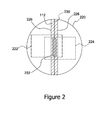
Figure 2 is an illustration of a field of view of an imaging device of the system ofFigure 1 , the field of view including a silicon rod; -
Figure 3 is the field of view shown inFigure 2 when the silicon rod has moved relative to the imaging device; -
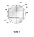
Figure 4 is the field of view shown inFigure 2 when the silicon rod has increased in size; -
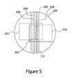
Figure 5 is an illustration of a field of view of an imaging device of the system ofFigure 1 , the field of view including two silicon rods overlapping within the field of view; and -
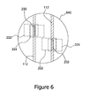
Figure 6 is an illustration of a field of view of an imaging device of the system ofFigure 1 , the field of view including two silicon rods. - Like reference symbols in the various drawings indicate like elements.
- The embodiments described herein generally relate to systems and methods for monitoring and controlling temperature in a polysilicon reactor. More specifically embodiments described herein relate to monitoring and controlling a silicon rod surface temperature using digital image analysis.
- A block diagram of an exemplary system, generally indicated by
reference numeral 100, according to the present disclosure is illustrated inFigure 1 .System 100 includes areactor 102 having a plurality ofsilicon rod groups 104. Apower supply 106 is coupled toreactor 102. More particularly,power supply 106 is coupled tosilicon rod groups 104.Power supply 106 includes acontroller 108 and amemory device 110.Imaging devices 116 are coupled toreactor 102, such as via a sight glass (not shown), to image one or more rod ofsilicon rod groups 104 and provide image data tocontroller 108. - In some embodiments,
reactor 102 is a chemical vapor deposition (CVD) reactor. More specifically, in some embodiments,reactor 102 is a Siemens reactor. In other embodiments,reactor 102 may be any other suitable polysilicon reactor. - In the illustrated embodiment, each
silicon rod group 104 includes a pair of series connectedsilicon rods 112. In other embodiments,silicon rod groups 104 may include any number of series connected silicon rods 112 (whether connected in pairs or not). In some embodiments, eachsilicon rod group 104 includes sixsilicon rods 112 connected in series. Current through the series connected silicon rods 112 (i.e., through each silicon rod group 104) is controlled to control the surface temperature ofsilicon rods 112.System 100 may include any suitable number ofsilicon rods 112, however configured and/or grouped. For example,system 100 may include 12, 18, 36, 48, 54, or 84 silicon rods. - In the exemplary embodiment,
power supply 106 includes a plurality ofpower converters 114. Eachpower converter 114 is coupled to output power to a differentsilicon rod group 104. In other embodiments,power supply 106 may include asingle power converter 114 coupled to two or more of the silicon rod groups 104 (including, in some embodiments, all silicon rod groups 104). In some embodiments,power supply 106 may use one or more silicon controlled rectifiers with phase control to adjust the output current to one or moresilicon rod groups 104. In some embodiments,power supply 106 may include an inverter with adjustable DC output to control the output current to one or moresilicon rod groups 104.Power converters 114 may have any suitable topology including, for example, buck, boost, flyback, forward, full-bridge, or a combination thereof. -
Controller 108 may be an analog controller, a digital controller, or a combination of analog and digital controllers/components. In embodiments in whichcontroller 108 is a digital controller,controller 108 may include a processor, computer, etc. Althoughcontroller 108 is illustrated withinpower supply 106 in theFigure 1 ,controller 108 may, additionally or alternatively, be external topower supply 106. For example, functions described as performed bycontroller 108 may be performed, completely or partially, by a separate controller, such as a system controller, for example. -
Memory device 110 is one or more devices that enable information such as executable instructions and/or other data to be stored and retrieved.Memory device 110 may include one or more computer readable media, such as, without limitation, dynamic random access memory (DRAM), static random access memory (SRAM), a solid state disk, and/or a hard disk.Memory device 110 may be configured to store, without limitation, computer-executable instructions, algorithms, results, and/or any other type of data. In some embodiments,memory device 110 is integrated incontroller 108. In other embodiments memory device is external tocontroller 108 and/orpower supply 106. - In the exemplary embodiment,
imaging devices 116 are digital cameras equipped with a charge-coupled device (CCD) sensor.Imaging devices 116 are used to measure the intensity of emitted radiation fromsilicon rods 112, as will be described in more detail below. Accordingly,imaging devices 116 may be any sensor configured to sense wavelengths ranging within the visible spectrum including, for example, complementary metal-oxide-semiconductor (CMOS) imaging devices. In still other embodiments,imaging devices 116 may be optical devices operable to sense different wavelengths including, for example, infrared wavelengths, ultraviolet wavelengths, etc. In the exemplary embodiment,imaging devices 116 are scan area cameras. In other embodiments, imaging devices may be linear cameras. Scan area cameras are focused on a two-dimensional target, generally a rectangle, whose dimensions are customizable. In embodiments including a linear camera, the target is generally a line of variable length. -
Controller 108 includes asignal analyzer 118 that converts the radiation intensity monitored by imagingdevices 116 into a temperature value. Although illustrated as part ofcontroller 108,signal analyzer 118 may be incorporated in a separate controller, such as a system controller, a stand-alone controller, a camera controller, etc., and/or may be incorporated inimaging devices 116. Furthermore, any number ofappropriate signal analyzers 118 may be utilized insystem 100.Signal analyzer 118 may include any suitable commercial software package for digital image analysis or may include custom designed algorithms and/or software. In the exemplary embodiment,signal analyzer 118 converts the signal of radiation intensity, received from animaging device 116, into a temperature measurement by comparison between the spectral response of theimaging device 116 aimed at one ormore silicon rods 112 and the spectral response of animaging device 116 aimed at a reference source of electromagnetic radiation at a known temperature. Such reference source may be a calibration black body whose temperature is accurately monitored. - The exemplary embodiment monitors and controls surface temperature of
silicon rods 112 groups inreactor 102 without relying on a pyrometer. Instead,power supply 106 uses a feedback control scheme based on radiation emitted bysilicon rods 112 as monitored by imagingdevices 116. -
Silicon rods 112 are installed insidereactor 102 prior to start up and are constantly heated up at a temperature ranging between about 980°C and about 1200°C via Joule heating.Silicon rods 112 act as resistors which dissipate electrical current into thermal energy. The intensity of the electrical current is adjusted by a feedback control scheme in order to maintain the desired set point of temperature. - As initially installed in
reactor 102,silicon rods 112, also referred to as "slim rods", are generally square or rectangular in cross-section with characteristic dimensions ranging between about 5 to about 15 millimeters. In other embodiments, silicon rods may have hollow cylindrical or long slab shapes. These initial slim rods serve as germs to start the deposition process. Depending on many parameters, including the fluid dynamics of the gases insidereactor 102 and the geometry of thesilicon rods 112,silicon rods 112 tend to oscillate in a range from a few millimeters to a few centimeters. This oscillation is commonly caused by shear stress exerted by the gases inreactor 102 on the surface of thesilicon rods 112. Such oscillations may cause a fixed target aimed by, for example, a pyrometer to fall off the surface ofsilicon rod 112 for a period of time until thesilicon rod 112 returns to its position of repose. The oscillating motion persists until the diameter of thesilicon rods 112 increases, the inertia of thesilicon rods 112 increases, and/or silicon deposits on top of a graphite chuck (not illustrated) in which eachsilicon rod 112 is inserted. In some embodiments, the transitory time, i.e. the time during whichsilicon rods 112 oscillate, may last for several hours depending on operating parameters ofreactor 102 and the deposition rate of silicon. Until the motion ofsilicon rods 112 ceases, the temperature measured at a fixed target location, such as with a pyrometer, may be inaccurate and the electrical power fed toreactor 102 may not be an optimal value. - Instead of using a fixed target,
imaging system 100 dynamically identifies a target area onsilicon rods 112. Referring toFigure 2 ,imaging device 116 has a field ofview 220. In this and the subsequent Figures,imaging device 116 is a scan area camera with arectangular target 232. InFigure 2 , one ofsilicon rods 112 is within field ofview 220. A temperature field ofsilicon rod 112 and its surroundings is identified usingimaging device 116 andsignal analyzer 118 as described herein. Two overlappingrectangular scan areas view 220, and accordingly within the temperature field, such thatsilicon rod 112 will be found within at least one ofscan areas silicon rod 112. - The vertical position of
scan areas imaging device 116 is mounted. Within the field of view ofimaging device 116 all possible vertical positions wheretarget 232 may be identified are suitable. The position oftarget 232 may vary along a vertical line of about few centimeters at most, which generally does not affect the accuracy of the temperature measurement. - Each
scan area imaging devices 116, also referred to as resolution, may determine the accuracy of temperature measurement according to the present disclosure. - To measure the temperature of
silicon rod 112, scanareas left edge 226 and a verticalright edge 228 ofsilicon rod 112. A location midway betweenleft edge 226 and right edge 228 (i.e., approximately halfway betweenleft edge 226 and right edge 228) is determined to be acenter 230 ofsilicon rod 112. Surface temperature ofsilicon rod 112 is determined within atarget area 232 centered ondetermined center 230 ofsilicon rod 112. Thus,target 232 will remain generally aligned with the actual center ofsilicon rod 112 despite any movement ofsilicon rod 112. Althoughtarget 232 is illustrated as a rectangular shape inFigure 2 ,target 232 may have any other suitable shape including, for example, round, oval, square, hexagonal, etc. Moreover, the location midway betweenleft edge 226 andright edge 228 is selected to approximate the center ofsilicon rod 112 and need not be the exact midpoint betweenleft edge 226 andright edge 228. - The
edges scan areas silicon rod 112, to a higher temperature, indicating the surface ofsilicon rod 112. A temperature threshold may be used to identify the transitions that indicate the location ofedges - To locate
edges left scan area 222 andright scan area 224 are analyzed. In particular,left scan area 222 is scanned from left to right. When a transition from a dark pixel (representing a low temperature) to a light pixel (representing a higher temperature) is located,left edge 226 ofsilicon rod 112 has been located. This process is repeated forright scan area 224, but scanning right to left to identifyright edge 228. - Once the spatial limits of
silicon rod 112 are established by locating left andright edges target 232 for temperature measurement is calculated as the midpoint betweenedges center 230. - This process of seeking
edges silicon rod 112 is performed repeatedly, and is suitably performed at a relatively high frequency. Thus, the position oftarget 232 is computed so that it is regularly adjusted to the motion ofsilicon rod 112 caused by shear stress exerted by the flowing gases. Generally, the more frequent theedges silicon rod 112. In some embodiments, the process is repeated at a higher frequency than the oscillations ofsilicon rod 112. In other embodiments, the time between each inspection foredges system 100. - Turning to
Figure 3 , there may be times when no transition may be detected in one ofscan areas silicon rod 112 exceeds the limits of theparticular scan area silicon rods 112 are prone to large excursions. In such cases,system 100 uses the last recorded position for the undetected edge. Thus, inFigure 3 ,right edge 228 ofsilicon rod 112 is outside ofscan area 224. When scanareas right edge 228, indicated bylast edge 334, is used to indicateright edge 228. Becauselast edge 334 does not align withright edge 228, the computedcenter 230 is not theactual center 336 ofsilicon rod 112.Center 230 is, however, close enough toactual center 336 that target 232 remains onsilicon rod 112 and relatively close toactual center 336. Thus, accurate temperature measurements may be achieved even during relatively large excursions ofsilicon rod 112. - As shown in
Figure 4 , after sufficient deposition has occurred, the diameter ofsilicon rods 112 has increased so that nearly the entire field ofview 220 ofimaging device 116 is occupied by the surface ofsilicon rod 112. More particularly,silicon rod 112 completely fills both scanningareas areas last edges 334 are used to indicate the location of right and leftedges center 230 is calculated andtarget 232 is placed based onlast edges 334. At this stage, tracking the target position is no longer necessary and the tracking described herein may cease. In the exemplary embodiment, when no transition from light to dark pixels, i.e., no edge, is located for one hundred seconds, thetarget 232 tracking algorithm may cease operating and enters a stand-by mode. In other embodiments, the amount of time without an observed transition may be any other suitable length of time. In still other embodiments, the tracking algorithm continues to operate without ceasing even though no transitions are observed. - In case of silicon rods which may overlap within the field of
view 220 ofimaging device 116, the methods described herein may still be utilized. In order to locateedges silicon rod 112, fine tuning of the temperature threshold value may be needed. As illustrated inFigure 5 ,silicon rod 112 overlaps asecond silicon rod 538 within field ofview 220. The transition from dark to light pixels atleft edge 226 is confined within a narrower range as compared to, for example, a field ofview 220 with asingle silicon rod 112, such as inFigures 2-4 .Silicon rod 538 is generally located at further distance fromimaging device 116 than therod 112. The measured temperature ofsilicon rod 538 is thus generally slightly lower thansilicon rod 112. By defining a threshold value which is closer to the temperature ofsilicon rod 112 in the foreground,silicon rod 538 in the background may be considered as part of a dark region. Thus, leftedge 226 may be detected based on the temperature difference betweensilicon rod 538 andsilicon rod 112. - Furthermore, the methods described herein may be used to monitor the temperature of
multiple silicon rods 112 within a single field of view of oneimaging device 112, whether overlapping or not.Figure 6 illustrates a field ofview 640 of onimaging device 116 in which twonon-overlapping silicon rods 112 are visible. In this embodiment, fourscan areas scan area 222 and oneright scan area 224 for eachsilicon rod 112. Thus, the surface temperature of twodifferent rods 112 within the field ofview 640 may be monitored. The number ofrods 112 that may be monitored within one field of view is not limited to two and the temperature of more orfewer rods 112 may be monitored by asingle imaging device 116. Ifsilicon rods 112 overlap, or oscillate to such an extent as to appear to overlap, the thresholds used for identifyingedges 226 and/or 228 may be adjusted as described above to account for the smaller observed temperature difference atedges 226 and/or 228. Further, eachscan area scan areas rod 112 may be the same or different. - An additional, or alternative, feature of
system 100 is the ability to quantify the diameter of thesilicon rods 112 being monitored. While seeking the target as described above, the positions of theedges rods 112 are computed. The difference between theedges particular silicon rod 112 being monitored. - Image based systems and monitoring and control methods as described herein may achieve superior results to some known methods. For example, more accurate temperature monitoring may be achieved by more accurately locating the silicon rods and sensing the temperature around the center of the silicon rods. More accurate temperature measurement may improve control of the deposition process, resulting in increased performance in terms of deposition rate and morphology. Furthermore, more accurate temperature measurement may result in reduced energy consumption. Furthermore, accurate measurements of the diameter of silicon rods may be obtained. Knowledge of the actual diameter of a silicon rod at any given time may improve control over the CVD process, improve energy efficiency, and/or improve the quality of the resulting silicon.
- Some embodiments involve the use of one or more electronic or computing devices. Such devices typically include a processor or controller, such as a general purpose central processing unit (CPU), a graphics processing unit (GPU), a microcontroller, a reduced instruction set computer (RISC) processor, an application specific integrated circuit (ASIC), a programmable logic circuit (PLC), and/or any other circuit or processor capable of executing the functions described herein. The methods described herein may be encoded as executable instructions embodied in a computer readable medium, including, without limitation, a storage device and/or a memory device. Such instructions, when executed by a processor, cause the processor to perform at least a portion of the methods described herein. The above examples are exemplary only, and thus are not intended to limit in any way the definition and/or meaning of the term processor.
- When introducing elements of the present invention or the embodiment(s) thereof, the articles "a", "an", "the" and "said" are intended to mean that there are one or more of the elements. The terms "comprising", "including" and "having" are intended to be inclusive and mean that there may be additional elements other than the listed elements.
Claims (15)
- A method of monitoring a surface temperature of at least one silicon rod in a chemical vapor deposition (CVD) reactor (102) during a CVD process, the method comprising:capturing an image of an interior of the CVD reactor, the image including a silicon rod (112);scanning the image to identify a left edge (226) of the silicon rod and a right edge (228) of the silicon rod;identifying a target area (232) midway between the left edge and the right edge; anddetermining a temperature of the silicon rod in the target area.
- A method according to Claim 1, wherein the capturing an image comprises capturing a digital image of the interior of the CVD reactor (102).
- A method according to Claim 2, wherein the scanning the image comprises analyzing individual pixels of the image to locate a transition from a lower temperature to a higher temperature.
- A method according to Claim 2, wherein capturing the digital image comprises capturing a digital image of a visible wavelength of radiation within the CVD reactor (102).
- A method according to Claim 1, wherein the determining a temperature of the silicon rod (112) in the target area (232) comprises comparing a radiation intensity of the silicon rod captured in the image to a radiation intensity of a reference image.
- A method according to Claim 1, further comprising:controlling a surface temperature of the silicon rod (112) based on the determined temperature of the silicon rod in the target area (232).
- A method according to Claim 6, wherein the controlling a surface temperature comprises utilizing the determined temperature as feedback for a power supply (106) coupled to provide electrical power to the silicon rod (112).
- A system (100) comprising:a chemical vapor deposition (CVD) reactor (102) including an interior;a plurality of silicon rods (112) coupled within the interior of the CVD reactor, wherein preferably the plurality of silicon rods (112) comprises twenty or more silicon rods;an imaging device (116) positioned to capture an image of the interior of the CVD reactor and at least one silicon rod of the plurality of silicon rods;a controller (108) configured to:scan the image to identify a left edge (226) of the silicon rod and a right edge (228) of the silicon rod;identify a target area (232) midway between the left edge and the right edge;determine a temperature of the silicon rod in the target area.
- A system (100) according to Claim 8, wherein the system further comprises a power supply (106) coupled to the silicon rod (112), the power supply providing electrical power to the silicon rod to control the temperature of the silicon rod, wherein the controller (108) is further configured to utilize the determined temperature as feedback for the power supply.
- A system (100) according to Claim 8, wherein the imaging device (116) comprises a digital imaging device.
- A system (100) according to Claim 10, wherein the controller (108) is configured to scan the image to identify a left edge (226) of the silicon rod and a right edge (228) of the silicon rod by analyzing individual pixels of the image to locate a transition from a lower temperature to a higher temperature.
- A system (100) according to Claim 10 or 11, wherein the digital imaging device (116) comprises a visible wavelength digital imaging device.
- A system according to any one of Claims 10 to 12 wherein the imaging device comprises a charge-coupled device (CCD) sensor.
- A system (100) according to Claim 8, wherein the controller (108) is configured to determine a temperature of the silicon rod (112) in the target area (232) by comparing a radiation intensity of the silicon rod captured in the image to a radiation intensity of a reference image.
- A system (100) according to Claim 8, wherein the controller (108) is configured to:utilize a previously identified left edge or right edge of the silicon rod as the identified left edge or right edge of the silicon rod (112) when the controller fails to identify the left edge (226) or right edge (228) of the silicon rod.
Applications Claiming Priority (2)
| Application Number | Priority Date | Filing Date | Title |
|---|---|---|---|
| US201161507405P | 2011-07-13 | 2011-07-13 | |
| PCT/EP2012/063599 WO2013007754A1 (en) | 2011-07-13 | 2012-07-11 | Methods and systems for monitoring and controlling silicon rod temperature |
Publications (2)
| Publication Number | Publication Date |
|---|---|
| EP2732067A1 EP2732067A1 (en) | 2014-05-21 |
| EP2732067B1 true EP2732067B1 (en) | 2016-01-06 |
Family
ID=46489249
Family Applications (1)
| Application Number | Title | Priority Date | Filing Date |
|---|---|---|---|
| EP12733512.3A Active EP2732067B1 (en) | 2011-07-13 | 2012-07-11 | Methods and systems for monitoring and controlling silicon rod temperature |
Country Status (5)
| Country | Link |
|---|---|
| US (1) | US9115423B2 (en) |
| EP (1) | EP2732067B1 (en) |
| KR (1) | KR102015678B1 (en) |
| CN (1) | CN103814149B (en) |
| WO (1) | WO2013007754A1 (en) |
Cited By (1)
| Publication number | Priority date | Publication date | Assignee | Title |
|---|---|---|---|---|
| WO2019110091A1 (en) | 2017-12-05 | 2019-06-13 | Wacker Chemie Ag | Method for determining a surface temperature |
Families Citing this family (5)
| Publication number | Priority date | Publication date | Assignee | Title |
|---|---|---|---|---|
| KR101651004B1 (en) * | 2014-09-24 | 2016-08-25 | 오씨아이 주식회사 | Method and apparatus for producing silicon |
| JP7598886B2 (en) * | 2019-06-11 | 2024-12-12 | ワッカー ケミー アクチエンゲゼルシャフト | Method for producing polycrystalline silicon |
| CN110182811A (en) * | 2019-06-12 | 2019-08-30 | 新疆协鑫新能源材料科技有限公司 | A kind of reduction furnace auxiliary imaging system and autocontrol method |
| US20220274839A1 (en) * | 2019-07-16 | 2022-09-01 | Wacker Chemie Ag | Method for producing polycrystalline silicon |
| CN113834585B (en) * | 2021-09-24 | 2024-04-05 | 中国恩菲工程技术有限公司 | Method, system, device, medium and electronic equipment for detecting silicon rod in reduction furnace |
Family Cites Families (9)
| Publication number | Priority date | Publication date | Assignee | Title |
|---|---|---|---|---|
| US4659421A (en) | 1981-10-02 | 1987-04-21 | Energy Materials Corporation | System for growth of single crystal materials with extreme uniformity in their structural and electrical properties |
| US6544333B2 (en) | 1997-12-15 | 2003-04-08 | Advanced Silicon Materials Llc | Chemical vapor deposition system for polycrystalline silicon rod production |
| JP5017989B2 (en) * | 2006-09-27 | 2012-09-05 | ソニー株式会社 | Imaging apparatus and imaging method |
| US8150242B2 (en) | 2008-10-31 | 2012-04-03 | Applied Materials, Inc. | Use of infrared camera for real-time temperature monitoring and control |
| DE102009010086B4 (en) | 2009-01-29 | 2013-04-11 | Centrotherm Sitec Gmbh | Arrangement and method for measuring the temperature and the thickness growth of silicon rods in a silicon deposition reactor |
| CN101597060B (en) * | 2009-06-27 | 2012-05-09 | 东方电气集团东方汽轮机有限公司 | Video monitoring device for polysilicon growth |
| US8507051B2 (en) | 2009-07-15 | 2013-08-13 | Mitsubishi Materials Corporation | Polycrystalline silicon producing method |
| CN101870471B (en) * | 2010-07-08 | 2012-06-13 | 江苏中能硅业科技发展有限公司 | High-efficiency large polycrystalline silicon reducing furnace |
| KR101048006B1 (en) * | 2010-09-01 | 2011-07-13 | (주)세미머티리얼즈 | Polysilicon Manufacturing Apparatus and Manufacturing Method |
-
2012
- 2012-07-06 US US13/543,226 patent/US9115423B2/en active Active
- 2012-07-11 EP EP12733512.3A patent/EP2732067B1/en active Active
- 2012-07-11 KR KR1020147003395A patent/KR102015678B1/en active Active
- 2012-07-11 WO PCT/EP2012/063599 patent/WO2013007754A1/en not_active Ceased
- 2012-07-11 CN CN201280044407.3A patent/CN103814149B/en active Active
Cited By (2)
| Publication number | Priority date | Publication date | Assignee | Title |
|---|---|---|---|---|
| WO2019110091A1 (en) | 2017-12-05 | 2019-06-13 | Wacker Chemie Ag | Method for determining a surface temperature |
| US11515184B2 (en) | 2017-12-05 | 2022-11-29 | Wacker Chemie Ag | Method for determining a surface temperature |
Also Published As
| Publication number | Publication date |
|---|---|
| EP2732067A1 (en) | 2014-05-21 |
| US9115423B2 (en) | 2015-08-25 |
| WO2013007754A1 (en) | 2013-01-17 |
| CN103814149B (en) | 2016-09-28 |
| CN103814149A (en) | 2014-05-21 |
| KR20140060284A (en) | 2014-05-19 |
| US20130017139A1 (en) | 2013-01-17 |
| KR102015678B1 (en) | 2019-08-28 |
Similar Documents
| Publication | Publication Date | Title |
|---|---|---|
| US9115423B2 (en) | Methods and systems for monitoring and controlling silicon rod temperature | |
| CN101506634B (en) | Method and device for measuring surface temperature of continuous casting slab | |
| US20160065848A1 (en) | Thermography for a thermal imaging camera | |
| CN103196564B (en) | Infrared thermal imaging temperature measuring method by correcting surface emissivity through image segmentation | |
| CN112281208B (en) | A kind of liquid port distance determination method, device and single crystal furnace | |
| US10890490B2 (en) | Thermography process for converting signal to temperature in a thermal imaging system | |
| CN102634632B (en) | System and method for detecting temperature of converter flame | |
| CN102410880A (en) | Infrared focal plane array blind pixel detection method based on integral time adjustment | |
| CN102795627B (en) | Multi-parameter online monitoring and optimizing control device and method of polycrystalline silicon reduction furnace | |
| TWI558489B (en) | Laser processing system using thermal radiation image and method thereof | |
| US9255846B1 (en) | Digital temperature determination using a radiometrically calibrated and a non-calibrated digital thermal imager | |
| KR102399202B1 (en) | How to determine the surface temperature | |
| KR20190132412A (en) | System and Method for Thermomechanical Monitoring of Photovoltaic Receiver | |
| KR20220156107A (en) | Spectral filtering system, apparatus and method | |
| JPS639843A (en) | Gas detection device | |
| CN120683611A (en) | A temperature and speed monitoring system for silicon carbide epitaxial equipment | |
| JPH06186085A (en) | Method and device for measuring temperature | |
| KR102908052B1 (en) | System, apparatus, and method for improved background correction and calibration of optical devices | |
| KR101630408B1 (en) | Scanning system and method thereof | |
| CN112665734B (en) | Temperature measurement method and device based on reference calibration | |
| CN108801467B (en) | Infrared panoramic imaging inspection control method and device | |
| KR101260058B1 (en) | An apparatus for measuring the thickness and measuring method | |
| KR101510267B1 (en) | Apparatus for controlling cooler and method for operating the same | |
| Schiewe | Monitoring High Temperatures in Industrial Applications: High‐dynamic infrared cameras for non‐contact temperature measurement from 300 to 3,000° C | |
| Junhong et al. | Error correction research of colorimetric temperature-measurement based on CCD |
Legal Events
| Date | Code | Title | Description |
|---|---|---|---|
| PUAI | Public reference made under article 153(3) epc to a published international application that has entered the european phase |
Free format text: ORIGINAL CODE: 0009012 |
|
| 17P | Request for examination filed |
Effective date: 20140113 |
|
| AK | Designated contracting states |
Kind code of ref document: A1 Designated state(s): AL AT BE BG CH CY CZ DE DK EE ES FI FR GB GR HR HU IE IS IT LI LT LU LV MC MK MT NL NO PL PT RO RS SE SI SK SM TR |
|
| DAX | Request for extension of the european patent (deleted) | ||
| REG | Reference to a national code |
Ref country code: DE Ref legal event code: R079 Ref document number: 602012013652 Country of ref document: DE Free format text: PREVIOUS MAIN CLASS: C23C0014000000 Ipc: C23C0016240000 |
|
| RIC1 | Information provided on ipc code assigned before grant |
Ipc: G05D 23/27 20060101AFI20150616BHEP |
|
| GRAP | Despatch of communication of intention to grant a patent |
Free format text: ORIGINAL CODE: EPIDOSNIGR1 |
|
| RIC1 | Information provided on ipc code assigned before grant |
Ipc: G05D 23/27 20060101ALI20150703BHEP Ipc: C01B 33/035 20060101ALI20150703BHEP Ipc: C23C 16/52 20060101ALI20150703BHEP Ipc: C23C 16/46 20060101ALI20150703BHEP Ipc: C23C 16/24 20060101AFI20150703BHEP |
|
| INTG | Intention to grant announced |
Effective date: 20150730 |
|
| GRAS | Grant fee paid |
Free format text: ORIGINAL CODE: EPIDOSNIGR3 |
|
| GRAA | (expected) grant |
Free format text: ORIGINAL CODE: 0009210 |
|
| AK | Designated contracting states |
Kind code of ref document: B1 Designated state(s): AL AT BE BG CH CY CZ DE DK EE ES FI FR GB GR HR HU IE IS IT LI LT LU LV MC MK MT NL NO PL PT RO RS SE SI SK SM TR |
|
| REG | Reference to a national code |
Ref country code: GB Ref legal event code: FG4D |
|
| REG | Reference to a national code |
Ref country code: CH Ref legal event code: EP |
|
| REG | Reference to a national code |
Ref country code: IE Ref legal event code: FG4D |
|
| REG | Reference to a national code |
Ref country code: AT Ref legal event code: REF Ref document number: 768953 Country of ref document: AT Kind code of ref document: T Effective date: 20160215 |
|
| REG | Reference to a national code |
Ref country code: DE Ref legal event code: R096 Ref document number: 602012013652 Country of ref document: DE |
|
| REG | Reference to a national code |
Ref country code: LT Ref legal event code: MG4D |
|
| REG | Reference to a national code |
Ref country code: NL Ref legal event code: MP Effective date: 20160106 |
|
| REG | Reference to a national code |
Ref country code: AT Ref legal event code: MK05 Ref document number: 768953 Country of ref document: AT Kind code of ref document: T Effective date: 20160106 |
|
| PG25 | Lapsed in a contracting state [announced via postgrant information from national office to epo] |
Ref country code: NL Free format text: LAPSE BECAUSE OF FAILURE TO SUBMIT A TRANSLATION OF THE DESCRIPTION OR TO PAY THE FEE WITHIN THE PRESCRIBED TIME-LIMIT Effective date: 20160106 |
|
| PG25 | Lapsed in a contracting state [announced via postgrant information from national office to epo] |
Ref country code: FI Free format text: LAPSE BECAUSE OF FAILURE TO SUBMIT A TRANSLATION OF THE DESCRIPTION OR TO PAY THE FEE WITHIN THE PRESCRIBED TIME-LIMIT Effective date: 20160106 Ref country code: GR Free format text: LAPSE BECAUSE OF FAILURE TO SUBMIT A TRANSLATION OF THE DESCRIPTION OR TO PAY THE FEE WITHIN THE PRESCRIBED TIME-LIMIT Effective date: 20160407 Ref country code: HR Free format text: LAPSE BECAUSE OF FAILURE TO SUBMIT A TRANSLATION OF THE DESCRIPTION OR TO PAY THE FEE WITHIN THE PRESCRIBED TIME-LIMIT Effective date: 20160106 Ref country code: NO Free format text: LAPSE BECAUSE OF FAILURE TO SUBMIT A TRANSLATION OF THE DESCRIPTION OR TO PAY THE FEE WITHIN THE PRESCRIBED TIME-LIMIT Effective date: 20160406 Ref country code: ES Free format text: LAPSE BECAUSE OF FAILURE TO SUBMIT A TRANSLATION OF THE DESCRIPTION OR TO PAY THE FEE WITHIN THE PRESCRIBED TIME-LIMIT Effective date: 20160106 Ref country code: IT Free format text: LAPSE BECAUSE OF FAILURE TO SUBMIT A TRANSLATION OF THE DESCRIPTION OR TO PAY THE FEE WITHIN THE PRESCRIBED TIME-LIMIT Effective date: 20160106 |
|
| PG25 | Lapsed in a contracting state [announced via postgrant information from national office to epo] |
Ref country code: AT Free format text: LAPSE BECAUSE OF FAILURE TO SUBMIT A TRANSLATION OF THE DESCRIPTION OR TO PAY THE FEE WITHIN THE PRESCRIBED TIME-LIMIT Effective date: 20160106 Ref country code: LT Free format text: LAPSE BECAUSE OF FAILURE TO SUBMIT A TRANSLATION OF THE DESCRIPTION OR TO PAY THE FEE WITHIN THE PRESCRIBED TIME-LIMIT Effective date: 20160106 Ref country code: LV Free format text: LAPSE BECAUSE OF FAILURE TO SUBMIT A TRANSLATION OF THE DESCRIPTION OR TO PAY THE FEE WITHIN THE PRESCRIBED TIME-LIMIT Effective date: 20160106 Ref country code: PT Free format text: LAPSE BECAUSE OF FAILURE TO SUBMIT A TRANSLATION OF THE DESCRIPTION OR TO PAY THE FEE WITHIN THE PRESCRIBED TIME-LIMIT Effective date: 20160506 Ref country code: PL Free format text: LAPSE BECAUSE OF FAILURE TO SUBMIT A TRANSLATION OF THE DESCRIPTION OR TO PAY THE FEE WITHIN THE PRESCRIBED TIME-LIMIT Effective date: 20160106 Ref country code: SE Free format text: LAPSE BECAUSE OF FAILURE TO SUBMIT A TRANSLATION OF THE DESCRIPTION OR TO PAY THE FEE WITHIN THE PRESCRIBED TIME-LIMIT Effective date: 20160106 Ref country code: IS Free format text: LAPSE BECAUSE OF FAILURE TO SUBMIT A TRANSLATION OF THE DESCRIPTION OR TO PAY THE FEE WITHIN THE PRESCRIBED TIME-LIMIT Effective date: 20160506 Ref country code: RS Free format text: LAPSE BECAUSE OF FAILURE TO SUBMIT A TRANSLATION OF THE DESCRIPTION OR TO PAY THE FEE WITHIN THE PRESCRIBED TIME-LIMIT Effective date: 20160106 |
|
| REG | Reference to a national code |
Ref country code: DE Ref legal event code: R097 Ref document number: 602012013652 Country of ref document: DE |
|
| PG25 | Lapsed in a contracting state [announced via postgrant information from national office to epo] |
Ref country code: EE Free format text: LAPSE BECAUSE OF FAILURE TO SUBMIT A TRANSLATION OF THE DESCRIPTION OR TO PAY THE FEE WITHIN THE PRESCRIBED TIME-LIMIT Effective date: 20160106 Ref country code: DK Free format text: LAPSE BECAUSE OF FAILURE TO SUBMIT A TRANSLATION OF THE DESCRIPTION OR TO PAY THE FEE WITHIN THE PRESCRIBED TIME-LIMIT Effective date: 20160106 |
|
| PLBE | No opposition filed within time limit |
Free format text: ORIGINAL CODE: 0009261 |
|
| STAA | Information on the status of an ep patent application or granted ep patent |
Free format text: STATUS: NO OPPOSITION FILED WITHIN TIME LIMIT |
|
| PG25 | Lapsed in a contracting state [announced via postgrant information from national office to epo] |
Ref country code: RO Free format text: LAPSE BECAUSE OF FAILURE TO SUBMIT A TRANSLATION OF THE DESCRIPTION OR TO PAY THE FEE WITHIN THE PRESCRIBED TIME-LIMIT Effective date: 20160106 Ref country code: CZ Free format text: LAPSE BECAUSE OF FAILURE TO SUBMIT A TRANSLATION OF THE DESCRIPTION OR TO PAY THE FEE WITHIN THE PRESCRIBED TIME-LIMIT Effective date: 20160106 Ref country code: SM Free format text: LAPSE BECAUSE OF FAILURE TO SUBMIT A TRANSLATION OF THE DESCRIPTION OR TO PAY THE FEE WITHIN THE PRESCRIBED TIME-LIMIT Effective date: 20160106 Ref country code: SK Free format text: LAPSE BECAUSE OF FAILURE TO SUBMIT A TRANSLATION OF THE DESCRIPTION OR TO PAY THE FEE WITHIN THE PRESCRIBED TIME-LIMIT Effective date: 20160106 |
|
| 26N | No opposition filed |
Effective date: 20161007 |
|
| PG25 | Lapsed in a contracting state [announced via postgrant information from national office to epo] |
Ref country code: BE Free format text: LAPSE BECAUSE OF FAILURE TO SUBMIT A TRANSLATION OF THE DESCRIPTION OR TO PAY THE FEE WITHIN THE PRESCRIBED TIME-LIMIT Effective date: 20160106 |
|
| PG25 | Lapsed in a contracting state [announced via postgrant information from national office to epo] |
Ref country code: BG Free format text: LAPSE BECAUSE OF FAILURE TO SUBMIT A TRANSLATION OF THE DESCRIPTION OR TO PAY THE FEE WITHIN THE PRESCRIBED TIME-LIMIT Effective date: 20160406 Ref country code: SI Free format text: LAPSE BECAUSE OF FAILURE TO SUBMIT A TRANSLATION OF THE DESCRIPTION OR TO PAY THE FEE WITHIN THE PRESCRIBED TIME-LIMIT Effective date: 20160106 |
|
| REG | Reference to a national code |
Ref country code: CH Ref legal event code: PL |
|
| GBPC | Gb: european patent ceased through non-payment of renewal fee |
Effective date: 20160711 |
|
| PG25 | Lapsed in a contracting state [announced via postgrant information from national office to epo] |
Ref country code: MC Free format text: LAPSE BECAUSE OF FAILURE TO SUBMIT A TRANSLATION OF THE DESCRIPTION OR TO PAY THE FEE WITHIN THE PRESCRIBED TIME-LIMIT Effective date: 20160106 |
|
| PG25 | Lapsed in a contracting state [announced via postgrant information from national office to epo] |
Ref country code: CH Free format text: LAPSE BECAUSE OF NON-PAYMENT OF DUE FEES Effective date: 20160731 Ref country code: LI Free format text: LAPSE BECAUSE OF NON-PAYMENT OF DUE FEES Effective date: 20160731 Ref country code: FR Free format text: LAPSE BECAUSE OF NON-PAYMENT OF DUE FEES Effective date: 20160801 |
|
| REG | Reference to a national code |
Ref country code: FR Ref legal event code: ST Effective date: 20170331 |
|
| REG | Reference to a national code |
Ref country code: IE Ref legal event code: MM4A |
|
| PG25 | Lapsed in a contracting state [announced via postgrant information from national office to epo] |
Ref country code: GB Free format text: LAPSE BECAUSE OF NON-PAYMENT OF DUE FEES Effective date: 20160711 |
|
| PG25 | Lapsed in a contracting state [announced via postgrant information from national office to epo] |
Ref country code: IE Free format text: LAPSE BECAUSE OF NON-PAYMENT OF DUE FEES Effective date: 20160711 |
|
| PG25 | Lapsed in a contracting state [announced via postgrant information from national office to epo] |
Ref country code: LU Free format text: LAPSE BECAUSE OF NON-PAYMENT OF DUE FEES Effective date: 20160711 |
|
| PG25 | Lapsed in a contracting state [announced via postgrant information from national office to epo] |
Ref country code: HU Free format text: LAPSE BECAUSE OF FAILURE TO SUBMIT A TRANSLATION OF THE DESCRIPTION OR TO PAY THE FEE WITHIN THE PRESCRIBED TIME-LIMIT; INVALID AB INITIO Effective date: 20120711 Ref country code: CY Free format text: LAPSE BECAUSE OF FAILURE TO SUBMIT A TRANSLATION OF THE DESCRIPTION OR TO PAY THE FEE WITHIN THE PRESCRIBED TIME-LIMIT Effective date: 20160106 |
|
| PG25 | Lapsed in a contracting state [announced via postgrant information from national office to epo] |
Ref country code: MT Free format text: LAPSE BECAUSE OF NON-PAYMENT OF DUE FEES Effective date: 20160731 Ref country code: MK Free format text: LAPSE BECAUSE OF FAILURE TO SUBMIT A TRANSLATION OF THE DESCRIPTION OR TO PAY THE FEE WITHIN THE PRESCRIBED TIME-LIMIT Effective date: 20160106 |
|
| PG25 | Lapsed in a contracting state [announced via postgrant information from national office to epo] |
Ref country code: AL Free format text: LAPSE BECAUSE OF FAILURE TO SUBMIT A TRANSLATION OF THE DESCRIPTION OR TO PAY THE FEE WITHIN THE PRESCRIBED TIME-LIMIT Effective date: 20160106 Ref country code: TR Free format text: LAPSE BECAUSE OF FAILURE TO SUBMIT A TRANSLATION OF THE DESCRIPTION OR TO PAY THE FEE WITHIN THE PRESCRIBED TIME-LIMIT Effective date: 20160106 |
|
| REG | Reference to a national code |
Ref country code: DE Ref legal event code: R082 Ref document number: 602012013652 Country of ref document: DE Representative=s name: MAIWALD PATENTANWALTS- UND RECHTSANWALTSGESELL, DE Ref country code: DE Ref legal event code: R081 Ref document number: 602012013652 Country of ref document: DE Owner name: GLOBALWAFERS CO., LTD., TW Free format text: FORMER OWNER: MEMC ELECTRONIC MATERIALS S.P.A., NOVARA, IT |
|
| PGFP | Annual fee paid to national office [announced via postgrant information from national office to epo] |
Ref country code: DE Payment date: 20250729 Year of fee payment: 14 |