EP2731156A2 - Organic light emitting diode display - Google Patents
Organic light emitting diode display Download PDFInfo
- Publication number
- EP2731156A2 EP2731156A2 EP13173129.1A EP13173129A EP2731156A2 EP 2731156 A2 EP2731156 A2 EP 2731156A2 EP 13173129 A EP13173129 A EP 13173129A EP 2731156 A2 EP2731156 A2 EP 2731156A2
- Authority
- EP
- European Patent Office
- Prior art keywords
- layer
- emitting diode
- light emitting
- organic light
- high refractive
- Prior art date
- Legal status (The legal status is an assumption and is not a legal conclusion. Google has not performed a legal analysis and makes no representation as to the accuracy of the status listed.)
- Withdrawn
Links
Images




Classifications
-
- H—ELECTRICITY
- H10—SEMICONDUCTOR DEVICES; ELECTRIC SOLID-STATE DEVICES NOT OTHERWISE PROVIDED FOR
- H10K—ORGANIC ELECTRIC SOLID-STATE DEVICES
- H10K59/00—Integrated devices, or assemblies of multiple devices, comprising at least one organic light-emitting element covered by group H10K50/00
- H10K59/30—Devices specially adapted for multicolour light emission
- H10K59/38—Devices specially adapted for multicolour light emission comprising colour filters or colour changing media [CCM]
-
- H—ELECTRICITY
- H10—SEMICONDUCTOR DEVICES; ELECTRIC SOLID-STATE DEVICES NOT OTHERWISE PROVIDED FOR
- H10K—ORGANIC ELECTRIC SOLID-STATE DEVICES
- H10K59/00—Integrated devices, or assemblies of multiple devices, comprising at least one organic light-emitting element covered by group H10K50/00
- H10K59/80—Constructional details
- H10K59/875—Arrangements for extracting light from the devices
- H10K59/879—Arrangements for extracting light from the devices comprising refractive means, e.g. lenses
-
- H—ELECTRICITY
- H10—SEMICONDUCTOR DEVICES; ELECTRIC SOLID-STATE DEVICES NOT OTHERWISE PROVIDED FOR
- H10K—ORGANIC ELECTRIC SOLID-STATE DEVICES
- H10K50/00—Organic light-emitting devices
- H10K50/80—Constructional details
- H10K50/85—Arrangements for extracting light from the devices
- H10K50/858—Arrangements for extracting light from the devices comprising refractive means, e.g. lenses
-
- H—ELECTRICITY
- H10—SEMICONDUCTOR DEVICES; ELECTRIC SOLID-STATE DEVICES NOT OTHERWISE PROVIDED FOR
- H10K—ORGANIC ELECTRIC SOLID-STATE DEVICES
- H10K50/00—Organic light-emitting devices
- H10K50/80—Constructional details
- H10K50/86—Arrangements for improving contrast, e.g. preventing reflection of ambient light
- H10K50/865—Arrangements for improving contrast, e.g. preventing reflection of ambient light comprising light absorbing layers, e.g. light-blocking layers
-
- H—ELECTRICITY
- H10—SEMICONDUCTOR DEVICES; ELECTRIC SOLID-STATE DEVICES NOT OTHERWISE PROVIDED FOR
- H10K—ORGANIC ELECTRIC SOLID-STATE DEVICES
- H10K59/00—Integrated devices, or assemblies of multiple devices, comprising at least one organic light-emitting element covered by group H10K50/00
- H10K59/80—Constructional details
- H10K59/805—Electrodes
- H10K59/8051—Anodes
- H10K59/80518—Reflective anodes, e.g. ITO combined with thick metallic layers
-
- H—ELECTRICITY
- H10—SEMICONDUCTOR DEVICES; ELECTRIC SOLID-STATE DEVICES NOT OTHERWISE PROVIDED FOR
- H10K—ORGANIC ELECTRIC SOLID-STATE DEVICES
- H10K59/00—Integrated devices, or assemblies of multiple devices, comprising at least one organic light-emitting element covered by group H10K50/00
- H10K59/80—Constructional details
- H10K59/805—Electrodes
- H10K59/8052—Cathodes
- H10K59/80524—Transparent cathodes, e.g. comprising thin metal layers
-
- H—ELECTRICITY
- H10—SEMICONDUCTOR DEVICES; ELECTRIC SOLID-STATE DEVICES NOT OTHERWISE PROVIDED FOR
- H10K—ORGANIC ELECTRIC SOLID-STATE DEVICES
- H10K59/00—Integrated devices, or assemblies of multiple devices, comprising at least one organic light-emitting element covered by group H10K50/00
- H10K59/80—Constructional details
- H10K59/875—Arrangements for extracting light from the devices
- H10K59/878—Arrangements for extracting light from the devices comprising reflective means
-
- H—ELECTRICITY
- H10—SEMICONDUCTOR DEVICES; ELECTRIC SOLID-STATE DEVICES NOT OTHERWISE PROVIDED FOR
- H10K—ORGANIC ELECTRIC SOLID-STATE DEVICES
- H10K59/00—Integrated devices, or assemblies of multiple devices, comprising at least one organic light-emitting element covered by group H10K50/00
- H10K59/80—Constructional details
- H10K59/8791—Arrangements for improving contrast, e.g. preventing reflection of ambient light
- H10K59/8792—Arrangements for improving contrast, e.g. preventing reflection of ambient light comprising light absorbing layers, e.g. black layers
-
- H—ELECTRICITY
- H10—SEMICONDUCTOR DEVICES; ELECTRIC SOLID-STATE DEVICES NOT OTHERWISE PROVIDED FOR
- H10K—ORGANIC ELECTRIC SOLID-STATE DEVICES
- H10K50/00—Organic light-emitting devices
- H10K50/80—Constructional details
- H10K50/85—Arrangements for extracting light from the devices
- H10K50/856—Arrangements for extracting light from the devices comprising reflective means
-
- H—ELECTRICITY
- H10—SEMICONDUCTOR DEVICES; ELECTRIC SOLID-STATE DEVICES NOT OTHERWISE PROVIDED FOR
- H10K—ORGANIC ELECTRIC SOLID-STATE DEVICES
- H10K59/00—Integrated devices, or assemblies of multiple devices, comprising at least one organic light-emitting element covered by group H10K50/00
- H10K59/10—OLED displays
- H10K59/12—Active-matrix OLED [AMOLED] displays
- H10K59/122—Pixel-defining structures or layers, e.g. banks
Definitions
- a display device is a device for displaying an image, and currently, an organic light emitting diode display is receiving attention.
- a conventional organic light emitting diode (OLED) display includes an organic light emitting diode for emitting light for displaying an image.
- Embodiments may be realized by providing an organic light emitting diode display that includes a first substrate, an organic light emitting diode provided on the first substrate, a second substrate provided on the organic light emitting diode, and a capping layer provided between the second substrate and the organic light emitting diode.
- the capping layer collects light emitted by the organic light emitting diode in a direction of the second substrate corresponding to the organic light emitting diode.
- the second substrate includes a plurality of color filters, and a black matrix provided between the color filters.
- the capping layer collects the light that is irradiated in a direction away from the color filter from the organic emission layer in the direction of the color filter.
- the organic light emitting diode may include a first electrode provided on the first substrate, an organic emission layer that is provided on the first electrode and that emits the light, and a second electrode provided on the organic emission layer.
- the capping layer may collect the light that is irradiated in a direction away from the first electrode from the organic emission layer in the direction of the second substrate corresponding to the first electrode.
- the first electrode may be a light reflective electrode, and the second electrode may be a light transmissive electrode. There may be a plurality of first electrodes, and the plurality of first electrodes may be separated from each other. Each of the first electrodes may correspond to a respective one of the color filters.
- the organic emission layer may emit white light.
- the color filters may include a first color filter having a first color, a second color filter separated from the first color filter with the black matrix there between and having a second color, and a third color filter separated from the second color filter with the black matrix there between and having a third color.
- the capping layer preferably includes at least a high refractive material and a low refractive material, the high refractive material being in contact with the color filters and having a greater refractive index than the low refractive material.
- the capping layer may include a plurality of high refractive patterns separated from each other and corresponding to the first electrodes, and a low refractive pattern provided between neighboring high refractive patterns.
- the low refractive pattern may contact the high refractive pattern.
- the high refractive pattern may have a greater refractive index than the low refractive pattern.
- the high refractive pattern may have an inversely tapered end surface.
- the capping layer may include a high refractive layer separated from the organic light emitting diode and contacting the second substrate.
- the capping layer may further include an air layer formed between the high refractive layer and the organic light emitting diode.
- the capping layer may further include an intermediate refractive layer provided between the high refractive layer and the air layer.
- the intermediate refractive layer may contact the high refractive layer and the air layer.
- the intermediate refractive layer may have a refractive index between the refractive index of the high refractive layer and the refractive index of the air layer.
- the capping layer may further include a low refractive layer provided between the high refractive layer and the organic light emitting diode.
- the low refractive layer may contact the high refractive layer and the organic light emitting diode.
- the low refractive layer may have a lower refractive index than the high refractive layer.
- the capping layer may further include an intermediate refractive layer provided between the high refractive layer and the low refractive layer.
- the intermediate refractive layer may contact the high refractive layer and the low refractive layer.
- the intermediate refractive layer may have a refractive index between the refractive index of the high refractive layer and the refractive index of the low refractive layer.
- FIG. 1 shows a cross-sectional view of an organic light emitting diode (OLED) display according to an exemplary embodiment.
- OLED organic light emitting diode
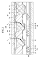
- FIG. 2 shows a cross-sectional view of a part A of FIG. 1 .
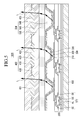
- FIG. 3 shows a cross-sectional view of a part of an organic light emitting diode (OLED) display according to a second exemplary embodiment.
- OLED organic light emitting diode
- FIG. 4 shows a cross-sectional view of a part of an organic light emitting diode (OLED) display according to a third exemplary embodiment.
- FIG. 5 shows a cross-sectional view of a part of an organic light emitting diode (OLED) display according to a fourth exemplary embodiment.
- FIG. 6 shows a cross-sectional view of a part of an organic light emitting diode (OLED) display according to a fifth exemplary embodiment.
- OLED organic light emitting diode
- FIG. 1 shows a cross-sectional view of an organic light emitting diode (OLED) display according to a first exemplary embodiment.
- FIG. 2 shows a cross-sectional view of a part A of FIG. 1 .
- the organic light emitting diode (OLED) display 1000 includes a first substrate 100, a wire unit 200, an organic light emitting diode 300, a second substrate 400, and a capping layer 500.
- the first substrate 100 may be an insulating substrate including, e.g., glass, a polymer, or stainless steel.
- the wire unit 200, the organic light emitting diode 300, and the capping layer 500 are provided on the first substrate 100.
- the first substrate 100 faces the second substrate 400 with the wire unit 200, the organic light emitting diode 300, and the capping layer 500 there between.
- the first substrate 100 may be bonded and sealed with the second substrate 400 by a sealant with the organic light emitting diode 300 there between.
- the first substrate 100 together with the second substrate 400 protects the wire unit 200 and the organic light emitting diode 300 from external interference.
- the wire unit 200 includes a switching thin film transistor (not shown) and a drive thin film transistor (TFT), and transmits a signal to the organic light emitting diode 300 to drive the organic light emitting diode 300.
- the organic light emitting diode 300 emits light according to the signal transmitted by the wire unit 200.
- the organic light emitting diode 300 is provided on the wire unit 200.
- the wire unit 200 and the organic light emitting diode 300 can be formed with various configurations within the range in which a skilled person can easily change or realize them.
- a drive thin film transistor (TFT) is shown for the wire unit 200
- the wire unit 200 can be a 2Tr-1Cap active matrix (AM) type of wire unit 200 having two thin film transistors (TFT) and one capacitor per pixel.
- Embodiments of the wire unit 200 are not limited by way of a number of thin film transistors, capacitors, and wires, etc.
- the pixel represents a minimum unit for displaying an image, and the organic light emitting diode (OLED) display displays the image through a plurality of pixels.
- the wire unit 200 can include a switching thin film transistor (not shown), a drive thin film transistor (TFT), and a capacitor (not shown) for each pixel.
- the wire unit 200 can further include a gate line disposed in a first direction of the first substrate 100, and a data line and a drive power line crossing the gate line in an insulated manner.
- One pixel can be defined by edges of the gate line, the data line, and the drive power line, but is not limited thereto.
- the switching thin film transistor includes a switching active layer, a switching gate electrode, a switching source electrode, and a switching drain electrode.
- the drive thin film transistor includes a drive active layer (AL), a drive gate electrode (GE), a drive source electrode (SE), and a drive drain electrode (DE).
- At least one of the drive active layer (AL) and the switching active layer can be formed with polysilicon or an oxide semiconductor.
- the oxide semiconductor includes, e.g., an oxide that is made based on zinc (Zn), gallium (Ga), tin (Sn), or indium (In), or complex oxides thereof such as zinc oxide (ZnO), indium-gallium-zinc oxide (InGaZnO 4 ), indium-zinc oxide (Zn-In-O), or zinc-tin oxide (Zn-Sn-O).
- the drive active layer (AL) and the switching active layer include a channel region to which an impurity is not doped, and a source region and a drain region that are formed when an impurity is doped on both sides of the channel region.
- the impurity is variable depending on a type of the thin film transistor, and an N-type impurity or a P-type impurity is usable.
- an additional protection layer can be added to at least one of the drive active layer (AL) and the switching active layer so as to protect the oxide semiconductor that is weak against external factors such as a high temperature.
- the switching thin film transistor is used as a switch for selecting a pixel to emit light, and the drive thin film transistor (TFT) applies drive power for emitting the organic emission layer 320 of the organic light emitting diode 300 in the selected pixel to the first electrode 310.
- TFT drive thin film transistor
- the organic light emitting diode 300 includes a first electrode 310, a second electrode 330 facing the first electrode 310, and an organic emission layer 320 provided between the first electrode 310 and the second electrode 330.
- the first electrode 310, the organic emission layer 320, and the second electrode 330 are sequentially stacked from the first substrate 100.
- the organic emission layer 320 is provided on the first electrode 310, and the second electrode 330 is provided on the organic emission layer 320.
- the first electrode 310 is provided on the first substrate 100.
- the first electrode 310 is, e.g., a hole injection electrode, an anode, and is a light reflective electrode.
- the first electrode 310 can include at least one conductive layer.
- the first electrode 310 can include a single-layer or multi-layered conductive layer including at least one of indium tin oxide (ITO), indium zinc oxide (IZO), magnesium silver (MgAg), aluminum (Al), and silver (Ag).
- ITO indium tin oxide
- IZO indium zinc oxide
- MgAg magnesium silver
- Al aluminum
- silver silver
- the first electrode 310 may include a conductive material with a greater work function compared to the second electrode 320, e.g., when hole injection performance for the organic emission layer 320 becomes greater.
- first electrodes 310 There may be a plurality of first electrodes 310, and each of the first electrodes 310 is provided to correspond to one pixel.
- the first electrodes 310 may be excluded in regions outside individual pixels, e.g., in non-pixel areas between adjacent pixels. Accordingly, the first electrodes 310 may be separated and/or spaced apart from each other, and may be disposed on the first substrate 100.
- the organic emission layer 320 may be formed with, e.g., a low molecular organic material or a polymer organic material such as poly3,4-ethylenedioxythiophene (PEDOT). Further, the organic emission layer 320 may be formed with a multilayer including at least one of an emission layer, a hole injection layer (HIL), a hole transport layer (HTL), an electron transport layer (ETL), and an electron injection layer (EIL). For example, when the organic emission layer 320 includes all of them, the hole injection layer (HIL) is disposed on the first electrode 310, and the hole transport layer (HTL), the emission layer, the electron transport layer (ETL), and the electron injection layer (EIL) are sequentially stacked thereon.
- the organic emission layer 320 emits white light when a red emission layer, a green emission layer, and a blue emission layer are sequentially stacked or when a white emission layer for emitting white light is stacked.
- the second electrode 330 is provided on the organic emission layer 320.
- the second electrode 330 is, e.g., an electron injection electrode, a cathode, and is a light transmissive electrode.
- the second electrode 330 is provided on the first substrate 100 to cover a plurality of first electrodes 310.
- the second electrode 330 includes at least one conductive layer.
- the second electrode 330 can include a single-layered or multi-layered conductive layer including at least one of indium tin oxide (ITO), indium zinc oxide (IZO), magnesium silver (MgAg), aluminum (Al), and silver (Ag).
- the second electrode 330 may include a conductive material with a low work function compared to the first electrode 310, e.g., so as to increase the electron injection performance for the organic emission layer 320.
- the organic light emitting diode 300 emits light in the direction of the second substrate 400. That is, the organic light emitting diode (OLED) display 1000 is a front light emitting type.
- the second substrate 400 is provided on the organic light emitting diode 300, and includes a second substrate main body 410, a color filter 420, and a black matrix 430.
- the second substrate main body 410 may be a light transmissive substrate including glass or a polymer.
- the color filters 420 may include a first color filter 421, a second color filter 422, and a third color filter 423.
- the first color filter 421 has a first color and converts white light emitted by the organic emission layer 320 into a first color light.
- the first color can be red.
- the second color filter 422 has a second color, and is separated from the first color filter 421 with the black matrix 430 there between.
- the second color filter 422 converts white light emitted by the organic emission layer 320 into a second color light.
- the second color can be green.
- the third color filter 423 has a third color and is separated from the second color filter 422 with the black matrix 430 there between.
- the third color filter 423 converts white light emitted by the organic emission layer 320 into a third color light.
- the third color can be blue. Accordingly, the first color, the second color, and the third color may be different from each other.
- the black matrix 430 is provided between the plurality of color filters 420.
- the black matrix 430 may reduce the possibility of and/or prevent the light emitted by the organic emission layer 320 from being output to a place where the color filter 420 is not provided.
- the capping layer 500 is provided between the second substrate 400 and the organic light emitting diode 300.
- the capping layer 500 may be directly between the organic light emitting diode 300 and the black matrix 430 and the plurality of color filters 420.
- the capping layer 500 which is provided between the second substrate 400 and the organic light emitting diode 300, collects white light emitted by the organic light emitting diode 300, e.g., collects white light emitted in the direction of the second substrate 400 corresponding to a location of the organic light emitting diode 300.
- the capping layer 500 collects the white light that is emitted by the organic emission layer 320 of the organic light emitting diode 300 and that is irradiated in a direction away from the color filter 420 corresponding to the first electrode 310, e.g., so as to orientate the light in the direction of the color filter 420 corresponding to the first electrode 310.
- the capping layer 500 includes, e.g., a plurality of high refractive patterns 510 and a plurality of low refractive patterns 520.
- the capping layer 500 may be formed as one continuous layer that includes the high refractive patterns 510 and the low refractive patterns 520 alternately arranged therein, e.g., along a cross section thereof.
- the high refractive patterns 510 may be formed spaced apart from each other, and the low refractive patterns 520 may form a continuous layer surrounding each of the high refractive patterns 510.
- the high refractive patterns 510 are separated from each other so as to be divided into portions that correspond to the plurality of first electrodes 310, e.g., each of the high refractive patterns may overlap one of the first electrodes 310.
- the high refractive patterns 510 may include an inversely tapered end surface 511.
- the high refractive pattern 510 has a greater refractive index than the low refractive pattern 520.
- the refractive index of the high refractive pattern 510 can be about 1.5 to about 1.8.
- the low refractive patterns 520 are provided between neighboring high refractive patterns 510, respectively, and contact the respective high refractive patterns 510.
- the high refractive pattern 510 and the low refractive pattern 520 respectively include one of an organic material and an inorganic material, and are selectively formed on the first substrate 100 or the second substrate 400.
- OLED organic light emitting diode
- Some light (L) of the white light emitted by the organic emission layer 320 of the organic light emitting diode (OLED) display 1000 is emitted by the organic emission layer 320 and is irradiated in the direction away from the color filter 420.
- This light (L) is reflected at an inversely tapered interface defined by the high refractive pattern 510 contacting the low refractive pattern 520 by a refractive index difference, and is collected in the direction of the color filter 420.
- luminous efficiency of the organic light emitting diode 300 is improved, and an amount of light (L) transmitting through the second substrate 400 from among the entire light emitted by the organic emission layer 320 is increased as the width of the color filter 420 can be formed more widely by considering a reflecting angle of the light (L), compared to the conventional color filter.
- the capping layer 500 including the high refractive pattern 510 and the low refractive pattern 520 is included, the luminous efficiency is improved and an aperture ratio is also improved to provide the organic light emitting diode (OLED) display 1000 having improved display quality.
- the capping layer 500 is provided between the second substrate 400 and the organic light emitting diode 300 so that the organic light emitting diode 300 is protected from external impact by the capping layer 500. That is, an organic light emitting diode (OLED) display 1000 with improved handling reliability is provided.
- OLED organic light emitting diode
- OLED organic light emitting diode
- FIG. 3 shows a cross-sectional view of a part of an organic light emitting diode (OLED) display according to a second exemplary embodiment.
- OLED organic light emitting diode
- a capping layer 502 of the organic light emitting diode (OLED) display 1002 includes a high refractive layer 530 and an air layer 540.
- the high refractive layer 530 is separated from the organic light emitting diode 300 and contacts the second substrate 400, and the air layer 540 is provided between, e.g., directly between, the high refractive layer 530 and the organic light emitting diode 300.
- the high refractive layer 530 has a greater refractive index than the air layer 540.
- the refractive index of the air layer 540 may be 1, and the refractive index of the high refractive layer 530 may be about 1.5 to about 1.8.
- the high refractive layer 530 includes at least one of an organic material and an inorganic material, and is formed on the second substrate 400.
- OLED organic light emitting diode
- Some light (L) of the white light emitted by the organic emission layer 320 of the organic light emitting diode (OLED) display 1002 is emitted by the organic emission layer 320 and is irradiated in the direction away from the color filter 420.
- This light (L) is refracted at an interface between the air layer 540 and the high refractive layer 530 by a refractive index difference and is collected in the direction of the color filter 420.
- luminous efficiency of the organic light emitting diode 300 is improved, and an amount of light (L) transmitting through the second substrate 400 from among the entire light emitted by the organic emission layer 320 is increased as the width of the color filter 420 can be formed more widely by considering a reflecting angle of the light (L), compared to the conventional color filter.
- the capping layer 502 including the high refractive layer 530 and the air layer 540 is included, the luminous efficiency is improved and an aperture ratio is also improved to provide the organic light emitting diode (OLED) display 1002 having improved display quality.
- OLED organic light emitting diode
- OLED organic light emitting diode
- FIG. 4 shows a cross-sectional view of a part of an organic light emitting diode (OLED) display 1003 according to a third exemplary embodiment.
- OLED organic light emitting diode
- a capping layer 503 of the organic light emitting diode (OLED) display 1003 includes a high refractive layer 530 and a low refractive layer 550.
- the high refractive layer 530 is separated from the organic light emitting diode 300 and contacts the second substrate 400, e.g., contacts the color filters 420.
- the low refractive layer 550 is provided between, e.g., directly between, the high refractive layer 530 and the organic light emitting diode 300.
- the low refractive layer 550 contacts the high refractive layer 530 and the organic light emitting diode 300.
- the high refractive layer 530 has a greater refractive index than the low refractive layer 550, and the low refractive layer 550 has a lesser refractive index than the high refractive layer 530.
- the refractive index of the low refractive layer 550 may be about 1.1 to about 1.4
- the refractive index of the high refractive layer 530 may be about 1.5 to about 1.8.
- the high refractive layer 530 and the low refractive layer 550 may include at least one of an organic material and an inorganic material, and may be selectively formed on the first substrate 100 or the second substrate 400.
- OLED organic light emitting diode
- Some light (L) of the white light emitted by the organic emission layer 320 of the organic light emitting diode (OLED) display 1003 is emitted by the organic emission layer 320 and is irradiated in the direction away from the color filter 420.
- This light (L) is refracted at an interface where the low refractive layer 550 and the high refractive layer 530 contact each other by a refractive index difference, and is collected in the direction of the color filter 420.
- luminous efficiency of the organic light emitting diode 300 is improved, and an amount of light (L) transmitting through the second substrate 400 from among the entire light emitted as the width of the color filter 420 can be formed more widely by considering a reflecting angle of the light (L), compared to the conventional color filter.
- the capping layer 503 comprising the high refractive layer 530 and the low refractive layer 550 is included, the luminous efficiency is improved and an aperture ratio is also improved to provide the organic light emitting diode (OLED) display 1003 having improved display quality.
- OLED organic light emitting diode
- OLED organic light emitting diode
- FIG. 5 shows a cross-sectional view of a part of an organic light emitting diode (OLED) 1004 display according to a fourth exemplary embodiment.
- OLED organic light emitting diode
- a capping layer 504 of the organic light emitting diode (OLED) display 1004 includes a high refractive layer 530, an air layer 540, and an intermediate refractive layer 560.
- the high refractive layer 530 is separated from the organic light emitting diode 300 and contacts the second substrate 400.
- the air layer 540 is formed between the high refractive layer 530 and the organic light emitting diode 300.
- the intermediate refractive layer 560 is provided between the high refractive layer 530 and the air layer 540, and contacts the high refractive layer 530 and the air layer 540, respectively.
- the high refractive layer 530 has a greater refractive index than the air layer 540
- the intermediate refractive layer 560 has a refractive index between the refractive index of the high refractive layer 530 and the refractive index of the air layer 540.
- the refractive index of the air layer 540 may be about 1
- the refractive index of the high refractive layer 530 may be about 1.5 to about 1.8
- the refractive index of the intermediate refractive layer 560 may be about 1.1 to about 1.4.
- the high refractive layer 530 and the intermediate refractive layer 560 may include at least one of an organic material and an inorganic material, and are sequentially stacked on the second substrate 400.
- OLED organic light emitting diode
- Some light (L) of the white light emitted by the organic emission layer 320 of the organic light emitting diode (OLED) display 1004 is emitted by the organic emission layer 320 and is irradiated in the direction away from the color filter 420.
- This light (L) is refracted at an interface where the air layer 540 and the intermediate refractive layer 560 contact each other and refracted again at an interface where the intermediate refractive layer 560 and the high refractive layer 530 contact each other by a refractive index difference, and is collected in the direction of the color filter 420.
- luminous efficiency of the organic light emitting diode 300 is improved, and an amount of light (L) transmitting through the second substrate 400 from among the entire light emitted by the organic emission layer 320 is increased as the width of the color filter 420 can be formed more widely by considering a reflecting angle of the light (L), compared to the conventional color filter.
- the capping layer 504 including the high refractive layer 530, the air layer 540, and the intermediate refractive layer 560 is included, the luminous efficiency is improved and an aperture ratio is also improved to provide the organic light emitting diode (OLED) display 1004 having improved display quality.
- OLED organic light emitting diode
- FIG. 6 shows a cross-sectional view of a part of an organic light emitting diode (OLED) display 1005 according to a fifth exemplary embodiment.
- OLED organic light emitting diode
- a capping layer 505 of the organic light emitting diode (OLED) display 1005 includes a high refractive layer 530, a low refractive layer 550, and an intermediate refractive layer 570.
- the high refractive layer 530 is separated from the organic light emitting diode 300 and contacts the second substrate 400.
- the low refractive layer 550 is provided between, e.g., directly between, the high refractive layer 530 and the organic light emitting diode 300.
- the intermediate refractive layer 570 is provided between the high refractive layer 530 and the low refractive layer 550, and contacts the high refractive layer 530 and the low refractive layer 550.
- the high refractive layer 530 has a greater refractive index than the low refractive layer 550.
- the intermediate refractive layer 570 has a refractive index between the refractive index of the high refractive layer 530 and the refractive index of the low refractive layer 550.
- the refractive index of the low refractive layer 550 may be about 1.1 to about 1.2
- the refractive index of the high refractive layer 530 may be about 1.5 to about 1.8
- the refractive index of the intermediate refractive layer 570 may be about 1.3 to about 1.4.
- the high refractive layer 530, the low refractive layer 550, and the intermediate refractive layer 570 respectively include at least one of an organic material and an inorganic material, and are selectively formed on the first substrate 100 or the second substrate 400.
- OLED organic light emitting diode
- Some light (L) of the white light emitted by the organic emission layer 320 of the organic light emitting diode (OLED) display 1005 is emitted by the organic emission layer 320 and is irradiated in the direction away from the color filter 420.
- This light (L) is refracted at an interface where the low refractive layer 550 and the intermediate refractive layer 570 contact each other and refracted again at an interface where the intermediate refractive layer 570 and the high refractive layer 530 contact each other, and is collected in the direction of the color filter 420.
- luminous efficiency of the organic light emitting diode 300 is improved, and an amount of light (L) transmitting through the second substrate 400 from among the entire light emitted by the organic emission layer 320 is increased by considering a reflecting angle of the light (L) and widening the color filter 420.
- the capping layer 505 including the high refractive layer 530, the low refractive layer 550, and the intermediate refractive layer 570 is included, the luminous efficiency is improved and an aperture ratio is also improved to provide the organic light emitting diode (OLED) display 1005 having improved display quality.
- a capping layer of an organic light emitting diode (OLED) display can further include an additional refractive layer between low refractive layers, intermediate refractive layers, and high refractive layers.
- an organic light emitting diode may include a first electrode, an organic emission layer, and a second electrode, which are sequentially stacked.
- an organic light emitting diode (OLED) display including an organic emission layer for emitting white light has been developed.
- a color filter may be positioned corresponding to the first electrode and the color filter modifies white light emitted by the organic emission layer into another color.
- a black matrix surrounding the color filters may be provided.
- the organic light emitting diode (OLED) display that includes the organic emission layer emitting white light may result in the white light digressing from the corresponding color filter. This white light may then be absorbed by the black matrix, thereby deteriorating overall luminous efficiency. Accordingly, embodiments relate to an organic light emitting diode (OLED) display that includes an organic light emitting diode for emitting white light such that an effort is made to provide improved luminous efficiency.
Landscapes
- Physics & Mathematics (AREA)
- Optics & Photonics (AREA)
- Electroluminescent Light Sources (AREA)
- Devices For Indicating Variable Information By Combining Individual Elements (AREA)
Abstract
Description
- A display device is a device for displaying an image, and currently, an organic light emitting diode display is receiving attention. A conventional organic light emitting diode (OLED) display includes an organic light emitting diode for emitting light for displaying an image.
- The above information disclosed in this Background section is only for enhancement of understanding of the background of the described technology and therefore it may contain information that does not form the prior art that is already known in this country to a person of ordinary skill in the art.
- Embodiments may be realized by providing an organic light emitting diode display that includes a first substrate, an organic light emitting diode provided on the first substrate, a second substrate provided on the organic light emitting diode, and a capping layer provided between the second substrate and the organic light emitting diode. The capping layer collects light emitted by the organic light emitting diode in a direction of the second substrate corresponding to the organic light emitting diode. The second substrate includes a plurality of color filters, and a black matrix provided between the color filters. The capping layer collects the light that is irradiated in a direction away from the color filter from the organic emission layer in the direction of the color filter.
- The organic light emitting diode may include a first electrode provided on the first substrate, an organic emission layer that is provided on the first electrode and that emits the light, and a second electrode provided on the organic emission layer. The capping layer may collect the light that is irradiated in a direction away from the first electrode from the organic emission layer in the direction of the second substrate corresponding to the first electrode.
- The first electrode may be a light reflective electrode, and the second electrode may be a light transmissive electrode. There may be a plurality of first electrodes, and the plurality of first electrodes may be separated from each other. Each of the first electrodes may correspond to a respective one of the color filters.
- The organic emission layer may emit white light.
- The color filters may include a first color filter having a first color, a second color filter separated from the first color filter with the black matrix there between and having a second color, and a third color filter separated from the second color filter with the black matrix there between and having a third color. The capping layer preferably includes at least a high refractive material and a low refractive material, the high refractive material being in contact with the color filters and having a greater refractive index than the low refractive material.
- The capping layer may include a plurality of high refractive patterns separated from each other and corresponding to the first electrodes, and a low refractive pattern provided between neighboring high refractive patterns. The low refractive pattern may contact the high refractive pattern. The high refractive pattern may have a greater refractive index than the low refractive pattern. The high refractive pattern may have an inversely tapered end surface.
- The capping layer may include a high refractive layer separated from the organic light emitting diode and contacting the second substrate. The capping layer may further include an air layer formed between the high refractive layer and the organic light emitting diode. The capping layer may further include an intermediate refractive layer provided between the high refractive layer and the air layer.
- The intermediate refractive layer may contact the high refractive layer and the air layer. The intermediate refractive layer may have a refractive index between the refractive index of the high refractive layer and the refractive index of the air layer. The capping layer may further include a low refractive layer provided between the high refractive layer and the organic light emitting diode.
- The low refractive layer may contact the high refractive layer and the organic light emitting diode. The low refractive layer may have a lower refractive index than the high refractive layer.
- The capping layer may further include an intermediate refractive layer provided between the high refractive layer and the low refractive layer. The intermediate refractive layer may contact the high refractive layer and the low refractive layer. The intermediate refractive layer may have a refractive index between the refractive index of the high refractive layer and the refractive index of the low refractive layer.
- Features will become apparent to those of ordinary skill in the art by describing in detail exemplary embodiments with reference to the attached drawings in which:
-
FIG. 1 shows a cross-sectional view of an organic light emitting diode (OLED) display according to an exemplary embodiment. -
FIG. 2 shows a cross-sectional view of a part A ofFIG. 1 . -
FIG. 3 shows a cross-sectional view of a part of an organic light emitting diode (OLED) display according to a second exemplary embodiment. -
FIG. 4 shows a cross-sectional view of a part of an organic light emitting diode (OLED) display according to a third exemplary embodiment. -
FIG. 5 shows a cross-sectional view of a part of an organic light emitting diode (OLED) display according to a fourth exemplary embodiment. -
FIG. 6 shows a cross-sectional view of a part of an organic light emitting diode (OLED) display according to a fifth exemplary embodiment. - Hereinafter, exemplary embodiments will be described in detail with reference to accompanying drawings so as to be easily understood by a person that is ordinary skilled in the art. As those skilled in the art would realize, the described embodiments may be modified in various different ways, all without departing from the scope of the present invention.
- Parts that are irrelevant to the description will be omitted to clearly describe the embodiments, and the same elements will be designated by the same reference numerals throughout the specification. Further, the size and thickness of each configuration shown in the drawings may be arbitrarily shown for understanding and ease of description, but the embodiments are not limited thereto.
- In the drawings, the thickness of layers, films, panels, regions, etc., are exaggerated for clarity. For understanding and ease of description, the thickness of some layers and areas is exaggerated. It will be understood that when an element such as a layer, film, region, or substrate is referred to as being "on" another element, it can be directly on the other element or intervening elements may also be present.
- In addition, unless explicitly described to the contrary, the word "comprise" and variations such as "comprises" or "comprising" will be understood to imply the inclusion of stated elements but not the exclusion of any other elements. The word "on" will be understood to be positioned above or below a target portion, and will not be necessarily understood to be positioned at an upper side based on a gravity direction.
- An organic light emitting diode (OLED) display according to a first exemplary embodiment will now be described with reference to
FIG. 1 andFIG. 2 . -
FIG. 1 shows a cross-sectional view of an organic light emitting diode (OLED) display according to a first exemplary embodiment.FIG. 2 shows a cross-sectional view of a part A ofFIG. 1 . - As shown in
FIG. 1 andFIG. 2 , the organic light emitting diode (OLED)display 1000 includes afirst substrate 100, awire unit 200, an organiclight emitting diode 300, asecond substrate 400, and acapping layer 500. - The
first substrate 100 may be an insulating substrate including, e.g., glass, a polymer, or stainless steel. Thewire unit 200, the organiclight emitting diode 300, and thecapping layer 500 are provided on thefirst substrate 100. Thefirst substrate 100 faces thesecond substrate 400 with thewire unit 200, the organiclight emitting diode 300, and thecapping layer 500 there between. Thefirst substrate 100 may be bonded and sealed with thesecond substrate 400 by a sealant with the organiclight emitting diode 300 there between. Thefirst substrate 100 together with thesecond substrate 400 protects thewire unit 200 and the organiclight emitting diode 300 from external interference. - The
wire unit 200 includes a switching thin film transistor (not shown) and a drive thin film transistor (TFT), and transmits a signal to the organiclight emitting diode 300 to drive the organiclight emitting diode 300. The organiclight emitting diode 300 emits light according to the signal transmitted by thewire unit 200. - The organic
light emitting diode 300 is provided on thewire unit 200. - Detailed configurations of the
wire unit 200 and the organiclight emitting diode 300 are shown inFIG. 2 , and embodiments are not restricted to the configuration ofFIG. 2 . Thewire unit 200 and the organiclight emitting diode 300 can be formed with various configurations within the range in which a skilled person can easily change or realize them. For example, in the drawing, for better understanding and ease of description, a drive thin film transistor (TFT) is shown for thewire unit 200, and thewire unit 200 can be a 2Tr-1Cap active matrix (AM) type ofwire unit 200 having two thin film transistors (TFT) and one capacitor per pixel. Embodiments of thewire unit 200 are not limited by way of a number of thin film transistors, capacitors, and wires, etc. The pixel represents a minimum unit for displaying an image, and the organic light emitting diode (OLED) display displays the image through a plurality of pixels. - For example, the
wire unit 200 can include a switching thin film transistor (not shown), a drive thin film transistor (TFT), and a capacitor (not shown) for each pixel. Thewire unit 200 can further include a gate line disposed in a first direction of thefirst substrate 100, and a data line and a drive power line crossing the gate line in an insulated manner. One pixel can be defined by edges of the gate line, the data line, and the drive power line, but is not limited thereto. - According to an exemplary embodiment, the switching thin film transistor includes a switching active layer, a switching gate electrode, a switching source electrode, and a switching drain electrode. The drive thin film transistor (TFT) includes a drive active layer (AL), a drive gate electrode (GE), a drive source electrode (SE), and a drive drain electrode (DE).
- At least one of the drive active layer (AL) and the switching active layer can be formed with polysilicon or an oxide semiconductor. The oxide semiconductor includes, e.g., an oxide that is made based on zinc (Zn), gallium (Ga), tin (Sn), or indium (In), or complex oxides thereof such as zinc oxide (ZnO), indium-gallium-zinc oxide (InGaZnO4), indium-zinc oxide (Zn-In-O), or zinc-tin oxide (Zn-Sn-O). The drive active layer (AL) and the switching active layer include a channel region to which an impurity is not doped, and a source region and a drain region that are formed when an impurity is doped on both sides of the channel region. For example, the impurity is variable depending on a type of the thin film transistor, and an N-type impurity or a P-type impurity is usable. When at least one of the drive active layer (AL) and the switching active layer is formed with an oxide semiconductor, an additional protection layer can be added to at least one of the drive active layer (AL) and the switching active layer so as to protect the oxide semiconductor that is weak against external factors such as a high temperature.
- The switching thin film transistor is used as a switch for selecting a pixel to emit light, and the drive thin film transistor (TFT) applies drive power for emitting the
organic emission layer 320 of the organiclight emitting diode 300 in the selected pixel to thefirst electrode 310. - The organic
light emitting diode 300 includes afirst electrode 310, asecond electrode 330 facing thefirst electrode 310, and anorganic emission layer 320 provided between thefirst electrode 310 and thesecond electrode 330. For example, thefirst electrode 310, theorganic emission layer 320, and thesecond electrode 330 are sequentially stacked from thefirst substrate 100. Theorganic emission layer 320 is provided on thefirst electrode 310, and thesecond electrode 330 is provided on theorganic emission layer 320. - The
first electrode 310 is provided on thefirst substrate 100. Thefirst electrode 310 is, e.g., a hole injection electrode, an anode, and is a light reflective electrode. Thefirst electrode 310 can include at least one conductive layer. For example, thefirst electrode 310 can include a single-layer or multi-layered conductive layer including at least one of indium tin oxide (ITO), indium zinc oxide (IZO), magnesium silver (MgAg), aluminum (Al), and silver (Ag). Thefirst electrode 310 may include a conductive material with a greater work function compared to thesecond electrode 320, e.g., when hole injection performance for theorganic emission layer 320 becomes greater. - There may be a plurality of
first electrodes 310, and each of thefirst electrodes 310 is provided to correspond to one pixel. For example, thefirst electrodes 310 may be excluded in regions outside individual pixels, e.g., in non-pixel areas between adjacent pixels. Accordingly, thefirst electrodes 310 may be separated and/or spaced apart from each other, and may be disposed on thefirst substrate 100. - The
organic emission layer 320 may be formed with, e.g., a low molecular organic material or a polymer organic material such as poly3,4-ethylenedioxythiophene (PEDOT). Further, theorganic emission layer 320 may be formed with a multilayer including at least one of an emission layer, a hole injection layer (HIL), a hole transport layer (HTL), an electron transport layer (ETL), and an electron injection layer (EIL). For example, when theorganic emission layer 320 includes all of them, the hole injection layer (HIL) is disposed on thefirst electrode 310, and the hole transport layer (HTL), the emission layer, the electron transport layer (ETL), and the electron injection layer (EIL) are sequentially stacked thereon. Theorganic emission layer 320 emits white light when a red emission layer, a green emission layer, and a blue emission layer are sequentially stacked or when a white emission layer for emitting white light is stacked. - The
second electrode 330 is provided on theorganic emission layer 320. Thesecond electrode 330 is, e.g., an electron injection electrode, a cathode, and is a light transmissive electrode. Thesecond electrode 330 is provided on thefirst substrate 100 to cover a plurality offirst electrodes 310. Thesecond electrode 330 includes at least one conductive layer. For example, thesecond electrode 330 can include a single-layered or multi-layered conductive layer including at least one of indium tin oxide (ITO), indium zinc oxide (IZO), magnesium silver (MgAg), aluminum (Al), and silver (Ag). Thesecond electrode 330 may include a conductive material with a low work function compared to thefirst electrode 310, e.g., so as to increase the electron injection performance for theorganic emission layer 320. - In the organic light emitting diode (OLED)
display 1000 according to the first exemplary embodiment, the organiclight emitting diode 300 emits light in the direction of thesecond substrate 400. That is, the organic light emitting diode (OLED)display 1000 is a front light emitting type. - The
second substrate 400 is provided on the organiclight emitting diode 300, and includes a second substratemain body 410, acolor filter 420, and ablack matrix 430. - The second substrate
main body 410 may be a light transmissive substrate including glass or a polymer. - There may be a plurality of
color filters 420 within thesecond substrate 400. The plurality ofcolor filters 420 are positioned corresponding to thefirst electrodes 310, respectively. For example, each of thecolor filters 420 may overlap one of thefirst electrodes 310, and a maximum width of thecolor filters 420 along a first direction may be substantially equal to a length of thefirst electrodes 310 along the first direction so as to completely overlap each other. The color filters 420 may include afirst color filter 421, asecond color filter 422, and athird color filter 423. - The
first color filter 421 has a first color and converts white light emitted by theorganic emission layer 320 into a first color light. For example, the first color can be red. - The
second color filter 422 has a second color, and is separated from thefirst color filter 421 with theblack matrix 430 there between. Thesecond color filter 422 converts white light emitted by theorganic emission layer 320 into a second color light. For example, the second color can be green. - The
third color filter 423 has a third color and is separated from thesecond color filter 422 with theblack matrix 430 there between. Thethird color filter 423 converts white light emitted by theorganic emission layer 320 into a third color light. For example, the third color can be blue. Accordingly, the first color, the second color, and the third color may be different from each other. - The
black matrix 430 is provided between the plurality ofcolor filters 420. Theblack matrix 430 may reduce the possibility of and/or prevent the light emitted by theorganic emission layer 320 from being output to a place where thecolor filter 420 is not provided. - The
capping layer 500 is provided between thesecond substrate 400 and the organiclight emitting diode 300. For example, thecapping layer 500 may be directly between the organiclight emitting diode 300 and theblack matrix 430 and the plurality ofcolor filters 420. - The
capping layer 500, which is provided between thesecond substrate 400 and the organiclight emitting diode 300, collects white light emitted by the organiclight emitting diode 300, e.g., collects white light emitted in the direction of thesecond substrate 400 corresponding to a location of the organiclight emitting diode 300. For example, thecapping layer 500 collects the white light that is emitted by theorganic emission layer 320 of the organiclight emitting diode 300 and that is irradiated in a direction away from thecolor filter 420 corresponding to thefirst electrode 310, e.g., so as to orientate the light in the direction of thecolor filter 420 corresponding to thefirst electrode 310. - The
capping layer 500 includes, e.g., a plurality of highrefractive patterns 510 and a plurality of lowrefractive patterns 520. For example, thecapping layer 500 may be formed as one continuous layer that includes the highrefractive patterns 510 and the lowrefractive patterns 520 alternately arranged therein, e.g., along a cross section thereof. In an implementation, the highrefractive patterns 510 may be formed spaced apart from each other, and the lowrefractive patterns 520 may form a continuous layer surrounding each of the highrefractive patterns 510. - The high
refractive patterns 510 are separated from each other so as to be divided into portions that correspond to the plurality offirst electrodes 310, e.g., each of the high refractive patterns may overlap one of thefirst electrodes 310. The highrefractive patterns 510 may include an inversely taperedend surface 511. The highrefractive pattern 510 has a greater refractive index than the lowrefractive pattern 520. The refractive index of the highrefractive pattern 510 can be about 1.5 to about 1.8. - The low
refractive patterns 520 are provided between neighboring highrefractive patterns 510, respectively, and contact the respective highrefractive patterns 510. - The high
refractive pattern 510 and the lowrefractive pattern 520 respectively include one of an organic material and an inorganic material, and are selectively formed on thefirst substrate 100 or thesecond substrate 400. - An effect of the organic light emitting diode (OLED)
display 1000 according to a first exemplary embodiment will now be described. - Some light (L) of the white light emitted by the
organic emission layer 320 of the organic light emitting diode (OLED)display 1000 is emitted by theorganic emission layer 320 and is irradiated in the direction away from thecolor filter 420. This light (L) is reflected at an inversely tapered interface defined by the highrefractive pattern 510 contacting the lowrefractive pattern 520 by a refractive index difference, and is collected in the direction of thecolor filter 420. - Therefore, luminous efficiency of the organic
light emitting diode 300 is improved, and an amount of light (L) transmitting through thesecond substrate 400 from among the entire light emitted by theorganic emission layer 320 is increased as the width of thecolor filter 420 can be formed more widely by considering a reflecting angle of the light (L), compared to the conventional color filter. - That is, since the
capping layer 500 including the highrefractive pattern 510 and the lowrefractive pattern 520 is included, the luminous efficiency is improved and an aperture ratio is also improved to provide the organic light emitting diode (OLED)display 1000 having improved display quality. - Further, the
capping layer 500 is provided between thesecond substrate 400 and the organiclight emitting diode 300 so that the organiclight emitting diode 300 is protected from external impact by thecapping layer 500. That is, an organic light emitting diode (OLED)display 1000 with improved handling reliability is provided. - An organic light emitting diode (OLED) display according to a second exemplary embodiment will now be described with reference to
FIG. 3 . - Hereinafter, only specific portions that are different from those of the first exemplary embodiment are extracted to be described, and an omitted portion of description thereof depends on the first exemplary embodiment. In addition, in the second exemplary embodiment, for better comprehension and ease of description, the same constituent elements are designated by the same reference numerals as the first exemplary embodiment.
-
FIG. 3 shows a cross-sectional view of a part of an organic light emitting diode (OLED) display according to a second exemplary embodiment. - As shown in
FIG. 3 , acapping layer 502 of the organic light emitting diode (OLED)display 1002 includes a highrefractive layer 530 and anair layer 540. - The high
refractive layer 530 is separated from the organiclight emitting diode 300 and contacts thesecond substrate 400, and theair layer 540 is provided between, e.g., directly between, the highrefractive layer 530 and the organiclight emitting diode 300. The highrefractive layer 530 has a greater refractive index than theair layer 540. For example, the refractive index of theair layer 540 may be 1, and the refractive index of the highrefractive layer 530 may be about 1.5 to about 1.8. - The high
refractive layer 530 includes at least one of an organic material and an inorganic material, and is formed on thesecond substrate 400. - An effect of the organic light emitting diode (OLED)
display 1002 according to the second exemplary embodiment will now be described. - Some light (L) of the white light emitted by the
organic emission layer 320 of the organic light emitting diode (OLED)display 1002 is emitted by theorganic emission layer 320 and is irradiated in the direction away from thecolor filter 420. This light (L) is refracted at an interface between theair layer 540 and the highrefractive layer 530 by a refractive index difference and is collected in the direction of thecolor filter 420. - Therefore, luminous efficiency of the organic
light emitting diode 300 is improved, and an amount of light (L) transmitting through thesecond substrate 400 from among the entire light emitted by theorganic emission layer 320 is increased as the width of thecolor filter 420 can be formed more widely by considering a reflecting angle of the light (L), compared to the conventional color filter. - For example, since the
capping layer 502 including the highrefractive layer 530 and theair layer 540 is included, the luminous efficiency is improved and an aperture ratio is also improved to provide the organic light emitting diode (OLED)display 1002 having improved display quality. - An organic light emitting diode (OLED) display according to a third exemplary embodiment will now be described with reference to
FIG. 4 . - Hereinafter, only specific portions that are different from those of the first exemplary embodiment are extracted to be described, and an omitted portion of description thereof depends on the first exemplary embodiment. In addition, in the third exemplary embodiment, for better comprehension and ease of description, the same constituent elements are designated by the same reference numerals as in the first exemplary embodiment.
-
FIG. 4 shows a cross-sectional view of a part of an organic light emitting diode (OLED)display 1003 according to a third exemplary embodiment. - As shown in
FIG. 4 , acapping layer 503 of the organic light emitting diode (OLED)display 1003 includes a highrefractive layer 530 and a lowrefractive layer 550. - The high
refractive layer 530 is separated from the organiclight emitting diode 300 and contacts thesecond substrate 400, e.g., contacts the color filters 420. The lowrefractive layer 550 is provided between, e.g., directly between, the highrefractive layer 530 and the organiclight emitting diode 300. The lowrefractive layer 550 contacts the highrefractive layer 530 and the organiclight emitting diode 300. The highrefractive layer 530 has a greater refractive index than the lowrefractive layer 550, and the lowrefractive layer 550 has a lesser refractive index than the highrefractive layer 530. For example, the refractive index of the lowrefractive layer 550 may be about 1.1 to about 1.4, and the refractive index of the highrefractive layer 530 may be about 1.5 to about 1.8. - The high
refractive layer 530 and the lowrefractive layer 550 may include at least one of an organic material and an inorganic material, and may be selectively formed on thefirst substrate 100 or thesecond substrate 400. - An effect of the organic light emitting diode (OLED)
display 1003 according to a third exemplary embodiment will now be described. - Some light (L) of the white light emitted by the
organic emission layer 320 of the organic light emitting diode (OLED)display 1003 is emitted by theorganic emission layer 320 and is irradiated in the direction away from thecolor filter 420. This light (L) is refracted at an interface where the lowrefractive layer 550 and the highrefractive layer 530 contact each other by a refractive index difference, and is collected in the direction of thecolor filter 420. - Therefore, luminous efficiency of the organic
light emitting diode 300 is improved, and an amount of light (L) transmitting through thesecond substrate 400 from among the entire light emitted as the width of thecolor filter 420 can be formed more widely by considering a reflecting angle of the light (L), compared to the conventional color filter. - That is, since the
capping layer 503 comprising the highrefractive layer 530 and the lowrefractive layer 550 is included, the luminous efficiency is improved and an aperture ratio is also improved to provide the organic light emitting diode (OLED)display 1003 having improved display quality. - An organic light emitting diode (OLED) display according to a fourth exemplary embodiment will now be described with reference to
FIG. 5 . - Hereinafter, only specific portions that are different from those of the first exemplary embodiment are extracted to be described, and an omitted portion of description thereof depends on the first exemplary embodiment. In addition, in the fourth exemplary embodiment, for better comprehension and ease of description, the same constituent elements are designated by the same reference numerals as in the first exemplary embodiment.
-
FIG. 5 shows a cross-sectional view of a part of an organic light emitting diode (OLED) 1004 display according to a fourth exemplary embodiment. - As shown in
FIG. 5 , acapping layer 504 of the organic light emitting diode (OLED)display 1004 includes a highrefractive layer 530, anair layer 540, and an intermediaterefractive layer 560. - The high
refractive layer 530 is separated from the organiclight emitting diode 300 and contacts thesecond substrate 400. Theair layer 540 is formed between the highrefractive layer 530 and the organiclight emitting diode 300. The intermediaterefractive layer 560 is provided between the highrefractive layer 530 and theair layer 540, and contacts the highrefractive layer 530 and theair layer 540, respectively. The highrefractive layer 530 has a greater refractive index than theair layer 540, and the intermediaterefractive layer 560 has a refractive index between the refractive index of the highrefractive layer 530 and the refractive index of theair layer 540. For example, the refractive index of theair layer 540 may be about 1, the refractive index of the highrefractive layer 530 may be about 1.5 to about 1.8, and the refractive index of the intermediaterefractive layer 560 may be about 1.1 to about 1.4. - The high
refractive layer 530 and the intermediaterefractive layer 560 may include at least one of an organic material and an inorganic material, and are sequentially stacked on thesecond substrate 400. - An effect of the organic light emitting diode (OLED)
display 1004 according to a fourth exemplary embodiment will now be described. - Some light (L) of the white light emitted by the
organic emission layer 320 of the organic light emitting diode (OLED)display 1004 is emitted by theorganic emission layer 320 and is irradiated in the direction away from thecolor filter 420. This light (L) is refracted at an interface where theair layer 540 and the intermediaterefractive layer 560 contact each other and refracted again at an interface where the intermediaterefractive layer 560 and the highrefractive layer 530 contact each other by a refractive index difference, and is collected in the direction of thecolor filter 420. - Therefore, luminous efficiency of the organic
light emitting diode 300 is improved, and an amount of light (L) transmitting through thesecond substrate 400 from among the entire light emitted by theorganic emission layer 320 is increased as the width of thecolor filter 420 can be formed more widely by considering a reflecting angle of the light (L), compared to the conventional color filter. - That is, since the
capping layer 504 including the highrefractive layer 530, theair layer 540, and the intermediaterefractive layer 560 is included, the luminous efficiency is improved and an aperture ratio is also improved to provide the organic light emitting diode (OLED)display 1004 having improved display quality. - An organic light emitting diode (OLED) display according to a fifth exemplary embodiment will now be described with reference to
FIG. 6 . - Hereinafter, only specific portions that are different from those of the first exemplary embodiment are extracted to be described, and an omitted portion of description thereof depends on the first exemplary embodiment. In addition, in the fifth exemplary embodiment, for better comprehension and ease of description, the same constituent elements are designated by the same reference numerals as in the first exemplary embodiment.
-
FIG. 6 shows a cross-sectional view of a part of an organic light emitting diode (OLED)display 1005 according to a fifth exemplary embodiment. - As shown in
FIG. 6 , acapping layer 505 of the organic light emitting diode (OLED)display 1005 includes a highrefractive layer 530, a lowrefractive layer 550, and an intermediaterefractive layer 570. - The high
refractive layer 530 is separated from the organiclight emitting diode 300 and contacts thesecond substrate 400. The lowrefractive layer 550 is provided between, e.g., directly between, the highrefractive layer 530 and the organiclight emitting diode 300. The intermediaterefractive layer 570 is provided between the highrefractive layer 530 and the lowrefractive layer 550, and contacts the highrefractive layer 530 and the lowrefractive layer 550. The highrefractive layer 530 has a greater refractive index than the lowrefractive layer 550. The intermediaterefractive layer 570 has a refractive index between the refractive index of the highrefractive layer 530 and the refractive index of the lowrefractive layer 550. For example, the refractive index of the lowrefractive layer 550 may be about 1.1 to about 1.2, the refractive index of the highrefractive layer 530 may be about 1.5 to about 1.8, and the refractive index of the intermediaterefractive layer 570 may be about 1.3 to about 1.4. - The high
refractive layer 530, the lowrefractive layer 550, and the intermediaterefractive layer 570 respectively include at least one of an organic material and an inorganic material, and are selectively formed on thefirst substrate 100 or thesecond substrate 400. - An effect of the organic light emitting diode (OLED)
display 1005 according to a fifth exemplary embodiment will now be described. - Some light (L) of the white light emitted by the
organic emission layer 320 of the organic light emitting diode (OLED)display 1005 is emitted by theorganic emission layer 320 and is irradiated in the direction away from thecolor filter 420. This light (L) is refracted at an interface where the lowrefractive layer 550 and the intermediaterefractive layer 570 contact each other and refracted again at an interface where the intermediaterefractive layer 570 and the highrefractive layer 530 contact each other, and is collected in the direction of thecolor filter 420. - Therefore, luminous efficiency of the organic
light emitting diode 300 is improved, and an amount of light (L) transmitting through thesecond substrate 400 from among the entire light emitted by theorganic emission layer 320 is increased by considering a reflecting angle of the light (L) and widening thecolor filter 420. - That is, since the
capping layer 505 including the highrefractive layer 530, the lowrefractive layer 550, and the intermediaterefractive layer 570 is included, the luminous efficiency is improved and an aperture ratio is also improved to provide the organic light emitting diode (OLED)display 1005 having improved display quality. - A capping layer of an organic light emitting diode (OLED) display according to another exemplary embodiment can further include an additional refractive layer between low refractive layers, intermediate refractive layers, and high refractive layers.
- By way of summation and review, an organic light emitting diode may include a first electrode, an organic emission layer, and a second electrode, which are sequentially stacked. Further, an organic light emitting diode (OLED) display including an organic emission layer for emitting white light has been developed. According to an embodiment in which the organic emission layer emits white light, a color filter may be positioned corresponding to the first electrode and the color filter modifies white light emitted by the organic emission layer into another color. Further, a black matrix surrounding the color filters may be provided.
- The organic light emitting diode (OLED) display that includes the organic emission layer emitting white light may result in the white light digressing from the corresponding color filter. This white light may then be absorbed by the black matrix, thereby deteriorating overall luminous efficiency. Accordingly, embodiments relate to an organic light emitting diode (OLED) display that includes an organic light emitting diode for emitting white light such that an effort is made to provide improved luminous efficiency.
- Example embodiments have been disclosed herein, and although specific terms are employed, they are used and are to be interpreted in a generic and descriptive sense only and not for purpose of limitation. In some instances, as would be apparent to one of ordinary skill in the art as of the filing of the present application, features, characteristics, and/or elements described in connection with a particular embodiment may be used singly or in combination with features, characteristics, and/or elements described in connection with other embodiments unless otherwise specifically indicated. Accordingly, it will be understood that various changes in form and details may be made without departing from the scope of the present invention as set forth in the following claims.
Claims (14)
- An organic light emitting diode display (1000, 1002, 1003, 1004, 1005), comprising:a first substrate (100);an organic light emitting diode (300) on the first substrate (100);a second substrate (400) on the organic light emitting diode (300), the second substrate including a plurality of color filters (420) for transmitting light emitted from the organic light emitting diode (300) and a black matrix (430) provided between the color filters (420); anda capping layer (500, 502, 503, 504, 505) between the second substrate (400) and the organic light emitting diode (300) for collecting light emitted from the organic light emitting diode (300) towards areas of the second substrate (400) corresponding to the color filters (420).
- The organic light emitting diode display of claim 1, wherein:the organic light emitting diode (300) includes:a first electrode (310) on the first substrate (100);an organic emission layer (320) located on the first electrode (310) and adapted to emit light; anda second electrode (330) on the organic emission layer (320),wherein the capping layer (500, 502, 503, 504, 505) is configured to collect the light irradiated by the organic emission layer (320) in a direction away from the color filter (420) corresponding to the organic emission layer (320) and to redirect the light in a direction of the second substrate (400) corresponding to the color filter (420).
- The organic light emitting diode display of claim 2, wherein the first electrode (310) is a light reflective electrode, and the second electrode (330) is a light transmissive electrode.
- The organic light emitting diode display of one of claims 2 and 3, wherein the first electrode (310) is one of a plurality of first electrodes (310), the plurality of first electrodes (310) being separated from each other and corresponding to the color filters (420).
- The organic light emitting diode display of one of claims 2 to 4, wherein:the organic emission layer is adapted to emit white light.
- The organic light emitting diode display of one of the preceding claims, wherein the color filters (420) includes:a first color filter (421) having a first color;a second color filter (422) separated from the first color filter (421) with the black matrix (430) there between, the second color filter (422) having a second color, anda third color filter (423) separated from the first color filter (421) and from the second color filter (422) with the black matrix (430) there between, the third color filter (423) having a third color.
- The organic light emitting diode display of one of the preceding claims, wherein the capping layer (500, 502, 503, 504, 505) includes at least a high refractive material and a low refractive material, the high refractive material being in contact with the color filters (420) and having a greater refractive index than the low refractive material.
- The organic light emitting diode display of one of the preceding claims, wherein the capping layer (502, 503, 504, 505) includes:a high refractive layer (530) comprising the high refractive material, the high refractive layer (530) being separated from the organic light emitting diode (300) and contacting the second substrate (400), anda low refractive layer (540, 550) comprising the low refractive material and being located between the high refractive layer (530) and the organic light emitting diode (300).
- The organic light emitting diode display of claim 8, wherein the low refractive layer (540) is an air layer between the high refractive layer (530) and the organic light emitting diode (300).
- The organic light emitting diode display of one of claims 8 and 9, wherein the capping layer (504, 505) further includes an intermediate refractive layer (560, 570) between the high refractive layer (530) and the low refractive layer (540, 550),
wherein the intermediate refractive layer (560, 570) contacts the high refractive layer (530) and the low refractive layer (540, 550). - The organic light emitting diode display of claim 10, wherein the intermediate refractive layer (560, 570) has a refractive index between a refractive index of the high refractive layer (530) and a refractive index of the low refractive layer (540, 550).
- The organic light emitting diode display of one of claims 2 to 7, wherein the capping layer (500) includes:a plurality of high refractive patterns (510) comprising the high refractive material, the high refractive patterns (510) being separated from each other and corresponding to the first electrodes (310); anda low refractive pattern (520) comprising the low refractive material, the low refractive pattern (520) being provided between neighboring high refractive patterns (510).
- The organic light emitting diode display of claim 12, wherein the low refractive pattern (520) contacts the high refractive patterns (510).
- The organic light emitting diode display of one of claims 12 and 13, wherein each of the plurality of the high refractive patterns (510) has an inversely tapered end surface.
Applications Claiming Priority (1)
| Application Number | Priority Date | Filing Date | Title |
|---|---|---|---|
| KR1020120125642A KR102051103B1 (en) | 2012-11-07 | 2012-11-07 | Organic light emitting diode display |
Publications (2)
| Publication Number | Publication Date |
|---|---|
| EP2731156A2 true EP2731156A2 (en) | 2014-05-14 |
| EP2731156A3 EP2731156A3 (en) | 2016-05-04 |
Family
ID=48746232
Family Applications (1)
| Application Number | Title | Priority Date | Filing Date |
|---|---|---|---|
| EP13173129.1A Withdrawn EP2731156A3 (en) | 2012-11-07 | 2013-06-21 | Organic light emitting diode display |
Country Status (6)
| Country | Link |
|---|---|
| US (1) | US8921840B2 (en) |
| EP (1) | EP2731156A3 (en) |
| JP (1) | JP6315889B2 (en) |
| KR (1) | KR102051103B1 (en) |
| CN (1) | CN103811521B (en) |
| TW (2) | TWI588988B (en) |
Cited By (3)
| Publication number | Priority date | Publication date | Assignee | Title |
|---|---|---|---|---|
| EP3496176A1 (en) * | 2017-12-05 | 2019-06-12 | LG Display Co., Ltd. | Electroluminescent display device |
| EP3654383A1 (en) * | 2018-11-19 | 2020-05-20 | Samsung Display Co., Ltd. | Display device |
| EP3703147A1 (en) * | 2019-02-07 | 2020-09-02 | Samsung Display Co., Ltd. | Organic light emitting display |
Families Citing this family (33)
| Publication number | Priority date | Publication date | Assignee | Title |
|---|---|---|---|---|
| US8664681B2 (en) * | 2012-07-06 | 2014-03-04 | Invensas Corporation | Parallel plate slot emission array |
| KR102136789B1 (en) * | 2014-06-17 | 2020-07-23 | 삼성디스플레이 주식회사 | Organic light emitting diode |
| KR20160034457A (en) * | 2014-09-19 | 2016-03-30 | 삼성디스플레이 주식회사 | Organic light emitting diode device |
| KR101788366B1 (en) | 2014-11-24 | 2017-10-20 | 삼성디스플레이 주식회사 | Organic light emitting diode display compring capping layer having high refractive index |
| CN104409659B (en) * | 2014-12-18 | 2017-02-22 | 上海天马有机发光显示技术有限公司 | Organic light emitting diode and manufacturing method thereof |
| KR102359349B1 (en) * | 2015-02-03 | 2022-02-07 | 삼성디스플레이 주식회사 | Organic light emitting diode display |
| KR102416470B1 (en) * | 2015-12-21 | 2022-07-04 | 엘지디스플레이 주식회사 | Display panel with luminance efficiency improvement, display device comprising thereof, and method of fabricating the display panel |
| KR101695652B1 (en) * | 2016-04-11 | 2017-01-12 | 엘지디스플레이 주식회사 | Organic light emitting display device and method for fabricating the same |
| KR102608954B1 (en) * | 2016-09-30 | 2023-12-05 | 삼성디스플레이 주식회사 | Display device |
| CN107689426B (en) * | 2017-09-30 | 2024-04-05 | 京东方科技集团股份有限公司 | Light emitting device, electronic device and manufacturing method of light emitting device |
| KR102521760B1 (en) * | 2017-10-31 | 2023-04-13 | 엘지디스플레이 주식회사 | Organic light emitting diodes display |
| KR102433274B1 (en) * | 2017-11-28 | 2022-08-18 | 삼성디스플레이 주식회사 | Organic light emitting display device |
| US11557703B2 (en) | 2017-12-21 | 2023-01-17 | Lumileds Llc | Light intensity adaptive LED sidewalls |
| KR102596066B1 (en) * | 2018-07-16 | 2023-11-01 | 삼성디스플레이 주식회사 | Display device and manufacturing method thereof |
| CN109148718B (en) * | 2018-08-20 | 2020-08-04 | 武汉华星光电半导体显示技术有限公司 | Organic light-emitting display panel and manufacturing method thereof |
| KR102602673B1 (en) | 2018-10-12 | 2023-11-17 | 삼성디스플레이 주식회사 | Display device and method of manufacturing the same |
| CN109524568B (en) * | 2018-12-10 | 2021-09-24 | 京东方科技集团股份有限公司 | Organic light emitting diode panel, method for producing the same, and display device |
| KR102635472B1 (en) * | 2018-12-21 | 2024-02-08 | 삼성디스플레이 주식회사 | Display device and manufacturing the same |
| KR102772252B1 (en) | 2018-12-31 | 2025-02-24 | 삼성디스플레이 주식회사 | Display device |
| KR102806841B1 (en) | 2019-01-24 | 2025-05-19 | 삼성전자주식회사 | Display device |
| CN109904347B (en) * | 2019-03-15 | 2020-07-31 | 京东方科技集团股份有限公司 | Light emitting device, method of manufacturing the same, and display apparatus |
| KR102818038B1 (en) | 2019-03-19 | 2025-06-12 | 삼성디스플레이 주식회사 | Electronic apparatus |
| KR102758041B1 (en) * | 2019-04-30 | 2025-01-23 | 삼성디스플레이 주식회사 | Display device |
| KR102806402B1 (en) * | 2019-05-02 | 2025-05-13 | 삼성디스플레이 주식회사 | Display device |
| JP7707924B2 (en) * | 2020-01-24 | 2025-07-15 | ソニーグループ株式会社 | Light-emitting device and display device |
| CN112215067B (en) * | 2020-09-09 | 2024-05-17 | 深圳供电局有限公司 | Protection action analysis method, device, electronic equipment and storage medium |
| KR102861108B1 (en) * | 2020-11-03 | 2025-09-17 | 삼성디스플레이 주식회사 | Display device |
| WO2022123431A1 (en) | 2020-12-07 | 2022-06-16 | Oti Lumionics Inc. | Patterning a conductive deposited layer using a nucleation inhibiting coating and an underlying metallic coating |
| CN113517414B (en) * | 2021-07-09 | 2022-05-31 | 武汉天马微电子有限公司 | Display panel and display device |
| CN114824137B (en) * | 2022-04-26 | 2025-09-05 | 合肥京东方卓印科技有限公司 | Color film substrate, display panel, display device, and method for manufacturing color film substrate |
| CN115715107A (en) * | 2022-11-24 | 2023-02-24 | 京东方科技集团股份有限公司 | Display panel, manufacturing method of display panel and display device |
| JPWO2024128206A1 (en) * | 2022-12-12 | 2024-06-20 | ||
| CN115933245A (en) * | 2022-12-27 | 2023-04-07 | 惠科股份有限公司 | display device |
Citations (1)
| Publication number | Priority date | Publication date | Assignee | Title |
|---|---|---|---|---|
| GB2417598A (en) * | 2002-03-25 | 2006-03-01 | Fuji Electric Holdings Co | Organic EL display |
Family Cites Families (43)
| Publication number | Priority date | Publication date | Assignee | Title |
|---|---|---|---|---|
| JP2838735B2 (en) * | 1991-07-05 | 1998-12-16 | 富士ゼロックス株式会社 | Image reading device |
| EP0575684A1 (en) * | 1992-06-22 | 1993-12-29 | International Business Machines Corporation | Decoupled optic and electronic confinement laser diode |
| KR950703164A (en) * | 1993-06-25 | 1995-08-23 | 에프.제이. 스미트 | Polarizing beam splitter and magneto-optic reading device using the same |
| US5801798A (en) * | 1996-12-23 | 1998-09-01 | Motorola, Inc. | Fast speed liquid crystal phase spatial light modulator for enchanced display resolution |
| US6982178B2 (en) * | 2002-06-10 | 2006-01-03 | E Ink Corporation | Components and methods for use in electro-optic displays |
| JP3962572B2 (en) * | 2001-10-30 | 2007-08-22 | 出光興産株式会社 | Organic electroluminescence light emitting device |
| WO2003050607A1 (en) * | 2001-12-13 | 2003-06-19 | E Ink Corporation | Electrophoretic electronic displays with films having a low index of refraction |
| US8169684B2 (en) * | 2002-09-30 | 2012-05-01 | Gentex Corporation | Vehicular rearview mirror elements and assemblies incorporating these elements |
| CN1685769B (en) * | 2003-06-13 | 2011-05-11 | 富士电机控股株式会社 | Organic el display |
| US20070090387A1 (en) * | 2004-03-29 | 2007-04-26 | Articulated Technologies, Llc | Solid state light sheet and encapsulated bare die semiconductor circuits |
| KR100819975B1 (en) | 2005-01-19 | 2008-04-07 | 후지 덴키 홀딩스 가부시키가이샤 | Organic EL display |
| US20060276024A1 (en) * | 2005-06-03 | 2006-12-07 | Jian Wang | Process for forming an electronic device including workpieces and a conductive member therebetween |
| KR20080025500A (en) * | 2006-09-18 | 2008-03-21 | 삼성전자주식회사 | Display device and manufacturing method |
| US7812523B2 (en) * | 2005-11-15 | 2010-10-12 | Samsung Electronics Co., Ltd. | Display device having an auxiliary electrode for improved common voltage and fabricating method thereof |
| US7791115B2 (en) * | 2005-11-29 | 2010-09-07 | Samsung Mobile Display Co., Ltd. | Organic light emitting display device |
| JP2007157404A (en) * | 2005-12-01 | 2007-06-21 | Seiko Epson Corp | Display device and electronic device |
| JP2007265869A (en) | 2006-03-29 | 2007-10-11 | Toppan Printing Co Ltd | Organic electroluminescence element and display device |
| KR101288427B1 (en) * | 2006-08-07 | 2013-08-07 | 삼성디스플레이 주식회사 | Display substrate and method for manufacturing thereof |
| KR100778514B1 (en) * | 2006-08-09 | 2007-11-22 | 삼성에스디아이 주식회사 | Organic light emitting display |
| WO2008121414A1 (en) | 2007-03-30 | 2008-10-09 | The Regents Of The University Of Michigan | Oled with improved light outcoupling |
| US8119204B2 (en) * | 2007-04-27 | 2012-02-21 | Semiconductor Energy Laboratory Co., Ltd. | Film formation method and method for manufacturing light-emitting device |
| US7990060B2 (en) * | 2007-05-31 | 2011-08-02 | Lg Display Co., Ltd. | Organic light emitting display device and method of manufacturing the same |
| US8136961B2 (en) * | 2007-11-28 | 2012-03-20 | Global Oled Technology Llc | Electro-luminescent area illumination device |
| JP2009151945A (en) * | 2007-12-18 | 2009-07-09 | Fuji Electric Holdings Co Ltd | Organic EL light emitting device and manufacturing method thereof |
| US7894116B2 (en) * | 2008-01-09 | 2011-02-22 | Seiko Epson Corporation | Electro-optical device and electronic apparatus |
| JP5024059B2 (en) * | 2008-01-09 | 2012-09-12 | セイコーエプソン株式会社 | Electro-optical device and electronic apparatus |
| KR100953658B1 (en) * | 2008-06-05 | 2010-04-20 | 삼성모바일디스플레이주식회사 | Organic light emitting display |
| KR101475299B1 (en) * | 2008-08-20 | 2014-12-23 | 삼성디스플레이 주식회사 | Liquid crystal display device and manufacturing method thereof |
| KR101473792B1 (en) * | 2008-11-20 | 2014-12-18 | 삼성디스플레이 주식회사 | Liquid crystal display device manufacturing method and liquid crystal display device therefor |
| JP2010271456A (en) * | 2009-05-20 | 2010-12-02 | Sony Corp | Display device and manufacturing method thereof |
| EP2452381A1 (en) * | 2009-07-06 | 2012-05-16 | Arkema, Inc. | Oled substrate consisting of transparent conductive oxide (tco) and anti-iridescent undercoat |
| KR101107160B1 (en) * | 2009-07-10 | 2012-01-25 | 삼성모바일디스플레이주식회사 | Organic light emitting display and manufacturing method thereof |
| JP2011076844A (en) * | 2009-09-30 | 2011-04-14 | Sumitomo Chemical Co Ltd | Light emitting device |
| KR20110058126A (en) * | 2009-11-25 | 2011-06-01 | 삼성모바일디스플레이주식회사 | Organic light emitting display |
| KR101244706B1 (en) * | 2009-12-01 | 2013-03-18 | 삼성디스플레이 주식회사 | Organic light emitting diode display |
| KR101777122B1 (en) * | 2010-09-15 | 2017-09-12 | 엘지디스플레이 주식회사 | Liquid crystal display device |
| US8541792B2 (en) * | 2010-10-15 | 2013-09-24 | Guardian Industries Corp. | Method of treating the surface of a soda lime silica glass substrate, surface-treated glass substrate, and device incorporating the same |
| US8547015B2 (en) * | 2010-10-20 | 2013-10-01 | 3M Innovative Properties Company | Light extraction films for organic light emitting devices (OLEDs) |
| WO2012063700A1 (en) * | 2010-11-11 | 2012-05-18 | シャープ株式会社 | Light diffusing plate, organic electroluminescent display device, and electronic apparatus |
| KR20120120710A (en) * | 2011-04-25 | 2012-11-02 | 삼성디스플레이 주식회사 | Display device and method for manufacturing the same |
| KR101900372B1 (en) * | 2011-07-19 | 2018-11-05 | 삼성디스플레이 주식회사 | Display device and method for manufacturing the same |
| KR101846411B1 (en) * | 2011-11-03 | 2018-04-09 | 삼성디스플레이 주식회사 | Liguid crystal display |
| KR101333138B1 (en) * | 2012-03-05 | 2013-11-26 | 삼성디스플레이 주식회사 | Method for preparing organic light emitting device, substrate for transiting of an inorganic film and organic light emitting device |
-
2012
- 2012-11-07 KR KR1020120125642A patent/KR102051103B1/en active Active
-
2013
- 2013-03-15 US US13/832,676 patent/US8921840B2/en active Active
- 2013-04-08 JP JP2013080252A patent/JP6315889B2/en active Active
- 2013-05-16 TW TW102117304A patent/TWI588988B/en active
- 2013-05-16 TW TW106114579A patent/TWI633659B/en active
- 2013-06-21 EP EP13173129.1A patent/EP2731156A3/en not_active Withdrawn
- 2013-07-04 CN CN201310280479.4A patent/CN103811521B/en active Active
Patent Citations (1)
| Publication number | Priority date | Publication date | Assignee | Title |
|---|---|---|---|---|
| GB2417598A (en) * | 2002-03-25 | 2006-03-01 | Fuji Electric Holdings Co | Organic EL display |
Cited By (7)
| Publication number | Priority date | Publication date | Assignee | Title |
|---|---|---|---|---|
| EP3496176A1 (en) * | 2017-12-05 | 2019-06-12 | LG Display Co., Ltd. | Electroluminescent display device |
| US10700140B2 (en) | 2017-12-05 | 2020-06-30 | Lg Display Co., Ltd. | Electroluminescent display device |
| EP3654383A1 (en) * | 2018-11-19 | 2020-05-20 | Samsung Display Co., Ltd. | Display device |
| US11342525B2 (en) | 2018-11-19 | 2022-05-24 | Samsung Display Co., Ltd. | Display device |
| EP3703147A1 (en) * | 2019-02-07 | 2020-09-02 | Samsung Display Co., Ltd. | Organic light emitting display |
| US11195884B2 (en) | 2019-02-07 | 2021-12-07 | Samsung Display Co., Ltd. | Organic light emitting display |
| US11818937B2 (en) | 2019-02-07 | 2023-11-14 | Samsung Display Co., Ltd. | Organic light emitting display |
Also Published As
| Publication number | Publication date |
|---|---|
| KR20140059372A (en) | 2014-05-16 |
| KR102051103B1 (en) | 2019-12-03 |
| CN103811521B (en) | 2018-03-27 |
| TWI633659B (en) | 2018-08-21 |
| CN103811521A (en) | 2014-05-21 |
| EP2731156A3 (en) | 2016-05-04 |
| TW201731093A (en) | 2017-09-01 |
| JP6315889B2 (en) | 2018-04-25 |
| TW201419516A (en) | 2014-05-16 |
| US8921840B2 (en) | 2014-12-30 |
| JP2014096346A (en) | 2014-05-22 |
| US20140124749A1 (en) | 2014-05-08 |
| TWI588988B (en) | 2017-06-21 |
Similar Documents
| Publication | Publication Date | Title |
|---|---|---|
| US8921840B2 (en) | Organic light emitting diode display | |
| US10978673B2 (en) | Display device and organic luminescent display device | |
| KR102639567B1 (en) | Display device | |
| US10541291B2 (en) | Organic light-emitting display device | |
| KR102273654B1 (en) | Organic light emitting diode display | |
| KR102060622B1 (en) | Organic light emitting diode display | |
| US8274090B2 (en) | Organic light-emitting display device | |
| TWI535329B (en) | Organic light emitting display device | |
| US8797239B2 (en) | Organic light-emitting display device | |
| KR102510397B1 (en) | Thin film transistor and display device comprising the same | |
| KR20150085668A (en) | Display apparatus reducing dead space | |
| US9559330B2 (en) | Organic light emitting diode display | |
| US9601720B2 (en) | Organic light emitting diode display | |
| KR20150016031A (en) | Organic light emitting display apparatus and method of manufacturing thereof | |
| US20170033170A1 (en) | Organic light emitting diode display | |
| US20150042634A1 (en) | Organic light emitting diode display | |
| KR102052073B1 (en) | Flat panel display device | |
| KR102110471B1 (en) | Organic light emitting diode display | |
| KR20220140073A (en) | Display device |
Legal Events
| Date | Code | Title | Description |
|---|---|---|---|
| PUAI | Public reference made under article 153(3) epc to a published international application that has entered the european phase |
Free format text: ORIGINAL CODE: 0009012 |
|
| 17P | Request for examination filed |
Effective date: 20130621 |
|
| AK | Designated contracting states |
Kind code of ref document: A2 Designated state(s): AL AT BE BG CH CY CZ DE DK EE ES FI FR GB GR HR HU IE IS IT LI LT LU LV MC MK MT NL NO PL PT RO RS SE SI SK SM TR |
|
| AX | Request for extension of the european patent |
Extension state: BA ME |
|
| RAP1 | Party data changed (applicant data changed or rights of an application transferred) |
Owner name: SAMSUNG DISPLAY CO., LTD. |
|
| PUAL | Search report despatched |
Free format text: ORIGINAL CODE: 0009013 |
|
| AK | Designated contracting states |
Kind code of ref document: A3 Designated state(s): AL AT BE BG CH CY CZ DE DK EE ES FI FR GB GR HR HU IE IS IT LI LT LU LV MC MK MT NL NO PL PT RO RS SE SI SK SM TR |
|
| AX | Request for extension of the european patent |
Extension state: BA ME |
|
| RIC1 | Information provided on ipc code assigned before grant |
Ipc: H01L 51/52 20060101AFI20160331BHEP Ipc: H01L 27/32 20060101ALI20160331BHEP |
|
| RIN1 | Information on inventor provided before grant (corrected) |
Inventor name: KIM, IL-NAM Inventor name: KIM, GEE-BUM Inventor name: BAEK, SOO-MIN Inventor name: PARK, WON-SANG Inventor name: KIM, MIN-WOO |
|
| R17P | Request for examination filed (corrected) |
Effective date: 20160606 |
|
| RBV | Designated contracting states (corrected) |
Designated state(s): AL AT BE BG CH CY CZ DE DK EE ES FI FR GB GR HR HU IE IS IT LI LT LU LV MC MK MT NL NO PL PT RO RS SE SI SK SM TR |
|
| STAA | Information on the status of an ep patent application or granted ep patent |
Free format text: STATUS: EXAMINATION IS IN PROGRESS |
|
| 17Q | First examination report despatched |
Effective date: 20180525 |
|
| STAA | Information on the status of an ep patent application or granted ep patent |
Free format text: STATUS: THE APPLICATION HAS BEEN WITHDRAWN |
|
| 18W | Application withdrawn |
Effective date: 20190628 |