EP2731154A2 - Circuit layout for organic transistors in series or parallel - Google Patents
Circuit layout for organic transistors in series or parallel Download PDFInfo
- Publication number
- EP2731154A2 EP2731154A2 EP20130192088 EP13192088A EP2731154A2 EP 2731154 A2 EP2731154 A2 EP 2731154A2 EP 20130192088 EP20130192088 EP 20130192088 EP 13192088 A EP13192088 A EP 13192088A EP 2731154 A2 EP2731154 A2 EP 2731154A2
- Authority
- EP
- European Patent Office
- Prior art keywords
- region
- source
- drain
- regions
- gate
- Prior art date
- Legal status (The legal status is an assumption and is not a legal conclusion. Google has not performed a legal analysis and makes no representation as to the accuracy of the status listed.)
- Granted
Links
Images




Classifications
-
- H—ELECTRICITY
- H10—SEMICONDUCTOR DEVICES; ELECTRIC SOLID-STATE DEVICES NOT OTHERWISE PROVIDED FOR
- H10K—ORGANIC ELECTRIC SOLID-STATE DEVICES
- H10K10/00—Organic devices specially adapted for rectifying, amplifying, oscillating or switching; Organic capacitors or resistors having potential barriers
- H10K10/40—Organic transistors
- H10K10/46—Field-effect transistors, e.g. organic thin-film transistors [OTFT]
- H10K10/462—Insulated gate field-effect transistors [IGFETs]
- H10K10/481—Insulated gate field-effect transistors [IGFETs] characterised by the gate conductors
- H10K10/482—Insulated gate field-effect transistors [IGFETs] characterised by the gate conductors the IGFET comprising multiple separately-addressable gate electrodes
-
- H—ELECTRICITY
- H10—SEMICONDUCTOR DEVICES; ELECTRIC SOLID-STATE DEVICES NOT OTHERWISE PROVIDED FOR
- H10D—INORGANIC ELECTRIC SEMICONDUCTOR DEVICES
- H10D30/00—Field-effect transistors [FET]
- H10D30/60—Insulated-gate field-effect transistors [IGFET]
- H10D30/67—Thin-film transistors [TFT]
- H10D30/6729—Thin-film transistors [TFT] characterised by the electrodes
- H10D30/673—Thin-film transistors [TFT] characterised by the electrodes characterised by the shapes, relative sizes or dispositions of the gate electrodes
- H10D30/6733—Multi-gate TFTs
Definitions
- the conventional structure of an individual thin-film transistor consists of two lateral electrodes for source and drain current collection or injection, modulated by a third gate electrode.
- the source and drain electrodes are usually conductors, such as silver, gold, copper, doped polymer, or conductive oxides such as indium tin oxide.
- TFT circuits are laid out by connecting individual TFTs and other elements with metal interconnect.
- a pair of unipolar (i.e., both n-type or both p-type) TFTs is typically realized by laying out two separate TFTs and wiring them together.
- the source of one TFT is wired to the drain of the other TFT with interconnect, generally formed in the drain or source metal layer.
- FIG. 1 is a top view of an exemplary stack of three thin film transistors arranged in series, with a metal layer in each source and drain region.
- FIG. 2 is a bottom view of FIG. 1 .
- FIG. 3 is a side view of FIG. 1 .
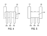
- FIG. 4 is a top view of an exemplary stack of three thin film transistors arranged in series, without metal layers in the intermediary source and drain regions.
- FIG. 5 is a bottom view of FIG. 4 .
- FIG. 6 is a side view of FIG. 4 .
- FIG. 7 is another side view of FIG. 4 , further illustrating intermediary source and drain regions without an accompanying metal layer.
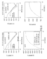
- FIG. 8 is an illustrative comparison of current according to embodiments of FIGS. 1-3 versus current according to embodiments of FIGS. 4-7
- FIG. 9 is an illustrative comparison of the resistivity of commercially available semiconductor according to embodiments.
- FIG. 10 is another embodiment of the structure of FIGS. 4-7 .
- FIG. 11 is a side view of an exemplary stack of three thin film transistors arranged in series, in bottom-gate orientation.
- FIG. 12 is a side view of FIG. 11 , without metal layers in the intermediary source and drain regions.
- FIG. 13 is an exemplary top view of a stack of three TFTs arranged in parallel.
- FIG. 14 is a bottom view of FIG. 13 .
- FIG. 15 is an exemplary top view of a transmission gate.
- the area of TFTs connected in series is greatly reduced in an embodiment of the invention.
- This technique is not limited to pairs of TFTs, but is applied to stacks of three or more TFTs. Additionally, the technique can be adapted to arrange TFTs in parallel by laying out two or more TFTs with their respective source regions and drain regions coinciding.
- source region 170 and drain region 180 terminate a series of source and drain terminals. Occupying a portion of source region 170 is a source conductor 110, and occupying a portion of drain region 180 is a drain conductor 120.
- Gate 150a is located between source region 170 and a drain region 175a that also doubles as a source region 175a for gate 150b.
- Metal layer 130a occupies a portion of the coinciding source/drain region 175a.
- the metal layer 130a serves as both a source and drain conductor, and may be substituted for other conductive materials, such as a conductive polymer, a metal oxide, or a doped semiconductor material.
- the conductive materials 130a and 130b may be of materials different than the materials of conductors 110 and 120.
- source or drain conductors may be affixed to points of contact on the semiconductor.
- Source region 175a and drain region 175b form the second of three TFTs with gate 150b.
- source region 175b and drain region 180 form the third of the three TFTs with gate 150c.
- Metal layer 130b occupies a portion of the source/drain region 175b.
- the gates 150a-c and dielectric 160 are of materials and dimensions such that a potential applied between the gate and any source or drain can induce depletion or enhancement of a channel or part of a channel between the source and drain regions. It is important to note that regions 175a and 175b occupy a dual role as both a source and drain for the multiplicity of transistors formed by the structure of Figures 1-3 .
- gates 150a-c are formed from a metallic conductor layered onto the dielectric 160 with a printing process.
- the metal layers 110, 130a, 130b, and 120 occupy a portion of the drain and source regions 170, 175a-b, and 180 are layered onto a substrate with a printing process.
- a semiconductor material such as solution blends of organic semiconductors, inorganic solgel, or nanoparticle dispersion is spread over the conductors of drain/source regions 170, 180, and 175a-b, which later forms a solid thin film.
- Dielectric material 160 then tops the semiconductor material 140, separating the gates 150a-c from the semiconductor 140 and the source/drain regions 170, 180, and 175a-b.
- Figures 4-7 depict the coinciding transistors of Figures 1-3 in series without intermediary metal layers 130a and 130b, as shown in regions 175a and 175b.
- a source region 270 with source conductor 210 begins the series of TFTs with gate 250a.
- the drain for this first TFT is not shown in FIG. 6 , but is in proximity to where metal layer 130a would otherwise be. It is denoted by the region 230a in Figure 7 .
- the drain region 230a for this first TFT also functions as a source region 230a for the second TFT, having gate 250b.
- the drain for the second TFT is located in proximity to where metal layer of region 130b would otherwise be and is depicted by region 230b.
- the drain region 230b for this second TFT also functions as the source region 230b for the third and final TFT with gate 250c.
- the third TFT terminates with drain region 280 and ends the series of three TFTs.
- metal layers 210 and 220 occupy a portion of source region 270 and drain region 280.
- the structure of Figures 4-7 can have inferior performance.
- the organic semiconductor material 140 and 240 has a high intrinsic resistivity, which increases the on-resistance of the TFT stack.
- This structure has such high resistivity suggests that it is less suitable for use with organic TFTs. Nonetheless, this disadvantage is overcome by other benefits.
- the structure of Figures 4-7 reduces the likelihood of shorting the connections between serial source and drain terminals, as might be possible with the connections between conductors 110 to 130a, 130a to 130b, and 130b to 120.
- Figure 8 compares the current between the structure of Figures 1-3 and the structure of Figures 4-7 .
- the structure illustrated in Figures 4-7 has performance sufficient to function in logic gates, such as in a NAND gate. In adapting this structure for a circuit, it is important to keep a minimal gap between gates, which minimizes the deleterious effects of the high resistivity of the organic semiconductor.
- the resistivity of commercially available organic semiconductor is estimated in Figure 9 .
- FIG. 10 An alternate embodiment of the layout illustrated in Figures 4-7 is shown in Figure 10 .
- This layout is topologically equivalent to the layout of Figures 4-7 .
- a metal layer occupies a portion of source region 310, and a separate metal layer occupies a portion of drain region 320.
- Source region 310 wraps around drain region 320 in a U-shape. It should also be recognized that the roles between source and drain may be reversed in another embodiment, as well as the polarity of the successive transistors.
- Conductive gates 350a-c are printed atop a dielectric material (not shown), which separates them from the semiconductor substrate (shown in shaded relief), source region 310, drain region 320, and intermediary source/drain regions (not shown).
- a liquid or liquid emulsion of organic semiconductor material is spread over the source and drain regions, which later forms a solid thin film prior to application of the dielectric material.
- Figures 11 and 12 illustrate an alternate, bottom-gate embodiment.
- a dielectric material 460 separates gates 450a-c from source/drain regions 470, 480, and 475a-b.
- metal layers 430a and 430b occupy portions of the source/drain regions 475a and 475b, but is absent in Figure 12 .
- a liquid or liquid emulsion of organic semiconductor material 440 is spread over the source/drain regions and forms a solid thin film.
- Figures 1-7 and 10 show three or more TFTs connected in series.
- an alternative embodiment shown in Figures 13 and 14 arranges TFTs in parallel.
- Figure 13 represents a top view
- Figure 14 represents a bottom view.
- a single source region 510, a single drain region 520, and a single channel region 540 are used.
- Multiple gates 550a-c are aligned in a row with as small a separation between them as possible.
- Interconnects 555a-c are attached to each of the gates 550a-c.
- the high resistivity of the semiconductor is advantageous, as it leads to a reduction in the leakage of current between source and drain.
- this embodiment is especially advantageous for a printed process in which the gates 550a-c are deposited in a single pass with a constant linear motion and intermittent deposition. It is important to observe that all three TFTs in Figures 13 and 14 are unipolar. That is, they can be n-type or p-type in alternate embodiments, but not a combination differing polarities when laid in parallel.
- the embodiment of Figure 15 depicts a transmission gate with two complementary TFTs.
- a metal layer occupies a portion of a single source region 610, and a metal layer occupies a portion of a single drain region 620.
- Both the source region 610 and drain region 620 are shared by two TFTs defined, in part, by gates 650a and 650b.
- semiconductor material 670 is p-type
- semiconductor material 680 is n-type. Nonetheless, it should be recognized that alternate arrangements are possible, wherein semiconductor 670 is n-type, semiconductor 680 is p-type, region 610 is a drain, or region 620 is a source.
- the TFTs have separate semiconductor depositions and can flow into one another to a certain extent. This will increase the leakage of current between source region 610 and drain region 620, but the embodiment will still operate. As is the case for the structure illustrated in Figures 13 and 15 , the gates can be deposited in a single pass of the printing process.
Landscapes
- Thin Film Transistor (AREA)
- Electrodes Of Semiconductors (AREA)
- Semiconductor Integrated Circuits (AREA)
- Metal-Oxide And Bipolar Metal-Oxide Semiconductor Integrated Circuits (AREA)
Abstract
Description
- The conventional structure of an individual thin-film transistor (TFT) consists of two lateral electrodes for source and drain current collection or injection, modulated by a third gate electrode. The source and drain electrodes are usually conductors, such as silver, gold, copper, doped polymer, or conductive oxides such as indium tin oxide.
-
U.S. Patent No. 8,283,655, issued to Chabinyc, et al ., and entitled "Promoting Layered Structures with Semiconductive Regions or Subregions," discloses structures, devices, arrays, and methods related to thin-film fabrication. Layered structures, channel regions, and light-interactive regions can include the same semiconductive polymer material, such as with an organic polymer. - Generally, TFT circuits are laid out by connecting individual TFTs and other elements with metal interconnect. In organic circuits, a pair of unipolar (i.e., both n-type or both p-type) TFTs is typically realized by laying out two separate TFTs and wiring them together. For example, in a series-connected stack configuration, the source of one TFT is wired to the drain of the other TFT with interconnect, generally formed in the drain or source metal layer. An issue with TFT circuits is the large area necessitated by low mobility and limitations of printing resolution and registration, where printing techniques are used.
- Accordingly, there remains a need for an improved structure for TFTs that increases transistor density and reduces the area required for a circuit design. As has been observed with silicon semiconductor devices, higher densities inevitably lead to higher computing power. The promise of combining the higher computing power, as seen in silicon circuits, with the economic efficiencies of TFTs will ultimately lead to improved computing devices.
-
FIG. 1 is a top view of an exemplary stack of three thin film transistors arranged in series, with a metal layer in each source and drain region. -
FIG. 2 is a bottom view ofFIG. 1 . -
FIG. 3 is a side view ofFIG. 1 . -
FIG. 4 is a top view of an exemplary stack of three thin film transistors arranged in series, without metal layers in the intermediary source and drain regions. -
FIG. 5 is a bottom view ofFIG. 4 . -
FIG. 6 is a side view ofFIG. 4 . -
FIG. 7 is another side view ofFIG. 4 , further illustrating intermediary source and drain regions without an accompanying metal layer. -
FIG. 8 is an illustrative comparison of current according to embodiments ofFIGS. 1-3 versus current according to embodiments ofFIGS. 4-7 -
FIG. 9 is an illustrative comparison of the resistivity of commercially available semiconductor according to embodiments. -
FIG. 10 is another embodiment of the structure ofFIGS. 4-7 . -
FIG. 11 is a side view of an exemplary stack of three thin film transistors arranged in series, in bottom-gate orientation. -
FIG. 12 is a side view ofFIG. 11 , without metal layers in the intermediary source and drain regions. -
FIG. 13 is an exemplary top view of a stack of three TFTs arranged in parallel. -
FIG. 14 is a bottom view ofFIG. 13 . -
FIG. 15 is an exemplary top view of a transmission gate. - By laying two TFTs side-by-side such that the source of the first coincides with the drain of the second, the area of TFTs connected in series is greatly reduced in an embodiment of the invention. This technique is not limited to pairs of TFTs, but is applied to stacks of three or more TFTs. Additionally, the technique can be adapted to arrange TFTs in parallel by laying out two or more TFTs with their respective source regions and drain regions coinciding.
- In an embodiment, as illustrated by
Figures 1-3 , three TFTs are arranged so that a single combined source or drain region replaces a separate source and separate drain region of two TFTs connected in series, in addition to replacing the interconnect of a traditional design. InFigure 3 ,source region 170 anddrain region 180 terminate a series of source and drain terminals. Occupying a portion ofsource region 170 is asource conductor 110, and occupying a portion ofdrain region 180 is adrain conductor 120. Gate 150a is located betweensource region 170 and a drain region 175a that also doubles as a source region 175a forgate 150b.Metal layer 130a occupies a portion of the coinciding source/drain region 175a. Themetal layer 130a serves as both a source and drain conductor, and may be substituted for other conductive materials, such as a conductive polymer, a metal oxide, or a doped semiconductor material. In addition, theconductive materials conductors - Source region 175a and drain region 175b form the second of three TFTs with
gate 150b. Similarly, source region 175b anddrain region 180 form the third of the three TFTs withgate 150c.Metal layer 130b occupies a portion of the source/drain region 175b. Thegates 150a-c and dielectric 160 are of materials and dimensions such that a potential applied between the gate and any source or drain can induce depletion or enhancement of a channel or part of a channel between the source and drain regions. It is important to note that regions 175a and 175b occupy a dual role as both a source and drain for the multiplicity of transistors formed by the structure ofFigures 1-3 . - In an embodiment,
gates 150a-c are formed from a metallic conductor layered onto the dielectric 160 with a printing process. Similarly, themetal layers source regions 170, 175a-b, and 180 are layered onto a substrate with a printing process. In an embodiment, a semiconductor material such as solution blends of organic semiconductors, inorganic solgel, or nanoparticle dispersion is spread over the conductors of drain/source regions Dielectric material 160 then tops thesemiconductor material 140, separating thegates 150a-c from thesemiconductor 140 and the source/drain regions -
Figures 4-7 depict the coinciding transistors ofFigures 1-3 in series withoutintermediary metal layers source region 270 withsource conductor 210 begins the series of TFTs withgate 250a. The drain for this first TFT is not shown inFIG. 6 , but is in proximity to wheremetal layer 130a would otherwise be. It is denoted by theregion 230a inFigure 7 . Thedrain region 230a for this first TFT also functions as asource region 230a for the second TFT, havinggate 250b. The drain for the second TFT is located in proximity to where metal layer ofregion 130b would otherwise be and is depicted byregion 230b. Thedrain region 230b for this second TFT also functions as thesource region 230b for the third and final TFT withgate 250c. The third TFT terminates withdrain region 280 and ends the series of three TFTs. Like thesource region 170 anddrain region 180 ofFigures 1-3 ,metal layers source region 270 anddrain region 280. - For some TFT materials and processes, including organic semiconductors and printing, in comparison to the structure of
Figures 1-3 , the structure ofFigures 4-7 can have inferior performance. Theorganic semiconductor material Figures 4-7 reduces the likelihood of shorting the connections between serial source and drain terminals, as might be possible with the connections betweenconductors 110 to 130a, 130a to 130b, and 130b to 120. - The low conductivity of organic semiconductor leads to lowering of the output current through the set of three TFTs in series.
Figure 8 compares the current between the structure ofFigures 1-3 and the structure ofFigures 4-7 . The structure illustrated inFigures 4-7 has performance sufficient to function in logic gates, such as in a NAND gate. In adapting this structure for a circuit, it is important to keep a minimal gap between gates, which minimizes the deleterious effects of the high resistivity of the organic semiconductor. The resistivity of commercially available organic semiconductor is estimated inFigure 9 . - An alternate embodiment of the layout illustrated in
Figures 4-7 is shown inFigure 10 . This layout is topologically equivalent to the layout ofFigures 4-7 . A metal layer occupies a portion ofsource region 310, and a separate metal layer occupies a portion ofdrain region 320.Source region 310 wraps arounddrain region 320 in a U-shape. It should also be recognized that the roles between source and drain may be reversed in another embodiment, as well as the polarity of the successive transistors.Conductive gates 350a-c are printed atop a dielectric material (not shown), which separates them from the semiconductor substrate (shown in shaded relief),source region 310,drain region 320, and intermediary source/drain regions (not shown). Like the structure inFigures 4-7 , a liquid or liquid emulsion of organic semiconductor material is spread over the source and drain regions, which later forms a solid thin film prior to application of the dielectric material. - Whereas
Figures 1-3 and4-7 show a top-gate,Figures 11 and 12 illustrate an alternate, bottom-gate embodiment. Adielectric material 460separates gates 450a-c from source/drain regions Figure 3 ,metal layers drain regions Figure 12 . A liquid or liquid emulsion oforganic semiconductor material 440 is spread over the source/drain regions and forms a solid thin film. -
Figures 1-7 and10 show three or more TFTs connected in series. In contrast, an alternative embodiment shown inFigures 13 and 14 arranges TFTs in parallel.Figure 13 represents a top view, andFigure 14 represents a bottom view. Asingle source region 510, asingle drain region 520, and asingle channel region 540 are used.Multiple gates 550a-c are aligned in a row with as small a separation between them as possible. Interconnects 555a-c are attached to each of thegates 550a-c. In this embodiment, the high resistivity of the semiconductor is advantageous, as it leads to a reduction in the leakage of current between source and drain. Moreover, this embodiment is especially advantageous for a printed process in which thegates 550a-c are deposited in a single pass with a constant linear motion and intermittent deposition. It is important to observe that all three TFTs inFigures 13 and 14 are unipolar. That is, they can be n-type or p-type in alternate embodiments, but not a combination differing polarities when laid in parallel. - The embodiment of
Figure 15 depicts a transmission gate with two complementary TFTs. A metal layer occupies a portion of asingle source region 610, and a metal layer occupies a portion of asingle drain region 620. Both thesource region 610 and drainregion 620 are shared by two TFTs defined, in part, bygates semiconductor material 670 is p-type, and semiconductor material 680 is n-type. Nonetheless, it should be recognized that alternate arrangements are possible, whereinsemiconductor 670 is n-type, semiconductor 680 is p-type,region 610 is a drain, orregion 620 is a source. The TFTs have separate semiconductor depositions and can flow into one another to a certain extent. This will increase the leakage of current betweensource region 610 and drainregion 620, but the embodiment will still operate. As is the case for the structure illustrated inFigures 13 and15 , the gates can be deposited in a single pass of the printing process. - It will be appreciated that variants of the above-disclosed and other features and functions, or alternatives thereof, may be combined into many other different systems or applications. Various presently unforeseen or unanticipated alternatives, modifications, variations, or improvements therein may be subsequently made by those skilled in the art which are also intended to be encompassed by the following claims.
- It will be understood that particular features of specific embodiments are generally intended to be interchangeable with other embodiments unless the context would require otherwise.
Claims (15)
- A thin film device, comprising:a semiconducting material;a first source region;a first drain region;a first gate;a second gate;a second source region disposed between the first source region and the first drain region;a second drain region disposed between the first source region and the first drain region, wherein the second drain region and the second source region substantially coincide;a first channel region disposed between the first source region and the coinciding second source and second drain regions;a second channel region disposed between the first drain region and the coinciding second source and second drain regions; anda dielectric material disposed between the semiconductor and the first and second gates.
- The device of claim 1, further comprising a plurality of tertiary source regions and a plurality of tertiary drain regions disposed between the first source region and the first drain region, in which at least one of the plurality of tertiary source regions substantially coincides with at least one of the plurality of tertiary drain regions.
- The device of claim 2, further comprising a plurality of tertiary gates, at least one of which is disposed between the first source region, the first drain region, and at least one of the plurality of tertiary drain regions that substantially coincides with one of the plurality of tertiary source regions, and in which the dielectric material is disposed between the plurality of tertiary gate regions and the semiconductor film.
- The device of claim 2 or claim 3, wherein at least one of the coinciding source and drain regions contains a conductive material.
- The device of any of the preceding claims, wherein the first drain region and first source region each contain a conductive material.
- The device of any of the preceding claims, wherein the first gate and second gate are comprised of a conductive material.
- The device of claim 2, wherein the plurality of tertiary source regions and the plurality of tertiary drain regions each contain a conductive material.
- The device of claim 3, wherein the plurality of tertiary gates is comprised of a conductive material.
- The device of any of the preceding claims, wherein the semiconducting material is comprised of a solution material, the solution material preferably being an organic material.
- A thin film device, comprising:a source region;a drain region;a first gate disposed between the source region and the drain region;a second gate disposed between the source region and the drain region, wherein the second gate region is in close proximity with the first gate region;a semiconductor film disposed between the source region, the drain region, and the first and second gate regions; anda dielectric material disposed between the source region, the drain region, the first and second gate regions, and the semiconductor film.
- The device of claim 10, further comprising a plurality of tertiary gates wherein each of the plurality of tertiary gates is parallel to one another and each is disposed between the source region and the drain region.
- The device of claim 10 or claim 11, wherein the semiconductor is further comprised of two semiconductor regions, one having n-type polarity and the other having p-type polarity.
- The device of claim 12, wherein the semiconductor material having n-type polarity substantially coincides one of the plurality of gate regions and the semiconductor material having p-type polarity substantially coincides another one of the plurality of tertiary gate regions.
- The device of claim 13, wherein a portion of the semiconductor material having p-type polarity and a portion of the semiconductor material having n-type polarity coincide with one another.
- The device of any of claims 10 to 14, wherein semiconductor film is comprised of a solution material, the solution material preferably being an organic material.
Applications Claiming Priority (1)
| Application Number | Priority Date | Filing Date | Title |
|---|---|---|---|
| US13/672,366 US9735382B2 (en) | 2012-11-08 | 2012-11-08 | Circuit layout for thin film transistors in series or parallel |
Publications (3)
| Publication Number | Publication Date |
|---|---|
| EP2731154A2 true EP2731154A2 (en) | 2014-05-14 |
| EP2731154A3 EP2731154A3 (en) | 2015-05-27 |
| EP2731154B1 EP2731154B1 (en) | 2021-02-24 |
Family
ID=49546348
Family Applications (1)
| Application Number | Title | Priority Date | Filing Date |
|---|---|---|---|
| EP13192088.6A Not-in-force EP2731154B1 (en) | 2012-11-08 | 2013-11-08 | Circuit layout for organic transistors in series or parallel |
Country Status (2)
| Country | Link |
|---|---|
| US (2) | US9735382B2 (en) |
| EP (1) | EP2731154B1 (en) |
Families Citing this family (2)
| Publication number | Priority date | Publication date | Assignee | Title |
|---|---|---|---|---|
| US9735382B2 (en) | 2012-11-08 | 2017-08-15 | Palo Alto Research Center Incorporated | Circuit layout for thin film transistors in series or parallel |
| US10026911B2 (en) | 2016-01-15 | 2018-07-17 | Corning Incorporated | Structure for transistor switching speed improvement utilizing polar elastomers |
Family Cites Families (19)
| Publication number | Priority date | Publication date | Assignee | Title |
|---|---|---|---|---|
| US5268319A (en) * | 1988-06-08 | 1993-12-07 | Eliyahou Harari | Highly compact EPROM and flash EEPROM devices |
| JP3535307B2 (en) * | 1996-03-15 | 2004-06-07 | 株式会社半導体エネルギー研究所 | Semiconductor device |
| KR100198728B1 (en) * | 1996-05-11 | 1999-06-15 | 구자홍 | A liquid crystal display device integrated with a driving circuit band and method for fabricating thereof |
| JP4334907B2 (en) * | 2002-05-21 | 2009-09-30 | 株式会社半導体エネルギー研究所 | Organic field effect transistor |
| US7064034B2 (en) * | 2002-07-02 | 2006-06-20 | Sandisk Corporation | Technique for fabricating logic elements using multiple gate layers |
| KR100502410B1 (en) * | 2002-07-08 | 2005-07-19 | 삼성전자주식회사 | DRAM cells |
| US6919242B2 (en) * | 2003-04-25 | 2005-07-19 | Atmel Corporation | Mirror image memory cell transistor pairs featuring poly floating spacers |
| US7045814B2 (en) * | 2004-06-24 | 2006-05-16 | Lucent Technologies Inc. | OFET structures with both n- and p-type channels |
| US8283655B2 (en) | 2007-12-20 | 2012-10-09 | Palo Alto Research Center Incorporated | Producing layered structures with semiconductive regions or subregions |
| US7883931B2 (en) * | 2008-02-06 | 2011-02-08 | Micron Technology, Inc. | Methods of forming memory cells, and methods of forming programmed memory cells |
| US7732863B2 (en) * | 2008-05-13 | 2010-06-08 | Texas Instruments Incorporated | Laterally diffused MOSFET |
| JP4846817B2 (en) * | 2009-03-23 | 2011-12-28 | 株式会社東芝 | Resistance change memory |
| US8026142B2 (en) * | 2009-05-08 | 2011-09-27 | Globalfoundries Inc. | Method of fabricating semiconductor transistor devices with asymmetric extension and/or halo implants |
| US8471344B2 (en) * | 2009-09-21 | 2013-06-25 | International Business Machines Corporation | Integrated circuit device with series-connected fin-type field effect transistors and integrated voltage equalization and method of forming the device |
| US8422304B2 (en) * | 2009-12-16 | 2013-04-16 | Dongbu Hitek Co., Ltd. | Flash memory device and method for manufacturing flash memory device |
| US8274081B2 (en) * | 2010-03-22 | 2012-09-25 | Micron Technology, Inc. | Semiconductor constructions |
| JP5150694B2 (en) * | 2010-09-27 | 2013-02-20 | 株式会社東芝 | Switch array |
| US8610220B2 (en) * | 2012-05-16 | 2013-12-17 | Taiwan Semiconductor Manufacturing Company, Ltd. | Semiconductor device with self-aligned interconnects |
| US9735382B2 (en) | 2012-11-08 | 2017-08-15 | Palo Alto Research Center Incorporated | Circuit layout for thin film transistors in series or parallel |
-
2012
- 2012-11-08 US US13/672,366 patent/US9735382B2/en active Active
-
2013
- 2013-11-08 EP EP13192088.6A patent/EP2731154B1/en not_active Not-in-force
-
2017
- 2017-07-18 US US15/652,554 patent/US10020457B2/en active Active
Also Published As
| Publication number | Publication date |
|---|---|
| US10020457B2 (en) | 2018-07-10 |
| US20140124742A1 (en) | 2014-05-08 |
| EP2731154B1 (en) | 2021-02-24 |
| EP2731154A3 (en) | 2015-05-27 |
| US9735382B2 (en) | 2017-08-15 |
| US20170317303A1 (en) | 2017-11-02 |
Similar Documents
| Publication | Publication Date | Title |
|---|---|---|
| US12100707B2 (en) | S-contact for SOI | |
| US8384439B2 (en) | Semiconductor devices and methods of fabricating the same | |
| KR101905717B1 (en) | Logic circuitry using three dimensionally stacked dual-gate thin-film transistors | |
| US9224827B2 (en) | High voltage resistor | |
| CN101582453B (en) | Transistor, semiconductor device and method of manufacturing the same | |
| TWI335079B (en) | Transistor device | |
| CN111106110A (en) | Semiconductor device and method of manufacturing the same | |
| US9257502B2 (en) | Level shift power semiconductor device | |
| US8436431B2 (en) | Semiconductor device including gate and three conductor electrodes | |
| US10157910B2 (en) | Circuits and structures including tap cells and fabrication methods thereof | |
| US20110220878A1 (en) | Thin film transistor and method of manufacturing the same | |
| US9660091B2 (en) | Thin film transistor and method of driving same | |
| US20140138678A1 (en) | Semiconductor device and method for manufacturing same | |
| US20100155830A1 (en) | Electronic switching device | |
| WO2013137045A1 (en) | Semiconductor device and method for manufacturing same | |
| KR101694270B1 (en) | Substrate for high mobility electronic sensor and manufacturing method thereof | |
| DE102011056937A1 (en) | The housing | |
| SE533026C2 (en) | Field effect transistor with isolated gate connected in series with a JFET | |
| KR20140144388A (en) | Thin film transistor array panel | |
| US10020457B2 (en) | Circuit layout for thin film transistors in series or parallel | |
| TW201214672A (en) | Shielded level shift transistor | |
| US10128331B1 (en) | High-voltage semiconductor device and method for manufacturing the same | |
| US7750380B2 (en) | Semiconductor device | |
| KR102819177B1 (en) | Vertical CMOS inverter semiconductor device and manufacturing method thereof | |
| US9196610B1 (en) | Semiconductor structure and electrostatic discharge protection circuit |
Legal Events
| Date | Code | Title | Description |
|---|---|---|---|
| PUAI | Public reference made under article 153(3) epc to a published international application that has entered the european phase |
Free format text: ORIGINAL CODE: 0009012 |
|
| 17P | Request for examination filed |
Effective date: 20131108 |
|
| AK | Designated contracting states |
Kind code of ref document: A2 Designated state(s): AL AT BE BG CH CY CZ DE DK EE ES FI FR GB GR HR HU IE IS IT LI LT LU LV MC MK MT NL NO PL PT RO RS SE SI SK SM TR |
|
| AX | Request for extension of the european patent |
Extension state: BA ME |
|
| PUAL | Search report despatched |
Free format text: ORIGINAL CODE: 0009013 |
|
| AK | Designated contracting states |
Kind code of ref document: A3 Designated state(s): AL AT BE BG CH CY CZ DE DK EE ES FI FR GB GR HR HU IE IS IT LI LT LU LV MC MK MT NL NO PL PT RO RS SE SI SK SM TR |
|
| AX | Request for extension of the european patent |
Extension state: BA ME |
|
| RIC1 | Information provided on ipc code assigned before grant |
Ipc: H01L 27/12 20060101ALI20150422BHEP Ipc: H01L 51/05 20060101AFI20150422BHEP |
|
| R17P | Request for examination filed (corrected) |
Effective date: 20151127 |
|
| RBV | Designated contracting states (corrected) |
Designated state(s): AL AT BE BG CH CY CZ DE DK EE ES FI FR GB GR HR HU IE IS IT LI LT LU LV MC MK MT NL NO PL PT RO RS SE SI SK SM TR |
|
| STAA | Information on the status of an ep patent application or granted ep patent |
Free format text: STATUS: EXAMINATION IS IN PROGRESS |
|
| 17Q | First examination report despatched |
Effective date: 20200212 |
|
| GRAP | Despatch of communication of intention to grant a patent |
Free format text: ORIGINAL CODE: EPIDOSNIGR1 |
|
| STAA | Information on the status of an ep patent application or granted ep patent |
Free format text: STATUS: GRANT OF PATENT IS INTENDED |
|
| INTG | Intention to grant announced |
Effective date: 20200908 |
|
| GRAS | Grant fee paid |
Free format text: ORIGINAL CODE: EPIDOSNIGR3 |
|
| GRAA | (expected) grant |
Free format text: ORIGINAL CODE: 0009210 |
|
| STAA | Information on the status of an ep patent application or granted ep patent |
Free format text: STATUS: THE PATENT HAS BEEN GRANTED |
|
| AK | Designated contracting states |
Kind code of ref document: B1 Designated state(s): AL AT BE BG CH CY CZ DE DK EE ES FI FR GB GR HR HU IE IS IT LI LT LU LV MC MK MT NL NO PL PT RO RS SE SI SK SM TR |
|
| REG | Reference to a national code |
Ref country code: GB Ref legal event code: FG4D |
|
| REG | Reference to a national code |
Ref country code: CH Ref legal event code: EP |
|
| REG | Reference to a national code |
Ref country code: AT Ref legal event code: REF Ref document number: 1365590 Country of ref document: AT Kind code of ref document: T Effective date: 20210315 |
|
| REG | Reference to a national code |
Ref country code: IE Ref legal event code: FG4D |
|
| REG | Reference to a national code |
Ref country code: DE Ref legal event code: R096 Ref document number: 602013075825 Country of ref document: DE |
|
| REG | Reference to a national code |
Ref country code: LT Ref legal event code: MG9D |
|
| REG | Reference to a national code |
Ref country code: NL Ref legal event code: MP Effective date: 20210224 |
|
| PG25 | Lapsed in a contracting state [announced via postgrant information from national office to epo] |
Ref country code: GR Free format text: LAPSE BECAUSE OF FAILURE TO SUBMIT A TRANSLATION OF THE DESCRIPTION OR TO PAY THE FEE WITHIN THE PRESCRIBED TIME-LIMIT Effective date: 20210525 Ref country code: HR Free format text: LAPSE BECAUSE OF FAILURE TO SUBMIT A TRANSLATION OF THE DESCRIPTION OR TO PAY THE FEE WITHIN THE PRESCRIBED TIME-LIMIT Effective date: 20210224 Ref country code: FI Free format text: LAPSE BECAUSE OF FAILURE TO SUBMIT A TRANSLATION OF THE DESCRIPTION OR TO PAY THE FEE WITHIN THE PRESCRIBED TIME-LIMIT Effective date: 20210224 Ref country code: PT Free format text: LAPSE BECAUSE OF FAILURE TO SUBMIT A TRANSLATION OF THE DESCRIPTION OR TO PAY THE FEE WITHIN THE PRESCRIBED TIME-LIMIT Effective date: 20210624 Ref country code: LT Free format text: LAPSE BECAUSE OF FAILURE TO SUBMIT A TRANSLATION OF THE DESCRIPTION OR TO PAY THE FEE WITHIN THE PRESCRIBED TIME-LIMIT Effective date: 20210224 Ref country code: BG Free format text: LAPSE BECAUSE OF FAILURE TO SUBMIT A TRANSLATION OF THE DESCRIPTION OR TO PAY THE FEE WITHIN THE PRESCRIBED TIME-LIMIT Effective date: 20210524 Ref country code: NO Free format text: LAPSE BECAUSE OF FAILURE TO SUBMIT A TRANSLATION OF THE DESCRIPTION OR TO PAY THE FEE WITHIN THE PRESCRIBED TIME-LIMIT Effective date: 20210524 |
|
| REG | Reference to a national code |
Ref country code: AT Ref legal event code: MK05 Ref document number: 1365590 Country of ref document: AT Kind code of ref document: T Effective date: 20210224 |
|
| PG25 | Lapsed in a contracting state [announced via postgrant information from national office to epo] |
Ref country code: SE Free format text: LAPSE BECAUSE OF FAILURE TO SUBMIT A TRANSLATION OF THE DESCRIPTION OR TO PAY THE FEE WITHIN THE PRESCRIBED TIME-LIMIT Effective date: 20210224 Ref country code: LV Free format text: LAPSE BECAUSE OF FAILURE TO SUBMIT A TRANSLATION OF THE DESCRIPTION OR TO PAY THE FEE WITHIN THE PRESCRIBED TIME-LIMIT Effective date: 20210224 Ref country code: PL Free format text: LAPSE BECAUSE OF FAILURE TO SUBMIT A TRANSLATION OF THE DESCRIPTION OR TO PAY THE FEE WITHIN THE PRESCRIBED TIME-LIMIT Effective date: 20210224 Ref country code: NL Free format text: LAPSE BECAUSE OF FAILURE TO SUBMIT A TRANSLATION OF THE DESCRIPTION OR TO PAY THE FEE WITHIN THE PRESCRIBED TIME-LIMIT Effective date: 20210224 Ref country code: RS Free format text: LAPSE BECAUSE OF FAILURE TO SUBMIT A TRANSLATION OF THE DESCRIPTION OR TO PAY THE FEE WITHIN THE PRESCRIBED TIME-LIMIT Effective date: 20210224 |
|
| PG25 | Lapsed in a contracting state [announced via postgrant information from national office to epo] |
Ref country code: IS Free format text: LAPSE BECAUSE OF FAILURE TO SUBMIT A TRANSLATION OF THE DESCRIPTION OR TO PAY THE FEE WITHIN THE PRESCRIBED TIME-LIMIT Effective date: 20210624 |
|
| PG25 | Lapsed in a contracting state [announced via postgrant information from national office to epo] |
Ref country code: AT Free format text: LAPSE BECAUSE OF FAILURE TO SUBMIT A TRANSLATION OF THE DESCRIPTION OR TO PAY THE FEE WITHIN THE PRESCRIBED TIME-LIMIT Effective date: 20210224 Ref country code: SM Free format text: LAPSE BECAUSE OF FAILURE TO SUBMIT A TRANSLATION OF THE DESCRIPTION OR TO PAY THE FEE WITHIN THE PRESCRIBED TIME-LIMIT Effective date: 20210224 Ref country code: EE Free format text: LAPSE BECAUSE OF FAILURE TO SUBMIT A TRANSLATION OF THE DESCRIPTION OR TO PAY THE FEE WITHIN THE PRESCRIBED TIME-LIMIT Effective date: 20210224 Ref country code: CZ Free format text: LAPSE BECAUSE OF FAILURE TO SUBMIT A TRANSLATION OF THE DESCRIPTION OR TO PAY THE FEE WITHIN THE PRESCRIBED TIME-LIMIT Effective date: 20210224 |
|
| REG | Reference to a national code |
Ref country code: DE Ref legal event code: R097 Ref document number: 602013075825 Country of ref document: DE |
|
| PG25 | Lapsed in a contracting state [announced via postgrant information from national office to epo] |
Ref country code: RO Free format text: LAPSE BECAUSE OF FAILURE TO SUBMIT A TRANSLATION OF THE DESCRIPTION OR TO PAY THE FEE WITHIN THE PRESCRIBED TIME-LIMIT Effective date: 20210224 Ref country code: SK Free format text: LAPSE BECAUSE OF FAILURE TO SUBMIT A TRANSLATION OF THE DESCRIPTION OR TO PAY THE FEE WITHIN THE PRESCRIBED TIME-LIMIT Effective date: 20210224 Ref country code: DK Free format text: LAPSE BECAUSE OF FAILURE TO SUBMIT A TRANSLATION OF THE DESCRIPTION OR TO PAY THE FEE WITHIN THE PRESCRIBED TIME-LIMIT Effective date: 20210224 Ref country code: ES Free format text: LAPSE BECAUSE OF FAILURE TO SUBMIT A TRANSLATION OF THE DESCRIPTION OR TO PAY THE FEE WITHIN THE PRESCRIBED TIME-LIMIT Effective date: 20210224 |
|
| PLBE | No opposition filed within time limit |
Free format text: ORIGINAL CODE: 0009261 |
|
| STAA | Information on the status of an ep patent application or granted ep patent |
Free format text: STATUS: NO OPPOSITION FILED WITHIN TIME LIMIT |
|
| PG25 | Lapsed in a contracting state [announced via postgrant information from national office to epo] |
Ref country code: AL Free format text: LAPSE BECAUSE OF FAILURE TO SUBMIT A TRANSLATION OF THE DESCRIPTION OR TO PAY THE FEE WITHIN THE PRESCRIBED TIME-LIMIT Effective date: 20210224 |
|
| 26N | No opposition filed |
Effective date: 20211125 |
|
| PG25 | Lapsed in a contracting state [announced via postgrant information from national office to epo] |
Ref country code: SI Free format text: LAPSE BECAUSE OF FAILURE TO SUBMIT A TRANSLATION OF THE DESCRIPTION OR TO PAY THE FEE WITHIN THE PRESCRIBED TIME-LIMIT Effective date: 20210224 |
|
| PG25 | Lapsed in a contracting state [announced via postgrant information from national office to epo] |
Ref country code: IT Free format text: LAPSE BECAUSE OF FAILURE TO SUBMIT A TRANSLATION OF THE DESCRIPTION OR TO PAY THE FEE WITHIN THE PRESCRIBED TIME-LIMIT Effective date: 20210224 |
|
| PG25 | Lapsed in a contracting state [announced via postgrant information from national office to epo] |
Ref country code: IS Free format text: LAPSE BECAUSE OF FAILURE TO SUBMIT A TRANSLATION OF THE DESCRIPTION OR TO PAY THE FEE WITHIN THE PRESCRIBED TIME-LIMIT Effective date: 20210624 |
|
| PG25 | Lapsed in a contracting state [announced via postgrant information from national office to epo] |
Ref country code: MC Free format text: LAPSE BECAUSE OF FAILURE TO SUBMIT A TRANSLATION OF THE DESCRIPTION OR TO PAY THE FEE WITHIN THE PRESCRIBED TIME-LIMIT Effective date: 20210224 |
|
| REG | Reference to a national code |
Ref country code: CH Ref legal event code: PL |
|
| PG25 | Lapsed in a contracting state [announced via postgrant information from national office to epo] |
Ref country code: LU Free format text: LAPSE BECAUSE OF NON-PAYMENT OF DUE FEES Effective date: 20211108 Ref country code: BE Free format text: LAPSE BECAUSE OF NON-PAYMENT OF DUE FEES Effective date: 20211130 |
|
| REG | Reference to a national code |
Ref country code: BE Ref legal event code: MM Effective date: 20211130 |
|
| PG25 | Lapsed in a contracting state [announced via postgrant information from national office to epo] |
Ref country code: LI Free format text: LAPSE BECAUSE OF NON-PAYMENT OF DUE FEES Effective date: 20211130 Ref country code: CH Free format text: LAPSE BECAUSE OF NON-PAYMENT OF DUE FEES Effective date: 20211130 |
|
| PG25 | Lapsed in a contracting state [announced via postgrant information from national office to epo] |
Ref country code: IE Free format text: LAPSE BECAUSE OF NON-PAYMENT OF DUE FEES Effective date: 20211108 |
|
| REG | Reference to a national code |
Ref country code: DE Ref legal event code: R079 Ref document number: 602013075825 Country of ref document: DE Free format text: PREVIOUS MAIN CLASS: H01L0051050000 Ipc: H10K0010000000 |
|
| PGFP | Annual fee paid to national office [announced via postgrant information from national office to epo] |
Ref country code: FR Payment date: 20221021 Year of fee payment: 10 |
|
| PGFP | Annual fee paid to national office [announced via postgrant information from national office to epo] |
Ref country code: GB Payment date: 20221021 Year of fee payment: 10 Ref country code: DE Payment date: 20221020 Year of fee payment: 10 |
|
| PG25 | Lapsed in a contracting state [announced via postgrant information from national office to epo] |
Ref country code: HU Free format text: LAPSE BECAUSE OF FAILURE TO SUBMIT A TRANSLATION OF THE DESCRIPTION OR TO PAY THE FEE WITHIN THE PRESCRIBED TIME-LIMIT; INVALID AB INITIO Effective date: 20131108 |
|
| PG25 | Lapsed in a contracting state [announced via postgrant information from national office to epo] |
Ref country code: CY Free format text: LAPSE BECAUSE OF FAILURE TO SUBMIT A TRANSLATION OF THE DESCRIPTION OR TO PAY THE FEE WITHIN THE PRESCRIBED TIME-LIMIT Effective date: 20210224 |
|
| PG25 | Lapsed in a contracting state [announced via postgrant information from national office to epo] |
Ref country code: MK Free format text: LAPSE BECAUSE OF FAILURE TO SUBMIT A TRANSLATION OF THE DESCRIPTION OR TO PAY THE FEE WITHIN THE PRESCRIBED TIME-LIMIT Effective date: 20210224 |
|
| REG | Reference to a national code |
Ref country code: DE Ref legal event code: R119 Ref document number: 602013075825 Country of ref document: DE |
|
| PG25 | Lapsed in a contracting state [announced via postgrant information from national office to epo] |
Ref country code: TR Free format text: LAPSE BECAUSE OF FAILURE TO SUBMIT A TRANSLATION OF THE DESCRIPTION OR TO PAY THE FEE WITHIN THE PRESCRIBED TIME-LIMIT Effective date: 20210224 |
|
| GBPC | Gb: european patent ceased through non-payment of renewal fee |
Effective date: 20231108 |
|
| PG25 | Lapsed in a contracting state [announced via postgrant information from national office to epo] |
Ref country code: MT Free format text: LAPSE BECAUSE OF FAILURE TO SUBMIT A TRANSLATION OF THE DESCRIPTION OR TO PAY THE FEE WITHIN THE PRESCRIBED TIME-LIMIT Effective date: 20210224 |
|
| PG25 | Lapsed in a contracting state [announced via postgrant information from national office to epo] |
Ref country code: DE Free format text: LAPSE BECAUSE OF NON-PAYMENT OF DUE FEES Effective date: 20240601 |
|
| PG25 | Lapsed in a contracting state [announced via postgrant information from national office to epo] |
Ref country code: GB Free format text: LAPSE BECAUSE OF NON-PAYMENT OF DUE FEES Effective date: 20231108 |
|
| PG25 | Lapsed in a contracting state [announced via postgrant information from national office to epo] |
Ref country code: FR Free format text: LAPSE BECAUSE OF NON-PAYMENT OF DUE FEES Effective date: 20231130 |
|
| PG25 | Lapsed in a contracting state [announced via postgrant information from national office to epo] |
Ref country code: GB Free format text: LAPSE BECAUSE OF NON-PAYMENT OF DUE FEES Effective date: 20231108 Ref country code: FR Free format text: LAPSE BECAUSE OF NON-PAYMENT OF DUE FEES Effective date: 20231130 Ref country code: DE Free format text: LAPSE BECAUSE OF NON-PAYMENT OF DUE FEES Effective date: 20240601 |