EP2730939A2 - Sensor system - Google Patents
Sensor system Download PDFInfo
- Publication number
- EP2730939A2 EP2730939A2 EP13189544.3A EP13189544A EP2730939A2 EP 2730939 A2 EP2730939 A2 EP 2730939A2 EP 13189544 A EP13189544 A EP 13189544A EP 2730939 A2 EP2730939 A2 EP 2730939A2
- Authority
- EP
- European Patent Office
- Prior art keywords
- sensor
- delay time
- type
- photoelectric sensor
- sensor units
- Prior art date
- Legal status (The legal status is an assumption and is not a legal conclusion. Google has not performed a legal analysis and makes no representation as to the accuracy of the status listed.)
- Granted
Links
Images


Classifications
-
- G—PHYSICS
- G01—MEASURING; TESTING
- G01J—MEASUREMENT OF INTENSITY, VELOCITY, SPECTRAL CONTENT, POLARISATION, PHASE OR PULSE CHARACTERISTICS OF INFRARED, VISIBLE OR ULTRAVIOLET LIGHT; COLORIMETRY; RADIATION PYROMETRY
- G01J1/00—Photometry, e.g. photographic exposure meter
- G01J1/42—Photometry, e.g. photographic exposure meter using electric radiation detectors
- G01J1/4228—Photometry, e.g. photographic exposure meter using electric radiation detectors arrangements with two or more detectors, e.g. for sensitivity compensation
-
- G—PHYSICS
- G01—MEASURING; TESTING
- G01S—RADIO DIRECTION-FINDING; RADIO NAVIGATION; DETERMINING DISTANCE OR VELOCITY BY USE OF RADIO WAVES; LOCATING OR PRESENCE-DETECTING BY USE OF THE REFLECTION OR RERADIATION OF RADIO WAVES; ANALOGOUS ARRANGEMENTS USING OTHER WAVES
- G01S17/00—Systems using the reflection or reradiation of electromagnetic waves other than radio waves, e.g. lidar systems
- G01S17/02—Systems using the reflection of electromagnetic waves other than radio waves
- G01S17/04—Systems determining the presence of a target
-
- G—PHYSICS
- G01—MEASURING; TESTING
- G01S—RADIO DIRECTION-FINDING; RADIO NAVIGATION; DETERMINING DISTANCE OR VELOCITY BY USE OF RADIO WAVES; LOCATING OR PRESENCE-DETECTING BY USE OF THE REFLECTION OR RERADIATION OF RADIO WAVES; ANALOGOUS ARRANGEMENTS USING OTHER WAVES
- G01S17/00—Systems using the reflection or reradiation of electromagnetic waves other than radio waves, e.g. lidar systems
- G01S17/87—Combinations of systems using electromagnetic waves other than radio waves
-
- G—PHYSICS
- G01—MEASURING; TESTING
- G01S—RADIO DIRECTION-FINDING; RADIO NAVIGATION; DETERMINING DISTANCE OR VELOCITY BY USE OF RADIO WAVES; LOCATING OR PRESENCE-DETECTING BY USE OF THE REFLECTION OR RERADIATION OF RADIO WAVES; ANALOGOUS ARRANGEMENTS USING OTHER WAVES
- G01S7/00—Details of systems according to groups G01S13/00, G01S15/00, G01S17/00
- G01S7/003—Transmission of data between radar, sonar or lidar systems and remote stations
-
- G—PHYSICS
- G01—MEASURING; TESTING
- G01S—RADIO DIRECTION-FINDING; RADIO NAVIGATION; DETERMINING DISTANCE OR VELOCITY BY USE OF RADIO WAVES; LOCATING OR PRESENCE-DETECTING BY USE OF THE REFLECTION OR RERADIATION OF RADIO WAVES; ANALOGOUS ARRANGEMENTS USING OTHER WAVES
- G01S7/00—Details of systems according to groups G01S13/00, G01S15/00, G01S17/00
- G01S7/48—Details of systems according to groups G01S13/00, G01S15/00, G01S17/00 of systems according to group G01S17/00
- G01S7/481—Constructional features, e.g. arrangements of optical elements
- G01S7/4818—Constructional features, e.g. arrangements of optical elements using optical fibres
-
- G—PHYSICS
- G01—MEASURING; TESTING
- G01S—RADIO DIRECTION-FINDING; RADIO NAVIGATION; DETERMINING DISTANCE OR VELOCITY BY USE OF RADIO WAVES; LOCATING OR PRESENCE-DETECTING BY USE OF THE REFLECTION OR RERADIATION OF RADIO WAVES; ANALOGOUS ARRANGEMENTS USING OTHER WAVES
- G01S7/00—Details of systems according to groups G01S13/00, G01S15/00, G01S17/00
- G01S7/48—Details of systems according to groups G01S13/00, G01S15/00, G01S17/00 of systems according to group G01S17/00
- G01S7/497—Means for monitoring or calibrating
-
- H—ELECTRICITY
- H03—ELECTRONIC CIRCUITRY
- H03K—PULSE TECHNIQUE
- H03K17/00—Electronic switching or gating, i.e. not by contact-making and –breaking
- H03K17/94—Electronic switching or gating, i.e. not by contact-making and –breaking characterised by the way in which the control signals are generated
- H03K17/941—Electronic switching or gating, i.e. not by contact-making and –breaking characterised by the way in which the control signals are generated using an optical detector
-
- H—ELECTRICITY
- H03—ELECTRONIC CIRCUITRY
- H03K—PULSE TECHNIQUE
- H03K17/00—Electronic switching or gating, i.e. not by contact-making and –breaking
- H03K17/94—Electronic switching or gating, i.e. not by contact-making and –breaking characterised by the way in which the control signals are generated
- H03K17/941—Electronic switching or gating, i.e. not by contact-making and –breaking characterised by the way in which the control signals are generated using an optical detector
- H03K17/943—Electronic switching or gating, i.e. not by contact-making and –breaking characterised by the way in which the control signals are generated using an optical detector using a plurality of optical emitters or detectors, e.g. keyboard
-
- H—ELECTRICITY
- H04—ELECTRIC COMMUNICATION TECHNIQUE
- H04L—TRANSMISSION OF DIGITAL INFORMATION, e.g. TELEGRAPHIC COMMUNICATION
- H04L12/00—Data switching networks
- H04L12/28—Data switching networks characterised by path configuration, e.g. LAN [Local Area Networks] or WAN [Wide Area Networks]
- H04L12/40—Bus networks
- H04L12/40006—Architecture of a communication node
- H04L12/40019—Details regarding a bus master
-
- H—ELECTRICITY
- H04—ELECTRIC COMMUNICATION TECHNIQUE
- H04L—TRANSMISSION OF DIGITAL INFORMATION, e.g. TELEGRAPHIC COMMUNICATION
- H04L12/00—Data switching networks
- H04L12/28—Data switching networks characterised by path configuration, e.g. LAN [Local Area Networks] or WAN [Wide Area Networks]
- H04L12/40—Bus networks
- H04L12/40143—Bus networks involving priority mechanisms
- H04L12/4015—Bus networks involving priority mechanisms by scheduling the transmission of messages at the communication node
-
- G—PHYSICS
- G01—MEASURING; TESTING
- G01V—GEOPHYSICS; GRAVITATIONAL MEASUREMENTS; DETECTING MASSES OR OBJECTS; TAGS
- G01V8/00—Prospecting or detecting by optical means
- G01V8/10—Detecting, e.g. by using light barriers
- G01V8/20—Detecting, e.g. by using light barriers using multiple transmitters or receivers
-
- H—ELECTRICITY
- H03—ELECTRONIC CIRCUITRY
- H03K—PULSE TECHNIQUE
- H03K2217/00—Indexing scheme related to electronic switching or gating, i.e. not by contact-making or -breaking covered by H03K17/00
- H03K2217/94—Indexing scheme related to electronic switching or gating, i.e. not by contact-making or -breaking covered by H03K17/00 characterised by the way in which the control signal is generated
- H03K2217/94084—Transmission of parameters among sensors or between sensor and remote station
- H03K2217/94094—Wired transmission, e.g. via bus connection or similar
-
- H—ELECTRICITY
- H03—ELECTRONIC CIRCUITRY
- H03K—PULSE TECHNIQUE
- H03K2217/00—Indexing scheme related to electronic switching or gating, i.e. not by contact-making or -breaking covered by H03K17/00
- H03K2217/94—Indexing scheme related to electronic switching or gating, i.e. not by contact-making or -breaking covered by H03K17/00 characterised by the way in which the control signal is generated
- H03K2217/941—Indexing scheme related to electronic switching or gating, i.e. not by contact-making or -breaking covered by H03K17/00 characterised by the way in which the control signal is generated using an optical detector
- H03K2217/94102—Indexing scheme related to electronic switching or gating, i.e. not by contact-making or -breaking covered by H03K17/00 characterised by the way in which the control signal is generated using an optical detector characterised by the type of activation
- H03K2217/94104—Indexing scheme related to electronic switching or gating, i.e. not by contact-making or -breaking covered by H03K17/00 characterised by the way in which the control signal is generated using an optical detector characterised by the type of activation using a light barrier
-
- H—ELECTRICITY
- H03—ELECTRONIC CIRCUITRY
- H03K—PULSE TECHNIQUE
- H03K2217/00—Indexing scheme related to electronic switching or gating, i.e. not by contact-making or -breaking covered by H03K17/00
- H03K2217/94—Indexing scheme related to electronic switching or gating, i.e. not by contact-making or -breaking covered by H03K17/00 characterised by the way in which the control signal is generated
- H03K2217/941—Indexing scheme related to electronic switching or gating, i.e. not by contact-making or -breaking covered by H03K17/00 characterised by the way in which the control signal is generated using an optical detector
- H03K2217/94102—Indexing scheme related to electronic switching or gating, i.e. not by contact-making or -breaking covered by H03K17/00 characterised by the way in which the control signal is generated using an optical detector characterised by the type of activation
- H03K2217/94108—Indexing scheme related to electronic switching or gating, i.e. not by contact-making or -breaking covered by H03K17/00 characterised by the way in which the control signal is generated using an optical detector characterised by the type of activation making use of reflection
Definitions
- the present invention relates to a sensor system, particularly to a technology for controlling a light projecting time of each sensor unit in a sensor system including a plurality of sensor units.
- a workpiece (a detection target object) is present is determined based on a physical amount such as a light reception amount detected by a sensor.
- the physical amount is detected at a plurality of points. That is, the plurality of sensors are provided.
- a light receiving unit of a photoelectric sensor is occasionally disposed near a light receiving unit of another photoelectric sensor. In this case, light projected from a certain photoelectric sensor may be incident on a light receiving unit of another photoelectric sensor, degrading determination accuracy. Therefore, there is provided a technique of preventing mutual interference by varying an operation time of the sensor.
- Japanese Patent No. 3478646 discloses a technique of varying a light projecting time of the photoelectric sensor.
- a master unit outputs an external synchronization signal for a predetermined period in a self-excitation manner.
- a slave unit When receiving the external synchronization signal, a slave unit generates a light projection pulse signal at a time delayed by a predetermined time compared with the external synchronization signal, and externally outputs the external synchronization signal.
- the light projecting time of the slave unit located at a lower stage depends on the light projecting time of the slave unit located at an upper stage.
- the slave unit located at the upper stage is a photoelectric sensor of a type (a model) having a long light projecting period
- the light projecting period of the slave unit located at lower stage is also lengthened.
- the light projecting period of the photoelectric sensor located at the lower stage is unnecessarily lengthened in a system in which the photoelectric sensor of the type having the short light projecting period and the photoelectric sensor of the type having the long light projecting period are mixed. Therefore, possibly a response speed is decreased to degrade measurement accuracy.
- the present invention has been devised to solve the problems described above, and an object thereof is to provide the light projecting period arbitrarily determined in each type and prevent the mutual interference between identical types in a sensor system including a plurality of sensor units.
- a sensor system includes a plurality of sensor units that are coupled in such a manner that signal transmission among the sensor units is possible.
- Each of the sensor units retains type information indicating a sensor type of the respective sensor unit, and sets a unique identification number of the respective sensor unit by signal transmission among the sensor units.
- Each of the sensor units operates after a delay time determined according to the identification number of the respective sensor unit elapses with a synchronization signal as a starting point.
- the synchronization signal is transmitted with a predetermined period from one of the plurality of sensor units that has a specific identification number.
- the delay time of each of the sensor units is determined such that an operating period of the respective sensor unit matches with a predetermined period, which is determined individually for each sensor type, and such that the delay time differs from the delay time of any other sensor unit having the same sensor type. That the sensor units are of different sensor types may mean that, for example, the sensor units differ from each other in an operating (light projection) time or a wavelength, a period, an amplitude, and/or a frequency of the projected light.
- the delay time may be determined so that it is successively increased by a predetermined time, in operation order and individually for each sensor type. Examples of the "sensor units” include photoelectric sensor units, ultrasonic sensor units, and proximity sensor units.
- the mutual interference is prevented between identical types. Because the operation time has no influence between the different types, the operating period can arbitrarily be set for each of the plurality of types. Although there may be an overlap in the operation times of different sensor types, the light can be distinguished from a characteristic other than the light reception time if the types differ from each other. Therefore, there is little influence on the determination accuracy.
- the delay time may be shortened if the delay time is longer than a transmission period of the synchronization signal, the sensor system may not operated in the transmission period, and the shortened delay may be determined as a delay time of the next transmission period. In this case, the delay time may be shortened by the transmission period.
- An operating period of each type may be longer than the sum of the delay times of the sensor units of the same type (i.e. having the identical type information).
- the sensor units may be disposed adjacent to each other.
- the sensor units adjacent to each other may be coupled by a connector means in such a manner that signal transmission among the sensor units is possible.
- the connector means (which may also be referred to as "connector unit”) may be an optical connector that comprises a pair of a light projecting element and a light receiving element.
- a driving circuit of the light receiving element may electrically be connected to a driving circuit of the light projecting element in the sensor unit.
- a difference between a light reception time in the light receiving element and a light projecting time from the light projecting element can be decreased by electrically connecting the driving circuit of the light receiving element to the driving circuit of the light projecting element in the sensor unit. Therefore, a signal transmission delay can be decreased.
- a sensor system of the embodiment includes a plurality of sensor types of photoelectric sensor units 1.
- the types are distinguished from each other by operating (light projecting) time and wavelength, period, amplitude, and/or frequency of the projected light. That is, the various sensor types differ from each other in the light projecting time, the wavelength, the period, the amplitude, and/or the frequency of the projected light.
- ultrasonic sensor units and/or proximity sensor units may be included in the sensor system instead of or in addition to the photoelectric sensor units 1.
- each photoelectric sensor unit 1 is a fiber type photoelectric sensor unit 1.
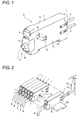
- the photoelectric sensor units 1 each include a housing 2 having a flat, substantially rectangular solid shape.
- An out-bound optical fiber cable 4 and an in-bound optical fiber cable 5 are drawn out from a rear end portion 3 of the housing 2.
- Leading ends of the optical fiber cables 4 and 5 are connected to sensor heads 4a and 5a disposed in a detection area.
- An electric cable (electric cord) 8 is drawn out from a front end portion 6 of the housing 2 with a connector 7 interposed therebetween.
- the electric cable 8 is used to lead an output signal (for example, on and off signals or a light quantity value signal) of a sensing system circuit (not illustrated) in the housing 2.
- the electric cable 8 is connected to a control device (not illustrated) such as a Programmable Logic Controller (PLC).
- PLC Programmable Logic Controller
- a DIN rail mounting groove 9 used to mount the housing 2 is formed in a bottom surface of the housing 2.
- An optical communication window 12 for right-hand communication is disposed in a right side surface 11 of the housing 2, and an optical communication window 14 for left-hand communication is disposed in a left side surface 13 of the housing 2.
- the optical communication windows 12 and 14 are illustrated as a through-hole in Fig. 1 . However, actually the optical communication windows 12 and 14 are closed by resin filters, and formed into flat surfaces flush with the side surfaces of the housing 2. The resin filter transmits an infrared ray and cuts off a visible ray.
- a pair of a light emitting element and a light receiving element (not illustrate) for right-hand communication is disposed behind the optical communication window 12 of the right side surface, and the infrared ray is used in the pair of the light emitting element and the light receiving element for right-hand communication.
- a pair of a light emitting element and a light receiving element (not illustrate) for left-hand communication is disposed behind the optical communication window 14 of the left side surface, and the infrared ray is used in the pair of the light emitting element and the light receiving element for left-hand communication.
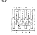
- Fig. 2 illustrates the state in which many photoelectric sensor units 1 are mounted on a DIN rail.
- the many photoelectric sensor units 1 are closely mounted on a DIN rail 10 using the DIN rail mounting groove 9 provided in the bottom surface of each photoelectric sensor unit 1, the photoelectric sensor units 1 are closely adjacent to each other and arranged in line.
- the optical communication window 12 and the optical communication window 14 are opposed to each other. Therefore, as indicated by an arrow 15 in Fig. 2 , bidirectional optical communication in which the infrared ray is used can be conducted between the photoelectric sensor units 1 and 1 adjacent to each other through the optical communication windows 12 and 14.
- Fig. 3 is a sectional view of the housing 2, and illustrates an example of a support structure of the light emitting element and the light receiving element in the housing 2 of the photoelectric sensor unit 1.
- Fig. 3 illustrates the state in which three photoelectric sensor units 1 a, 1 b, and 1 c are disposed while being closely adjacent to each other.
- a circuit board 16 on which various circuit components are mounted is accommodated in the housing 2 of each of the photoelectric sensor units 1 a, 1 b, and 1 c.
- the circuit board 16 is supported by a support mechanism (not illustrated) in an attitude parallel to the right and left side surfaces 11 and 13 of the housing 2.
- a right-hand communication light emitting element (for example, an infrared-emitting diode) 17 and a light receiving element (for example, photodiode) 18 are attached to a right side surface of the circuit board 16 in Fig. 3 .
- the elements 17 and 18 are positioned so as to be opposed to the optical communication window 12 provided in the right side surface 11 of the housing 2.
- a left-hand communication light receiving element (for example, a photodiode) 19 and a light emitting element (for example, an infrared-emitting diode) 20 are attached to a left side surface of the circuit board 16 in Fig. 3 .
- the elements 19 and 20 are positioned so as to be opposed to the optical communication window 14 provided in the left side surface 13 of the housing 2.
- the right and left optical communication windows 12 and 14 are closed by a visible ray cutoff filter.
- a signal can be transmitted toward a direction indicated by an arrow A in Fig. 3 by repeatedly performing processing, in which the light emitted from the light emitting element 17 is received by the light receiving element 19, between the sensor units adjacent to each other.
- a signal can be transmitted toward a direction indicated by an arrow B in Fig. 3 by repeatedly performing processing, in which the light emitted from the light emitting element 20 is received by the light receiving element 18, between the sensor units adjacent to each other. That is, in the example in Fig. 3 , data can bi-directionally be transmitted among the photoelectric sensor units 1 a, 1 b, and 1 c.
- a lens that improves light transmission/reception efficiency between the light emitting element and the light receiving element, which are opposed to each other between the sensor units adjacent to each other, may be disposed in the right and left optical communication windows 12 and 14 of the housing 2.
- any suitable optical lens or Fresnel lens can be used as the lens.
- the photoelectric sensor unit 1 is constructed by various processing functions implemented as software by a CPU (Central Processing Unit) 100 and various processing functions implemented as hardware by a dedicated circuit.
- CPU Central Processing Unit
- the CPU 100 controls a light projection controller 203 to cause a light emitting element (LED) 201 to emit the infrared ray. More specifically, the CPU 100 controls the light projection controller 203 such that the light emitting element 201 operates (more specifically, projects the light) after a delay time T that is determined individually for each photoelectric sensor unit 1 elapses with a synchronization signal as a starting point.
- the synchronization signal is transmitted from the photoelectric sensor unit 1 recognized as the master unit in the plurality of photoelectric sensor units 1.
- the delay time T of each photoelectric sensor unit 1 is determined such that a light projecting period (which may also be referred to as "operating period") matches with a predetermined period TF, and that the delay time T differs from the delay time T of any other sensor unit of the same sensor type.
- the predetermined period TF is determined (set) individually for each sensor type. In other words, no two sensor units of the same sensor type have the same delay time T. However two or more sensor units of different sensor types may have the same delay time T.
- the sensor types of the photoelectric sensor units 1 are represented by their respective type information. Each photoelectric sensor unit 1 retains such type information.
- a signal that is generated by the light reception of a light receiving element (PD) 202 is amplified by an amplifier circuit 204, converted into a digital signal by an A/D converter 205, and taken in the CPU 100.
- the CPU 100 directly binarizes the light reception data, or binarizes the light reception data by a comparison to a previously-set threshold. Then the CPU 100 transmits the binarized data to the outside.
- the CPU 100 controls left light projecting circuit 211 and right light projecting circuit 213 to cause left communication light emitting element (LED) 207 and right communication light emitting element (LED) 209 to emit the infrared rays to the adjacent photoelectric sensor units.
- the infrared rays coming from the adjacent right and left photoelectric sensor units are received by left light receiving element (PD) 206 and right light receiving element (PD) 208, and the light reception signals are transmitted to the CPU 100 through light receiving circuits 210 and 212.
- the CPU 100 conducts optical communication with the right and left adjacent sensors by controlling the transmitted and received signals based on a predetermined protocol.
- the light receiving element 206, the communication light emitting element 209, the light receiving circuit 210, and the light projecting circuit 213 are used to transmit and receive the synchronization signal that prevents mutual interference between the photoelectric sensor units 1. Specifically, in each photoelectric sensor unit 1, the light receiving circuit 210 and the light projecting circuit 213 are directly connected to each other. This configuration quickly transmits the received synchronization signal from the communication light emitting element 209 to adjacent another photoelectric sensor unit 1 through the light projecting circuit 213 while the CPU 100 does not perform delay processing.
- the one photoelectric sensor unit 1 recognized as the master unit from the plurality of photoelectric sensor units 1 transmits the synchronization signal with a predetermined period.
- the photoelectric sensor unit 1 in which the light receiving element 206 does not receive the infrared ray in a period during which all the photoelectric sensor units 1 are controlled such that the communication light emitting element 209 emits the infrared ray, recognizes itself as the master unit. That is, in the photoelectric sensor units 1 arranged in line, one of the photoelectric sensor units 1 located at both ends is the master unit.
- the CPU 100 controls lighting of a display unit 214.
- the CPU 100 processes a signal from a setting switch 215.
- a signal generated by the CPU 100 is transmitted to the PLC through an output circuit 216.
- a signal obtained from a reset unit 217 is transmitted to the CPU 100 to reset measurement control.
- a power supply circuit 218 supplies a power necessary to drive the CPU 100.
- Various kinds of data necessary for the operation of the CPU 100 are stored in a recording medium such as an EEPROM (Electrically Erasable Programmable Read Only Memory) 219.
- a reference clock is input from an oscillator (OSC) 220 to the CPU 100.
- OSC oscillator
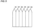
- Figs. 5 and 6 illustrate an example in which three photoelectric sensor units 100a, 100b, and 100c of a type A and three photoelectric sensor units 200a, 200b, and 200c of a type B are used.
- the number of types of the photoelectric sensor unit and the number of photoelectric sensor units of each type are not limited to those in Figs. 5 and 6 .
- the photoelectric sensor unit 100a is the master unit. It is also assumed that the photoelectric sensor unit 100b, the photoelectric sensor unit 200a, the photoelectric sensor unit 100c, the photoelectric sensor unit 200b, and the photoelectric sensor unit 200c, which are slave units, are disposed in that order next to the master unit.
- the channel (CH) number of the photoelectric sensor unit 100a is recognized as "1".
- the channel number of photoelectric sensor unit 100b is recognized as “2”.
- the channel number of the photoelectric sensor unit 200a is recognized as "3".
- the channel number of the photoelectric sensor unit 100c is recognized as "4".
- the channel number of the photoelectric sensor unit 200b is recognized as "5".
- the channel number of the photoelectric sensor unit 200c is recognized as "6".
- the photoelectric sensor unit 100a recognized as the master unit transmits the synchronization signal with a predetermined period T0.
- Each photoelectric sensor unit projects the light after the delay time T determined for that photoelectric sensor unit elapses with the transmitted synchronization signal as the starting point (for example, after the synchronization signal has been received or recognized by that photoelectric sensor unit).
- the delay time T of each photoelectric sensor unit is determined so as to differ from the delay time T of the other photoelectric sensor units of the identical sensor type (i.e. the other photoelectric sensor units having the identical type information).
- a delay time T1(1) of the master unit (the photoelectric sensor unit 100a) with respect to the synchronization signal transmitted for a first time is DA0 (DA0 ⁇ 0).
- the delay time DA0 is previously determined by the developer.
- a delay time T2(1) of the photoelectric sensor unit 100b with respect to the synchronization signal transmitted for the first time is DA0 + DA1 (DA1 > 0).
- the time DA1 may be previously determined by the developer based on a detection principle of the sensor and a light projecting period TFA determined from specifications of the type A. For example, the time DA1 may be determined such that the light projecting period TFA of the type A is longer than the sum of the delay times of the photoelectric sensor units of the type A.
- a delay time T4(1) of the photoelectric sensor unit 100c with respect to the synchronization signal transmitted for the first time is DA0 + 2 ⁇ DA1.
- a delay time T3(1) of the photoelectric sensor unit 200a with respect to the synchronization signal transmitted for the first time is DB0 (DB0 ⁇ 0).
- the delay time DB0 may be previously determined by the developer.
- a delay time T5(1) of the photoelectric sensor unit 200b with respect to the synchronization signal transmitted for the first time is DB0 + DB1 (DB1 > 0).
- the time DB1 may be previously determined by the developer based on the detection principle of the sensor and a light projecting period TFB of the type B. For example, the time DB1 may be determined such that the light projecting period TFB determined from specifications of the type B is longer than the sum of the delay times of the photoelectric sensor units of the type B.
- a delay time T6(1) of the photoelectric sensor unit 200c with respect to the synchronization signal transmitted for the first time is DA0 + 2 ⁇ DB1.
- the delay timer are determined such that they increase successively by a predetermined time length in the light projection order for each type. That is, the delay times of the photoelectric sensor units of the type A are determined such that they increase successively by the time DA1. The delay times of the photoelectric sensor units of the type B are determined such that they increase successively by the time DB1.
- Each of the delay times T1(2), T2(2), T3(2), T4(2), T5(2), and T6(2) of the photoelectric sensor units with respect to the synchronization signal transmitted for the second time is determined such that the light projecting period of each photoelectric sensor unit matches (coincides) with a predetermined period that is determined individually for each sensor type (as represented by the type information), and such that the light projecting period differs from the delay time of the other photoelectric sensor units having the same sensor type (i.e. the identical type information).
- the delay times T1(2), T2(2), and T4(2) of the photoelectric sensor units of the type A are determined such that the actual light projecting period of each photoelectric sensor unit matches with the predetermined light projecting period TFA, which has been determined for type A sensor units, and such that the each of those delay times differs from the delay time of any other photoelectric sensor of the identical type.
- the delay times T3(2), T5(2), and T6(2) of the photoelectric sensor units of the type B are determined such that the actual light projecting period of each photoelectric sensor unit matches with the predetermined light projecting period TFB, which has been determined for type B sensor units, and such that each of those delay times differs from the delay time of any other photoelectric sensor of the identical type.
- the delay time of each photoelectric sensor unit with respect to the synchronization signal transmitted for a third time or subsequent times is determined such that the actual light projecting period of each photoelectric sensor unit matches with the predetermined period TF determined for the respective sensor type, and such that the delay time of the respective photoelectric sensor unit differs from the delay time of any other photoelectric sensor of the same type (i.e. with the identical type information).
- each photoelectric sensor unit 1 recognizes its channel number. Processing in which each photoelectric sensor unit 1 recognizes its channel number will be described below with reference to Fig. 7 .
- Step (hereinafter, Step is abbreviated to S) 100 each photoelectric sensor unit 1 sets both an infrared input port and an infrared output port to a general-purpose input/output allocation, and turns on an infrared output for a predetermined time interval. That is, the communication light emitting element 209 emits the infrared ray for the predetermined time interval.
- the channel number is recognized as "1" in S104. That is, the photoelectric sensor unit 1 is recognizes itself as the master unit.
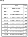
- each photoelectric sensor unit 1 switches both the infrared input port and the infrared output port to a UART (Universal Asynchronous Receiver Transmitter) allocation, and the photoelectric sensor unit 1 that is the master unit transmits the binary data shown in Fig. 8 to the adjacent photoelectric sensor unit 1 (for example, a neighbor on the right) using the infrared output.
- the binary data is repeatedly output at least a predetermined number of times in consideration of different power-on timing. That the channel number of the master unit is a channel 1 is expressed by inputting data "0x01" as its "own CH number".
- That one photoelectric sensor unit 1 of the type A is recognized is expressed by inputting data "0x01” as "the number of sensors of type A". That is, the master unit that transmits the binary data in Fig. 8 has the type "A". For example, in the case that the master unit has the type "B", data "0x00” is input as “the number of sensors of type A” while data "0x01” is input as "the number of sensors of type B". The type information indicating the type of the photoelectric sensor unit 1 is retained by each photoelectric sensor unit 1.
- the number of sensors in each type also expresses an order m of the sensor in each type.
- the order m is "1" in a group of the photoelectric sensor units 1 of the type A is expressed by inputting data "0x01" as "the number of sensors of type A".
- the infrared input port and the infrared output port are set to general-purpose input/output allocation
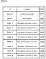
- the photoelectric sensor unit 1 that receives the binary data namely, the photoelectric sensor unit 1 that is one of the slave units transmits the binary data in Fig. 9 to the adjacent photoelectric sensor unit 1 (for example, the neighbor on the right) using the infrared output. Because data "0x01" is input to the "own CH number" of the received binary data, the photoelectric sensor unit 1 that receives the binary data recognizes itself as a channel 2. That is, the number that is larger than the channel number expressed by the "own CH number" of the received binary data by 1 is recognized as the channel number. In the binary data in Fig.
- data "0x02" is input as the "own CH number” in order to increment the channel number by 1 to express that the channel number is the channel 2. Therefore, in the case that data "0x05” is input to the "own CH number” of the received binary data, data "0x06” is input to the "own CH number" of the transmitted binary data.
- each photoelectric sensor unit 1 recognizes the number, which is larger than the channel number expressed by the "own CH number" of the received binary data by 1, as the channel number.
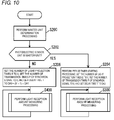
- FIG. 10 illustrates the processing that is performed by the photoelectric sensor unit 1 of the type "A” in order to set the delay time T by way of example.
- the processing that is performed by the photoelectric sensor unit 1 of the type "B” in order to set the delay time T differs from the processing that is performed by the photoelectric sensor unit 1 of the type "A” in order to set the delay time T only in that the "time DB0" and the "time DB1" are used instead of the "time DA0" and the "time DA1". The same holds true for the case that the type different from the type A and the time B is used.
- each photoelectric sensor unit 1 determines whether it is the master unit or a slave unit in S200.
- the photoelectric sensor unit 1 is the master unit (YES in S202)
- S204 processing of starting a period timer is performed, the number of light projection times E in order to detect a workpiece is set (reset) to "0", the number of transmission times P of the synchronization signal is set (reset) to "0", and the delay time T is set to the time DA0.
- the delay time T set in S204 is an initial value of the delay time T of the master unit. Then processing of measuring the light reception amount is performed in order to detect the workpiece in S300.
- the photoelectric sensor unit 1 is a slave unit (NO in S202), in S206, the number of light projection times E is set (reset) to "0" in order to detect the workpiece, the number of reception times of the synchronization signal, namely the number of transmission times P of the synchronization signal is set (reset) to "0", and the delay time T is set to time DA0 + (m - 1) ⁇ DA1.
- "m” is the ordinal number of the sensor among sensors of the same type, which is expressed by "the number of sensors of type A" of the binary data, for example.
- the delay time T set in S206 is the initial value of the delay time T of the slave unit. Then processing of measuring the light reception amount is performed in order to detect the workpiece in S400.
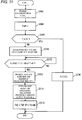
- Fig. 11 illustrates an example when the master unit is a photoelectric sensor unit 1 of the type "A".
- the case that the master unit is a photoelectric sensor unit 1 of the type "B” differs from the case that the master unit is a photoelectric sensor unit 1 of the type "A” only in that the "time DB0" is used instead of the "time DA0" and that the "light projecting period TFB" is used instead of the "light projecting period TFA".
- the type different from the type A and the time B is used.
- the master unit transmits the synchronization signal in S302, the number of transmission times P of the synchronization signal is incremented by 1 in S304.
- the delay time T is reset so as to be shorter than the period T0 in S306. Specifically, the delay time T is shortened by the transmission period T0 of the synchronization signal.
- the elapsed time since the synchronization signal is transmitted is set (reset) to "0", and the count of the elapsed time is started.
- the elapsed time exceeds the delay time T (YES in S310)
- the light is projected from the sensor head 4a, and the number of light projection times E is incremented by "1 ".
- the delay times T from the initial value are set in S316.
- the delay time T is determined such that the light projecting period matches with the predetermined period TFA, which has been determined for type A sensor units, and such that the light projecting period differs from the delay time T of any other photoelectric sensor unit of the identical type. More specifically, the delay time T is calculated based on the following equation.
- delay time T E ⁇ TFA - P ⁇ T ⁇ 0 + DA ⁇ 0 Processing performed by the slave unit in order to measure the light reception amount will be described with reference to Fig. 12.
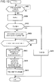
- Fig. 12 illustrates an example when the slave unit is the photoelectric sensor unit 1 of the type "A".
- the case that the slave unit is a photoelectric sensor unit 1 of the type "B" differs from the case that the slave unit is a photoelectric sensor unit 1 of the type "A” only in that the "time DB0" and the “time DB1” are used instead of the "time DA0" and the “time DA1” and that the "light projecting period TFB" is used instead of the "light projecting period TFA".
- the type different from the type A and the time B is used.
- the slave unit When the slave unit receives the synchronization signal (YES in S402), the number of transmission times P of the synchronization signal is incremented by "1" in S404.
- the delay time T is reset so as to be shorter than the period T0 in S406. Specifically, the delay time T is shortened by the transmission period T0 of the synchronization signal.
- the elapsed time since the synchronization signal is transmitted is set (reset) to "0", and the count of the elapsed time is started.
- the elapsed time exceeds the delay time T (YES in S410)
- the light is projected from the sensor head 4a, and the number of light projection times E is incremented by "1 ".
- the delay times T from the initial value are set in S416.
- the delay time T is determined such that the light projecting period matches with the predetermined period TFA determined in each type, and such that the light projecting period differs from the delay time T of another photoelectric sensor unit of the identical type. More specifically, the delay time T is calculated based on the following equation.
- delay time T E ⁇ TFA - P ⁇ T ⁇ 0 + DA ⁇ 0 + m - 1 ⁇ DA ⁇ 1
- the disclosed embodiment is described only by way of example, but not restrictive in all points. The scope of the present invention is indicated by not the above description but the claims, and the meanings equivalent to the claims and all the changes within the claims are also included in the present invention.
Landscapes
- Engineering & Computer Science (AREA)
- Physics & Mathematics (AREA)
- Computer Networks & Wireless Communication (AREA)
- Remote Sensing (AREA)
- Radar, Positioning & Navigation (AREA)
- General Physics & Mathematics (AREA)
- Electromagnetism (AREA)
- Signal Processing (AREA)
- Spectroscopy & Molecular Physics (AREA)
- Geophysics And Detection Of Objects (AREA)
- Electronic Switches (AREA)
- Switches Operated By Changes In Physical Conditions (AREA)
- Photometry And Measurement Of Optical Pulse Characteristics (AREA)
Abstract
Description
- The present invention relates to a sensor system, particularly to a technology for controlling a light projecting time of each sensor unit in a sensor system including a plurality of sensor units.
- In a production line, whether a workpiece (a detection target object) is present is determined based on a physical amount such as a light reception amount detected by a sensor. The physical amount is detected at a plurality of points. That is, the plurality of sensors are provided. At this point, for example, a light receiving unit of a photoelectric sensor is occasionally disposed near a light receiving unit of another photoelectric sensor. In this case, light projected from a certain photoelectric sensor may be incident on a light receiving unit of another photoelectric sensor, degrading determination accuracy. Therefore, there is provided a technique of preventing mutual interference by varying an operation time of the sensor.
- Japanese Patent No.
3478646 3478646 - However, in Japanese Patent No.
3478646 - The present invention has been devised to solve the problems described above, and an object thereof is to provide the light projecting period arbitrarily determined in each type and prevent the mutual interference between identical types in a sensor system including a plurality of sensor units.
- In accordance with one aspect of the present invention, a sensor system includes a plurality of sensor units that are coupled in such a manner that signal transmission among the sensor units is possible. Each of the sensor units retains type information indicating a sensor type of the respective sensor unit, and sets a unique identification number of the respective sensor unit by signal transmission among the sensor units. Each of the sensor units operates after a delay time determined according to the identification number of the respective sensor unit elapses with a synchronization signal as a starting point. The synchronization signal is transmitted with a predetermined period from one of the plurality of sensor units that has a specific identification number. The delay time of each of the sensor units is determined such that an operating period of the respective sensor unit matches with a predetermined period, which is determined individually for each sensor type, and such that the delay time differs from the delay time of any other sensor unit having the same sensor type. That the sensor units are of different sensor types may mean that, for example, the sensor units differ from each other in an operating (light projection) time or a wavelength, a period, an amplitude, and/or a frequency of the projected light. The delay time may be determined so that it is successively increased by a predetermined time, in operation order and individually for each sensor type. Examples of the "sensor units" include photoelectric sensor units, ultrasonic sensor units, and proximity sensor units.
- Because the sensor units of identical types differ from each other in their operation time, the mutual interference is prevented between identical types. Because the operation time has no influence between the different types, the operating period can arbitrarily be set for each of the plurality of types. Although there may be an overlap in the operation times of different sensor types, the light can be distinguished from a characteristic other than the light reception time if the types differ from each other. Therefore, there is little influence on the determination accuracy.
- The delay time may be shortened if the delay time is longer than a transmission period of the synchronization signal, the sensor system may not operated in the transmission period, and the shortened delay may be determined as a delay time of the next transmission period. In this case, the delay time may be shortened by the transmission period. An operating period of each type may be longer than the sum of the delay times of the sensor units of the same type (i.e. having the identical type information).
- The sensor units may be disposed adjacent to each other. In this case, the sensor units adjacent to each other may be coupled by a connector means in such a manner that signal transmission among the sensor units is possible.
- The connector means (which may also be referred to as "connector unit") may be an optical connector that comprises a pair of a light projecting element and a light receiving element. In this case, a driving circuit of the light receiving element may electrically be connected to a driving circuit of the light projecting element in the sensor unit. A difference between a light reception time in the light receiving element and a light projecting time from the light projecting element can be decreased by electrically connecting the driving circuit of the light receiving element to the driving circuit of the light projecting element in the sensor unit. Therefore, a signal transmission delay can be decreased.
-
-
Fig. 1 is a perspective view illustrating a photoelectric sensor unit; -
Fig. 2 is a perspective view illustrating a state in which the photoelectric sensor units are arrayed; -
Fig. 3 is a sectional view illustrating a positional relationship between a disposition of light projecting/light receiving element and an optical communication window in the photoelectric sensor unit; -
Fig. 4 is a view illustrating an internal configuration of the photoelectric sensor unit; -
Fig. 5 is a view illustrating a sensor system in which three photoelectric sensor units of a type A and three photoelectric sensor units of a type B are arrayed; -
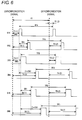
Fig. 6 is a view illustrating a delay time of each photoelectric sensor unit; -
Fig. 7 is a flowchart illustrating processing, which is performed by each photoelectric sensor unit in order to recognize a channel number; -
Fig. 8 is a view illustrating binary data transmitted by a master unit; -
Fig. 9 is a view illustrating binary data transmitted by a slave unit; -
Fig. 10 is a flowchart illustrating processing, which is performed by the photoelectric sensor unit in order to set a delay time; -
Fig. 11 is a flowchart illustrating processing, which is performed by the master unit in order to measure a light reception amount; and -
Fig. 12 is a flowchart illustrating processing, which is performed by the slave unit in order to measure the light reception amount. - Hereinafter, an embodiment of the present invention will be described with reference to the drawings. In the drawings, identical components are designated by identical numerals, and their names and functions are also identical. Accordingly, their description is not repeated.
- Referring to
Fig. 2 , a sensor system of the embodiment includes a plurality of sensor types ofphotoelectric sensor units 1. For example, the types are distinguished from each other by operating (light projecting) time and wavelength, period, amplitude, and/or frequency of the projected light. That is, the various sensor types differ from each other in the light projecting time, the wavelength, the period, the amplitude, and/or the frequency of the projected light. For example, ultrasonic sensor units and/or proximity sensor units may be included in the sensor system instead of or in addition to thephotoelectric sensor units 1. - Referring to
Fig. 1 , by way of example, eachphotoelectric sensor unit 1 is a fiber typephotoelectric sensor unit 1. Thephotoelectric sensor units 1 each include ahousing 2 having a flat, substantially rectangular solid shape.
An out-boundoptical fiber cable 4 and an in-boundoptical fiber cable 5 are drawn out from arear end portion 3 of thehousing 2. Leading ends of theoptical fiber cables sensor heads 4a and 5a disposed in a detection area. - An electric cable (electric cord) 8 is drawn out from a
front end portion 6 of thehousing 2 with aconnector 7 interposed therebetween. Theelectric cable 8 is used to lead an output signal (for example, on and off signals or a light quantity value signal) of a sensing system circuit (not illustrated) in thehousing 2. For example, theelectric cable 8 is connected to a control device (not illustrated) such as a Programmable Logic Controller (PLC). A DINrail mounting groove 9 used to mount thehousing 2 is formed in a bottom surface of thehousing 2. - An
optical communication window 12 for right-hand communication is disposed in aright side surface 11 of thehousing 2, and anoptical communication window 14 for left-hand communication is disposed in aleft side surface 13 of thehousing 2. Theoptical communication windows Fig. 1 . However, actually theoptical communication windows housing 2. The resin filter transmits an infrared ray and cuts off a visible ray. - A pair of a light emitting element and a light receiving element (not illustrate) for right-hand communication is disposed behind the
optical communication window 12 of the right side surface, and the infrared ray is used in the pair of the light emitting element and the light receiving element for right-hand communication. A pair of a light emitting element and a light receiving element (not illustrate) for left-hand communication is disposed behind theoptical communication window 14 of the left side surface, and the infrared ray is used in the pair of the light emitting element and the light receiving element for left-hand communication. -
Fig. 2 illustrates the state in which manyphotoelectric sensor units 1 are mounted on a DIN rail. As illustrated inFig. 2 , when the manyphotoelectric sensor units 1 are closely mounted on aDIN rail 10 using the DINrail mounting groove 9 provided in the bottom surface of eachphotoelectric sensor unit 1, thephotoelectric sensor units 1 are closely adjacent to each other and arranged in line. At this point, theoptical communication window 12 and theoptical communication window 14 are opposed to each other. Therefore, as indicated by anarrow 15 inFig. 2 , bidirectional optical communication in which the infrared ray is used can be conducted between thephotoelectric sensor units optical communication windows -
Fig. 3 is a sectional view of thehousing 2, and illustrates an example of a support structure of the light emitting element and the light receiving element in thehousing 2 of thephotoelectric sensor unit 1.Fig. 3 illustrates the state in which threephotoelectric sensor units 1 a, 1 b, and 1 c are disposed while being closely adjacent to each other. - As illustrated in
Fig. 3 , acircuit board 16 on which various circuit components are mounted is accommodated in thehousing 2 of each of thephotoelectric sensor units 1 a, 1 b, and 1 c. Thecircuit board 16 is supported by a support mechanism (not illustrated) in an attitude parallel to the right and left side surfaces 11 and 13 of thehousing 2. - A right-hand communication light emitting element (for example, an infrared-emitting diode) 17 and a light receiving element (for example, photodiode) 18 are attached to a right side surface of the
circuit board 16 inFig. 3 . The elements 17 and 18 are positioned so as to be opposed to theoptical communication window 12 provided in theright side surface 11 of thehousing 2. Similarly, a left-hand communication light receiving element (for example, a photodiode) 19 and a light emitting element (for example, an infrared-emitting diode) 20 are attached to a left side surface of thecircuit board 16 inFig. 3 . The elements 19 and 20 are positioned so as to be opposed to theoptical communication window 14 provided in theleft side surface 13 of thehousing 2. Although not illustrated inFig. 3 , the right and leftoptical communication windows - According to the above configuration, a signal can be transmitted toward a direction indicated by an arrow A in
Fig. 3 by repeatedly performing processing, in which the light emitted from the light emitting element 17 is received by the light receiving element 19, between the sensor units adjacent to each other. A signal can be transmitted toward a direction indicated by an arrow B inFig. 3 by repeatedly performing processing, in which the light emitted from the light emitting element 20 is received by the light receiving element 18, between the sensor units adjacent to each other. That is, in the example inFig. 3 , data can bi-directionally be transmitted among thephotoelectric sensor units 1 a, 1 b, and 1 c. - A lens that improves light transmission/reception efficiency between the light emitting element and the light receiving element, which are opposed to each other between the sensor units adjacent to each other, may be disposed in the right and left
optical communication windows housing 2. For example, any suitable optical lens or Fresnel lens can be used as the lens. - An internal structure of the
photoelectric sensor unit 1 will be described with reference toFig. 4 . Thephotoelectric sensor unit 1 is constructed by various processing functions implemented as software by a CPU (Central Processing Unit) 100 and various processing functions implemented as hardware by a dedicated circuit. - The
CPU 100 controls alight projection controller 203 to cause a light emitting element (LED) 201 to emit the infrared ray. More specifically, theCPU 100 controls thelight projection controller 203 such that thelight emitting element 201 operates (more specifically, projects the light) after a delay time T that is determined individually for eachphotoelectric sensor unit 1 elapses with a synchronization signal as a starting point. The synchronization signal is transmitted from thephotoelectric sensor unit 1 recognized as the master unit in the plurality ofphotoelectric sensor units 1. The delay time T of eachphotoelectric sensor unit 1 is determined such that a light projecting period (which may also be referred to as "operating period") matches with a predetermined period TF, and that the delay time T differs from the delay time T of any other sensor unit of the same sensor type. It should be noted that the predetermined period TF is determined (set) individually for each sensor type. In other words, no two sensor units of the same sensor type have the same delay time T. However two or more sensor units of different sensor types may have the same delay time T. The sensor types of thephotoelectric sensor units 1 are represented by their respective type information. Eachphotoelectric sensor unit 1 retains such type information. - A signal that is generated by the light reception of a light receiving element (PD) 202 is amplified by an
amplifier circuit 204, converted into a digital signal by an A/D converter 205, and taken in theCPU 100. TheCPU 100 directly binarizes the light reception data, or binarizes the light reception data by a comparison to a previously-set threshold. Then theCPU 100 transmits the binarized data to the outside. - The
CPU 100 controls leftlight projecting circuit 211 and rightlight projecting circuit 213 to cause left communication light emitting element (LED) 207 and right communication light emitting element (LED) 209 to emit the infrared rays to the adjacent photoelectric sensor units. The infrared rays coming from the adjacent right and left photoelectric sensor units are received by left light receiving element (PD) 206 and right light receiving element (PD) 208, and the light reception signals are transmitted to theCPU 100 through light receivingcircuits CPU 100 conducts optical communication with the right and left adjacent sensors by controlling the transmitted and received signals based on a predetermined protocol. - The
light receiving element 206, the communicationlight emitting element 209, thelight receiving circuit 210, and thelight projecting circuit 213 are used to transmit and receive the synchronization signal that prevents mutual interference between thephotoelectric sensor units 1. Specifically, in eachphotoelectric sensor unit 1, thelight receiving circuit 210 and thelight projecting circuit 213 are directly connected to each other. This configuration quickly transmits the received synchronization signal from the communicationlight emitting element 209 to adjacent anotherphotoelectric sensor unit 1 through thelight projecting circuit 213 while theCPU 100 does not perform delay processing. - As described above, the one
photoelectric sensor unit 1 recognized as the master unit from the plurality ofphotoelectric sensor units 1 transmits the synchronization signal with a predetermined period. For example, thephotoelectric sensor unit 1, in which thelight receiving element 206 does not receive the infrared ray in a period during which all thephotoelectric sensor units 1 are controlled such that the communicationlight emitting element 209 emits the infrared ray, recognizes itself as the master unit. That is, in thephotoelectric sensor units 1 arranged in line, one of thephotoelectric sensor units 1 located at both ends is the master unit. - The
CPU 100 controls lighting of adisplay unit 214. TheCPU 100 processes a signal from a settingswitch 215. A signal generated by theCPU 100 is transmitted to the PLC through anoutput circuit 216. A signal obtained from areset unit 217 is transmitted to theCPU 100 to reset measurement control. Apower supply circuit 218 supplies a power necessary to drive theCPU 100. Various kinds of data necessary for the operation of theCPU 100 are stored in a recording medium such as an EEPROM (Electrically Erasable Programmable Read Only Memory) 219. A reference clock is input from an oscillator (OSC) 220 to theCPU 100. - A mutual interference preventing operation in the sensor system in which the plurality of
photoelectric sensor units 1 are used will be described below with reference toFigs. 5 and6 . -
Figs. 5 and6 illustrate an example in which threephotoelectric sensor units photoelectric sensor units Figs. 5 and6 . - In
Figs. 5 and6 , it is assumed that thephotoelectric sensor unit 100a is the master unit. It is also assumed that thephotoelectric sensor unit 100b, thephotoelectric sensor unit 200a, thephotoelectric sensor unit 100c, thephotoelectric sensor unit 200b, and thephotoelectric sensor unit 200c, which are slave units, are disposed in that order next to the master unit. - In the example in
Figs. 5 and6 , the channel (CH) number of thephotoelectric sensor unit 100a is recognized as "1". Similarly, the channel number ofphotoelectric sensor unit 100b is recognized as "2". The channel number of thephotoelectric sensor unit 200a is recognized as "3". The channel number of thephotoelectric sensor unit 100c is recognized as "4". The channel number of thephotoelectric sensor unit 200b is recognized as "5". The channel number of thephotoelectric sensor unit 200c is recognized as "6". - As described above, in the embodiment, the
photoelectric sensor unit 100a recognized as the master unit transmits the synchronization signal with a predetermined period T0. Each photoelectric sensor unit projects the light after the delay time T determined for that photoelectric sensor unit elapses with the transmitted synchronization signal as the starting point (for example, after the synchronization signal has been received or recognized by that photoelectric sensor unit). The delay time T of each photoelectric sensor unit is determined so as to differ from the delay time T of the other photoelectric sensor units of the identical sensor type (i.e. the other photoelectric sensor units having the identical type information). - Specifically, a delay time T1(1) of the master unit (the
photoelectric sensor unit 100a) with respect to the synchronization signal transmitted for a first time is DA0 (DA0 ≥ 0). The delay time DA0 is previously determined by the developer. - A delay time T2(1) of the
photoelectric sensor unit 100b with respect to the synchronization signal transmitted for the first time is DA0 + DA1 (DA1 > 0). The time DA1 may be previously determined by the developer based on a detection principle of the sensor and a light projecting period TFA determined from specifications of the type A. For example, the time DA1 may be determined such that the light projecting period TFA of the type A is longer than the sum of the delay times of the photoelectric sensor units of the type A. - A delay time T4(1) of the
photoelectric sensor unit 100c with respect to the synchronization signal transmitted for the first time is DA0 + 2 × DA1. - A delay time T3(1) of the
photoelectric sensor unit 200a with respect to the synchronization signal transmitted for the first time is DB0 (DB0 ≥ 0). The delay time DB0 may be previously determined by the developer. - A delay time T5(1) of the
photoelectric sensor unit 200b with respect to the synchronization signal transmitted for the first time is DB0 + DB1 (DB1 > 0). The time DB1 may be previously determined by the developer based on the detection principle of the sensor and a light projecting period TFB of the type B. For example, the time DB1 may be determined such that the light projecting period TFB determined from specifications of the type B is longer than the sum of the delay times of the photoelectric sensor units of the type B. - A delay time T6(1) of the
photoelectric sensor unit 200c with respect to the synchronization signal transmitted for the first time is DA0 + 2 × DB1. - As is clear from the above description, in this embodiment, the delay timer are determined such that they increase successively by a predetermined time length in the light projection order for each type. That is, the delay times of the photoelectric sensor units of the type A are determined such that they increase successively by the time DA1. The delay times of the photoelectric sensor units of the type B are determined such that they increase successively by the time DB1.
- Each of the delay times T1(2), T2(2), T3(2), T4(2), T5(2), and T6(2) of the photoelectric sensor units with respect to the synchronization signal transmitted for the second time is determined such that the light projecting period of each photoelectric sensor unit matches (coincides) with a predetermined period that is determined individually for each sensor type (as represented by the type information), and such that the light projecting period differs from the delay time of the other photoelectric sensor units having the same sensor type (i.e. the identical type information).
- That is, the delay times T1(2), T2(2), and T4(2) of the photoelectric sensor units of the type A are determined such that the actual light projecting period of each photoelectric sensor unit matches with the predetermined light projecting period TFA, which has been determined for type A sensor units, and such that the each of those delay times differs from the delay time of any other photoelectric sensor of the identical type.
- Similarly, the delay times T3(2), T5(2), and T6(2) of the photoelectric sensor units of the type B are determined such that the actual light projecting period of each photoelectric sensor unit matches with the predetermined light projecting period TFB, which has been determined for type B sensor units, and such that each of those delay times differs from the delay time of any other photoelectric sensor of the identical type.
- The delay time of each photoelectric sensor unit with respect to the synchronization signal transmitted for a third time or subsequent times is determined such that the actual light projecting period of each photoelectric sensor unit matches with the predetermined period TF determined for the respective sensor type, and such that the delay time of the respective photoelectric sensor unit differs from the delay time of any other photoelectric sensor of the same type (i.e. with the identical type information).
- Processing in which each
photoelectric sensor unit 1 recognizes its channel number will be described below with reference toFig. 7 . - In Step (hereinafter, Step is abbreviated to S) 100, each
photoelectric sensor unit 1 sets both an infrared input port and an infrared output port to a general-purpose input/output allocation, and turns on an infrared output for a predetermined time interval. That is, the communicationlight emitting element 209 emits the infrared ray for the predetermined time interval. - After the predetermined time interval elapses since the infrared ray is emitted, when the infrared ray is not received from the light receiving element 206 (NO in S102), the channel number is recognized as "1" in S104. That is, the
photoelectric sensor unit 1 is recognizes itself as the master unit. - After a predetermined time elapses, in S106, each
photoelectric sensor unit 1 switches both the infrared input port and the infrared output port to a UART (Universal Asynchronous Receiver Transmitter) allocation, and thephotoelectric sensor unit 1 that is the master unit transmits the binary data shown inFig. 8 to the adjacent photoelectric sensor unit 1 (for example, a neighbor on the right) using the infrared output. The binary data is repeatedly output at least a predetermined number of times in consideration of different power-on timing. That the channel number of the master unit is achannel 1 is expressed by inputting data "0x01" as its "own CH number". That onephotoelectric sensor unit 1 of the type A is recognized is expressed by inputting data "0x01" as "the number of sensors of type A". That is, the master unit that transmits the binary data inFig. 8 has the type "A". For example, in the case that the master unit has the type "B", data "0x00" is input as "the number of sensors of type A" while data "0x01" is input as "the number of sensors of type B". The type information indicating the type of thephotoelectric sensor unit 1 is retained by eachphotoelectric sensor unit 1. - The number of sensors in each type also expresses an order m of the sensor in each type. For example, that the order m is "1" in a group of the
photoelectric sensor units 1 of the type A is expressed by inputting data "0x01" as "the number of sensors of type A". - As used herein, "the infrared input port and the infrared output port are set to general-purpose input/output allocation" means that "the infrared input port and the infrared output port are not set to the UART allocation".
- Referring to
Fig. 7 , in S108, thephotoelectric sensor unit 1 that receives the binary data, namely, thephotoelectric sensor unit 1 that is one of the slave units transmits the binary data inFig. 9 to the adjacent photoelectric sensor unit 1 (for example, the neighbor on the right) using the infrared output. Because data "0x01" is input to the "own CH number" of the received binary data, thephotoelectric sensor unit 1 that receives the binary data recognizes itself as achannel 2. That is, the number that is larger than the channel number expressed by the "own CH number" of the received binary data by 1 is recognized as the channel number. In the binary data inFig. 9 , data "0x02" is input as the "own CH number" in order to increment the channel number by 1 to express that the channel number is thechannel 2. Therefore, in the case that data "0x05" is input to the "own CH number" of the received binary data, data "0x06" is input to the "own CH number" of the transmitted binary data. - In the example in
Fig. 9 , because thephotoelectric sensor unit 1 that receives the binary data from the master unit is the type "A", "the number of sensors of type A" is incremented by 1 to input data "0x02". That is, it is recognized that the order is "2" in the group of thephotoelectric sensor units 1 of the type A. - Thus, the binary data is sequentially transmitted by each
photoelectric sensor unit 1. Eachphotoelectric sensor unit 1 recognizes the number, which is larger than the channel number expressed by the "own CH number" of the received binary data by 1, as the channel number. - Processing performed by each
photoelectric sensor unit 1 in order to set the delay time T will be described below with reference toFig. 10. Fig. 10 illustrates the processing that is performed by thephotoelectric sensor unit 1 of the type "A" in order to set the delay time T by way of example. The processing that is performed by thephotoelectric sensor unit 1 of the type "B" in order to set the delay time T differs from the processing that is performed by thephotoelectric sensor unit 1 of the type "A" in order to set the delay time T only in that the "time DB0" and the "time DB1" are used instead of the "time DA0" and the "time DA1". The same holds true for the case that the type different from the type A and the time B is used. - When the
photoelectric sensor units 1 are started, eachphotoelectric sensor unit 1 determines whether it is the master unit or a slave unit in S200. When thephotoelectric sensor unit 1 is the master unit (YES in S202), in S204, processing of starting a period timer is performed, the number of light projection times E in order to detect a workpiece is set (reset) to "0", the number of transmission times P of the synchronization signal is set (reset) to "0", and the delay time T is set to the time DA0. The delay time T set in S204 is an initial value of the delay time T of the master unit. Then processing of measuring the light reception amount is performed in order to detect the workpiece in S300. - If the
photoelectric sensor unit 1 is a slave unit (NO in S202), in S206, the number of light projection times E is set (reset) to "0" in order to detect the workpiece, the number of reception times of the synchronization signal, namely the number of transmission times P of the synchronization signal is set (reset) to "0", and the delay time T is set to time DA0 + (m - 1) × DA1. "m" is the ordinal number of the sensor among sensors of the same type, which is expressed by "the number of sensors of type A" of the binary data, for example. The delay time T set in S206 is the initial value of the delay time T of the slave unit. Then processing of measuring the light reception amount is performed in order to detect the workpiece in S400. - Processing performed by the master unit in order to measure the light reception amount will be described with reference to
Fig. 11. Fig. 11 illustrates an example when the master unit is aphotoelectric sensor unit 1 of the type "A". The case that the master unit is aphotoelectric sensor unit 1 of the type "B" differs from the case that the master unit is aphotoelectric sensor unit 1 of the type "A" only in that the "time DB0" is used instead of the "time DA0" and that the "light projecting period TFB" is used instead of the "light projecting period TFA". The same holds true for the case that the type different from the type A and the time B is used. - When the master unit transmits the synchronization signal in S302, the number of transmission times P of the synchronization signal is incremented by 1 in S304.
- If the present delay time T is longer than the period T0 of the synchronization signal (YES in S305), the delay time T is reset so as to be shorter than the period T0 in S306. Specifically, the delay time T is shortened by the transmission period T0 of the synchronization signal.
- If the present delay time T is less than or equal to the period T0 of the synchronization signal (NO in S305), in S308, the elapsed time since the synchronization signal is transmitted is set (reset) to "0", and the count of the elapsed time is started. When the elapsed time exceeds the delay time T (YES in S310), in S312, the light is projected from the sensor head 4a, and the number of light projection times E is incremented by "1 ".
- Then, in S314, the light reception processing, the calculation of the light reception amount, and the comparison of the light reception amount and the threshold are performed, and processing of outputting the data is performed.
- When the output of the data is completed, the delay times T from the initial value are set in S316. The delay time T is determined such that the light projecting period matches with the predetermined period TFA, which has been determined for type A sensor units, and such that the light projecting period differs from the delay time T of any other photoelectric sensor unit of the identical type. More specifically, the delay time T is calculated based on the following equation.

Processing performed by the slave unit in order to measure the light reception amount will be described with reference toFig. 12. Fig. 12 illustrates an example when the slave unit is thephotoelectric sensor unit 1 of the type "A". The case that the slave unit is aphotoelectric sensor unit 1 of the type "B" differs from the case that the slave unit is aphotoelectric sensor unit 1 of the type "A" only in that the "time DB0" and the "time DB1" are used instead of the "time DA0" and the "time DA1" and that the "light projecting period TFB" is used instead of the "light projecting period TFA". The same holds true for the case that the type different from the type A and the time B is used. - When the slave unit receives the synchronization signal (YES in S402), the number of transmission times P of the synchronization signal is incremented by "1" in S404.
- If the present delay time T is longer than the period T0 of the synchronization signal (YES in S405), the delay time T is reset so as to be shorter than the period T0 in S406. Specifically, the delay time T is shortened by the transmission period T0 of the synchronization signal.
- If the present delay time T is less than or equal to the period T0 of the synchronization signal (NO in S405), in S408, the elapsed time since the synchronization signal is transmitted is set (reset) to "0", and the count of the elapsed time is started. When the elapsed time exceeds the delay time T (YES in S410), in S412, the light is projected from the sensor head 4a, and the number of light projection times E is incremented by "1 ".
- Then, in S414, the light reception processing, the calculation of the light reception amount, and the comparison of the light reception amount and the threshold are performed, and the processing of outputting the data is performed.
- When the output of the data is completed, the delay times T from the initial value are set in S416. The delay time T is determined such that the light projecting period matches with the predetermined period TFA determined in each type, and such that the light projecting period differs from the delay time T of another photoelectric sensor unit of the identical type. More specifically, the delay time T is calculated based on the following equation.

The disclosed embodiment is described only by way of example, but not restrictive in all points. The scope of the present invention is indicated by not the above description but the claims, and the meanings equivalent to the claims and all the changes within the claims are also included in the present invention.
Claims (7)
- A sensor system comprising a plurality of sensor units that are coupled in such a manner that signal transmission among the sensor units is possible,
wherein each of the sensor units is adapted to retain type information indicating a sensor type of the respective sensor unit, and to set a unique identification number of the respective sensor unit by signal transmission among the sensor units,
each of the sensor units is adapted to operate after a delay time determined according to the identification number of the respective sensor unit elapses with a synchronization signal as a starting point, the synchronization signal being transmitted with a predetermined period from one of the plurality of sensor units that has a specific identification number, and
the delay time of each of the sensor units is determined such that an operating period of the respective sensor unit matches with a predetermined period, which is determined individually for each sensor type, and such that the delay time differs from the delay time of any other sensor unit of the same sensor type. - The sensor system according to claim 1, wherein the delay time is determined so that it is successively increased by a predetermined time, in operation order and individually for each sensor type.
- The sensor system according to claim 1 or 2, wherein the delay time is shortened if the delay time is longer than a transmission period of the synchronization signal, the sensor system is not operated in the transmission period, and the shortened delay is determined as a delay time of the next transmission period.
- The sensor system according to claim 3, wherein the delay time is shortened by the transmission period if the delay time is longer than the transmission period.
- The sensor system according to any of claims 1 to 4, wherein the operating period of each type is longer than a sum of the delay times of the sensor units of the same sensor type.
- The sensor system according to any of claims 1 to 5, wherein the sensor units are disposed adjacent to each other, and the sensor units adjacent to each other are coupled by a connector means in such a manner that signal transmission among the sensor units is possible.
- The sensor system according to claim 6, wherein the connector means is an optical connector that comprises a pair of a light projecting element and a light receiving element, and a driving circuit of the light receiving element is electrically connected to a driving circuit of the light projecting element in the sensor unit.
Applications Claiming Priority (1)
| Application Number | Priority Date | Filing Date | Title |
|---|---|---|---|
| JP2012247176A JP5978933B2 (en) | 2012-11-09 | 2012-11-09 | Sensor system |
Publications (3)
| Publication Number | Publication Date |
|---|---|
| EP2730939A2 true EP2730939A2 (en) | 2014-05-14 |
| EP2730939A3 EP2730939A3 (en) | 2014-11-26 |
| EP2730939B1 EP2730939B1 (en) | 2020-03-18 |
Family
ID=49517256
Family Applications (1)
| Application Number | Title | Priority Date | Filing Date |
|---|---|---|---|
| EP13189544.3A Active EP2730939B1 (en) | 2012-11-09 | 2013-10-21 | Sensor system |
Country Status (4)
| Country | Link |
|---|---|
| US (1) | US9291497B2 (en) |
| EP (1) | EP2730939B1 (en) |
| JP (1) | JP5978933B2 (en) |
| CN (1) | CN103808343B (en) |
Cited By (9)
| Publication number | Priority date | Publication date | Assignee | Title |
|---|---|---|---|---|
| US10178370B2 (en) | 2016-12-19 | 2019-01-08 | Sony Corporation | Using multiple cameras to stitch a consolidated 3D depth map |
| US10181089B2 (en) | 2016-12-19 | 2019-01-15 | Sony Corporation | Using pattern recognition to reduce noise in a 3D map |
| US10451714B2 (en) | 2016-12-06 | 2019-10-22 | Sony Corporation | Optical micromesh for computerized devices |
| US10484667B2 (en) | 2017-10-31 | 2019-11-19 | Sony Corporation | Generating 3D depth map using parallax |
| US10495735B2 (en) | 2017-02-14 | 2019-12-03 | Sony Corporation | Using micro mirrors to improve the field of view of a 3D depth map |
| US10536684B2 (en) | 2016-12-07 | 2020-01-14 | Sony Corporation | Color noise reduction in 3D depth map |
| US10549186B2 (en) | 2018-06-26 | 2020-02-04 | Sony Interactive Entertainment Inc. | Multipoint SLAM capture |
| US10795022B2 (en) | 2017-03-02 | 2020-10-06 | Sony Corporation | 3D depth map |
| US10979687B2 (en) | 2017-04-03 | 2021-04-13 | Sony Corporation | Using super imposition to render a 3D depth map |
Families Citing this family (14)
| Publication number | Priority date | Publication date | Assignee | Title |
|---|---|---|---|---|
| JP6361192B2 (en) | 2014-03-14 | 2018-07-25 | オムロン株式会社 | Multi-optical axis photoelectric sensor system, control method for multi-optical axis photoelectric sensor system, program, and recording medium |
| JP6291993B2 (en) | 2014-04-18 | 2018-03-14 | オムロン株式会社 | Multi-axis photoelectric sensor |
| KR101963524B1 (en) * | 2015-03-06 | 2019-03-28 | 도시바 미쓰비시덴키 산교시스템 가부시키가이샤 | Data acquisition system |
| JP6701622B2 (en) * | 2015-05-07 | 2020-05-27 | セイコーエプソン株式会社 | Synchronous measurement system |
| US9958329B2 (en) * | 2015-10-08 | 2018-05-01 | Keyence Corporation | Photoelectric switch |
| JP6674770B2 (en) * | 2015-12-14 | 2020-04-01 | 株式会社キーエンス | Photoelectric switch |
| JP6880782B2 (en) * | 2017-01-30 | 2021-06-02 | オムロン株式会社 | Amplifier, amplification device control method, and control program |
| JP6878931B2 (en) | 2017-02-08 | 2021-06-02 | オムロン株式会社 | Sensor control device and sensor system |
| JP6946659B2 (en) * | 2017-02-22 | 2021-10-06 | オムロン株式会社 | Optical displacement sensor and system with it |
| JP7001410B2 (en) * | 2017-09-27 | 2022-02-03 | 株式会社キーエンス | Auxiliary unit for sensor unit |
| JP6760320B2 (en) * | 2018-03-15 | 2020-09-23 | オムロン株式会社 | Photodetector, photodetection method and optical ranging sensor |
| JP7135898B2 (en) | 2019-01-30 | 2022-09-13 | オムロン株式会社 | Sensor unit and function operation method |
| JP2025162777A (en) | 2024-04-16 | 2025-10-28 | オムロン株式会社 | Sensor System |
| JP2025162823A (en) | 2024-04-16 | 2025-10-28 | オムロン株式会社 | Sensor System |
Citations (1)
| Publication number | Priority date | Publication date | Assignee | Title |
|---|---|---|---|---|
| JP3478646B2 (en) | 1995-09-20 | 2003-12-15 | 株式会社キーエンス | Photoelectric switch and photoelectric switch system |
Family Cites Families (12)
| Publication number | Priority date | Publication date | Assignee | Title |
|---|---|---|---|---|
| DE19815149A1 (en) * | 1998-04-03 | 1999-10-07 | Leuze Electronic Gmbh & Co | Arrangement of optoelectronic distance sensors for detecting objects |
| JP2000268689A (en) * | 1999-03-18 | 2000-09-29 | Yamatake Corp | Photoelectric sensor system |
| JP3611207B2 (en) * | 1999-10-25 | 2005-01-19 | オムロン株式会社 | Sensor unit for continuous mounting |
| JP3477709B2 (en) * | 1999-10-29 | 2003-12-10 | オムロン株式会社 | Sensor system |
| JP3943823B2 (en) * | 2000-10-26 | 2007-07-11 | サンクス株式会社 | Photoelectric sensor, driving method thereof, and photoelectric sensor system |
| JP3851817B2 (en) * | 2001-12-28 | 2006-11-29 | サンクス株式会社 | Photoelectric sensor system and photoelectric sensor |
| JP2005227121A (en) * | 2004-02-13 | 2005-08-25 | Omron Corp | Measures to prevent mutual interference in photoelectric switches |
| JP4200328B2 (en) * | 2005-04-18 | 2008-12-24 | パナソニック電工株式会社 | Spatial information detection system |
| JP2006317238A (en) * | 2005-05-11 | 2006-11-24 | Keyence Corp | Multi-optical axis photoelectric safety device |
| DE102010031629B4 (en) * | 2010-07-21 | 2015-06-03 | Fraunhofer-Gesellschaft zur Förderung der angewandten Forschung e.V. | System and method for determining a position of a moving object, arrangement of general illumination LED and light sensor for a position determination of a moving object |
| JP5673187B2 (en) * | 2011-02-16 | 2015-02-18 | オムロン株式会社 | Object detection system |
| CN102681025B (en) * | 2012-06-11 | 2014-03-26 | 易程(苏州)电子科技股份有限公司 | Monitoring system for railway passenger ticket checking channel |
-
2012
- 2012-11-09 JP JP2012247176A patent/JP5978933B2/en active Active
-
2013
- 2013-10-11 US US14/051,505 patent/US9291497B2/en active Active
- 2013-10-12 CN CN201310474591.1A patent/CN103808343B/en active Active
- 2013-10-21 EP EP13189544.3A patent/EP2730939B1/en active Active
Patent Citations (1)
| Publication number | Priority date | Publication date | Assignee | Title |
|---|---|---|---|---|
| JP3478646B2 (en) | 1995-09-20 | 2003-12-15 | 株式会社キーエンス | Photoelectric switch and photoelectric switch system |
Cited By (11)
| Publication number | Priority date | Publication date | Assignee | Title |
|---|---|---|---|---|
| US10451714B2 (en) | 2016-12-06 | 2019-10-22 | Sony Corporation | Optical micromesh for computerized devices |
| US10536684B2 (en) | 2016-12-07 | 2020-01-14 | Sony Corporation | Color noise reduction in 3D depth map |
| US10178370B2 (en) | 2016-12-19 | 2019-01-08 | Sony Corporation | Using multiple cameras to stitch a consolidated 3D depth map |
| US10181089B2 (en) | 2016-12-19 | 2019-01-15 | Sony Corporation | Using pattern recognition to reduce noise in a 3D map |
| US10495735B2 (en) | 2017-02-14 | 2019-12-03 | Sony Corporation | Using micro mirrors to improve the field of view of a 3D depth map |
| US10795022B2 (en) | 2017-03-02 | 2020-10-06 | Sony Corporation | 3D depth map |
| US10979687B2 (en) | 2017-04-03 | 2021-04-13 | Sony Corporation | Using super imposition to render a 3D depth map |
| US10484667B2 (en) | 2017-10-31 | 2019-11-19 | Sony Corporation | Generating 3D depth map using parallax |
| US10979695B2 (en) | 2017-10-31 | 2021-04-13 | Sony Corporation | Generating 3D depth map using parallax |
| US10549186B2 (en) | 2018-06-26 | 2020-02-04 | Sony Interactive Entertainment Inc. | Multipoint SLAM capture |
| US11590416B2 (en) | 2018-06-26 | 2023-02-28 | Sony Interactive Entertainment Inc. | Multipoint SLAM capture |
Also Published As
| Publication number | Publication date |
|---|---|
| JP5978933B2 (en) | 2016-08-24 |
| US9291497B2 (en) | 2016-03-22 |
| CN103808343B (en) | 2016-10-05 |
| US20140131555A1 (en) | 2014-05-15 |
| EP2730939B1 (en) | 2020-03-18 |
| CN103808343A (en) | 2014-05-21 |
| JP2014096697A (en) | 2014-05-22 |
| EP2730939A3 (en) | 2014-11-26 |
Similar Documents
| Publication | Publication Date | Title |
|---|---|---|
| EP2730939B1 (en) | Sensor system | |
| JP6142507B2 (en) | Sensor system | |
| US9530309B2 (en) | Object detection system | |
| US8346510B2 (en) | Continuously-arranged sensor system, network unit, and sensor unit | |
| CN104237962B (en) | For making the optical unit of photoelectric barrier synchronous method and light curtain | |
| EP2808706B1 (en) | Transceiver element for an optical unit of a photoelectric barrier and photoelectric light curtain | |
| JPH11353986A (en) | Controller for multiple area sensor | |
| US8237587B2 (en) | Continuously-arranged sensor system, network unit, and sensor unit | |
| CN104122600A (en) | Optical unit, light curtain and method for allocating an individual address | |
| JP3611207B2 (en) | Sensor unit for continuous mounting | |
| JPWO2001031607A1 (en) | Multiple sensor unit | |
| JP7135898B2 (en) | Sensor unit and function operation method | |
| EP2273288A1 (en) | Photoelectronic Sensor System | |
| CN206546435U (en) | Range unit | |
| JP4808291B1 (en) | Sensor head structure | |
| JP2003037284A (en) | Multi-optical axis photoelectric sensor and projector and light receiver included therein | |
| JP2013121175A (en) | Wireless receiver, control method of wireless receiver, wireless reception program and recording medium storing wireless reception program | |
| JP2007104119A (en) | Multiple-optical-axis photoelectric sensor, beam lighting device, and light receiving unit | |
| CN121485822A (en) | A wireless cascaded fiber optic amplifier and its control method | |
| JP2025049668A (en) | Photographing device and distance measuring method | |
| JP5552017B2 (en) | Sensor system and sensor mounting device | |
| JP2012078189A (en) | Detection sensor system, detection sensor, discrimination device and abnormality detection method of detection sensor | |
| JPS61128626A (en) | Multi-point type photoelectric switch circuit | |
| JP2019060775A (en) | Photoelectric switch and photoelectric switch system | |
| JPH0996522A (en) | Ranging device |
Legal Events
| Date | Code | Title | Description |
|---|---|---|---|
| PUAI | Public reference made under article 153(3) epc to a published international application that has entered the european phase |
Free format text: ORIGINAL CODE: 0009012 |
|
| 17P | Request for examination filed |
Effective date: 20131021 |
|
| AK | Designated contracting states |
Kind code of ref document: A2 Designated state(s): AL AT BE BG CH CY CZ DE DK EE ES FI FR GB GR HR HU IE IS IT LI LT LU LV MC MK MT NL NO PL PT RO RS SE SI SK SM TR |
|
| AX | Request for extension of the european patent |
Extension state: BA ME |
|
| PUAL | Search report despatched |
Free format text: ORIGINAL CODE: 0009013 |
|
| AK | Designated contracting states |
Kind code of ref document: A3 Designated state(s): AL AT BE BG CH CY CZ DE DK EE ES FI FR GB GR HR HU IE IS IT LI LT LU LV MC MK MT NL NO PL PT RO RS SE SI SK SM TR |
|
| AX | Request for extension of the european patent |
Extension state: BA ME |
|
| RIC1 | Information provided on ipc code assigned before grant |
Ipc: G01S 17/02 20060101ALI20141023BHEP Ipc: G08C 23/06 20060101ALI20141023BHEP Ipc: G05B 19/05 20060101ALI20141023BHEP Ipc: G01S 7/481 20060101ALI20141023BHEP Ipc: G01V 8/24 20060101ALI20141023BHEP Ipc: H04L 12/403 20060101ALI20141023BHEP Ipc: G01S 17/87 20060101ALI20141023BHEP Ipc: H03K 17/945 20060101ALI20141023BHEP Ipc: G01S 7/00 20060101AFI20141023BHEP Ipc: H04J 3/06 20060101ALI20141023BHEP |
|
| STAA | Information on the status of an ep patent application or granted ep patent |
Free format text: STATUS: EXAMINATION IS IN PROGRESS |
|
| 17Q | First examination report despatched |
Effective date: 20180418 |
|
| GRAP | Despatch of communication of intention to grant a patent |
Free format text: ORIGINAL CODE: EPIDOSNIGR1 |
|
| STAA | Information on the status of an ep patent application or granted ep patent |
Free format text: STATUS: GRANT OF PATENT IS INTENDED |
|
| INTG | Intention to grant announced |
Effective date: 20191205 |
|
| GRAS | Grant fee paid |
Free format text: ORIGINAL CODE: EPIDOSNIGR3 |
|
| GRAA | (expected) grant |
Free format text: ORIGINAL CODE: 0009210 |
|
| STAA | Information on the status of an ep patent application or granted ep patent |
Free format text: STATUS: THE PATENT HAS BEEN GRANTED |
|
| AK | Designated contracting states |
Kind code of ref document: B1 Designated state(s): AL AT BE BG CH CY CZ DE DK EE ES FI FR GB GR HR HU IE IS IT LI LT LU LV MC MK MT NL NO PL PT RO RS SE SI SK SM TR |
|
| REG | Reference to a national code |
Ref country code: GB Ref legal event code: FG4D |
|
| REG | Reference to a national code |
Ref country code: DE Ref legal event code: R096 Ref document number: 602013066895 Country of ref document: DE |
|
| REG | Reference to a national code |
Ref country code: AT Ref legal event code: REF Ref document number: 1246544 Country of ref document: AT Kind code of ref document: T Effective date: 20200415 Ref country code: IE Ref legal event code: FG4D |
|
| PG25 | Lapsed in a contracting state [announced via postgrant information from national office to epo] |
Ref country code: FI Free format text: LAPSE BECAUSE OF FAILURE TO SUBMIT A TRANSLATION OF THE DESCRIPTION OR TO PAY THE FEE WITHIN THE PRESCRIBED TIME-LIMIT Effective date: 20200318 Ref country code: RS Free format text: LAPSE BECAUSE OF FAILURE TO SUBMIT A TRANSLATION OF THE DESCRIPTION OR TO PAY THE FEE WITHIN THE PRESCRIBED TIME-LIMIT Effective date: 20200318 Ref country code: NO Free format text: LAPSE BECAUSE OF FAILURE TO SUBMIT A TRANSLATION OF THE DESCRIPTION OR TO PAY THE FEE WITHIN THE PRESCRIBED TIME-LIMIT Effective date: 20200618 |
|
| REG | Reference to a national code |
Ref country code: NL Ref legal event code: MP Effective date: 20200318 |
|
| PG25 | Lapsed in a contracting state [announced via postgrant information from national office to epo] |
Ref country code: HR Free format text: LAPSE BECAUSE OF FAILURE TO SUBMIT A TRANSLATION OF THE DESCRIPTION OR TO PAY THE FEE WITHIN THE PRESCRIBED TIME-LIMIT Effective date: 20200318 Ref country code: SE Free format text: LAPSE BECAUSE OF FAILURE TO SUBMIT A TRANSLATION OF THE DESCRIPTION OR TO PAY THE FEE WITHIN THE PRESCRIBED TIME-LIMIT Effective date: 20200318 Ref country code: LV Free format text: LAPSE BECAUSE OF FAILURE TO SUBMIT A TRANSLATION OF THE DESCRIPTION OR TO PAY THE FEE WITHIN THE PRESCRIBED TIME-LIMIT Effective date: 20200318 Ref country code: GR Free format text: LAPSE BECAUSE OF FAILURE TO SUBMIT A TRANSLATION OF THE DESCRIPTION OR TO PAY THE FEE WITHIN THE PRESCRIBED TIME-LIMIT Effective date: 20200619 Ref country code: BG Free format text: LAPSE BECAUSE OF FAILURE TO SUBMIT A TRANSLATION OF THE DESCRIPTION OR TO PAY THE FEE WITHIN THE PRESCRIBED TIME-LIMIT Effective date: 20200618 |
|
| REG | Reference to a national code |
Ref country code: LT Ref legal event code: MG4D |
|
| PG25 | Lapsed in a contracting state [announced via postgrant information from national office to epo] |
Ref country code: NL Free format text: LAPSE BECAUSE OF FAILURE TO SUBMIT A TRANSLATION OF THE DESCRIPTION OR TO PAY THE FEE WITHIN THE PRESCRIBED TIME-LIMIT Effective date: 20200318 |
|
| PG25 | Lapsed in a contracting state [announced via postgrant information from national office to epo] |
Ref country code: CZ Free format text: LAPSE BECAUSE OF FAILURE TO SUBMIT A TRANSLATION OF THE DESCRIPTION OR TO PAY THE FEE WITHIN THE PRESCRIBED TIME-LIMIT Effective date: 20200318 Ref country code: IS Free format text: LAPSE BECAUSE OF FAILURE TO SUBMIT A TRANSLATION OF THE DESCRIPTION OR TO PAY THE FEE WITHIN THE PRESCRIBED TIME-LIMIT Effective date: 20200718 Ref country code: SK Free format text: LAPSE BECAUSE OF FAILURE TO SUBMIT A TRANSLATION OF THE DESCRIPTION OR TO PAY THE FEE WITHIN THE PRESCRIBED TIME-LIMIT Effective date: 20200318 Ref country code: RO Free format text: LAPSE BECAUSE OF FAILURE TO SUBMIT A TRANSLATION OF THE DESCRIPTION OR TO PAY THE FEE WITHIN THE PRESCRIBED TIME-LIMIT Effective date: 20200318 Ref country code: LT Free format text: LAPSE BECAUSE OF FAILURE TO SUBMIT A TRANSLATION OF THE DESCRIPTION OR TO PAY THE FEE WITHIN THE PRESCRIBED TIME-LIMIT Effective date: 20200318 Ref country code: PT Free format text: LAPSE BECAUSE OF FAILURE TO SUBMIT A TRANSLATION OF THE DESCRIPTION OR TO PAY THE FEE WITHIN THE PRESCRIBED TIME-LIMIT Effective date: 20200812 Ref country code: EE Free format text: LAPSE BECAUSE OF FAILURE TO SUBMIT A TRANSLATION OF THE DESCRIPTION OR TO PAY THE FEE WITHIN THE PRESCRIBED TIME-LIMIT Effective date: 20200318 Ref country code: SM Free format text: LAPSE BECAUSE OF FAILURE TO SUBMIT A TRANSLATION OF THE DESCRIPTION OR TO PAY THE FEE WITHIN THE PRESCRIBED TIME-LIMIT Effective date: 20200318 |
|
| REG | Reference to a national code |
Ref country code: AT Ref legal event code: MK05 Ref document number: 1246544 Country of ref document: AT Kind code of ref document: T Effective date: 20200318 |
|
| REG | Reference to a national code |
Ref country code: DE Ref legal event code: R097 Ref document number: 602013066895 Country of ref document: DE |
|
| PLBE | No opposition filed within time limit |
Free format text: ORIGINAL CODE: 0009261 |
|
| STAA | Information on the status of an ep patent application or granted ep patent |
Free format text: STATUS: NO OPPOSITION FILED WITHIN TIME LIMIT |
|
| PG25 | Lapsed in a contracting state [announced via postgrant information from national office to epo] |
Ref country code: DK Free format text: LAPSE BECAUSE OF FAILURE TO SUBMIT A TRANSLATION OF THE DESCRIPTION OR TO PAY THE FEE WITHIN THE PRESCRIBED TIME-LIMIT Effective date: 20200318 Ref country code: AT Free format text: LAPSE BECAUSE OF FAILURE TO SUBMIT A TRANSLATION OF THE DESCRIPTION OR TO PAY THE FEE WITHIN THE PRESCRIBED TIME-LIMIT Effective date: 20200318 Ref country code: ES Free format text: LAPSE BECAUSE OF FAILURE TO SUBMIT A TRANSLATION OF THE DESCRIPTION OR TO PAY THE FEE WITHIN THE PRESCRIBED TIME-LIMIT Effective date: 20200318 Ref country code: IT Free format text: LAPSE BECAUSE OF FAILURE TO SUBMIT A TRANSLATION OF THE DESCRIPTION OR TO PAY THE FEE WITHIN THE PRESCRIBED TIME-LIMIT Effective date: 20200318 |
|
| 26N | No opposition filed |
Effective date: 20201221 |
|
| PG25 | Lapsed in a contracting state [announced via postgrant information from national office to epo] |
Ref country code: PL Free format text: LAPSE BECAUSE OF FAILURE TO SUBMIT A TRANSLATION OF THE DESCRIPTION OR TO PAY THE FEE WITHIN THE PRESCRIBED TIME-LIMIT Effective date: 20200318 |
|
| PG25 | Lapsed in a contracting state [announced via postgrant information from national office to epo] |
Ref country code: SI Free format text: LAPSE BECAUSE OF FAILURE TO SUBMIT A TRANSLATION OF THE DESCRIPTION OR TO PAY THE FEE WITHIN THE PRESCRIBED TIME-LIMIT Effective date: 20200318 |
|
| REG | Reference to a national code |
Ref country code: CH Ref legal event code: PL |
|
| GBPC | Gb: european patent ceased through non-payment of renewal fee |
Effective date: 20201021 |
|
| PG25 | Lapsed in a contracting state [announced via postgrant information from national office to epo] |
Ref country code: LU Free format text: LAPSE BECAUSE OF NON-PAYMENT OF DUE FEES Effective date: 20201021 Ref country code: MC Free format text: LAPSE BECAUSE OF FAILURE TO SUBMIT A TRANSLATION OF THE DESCRIPTION OR TO PAY THE FEE WITHIN THE PRESCRIBED TIME-LIMIT Effective date: 20200318 |
|
| REG | Reference to a national code |
Ref country code: BE Ref legal event code: MM Effective date: 20201031 |
|
| PG25 | Lapsed in a contracting state [announced via postgrant information from national office to epo] |
Ref country code: FR Free format text: LAPSE BECAUSE OF NON-PAYMENT OF DUE FEES Effective date: 20201031 |
|
| PG25 | Lapsed in a contracting state [announced via postgrant information from national office to epo] |
Ref country code: BE Free format text: LAPSE BECAUSE OF NON-PAYMENT OF DUE FEES Effective date: 20201031 Ref country code: CH Free format text: LAPSE BECAUSE OF NON-PAYMENT OF DUE FEES Effective date: 20201031 Ref country code: LI Free format text: LAPSE BECAUSE OF NON-PAYMENT OF DUE FEES Effective date: 20201031 Ref country code: GB Free format text: LAPSE BECAUSE OF NON-PAYMENT OF DUE FEES Effective date: 20201021 |
|
| PG25 | Lapsed in a contracting state [announced via postgrant information from national office to epo] |
Ref country code: IE Free format text: LAPSE BECAUSE OF NON-PAYMENT OF DUE FEES Effective date: 20201021 |
|
| PG25 | Lapsed in a contracting state [announced via postgrant information from national office to epo] |
Ref country code: TR Free format text: LAPSE BECAUSE OF FAILURE TO SUBMIT A TRANSLATION OF THE DESCRIPTION OR TO PAY THE FEE WITHIN THE PRESCRIBED TIME-LIMIT Effective date: 20200318 Ref country code: MT Free format text: LAPSE BECAUSE OF FAILURE TO SUBMIT A TRANSLATION OF THE DESCRIPTION OR TO PAY THE FEE WITHIN THE PRESCRIBED TIME-LIMIT Effective date: 20200318 Ref country code: CY Free format text: LAPSE BECAUSE OF FAILURE TO SUBMIT A TRANSLATION OF THE DESCRIPTION OR TO PAY THE FEE WITHIN THE PRESCRIBED TIME-LIMIT Effective date: 20200318 |
|
| PG25 | Lapsed in a contracting state [announced via postgrant information from national office to epo] |
Ref country code: MK Free format text: LAPSE BECAUSE OF FAILURE TO SUBMIT A TRANSLATION OF THE DESCRIPTION OR TO PAY THE FEE WITHIN THE PRESCRIBED TIME-LIMIT Effective date: 20200318 Ref country code: AL Free format text: LAPSE BECAUSE OF FAILURE TO SUBMIT A TRANSLATION OF THE DESCRIPTION OR TO PAY THE FEE WITHIN THE PRESCRIBED TIME-LIMIT Effective date: 20200318 |
|
| PGFP | Annual fee paid to national office [announced via postgrant information from national office to epo] |
Ref country code: DE Payment date: 20241022 Year of fee payment: 12 |
|
| REG | Reference to a national code |
Ref country code: DE Ref legal event code: R119 Ref document number: 602013066895 Country of ref document: DE |
|
| PG25 | Lapsed in a contracting state [announced via postgrant information from national office to epo] |
Ref country code: DE Free format text: LAPSE BECAUSE OF NON-PAYMENT OF DUE FEES Effective date: 20260501 |