EP2728622A1 - Photo voltaic device - Google Patents
Photo voltaic device Download PDFInfo
- Publication number
- EP2728622A1 EP2728622A1 EP12804030.0A EP12804030A EP2728622A1 EP 2728622 A1 EP2728622 A1 EP 2728622A1 EP 12804030 A EP12804030 A EP 12804030A EP 2728622 A1 EP2728622 A1 EP 2728622A1
- Authority
- EP
- European Patent Office
- Prior art keywords
- type amorphous
- amorphous layer
- semiconductor substrate
- oxygen
- layer
- Prior art date
- Legal status (The legal status is an assumption and is not a legal conclusion. Google has not performed a legal analysis and makes no representation as to the accuracy of the status listed.)
- Granted
Links
Images
Classifications
-
- H—ELECTRICITY
- H10—SEMICONDUCTOR DEVICES; ELECTRIC SOLID-STATE DEVICES NOT OTHERWISE PROVIDED FOR
- H10F—INORGANIC SEMICONDUCTOR DEVICES SENSITIVE TO INFRARED RADIATION, LIGHT, ELECTROMAGNETIC RADIATION OF SHORTER WAVELENGTH OR CORPUSCULAR RADIATION
- H10F77/00—Constructional details of devices covered by this subclass
- H10F77/10—Semiconductor bodies
- H10F77/16—Material structures, e.g. crystalline structures, film structures or crystal plane orientations
- H10F77/162—Non-monocrystalline materials, e.g. semiconductor particles embedded in insulating materials
- H10F77/166—Amorphous semiconductors
- H10F77/1662—Amorphous semiconductors including only Group IV materials
-
- H—ELECTRICITY
- H10—SEMICONDUCTOR DEVICES; ELECTRIC SOLID-STATE DEVICES NOT OTHERWISE PROVIDED FOR
- H10F—INORGANIC SEMICONDUCTOR DEVICES SENSITIVE TO INFRARED RADIATION, LIGHT, ELECTROMAGNETIC RADIATION OF SHORTER WAVELENGTH OR CORPUSCULAR RADIATION
- H10F10/00—Individual photovoltaic cells, e.g. solar cells
- H10F10/10—Individual photovoltaic cells, e.g. solar cells having potential barriers
- H10F10/16—Photovoltaic cells having only PN heterojunction potential barriers
- H10F10/164—Photovoltaic cells having only PN heterojunction potential barriers comprising heterojunctions with Group IV materials, e.g. ITO/Si or GaAs/SiGe photovoltaic cells
- H10F10/165—Photovoltaic cells having only PN heterojunction potential barriers comprising heterojunctions with Group IV materials, e.g. ITO/Si or GaAs/SiGe photovoltaic cells the heterojunctions being Group IV-IV heterojunctions, e.g. Si/Ge, SiGe/Si or Si/SiC photovoltaic cells
- H10F10/166—Photovoltaic cells having only PN heterojunction potential barriers comprising heterojunctions with Group IV materials, e.g. ITO/Si or GaAs/SiGe photovoltaic cells the heterojunctions being Group IV-IV heterojunctions, e.g. Si/Ge, SiGe/Si or Si/SiC photovoltaic cells the Group IV-IV heterojunctions being heterojunctions of crystalline and amorphous materials, e.g. silicon heterojunction [SHJ] photovoltaic cells
-
- H—ELECTRICITY
- H10—SEMICONDUCTOR DEVICES; ELECTRIC SOLID-STATE DEVICES NOT OTHERWISE PROVIDED FOR
- H10F—INORGANIC SEMICONDUCTOR DEVICES SENSITIVE TO INFRARED RADIATION, LIGHT, ELECTROMAGNETIC RADIATION OF SHORTER WAVELENGTH OR CORPUSCULAR RADIATION
- H10F10/00—Individual photovoltaic cells, e.g. solar cells
- H10F10/10—Individual photovoltaic cells, e.g. solar cells having potential barriers
- H10F10/17—Photovoltaic cells having only PIN junction potential barriers
-
- H—ELECTRICITY
- H10—SEMICONDUCTOR DEVICES; ELECTRIC SOLID-STATE DEVICES NOT OTHERWISE PROVIDED FOR
- H10F—INORGANIC SEMICONDUCTOR DEVICES SENSITIVE TO INFRARED RADIATION, LIGHT, ELECTROMAGNETIC RADIATION OF SHORTER WAVELENGTH OR CORPUSCULAR RADIATION
- H10F71/00—Manufacture or treatment of devices covered by this subclass
- H10F71/10—Manufacture or treatment of devices covered by this subclass the devices comprising amorphous semiconductor material
- H10F71/103—Manufacture or treatment of devices covered by this subclass the devices comprising amorphous semiconductor material including only Group IV materials
-
- H—ELECTRICITY
- H10—SEMICONDUCTOR DEVICES; ELECTRIC SOLID-STATE DEVICES NOT OTHERWISE PROVIDED FOR
- H10F—INORGANIC SEMICONDUCTOR DEVICES SENSITIVE TO INFRARED RADIATION, LIGHT, ELECTROMAGNETIC RADIATION OF SHORTER WAVELENGTH OR CORPUSCULAR RADIATION
- H10F77/00—Constructional details of devices covered by this subclass
- H10F77/10—Semiconductor bodies
- H10F77/16—Material structures, e.g. crystalline structures, film structures or crystal plane orientations
- H10F77/162—Non-monocrystalline materials, e.g. semiconductor particles embedded in insulating materials
- H10F77/164—Polycrystalline semiconductors
- H10F77/1642—Polycrystalline semiconductors including only Group IV materials
-
- H—ELECTRICITY
- H10—SEMICONDUCTOR DEVICES; ELECTRIC SOLID-STATE DEVICES NOT OTHERWISE PROVIDED FOR
- H10F—INORGANIC SEMICONDUCTOR DEVICES SENSITIVE TO INFRARED RADIATION, LIGHT, ELECTROMAGNETIC RADIATION OF SHORTER WAVELENGTH OR CORPUSCULAR RADIATION
- H10F77/00—Constructional details of devices covered by this subclass
- H10F77/20—Electrodes
- H10F77/206—Electrodes for devices having potential barriers
- H10F77/211—Electrodes for devices having potential barriers for photovoltaic cells
-
- Y—GENERAL TAGGING OF NEW TECHNOLOGICAL DEVELOPMENTS; GENERAL TAGGING OF CROSS-SECTIONAL TECHNOLOGIES SPANNING OVER SEVERAL SECTIONS OF THE IPC; TECHNICAL SUBJECTS COVERED BY FORMER USPC CROSS-REFERENCE ART COLLECTIONS [XRACs] AND DIGESTS
- Y02—TECHNOLOGIES OR APPLICATIONS FOR MITIGATION OR ADAPTATION AGAINST CLIMATE CHANGE
- Y02E—REDUCTION OF GREENHOUSE GAS [GHG] EMISSIONS, RELATED TO ENERGY GENERATION, TRANSMISSION OR DISTRIBUTION
- Y02E10/00—Energy generation through renewable energy sources
- Y02E10/50—Photovoltaic [PV] energy
- Y02E10/546—Polycrystalline silicon PV cells
-
- Y—GENERAL TAGGING OF NEW TECHNOLOGICAL DEVELOPMENTS; GENERAL TAGGING OF CROSS-SECTIONAL TECHNOLOGIES SPANNING OVER SEVERAL SECTIONS OF THE IPC; TECHNICAL SUBJECTS COVERED BY FORMER USPC CROSS-REFERENCE ART COLLECTIONS [XRACs] AND DIGESTS
- Y02—TECHNOLOGIES OR APPLICATIONS FOR MITIGATION OR ADAPTATION AGAINST CLIMATE CHANGE
- Y02E—REDUCTION OF GREENHOUSE GAS [GHG] EMISSIONS, RELATED TO ENERGY GENERATION, TRANSMISSION OR DISTRIBUTION
- Y02E10/00—Energy generation through renewable energy sources
- Y02E10/50—Photovoltaic [PV] energy
- Y02E10/547—Monocrystalline silicon PV cells
-
- Y—GENERAL TAGGING OF NEW TECHNOLOGICAL DEVELOPMENTS; GENERAL TAGGING OF CROSS-SECTIONAL TECHNOLOGIES SPANNING OVER SEVERAL SECTIONS OF THE IPC; TECHNICAL SUBJECTS COVERED BY FORMER USPC CROSS-REFERENCE ART COLLECTIONS [XRACs] AND DIGESTS
- Y02—TECHNOLOGIES OR APPLICATIONS FOR MITIGATION OR ADAPTATION AGAINST CLIMATE CHANGE
- Y02E—REDUCTION OF GREENHOUSE GAS [GHG] EMISSIONS, RELATED TO ENERGY GENERATION, TRANSMISSION OR DISTRIBUTION
- Y02E10/00—Energy generation through renewable energy sources
- Y02E10/50—Photovoltaic [PV] energy
- Y02E10/548—Amorphous silicon PV cells
Definitions
- the present invention relates to a photovoltaic device.
- Photovoltaic devices are known in which an amorphous silicon layer which is substantially intrinsic is formed between a crystalline silicon substrate and a doped amorphous silicon layer.
- a structure is known in which an oxygen concentration of an interface portion between the silicon substrate and the intrinsic amorphous silicon layer is increased (refer to Japanese Patent No. 4070483 ).
- a structure is known in which a slope is provided in the oxygen concentration in the intrinsic amorphous silicon layer, with the oxygen concentration of the side of the doped amorphous silicon layer being higher (refer to JP 2008-235400 A ).
- the oxygen When excessive oxygen is introduced into the amorphous silicon layer, the oxygen may act as an impurity to form a defect or form a high-resistance region. Therefore, optimization of the oxygen concentration to be contained is desired.
- the optimum oxygen concentration profile in the intrinsic amorphous silicon layer in particular, the oxygen concentration at the side of the interface between the silicon substrate and the intrinsic amorphous silicon layer, has not been sufficiently investigated.
- a photovoltaic device comprising: a crystalline semiconductor substrate of a first conductive type; a first amorphous semiconductor layer which is intrinsic and formed over a first surface of the semiconductor substrate; and a second amorphous semiconductor layer of the first conductive type or of a conductive type opposite to the first conductive type and formed over the first amorphous semiconductor layer, wherein the first amorphous semiconductor layer has an oxygen concentration profile in which a concentration is reduced in a step-shape from a region near an interface with the semiconductor substrate and along a thickness direction.
- a photovoltaic efficiency in the photovoltaic device can be improved.
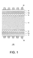
- a photovoltaic device 100 comprises a semiconductor substrate 10, an i-type amorphous layer 12i, a p-type amorphous layer 12p, a transparent conductive layer 14, an i-type amorphous layer 16i, an n-type amorphous layer 16n, a transparent conductive layer 18, and collecting electrodes 20 and 22.
- a structure of the photovoltaic device 100 will now be described while showing a method of producing the photovoltaic device 100.
- TABLE 1 shows example formation conditions of amorphous layers in the photovoltaic device 100.
- the film formation conditions used in the present embodiment are merely exemplary, and may be suitably changed and optimized according to the device to be used.
- the semiconductor substrate 10 comprises a crystalline semiconductor material.
- the semiconductor substrate 10 may be a crystalline semiconductor substrate of an n-type conductivity or a p-type conductivity.
- a monocrystalline silicon substrate for example, a monocrystalline silicon substrate, a polycrystalline silicon substrate, a gallium arsenide substrate (GaAs), an indium phosphide substrate (InP) or the like may be employed.
- the semiconductor substrate 10 absorbs incident light and produces carrier pairs of electrons and holes through photoelectric conversion. In the following description, an example configuration will be described in which an n-type monocrystalline silicon substrate is used as the semiconductor substrate 10.
- the semiconductor substrate 10 is placed in a film formation chamber after being cleaned.
- the cleaning of the semiconductor substrate 10 can be performed using an etchant of hydrofluoric acid (HF etchant) or an RCA cleaning solution.
- a texture structure may be preferably formed on a front surface or a back surface of the semiconductor substrate 10 using alkaline etchant such as a potassium hydroxide etchant (KOH etchant).
- KOH etchant potassium hydroxide etchant
- the semiconductor substrate 10 having the (100) -plane may be anisotropically etched using the KOH etchant, to form a texture structure having a pyramid type (111)-plane.
- a predetermined oxidization process may be applied before the formation of the i-type amorphous layer 12i to form an oxidized interface.
- the substrate may be placed in an atmospheric air environment or in a humidity-controlled atmosphere for a predetermined period of time, or an ozone water process, a hydrogen peroxide water process, an ozonizer process, or the like may be suitably employed.
- the i-type amorphous layer 12i which is an amorphous semiconductor layer is formed over a front surface of the semiconductor substrate 10.
- the i-type amorphous layer 12i is an intrinsic hydrogenated amorphous silicon.
- an intrinsic semiconductor layer refers to a semiconductor layer with a concentration of contained p-type or n-type dopant of less than or equal to 5 x 10 18 /cm 3 , or, when the p-type dopant and the n-type dopant are both contained, a semiconductor layer with a difference of the dopant concentrations of the p-type and n-type of less than or equal to 5 x 10 18 /cm 3 .
- the i-type amorphous layer 12i is preferably formed sufficiently thin to inhibit absorption of the light as much as possible and at the same time, sufficiently thick for passivation of the front surface of the semiconductor substrate 10.
- the thickness of the i-type amorphous layer 12i is preferably in a range of greater than or equal to 1 nm and less than or equal to 25 nm, and more preferably in a range of greater than or equal to 5 nm and less than or equal to 10 nm.
- the i-type amorphous layer 12i can be formed through plasma-enhanced chemical vapor deposition (PECVD), Cat-CVD (Catalytic Chemical Vapor Deposition), sputtering, or the like.
- PECVD plasma-enhanced chemical vapor deposition
- Cat-CVD Catalytic Chemical Vapor Deposition
- sputtering or the like.
- PECVD any of RF plasma CVD, VHF plasma CVD having a high frequency, microwave plasma CVD, or the like may be employed. In the present embodiment, a configuration using the RF plasma CVD will be described.
- the i-type amorphous layer 12i can be formed by supplying a silicon-containing gas such as silane (SiH 4 ) diluted by hydrogen, which is turned into plasma by added RF high-frequency electric power to a parallel-plate electrode or like, to a film formation surface of the semiconductor substrate 10 which is heated.
- gas containing oxygen (O 2 ) is simultaneously introduced at an initial stage of the formation of the i-type amorphous layer 12i, to introduce oxygen to a region near the interface between the semiconductor substrate 10 and the i-type amorphous layer 12i.
- the gas containing oxygen (O 2 ) may be, for example, carbon dioxide (CO 2 ) gas and oxygen (O 2 ).
- a substrate temperature during the film formation is set in a range of higher than or equal to 150 °C and lower than or equal to 250 °C, and an RF power density is set in a range of greater than or equal to 1 mW/cm 2 and less than or equal to 10 mW/cm 2 .
- an oxygen concentration profile is employed in the i-type amorphous layer 12i in which the oxygen concentration is reduced in a step-shape from a region near the interface between the semiconductor substrate 10 and the i-type amorphous layer 12i along the thickness direction of the i-type amorphous layer 12i.
- a flow rate of the oxygen-containing gas is changed in a step-shape during the formation of the i-type amorphous layer 12i, to form a high-oxygen-concentration region containing a large amount of oxygen only on the side of the interface with the semiconductor substrate 10.
- the oxygen concentration in the high-oxygen-concentration region is preferably set in a range of greater than or equal to approximately 1 x 10 20 /cm 3 and less than or equal to 1 x 10 21 /cm 3 , and the oxygen concentration in regions of the i-type amorphous layer 12i other than the high-oxygen-concentration region is preferably set to be less than approximately 1 x 10 20 /cm 3 .
- a step-shaped profile having one or more steps of oxygen concentrations along the thickness direction is preferably employed. This oxygen concentration profile from the semiconductor substrate 10 and characteristics of the photovoltaic device will be described later.
- Concentrations of various elements in a semiconductor film can be measured through secondary ion mass spectrometry (SIMS) or the like.
- SIMS secondary ion mass spectrometry
- the concentrations of various elements in the film can be measured by a method in which the resolution in the thickness direction is not reduced by the texture.
- the p-type amorphous layer 12p is a layer comprising an amorphous semiconductor film containing a dopant of a p-type conductivity.
- the p-type amorphous layer 12p is formed by hydrogenated amorphous silicon.
- the p-type amorphous layer 12p has a higher concentration of the p-type dopant in the film than that of the i-type amorphous layer 12i.
- the p-type amorphous layer 12p preferably has a concentration of the p-type dopant of greater than or equal to 1 x 10 20 /cm 3 .
- a thickness of the p-type amorphous layer 12p is preferably sufficiently thin to inhibit absorption of the light as much as possible, and at the same time, sufficiently thick to efficiently separate carriers generated in the semiconductor substrate 10 at the pn junction and to effectively collect the generated carriers in the transparent conductive layer 14.
- the thickness of the p-type amorphous layer 12p is preferably set in a range of greater than or equal to 1 nm and less than or equal to 10 nm.
- the p-type amorphous layer 12p can also be formed through PECVD, Cat-CVD, sputtering, or the like.
- PECVD RF plasma CVD may be applied.
- the p-type amorphous layer 12p can be formed by supplying a silicon-containing gas such as silane (SiH 4 ) and a p-type dopant-containing gas such as diborane (B 2 H 6 ) diluted by hydrogen, which is turned into plasma by applying RF high-frequency electric power to a parallel-plate electrode or like, over the i-type amorphous layer 12i of the semiconductor substrate 10 which is heated.
- a silicon-containing gas such as silane (SiH 4 )
- a p-type dopant-containing gas such as diborane (B 2 H 6 ) diluted by hydrogen
- diborane (B 2 H 6 ) is diluted with hydrogen in a percentage of 1%.
- a substrate temperature during the film formation is preferably set in a range of higher than or equal to 150 °C and lower than or equal to 250 °C, and an RF power density is preferably set in a range of greater than or equal to 1 mW/cm 2 and less than or equal to 10 mW/cm 2 .
- the i-type amorphous layer 16i is formed over a back surface of the semiconductor substrate 10. Specifically, after the i-type amorphous layer 12i and the p-type amorphous layer 12p are formed, the semiconductor substrate 10 is flipped to turn the front and back sides over, and the i-type amorphous layer 16i is formed over the back surface of the semiconductor substrate 10.
- the i-type amorphous layer 16i is an intrinsic hydrogenated amorphous silicon semiconductor layer.
- a thickness of the i-type amorphous layer 16i is preferably in a range of greater than or equal to 1 nm and less than or equal to 25 nm, and more preferably in a range of greater than or equal to 5 nm and less than or equal to 10 nm.
- the i-type amorphous layer 16i can be formed through PECVD, Cat-CVD, sputtering, or the like.
- PECVD RF plasma CVD may be employed.
- the i-type amorphous layer 16i can be formed by supplying a silicon-containing gas such as silane (SiH 4 ) diluted by hydrogen, which is turned into plasma by applying RF high-frequency electric power to a parallel-plate electrode or like, to a film formation surface of the semiconductor substrate 10 which is heated.
- a substrate temperature during the film formation is preferably set in a range of higher than or equal to 150 °C and lower than or equal to 250 °C, and an RF power density is preferably set in a range of greater than or equal to 1 mW/cm 2 and less than or equal to 10 mW/cm 2 .
- gas containing oxygen is preferably simultaneously introduced during an initial stage of the film formation, to introduce oxygen in a region near an interface between the semiconductor substrate 10 and the i-type amorphous layer 16i.
- the n-type amorphous layer 16n is a layer of an amorphous semiconductor film containing a dopant of an n-type conductivity.
- the n-type amorphous layer 16n is formed by hydrogenated amorphous silicon.
- the n-type amorphous layer 16n is set to have a higher concentration of the n-type dopant in the film than that of the i-type amorphous layer 16i.
- the n-type amorphous layer 16n preferably has a concentration of the n-type dopant of greater than or equal to 1 x 10 20 /cm 3 .
- a thickness of the n-type amorphous layer 16n is preferably sufficiently thin to inhibit absorption of the light as much as possible, and sufficiently thick to effectively separate the carriers generated in the semiconductor substrate 10 by a BSF (Back Surface Field) structure and to efficiently collect the generated carriers in the transparent conductive layer 18.
- the thickness of the n-type amorphous layer 16n is preferably in a range of greater than or equal to 1 nm and less than or equal to 10 nm.
- the n-type amorphous layer 16n can also be formed through PECVD, Cat-CVD, sputtering, or the like.
- PECVD RF plasma CVD may be employed.
- the n-type amorphous layer 16n can be formed by supplying a silicon-containing gas such as silane (SiH 4 ) and an n-type dopant-containing gas such as phosphine (PH 3 ) diluted by hydrogen, which is turned into plasma by applying RF high-frequency electric power to a parallel-plate electrode or like, over the i-type amorphous layer 16i of the semiconductor substrate 10 which is heated.
- a silicon-containing gas such as silane (SiH 4 )
- an n-type dopant-containing gas such as phosphine (PH 3 ) diluted by hydrogen
- phosphine (PH 3 ) is diluted with hydrogen with a percentage of 2%.
- a substrate temperature during the film formation is preferably set in a range of higher than or equal to 150 °C and lower than or equal to 250 °C, and an RF power density is preferably set in a range of greater than or equal to 1 mW/cm 2 and less than or equal to 10 mW/cm 2 .
- a front surface side or to set a back surface side of the semiconductor substrate 10 is a light-receiving surface (a surface through which the light is mainly introduced from the outside).
- the semiconductor substrate 10 is flipped and the i-type amorphous layer 16i and the n-type amorphous layer 16n on the back surface side are formed, but the order of formation of these layers is also arbitrary.
- the transparent conductive layers 14 and 18 are formed over the p-type amorphous layer 12p and the n-type amorphous layer 16n, respectively.
- the transparent conductive layers 14 and 18 are formed, for example, including at least one of metal oxides having a polycrystalline structure, such as indium oxide (In 2 O 3 ), zinc oxide (ZnO), tin oxide (SnO 2 ), and titanium oxide (TiO 2 ), and the metal oxide may be doped with a dopant such as tin (Sn), zinc (Zn), tungsten (W), antimony (Sb), titanium (Ti), cerium (Ce), and gallium (Ga).
- metal oxides having a polycrystalline structure such as indium oxide (In 2 O 3 ), zinc oxide (ZnO), tin oxide (SnO 2 ), and titanium oxide (TiO 2 )
- the metal oxide may be doped with a dopant such as tin (Sn), zinc (Zn), tungsten (W),
- the transparent conductive layers 14 and 18 may be formed through a thin film formation method such as deposition, plasma-enhanced chemical vapor deposition (PECVD), and sputtering. Thicknesses of the transparent conductive layers 14 and 18 can be suitably adjusted according to the indices of refraction of the transparent conductive layers 14 and 18, and in the present embodiment, the thicknesses are set in a range of greater than or equal to 70 nm and less than or equal to 100 nm.
- PECVD plasma-enhanced chemical vapor deposition
- the collecting electrodes 20 and 22 are formed over the transparent conductive layers 14 and 18, respectively.
- the collecting electrodes 20 and 22 preferably have a comb-shaped finger electrode structure.
- the collecting electrodes 20 and 22 can be formed through screen printing, coating, or the like.
- the collecting electrodes 20 and 22 are formed, for example, by applying a silver paste or the like to a thickness of a few tens of ⁇ m.
- a photovoltaic device which was formed similar to the Example except that the oxygen-containing gas such as carbon dioxide gas was not introduced is set as a Comparative Example 1.
- a photovoltaic device in which carbonic gas was introduced over the entire period of formation of the i-type amorphous layer 12i and the i-type amorphous layer 16i, so that the entire regions of the i-type amorphous layer 12i and the i-type amorphous layer 16i contain oxygen is set as a Comparative Example 2.
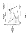
- FIG. 2 shows the concentration profile of oxygen atoms in the films for the semiconductor substrate 10, the i-type amorphous layer 12i, and the p-type amorphous layer 12p in the Example and in the Comparative Examples 1, 2, and 3.
- the concentration profiles of oxygen atoms in the film for the semiconductor substrate 10, the i-type amorphous layer 16i, and the n-type amorphous layer 16n were similar.
- a measurement result for the Example is shown with a solid line and the measurement results for the Comparative Examples 1, 2, and 3 are shown with a dot-and-chain line, a broken line, and a two-dots-and-chain line, respectively.
- oxygen-containing gas such as carbon dioxide gas
- the oxygen-containing gas such as carbon dioxide gas
- the p-type amorphous layer 12p such as in the case of the photovoltaic device of the Comparative Example 1
- oxygen atoms existed in the order of 10 21 /cm 3 at the interface region between the semiconductor substrate 10 and the i-type amorphous layer 12i. This is because the surface of the semiconductor substrate 10 is naturally oxidized in a transportation period from cleaning to the formation processes of the i-type amorphous layer 12i and also in the film formation device.
- the oxygen atoms are also caused due to this process.
- the oxygen concentrations of the i-type amorphous layer 12i and the p-type amorphous layer 12p showed a profile having a peak at the interface with the semiconductor substrate 10, which is reduced to the background level in the i-type amorphous layer 12i, and again increased toward the p-type amorphous layer 12p and the surface.
- the increase in the oxygen concentration in the p-type amorphous layer 12p can be considered to be an influence of introduction of the doping gas and an influence on the surface condition in the measurement.
- oxygen-containing gas was introduced to the entire region of the i-type amorphous layer 12i, such as in the case of the photovoltaic device of the Comparative Example 2
- oxygen existed in a concentration of greater than or equal to approximately 1 x 10 20 /cm 3 in the i-type amorphous layer 12i.
- oxygen existed in a concentration of greater than or equal to approximately 1 x 10 20 /cm 3 in the i-type amorphous layer 12i.
- the oxygen concentration was slightly higher in the Comparative Example 3 than in the Comparative Example 2.
- the i-type amorphous layer 12i was formed while controlling introduction of the oxygen-containing gas in steps, a region containing a large amount of oxygen (high-oxygen-concentration region) near the interface with the semiconductor substrate 10 was observed in a range of less than or equal to 5 nm from the interface with the semiconductor substrate 10.
- the oxygen concentration in the high-oxygen-concentration region was in a range of greater than or equal to approximately 1 x 10 20 /cm 3 and less than or equal to 1 x 10 21 /cm 3 .
- the oxygen concentration in regions other than the high-oxygen-concentration region was less than approximately 1 x 10 21 /cm 3 .
- the high-oxygen-concentration region had a profile of a step-shape having one or more steps of oxygen concentrations along the thickness direction.
- the oxygen concentration profile near the interface with the semiconductor substrate 10 in the i-type amorphous layer 12i had one or more points of inflection, and had regions having different slopes.
- a point A which is at the interface between the semiconductor substrate 10 and the i-type amorphous layer 12i and having an oxygen concentration in the order of 10 21 /cm 3
- a point B in the i-type amorphous layer 12i and in a range of about 1 nm from the interface between the semiconductor substrate 10 and the i-type amorphous layer 12i, and having an oxygen concentration in a range of greater than or equal to approximately 1 x 10 20 /cm 3 and less than or equal to 1 x 10 21 /cm 3
- the oxygen concentration of approximately 1 x 10 20 /cm 3 technically has the following critical meaning. Because the density of the silicon atoms in the i-type amorphous layer 12i is approximately 5 x 10 22 /cm 3 , when the oxygen concentration is approximately 1 x 10 20 /cm 3 , the concentration ratio of the oxygen atoms with respect to the silicon atoms is 0.002. With a value near this value as a boundary, it can be considered that when the oxygen concentration is lower than 0.002, the oxygen atoms act as impurities in silicon, and when the oxygen concentration is higher than 0.002, the oxygen atoms are alloyed with silicon and the film has properties as a compound of oxygen and silicon.
- the properties of the i-type amorphous layer 12i can be considered to change with the boundary at the oxygen concentration of approximately 1 x 10 20 /cm 3 .
- the amorphous layer 12i containing oxygen in the concentration according to the present embodiment is substantially intrinsic.
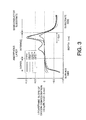
- FIG. 3 shows a slope profile, shown in a logarithmic scale, of the oxygen concentration obtained by differentiating the oxygen concentration profile of FIG. 2 in the thickness direction.
- the Example is shown with a solid line and the Comparative Examples 1, 2, and 3 are shown with a dot-and-chain line, a broken line, and a dotted line, respectively.
- the oxygen concentration profile changes gradually in a large portion in the i-type amorphous layer 12i, and has a steep peak at the interface between the semiconductor layer 10 and the i-type amorphous layer 12i. Therefore, the oxygen concentration slope had a value close to 0 in the i-type amorphous layer 12i and in the p-type amorphous layer 12p except for the region near the interface between the semiconductor substrate 10 and the i-type amorphous layer 12i.
- the slope was rapidly increased from a point which is a few nm away from the interface between the semiconductor substrate 10 and the i-type amorphous layer 12i, the slope became 0 near the interface, and became a negative value in the semiconductor substrate 10.
- the slope was increased from a shallow position in the i-type amorphous layer 12i and showed a peak. The slope then became gradual and approaches 0, and the slope was again increased from a point distanced from the interface between the semiconductor substrate 10 and the i-type amorphous layer 12i by a fewnm.
- the profile of the slope of the oxygen concentration had at least two peaks within the i-type amorphous layer 12i.
- TABLE 2 shows output characteristics of photovoltaic devices of the Example and the Comparative Examples 1 to 3. Measured data were an open-circuit voltage (Voc), a short-circuit current (Isc), a fill factor (FF), and an output power (Pmax). In TABLE 2, normalized values which were normalized against the values in the Comparative Example 1 as 1 are shown.
- the short-circuit current Isc was higher in the Example and in the Comparative Examples 2 and 3 compared with the Comparative Example 1. Specifically, an improvement of 0.5% - 1% was observed. This can be deduced to be caused by the fact that, because the oxygen concentration is higher in the i-type amorphous layers 12i and 16i in regions near the interfaces with the semiconductor substrate 10 in the Example and in the Comparative Examples 2 and 3 compared with the Comparative Example 1, optical bandgaps in these regions of the i-type amorphous layers 12i and 16i were widened and the light transmittance was increased, and consequently, the amount of transmission of light to the semiconductor substrate 10 which is the carrier generation layer was increased and the short-circuit current Isc was increased.
- the output power Pmax was maximum in the Example.
- the open-circuit voltage Voc and the short-circuit current Isc were improved, and with inhibition of the reduction of the fill factor FF, the power generation efficiency was improved.
- oxygen concentrations at point B and point C in FIG. 2 were set to be greater than or equal to 1 x 10 20 /cm 3 and less than or equal to 1 x 10 21 /cm 3 .
- a photovoltaic device in which the oxygen concentrations at point B and point C in FIG. 2 were set to be greater than 1 x 10 21 /cm 3 was set as a Comparative Example 4, and a photovoltaic device in which the oxygen concentrations at point B and point C were set to be less than 1 x 10 20 /cm 3 was set as a Comparative Example 5.
- TABLE 3 shows output characteristics of the photovoltaic devices of the Example and the Comparative Examples 4 and 5. Similar to TABLE 2, the measured data were open-circuit voltage (Voc), short-circuit current (Isc), fill factor (FF), and output power (Pmax), and normalized values which are normalized against the values of the Example as 1 are shown.
- Voc open-circuit voltage
- Isc short-circuit current
- FF fill factor
- Pmax output power
- the Example has the optimum oxygen concentration profile, and the advantage of the improvement of the open-circuit voltage Voc cannot be improved even when oxygen atoms are contained in an amount greater than the optimum amount.
- elements other than oxygen contained in the oxygen-containing gas for example, carbon in the case where carbon dioxide gas is used
Landscapes
- Photovoltaic Devices (AREA)
- Life Sciences & Earth Sciences (AREA)
- Engineering & Computer Science (AREA)
- Sustainable Energy (AREA)
- Sustainable Development (AREA)
Abstract
Description
- The present invention relates to a photovoltaic device.
- Photovoltaic devices are known in which an amorphous silicon layer which is substantially intrinsic is formed between a crystalline silicon substrate and a doped amorphous silicon layer.
- As a means for improving an output characteristic of the photovoltaic device having such a structure, a structure is known in which an oxygen concentration of an interface portion between the silicon substrate and the intrinsic amorphous silicon layer is increased (refer to Japanese Patent No.
4070483 JP 2008-235400 A - On the other hand, it has been reported that in an inactivation technique of a surface of a silicon substrate by the intrinsic amorphous silicon layer, by containing oxygen in an appropriate amount in the entirety of the intrinsic amorphous silicon layer and forming a very small amorphous silicon oxide region within the layer, it is possible to promote the inactivation (refer to J. Appl. Phys. 107, 014504 (2010)). In addition, it has been reported that by containing oxygen in an appropriate amount in the entirety of the intrinsic amorphous silicon layer, the output characteristic of the photovoltaic device can be improved (refer to Appl. Phys. Lett. 91, 133508 (2007).
- When excessive oxygen is introduced into the amorphous silicon layer, the oxygen may act as an impurity to form a defect or form a high-resistance region. Therefore, optimization of the oxygen concentration to be contained is desired. However, the optimum oxygen concentration profile in the intrinsic amorphous silicon layer, in particular, the oxygen concentration at the side of the interface between the silicon substrate and the intrinsic amorphous silicon layer, has not been sufficiently investigated.
- According to one aspect of the present invention, there is provided a photovoltaic device comprising: a crystalline semiconductor substrate of a first conductive type; a first amorphous semiconductor layer which is intrinsic and formed over a first surface of the semiconductor substrate; and a second amorphous semiconductor layer of the first conductive type or of a conductive type opposite to the first conductive type and formed over the first amorphous semiconductor layer, wherein the first amorphous semiconductor layer has an oxygen concentration profile in which a concentration is reduced in a step-shape from a region near an interface with the semiconductor substrate and along a thickness direction.
- According to various aspects of the present invention, a photovoltaic efficiency in the photovoltaic device can be improved.
-
-
FIG. 1 is a cross-sectional diagram of a photovoltaic device according to a preferred embodiment of the present invention. -
FIG. 2 is a diagram showing an oxygen concentration profile of a photovoltaic device according to a preferred embodiment of the present invention. -
FIG. 3 is a diagram showing a slope profile in a logarithmic scale of an oxygen concentration of a photovoltaic device according to a preferred embodiment of the present invention. - As shown in a cross-sectional diagram of
FIG. 1 , aphotovoltaic device 100 according to a preferred embodiment of the present invention comprises asemiconductor substrate 10, an i-typeamorphous layer 12i, a p-typeamorphous layer 12p, a transparentconductive layer 14, an i-typeamorphous layer 16i, an n-typeamorphous layer 16n, a transparentconductive layer 18, and collectingelectrodes - A structure of the
photovoltaic device 100 will now be described while showing a method of producing thephotovoltaic device 100. TABLE 1 shows example formation conditions of amorphous layers in thephotovoltaic device 100. The film formation conditions used in the present embodiment are merely exemplary, and may be suitably changed and optimized according to the device to be used.[TABLE 1] PROCESS SUBSTRATE TEMPERATURE [°C] GAS PRESSURE [Pa] POWER DENSITY [mW/cm2] FRONT SURFACE HYDROGEN TREATMENT 150∼200 H2 : 40sccm 50 2∼4 i-TYPE AMORPHOUS LAYER 12i150∼200 H2 : 200sccm 50 2∼4 SiH4 : 20sccm CO2 : 0∼ 20sccm p-TYPE AMORPHOUS LAYER 12p150∼200 H2 : 200sccm 50 2∼4 SiH4 : 20sccm B2H6 : 20sccm BACK SURFACE HYDROGEN TREATMENT 150∼200 H2:40sccm 50 2∼4 i-TYPE AMORPHOUS LAYER 16i150∼200 H2 : 200sccm 50 2∼4 SiH4 : 20sccm CO2 : 0∼ 20sccm n-TYPE AMORPHOUS LAYER 16n150∼200 H2 : 200sccm 50 2∼4 SiH4 : 20sccm PH3 : 20sccm - The
semiconductor substrate 10 comprises a crystalline semiconductor material. Thesemiconductor substrate 10 may be a crystalline semiconductor substrate of an n-type conductivity or a p-type conductivity. As thesemiconductor substrate 10, for example, a monocrystalline silicon substrate, a polycrystalline silicon substrate, a gallium arsenide substrate (GaAs), an indium phosphide substrate (InP) or the like may be employed. Thesemiconductor substrate 10 absorbs incident light and produces carrier pairs of electrons and holes through photoelectric conversion. In the following description, an example configuration will be described in which an n-type monocrystalline silicon substrate is used as thesemiconductor substrate 10. - The
semiconductor substrate 10 is placed in a film formation chamber after being cleaned. The cleaning of thesemiconductor substrate 10 can be performed using an etchant of hydrofluoric acid (HF etchant) or an RCA cleaning solution. Alternatively, a texture structure may be preferably formed on a front surface or a back surface of thesemiconductor substrate 10 using alkaline etchant such as a potassium hydroxide etchant (KOH etchant). In this case, thesemiconductor substrate 10 having the (100) -plane may be anisotropically etched using the KOH etchant, to form a texture structure having a pyramid type (111)-plane. - Alternatively, a predetermined oxidization process may be applied before the formation of the i-type
amorphous layer 12i to form an oxidized interface. As the predetermined oxidation process, for example, the substrate may be placed in an atmospheric air environment or in a humidity-controlled atmosphere for a predetermined period of time, or an ozone water process, a hydrogen peroxide water process, an ozonizer process, or the like may be suitably employed. - The i-type
amorphous layer 12i which is an amorphous semiconductor layer is formed over a front surface of thesemiconductor substrate 10. For example, the i-typeamorphous layer 12i is an intrinsic hydrogenated amorphous silicon. Here, an intrinsic semiconductor layer refers to a semiconductor layer with a concentration of contained p-type or n-type dopant of less than or equal to 5 x 10¹⁸ /cm3, or, when the p-type dopant and the n-type dopant are both contained, a semiconductor layer with a difference of the dopant concentrations of the p-type and n-type of less than or equal to 5 x 10¹⁸ /cm3. The i-typeamorphous layer 12i is preferably formed sufficiently thin to inhibit absorption of the light as much as possible and at the same time, sufficiently thick for passivation of the front surface of thesemiconductor substrate 10. The thickness of the i-typeamorphous layer 12i is preferably in a range of greater than or equal to 1 nm and less than or equal to 25 nm, and more preferably in a range of greater than or equal to 5 nm and less than or equal to 10 nm. - The i-type
amorphous layer 12i can be formed through plasma-enhanced chemical vapor deposition (PECVD), Cat-CVD (Catalytic Chemical Vapor Deposition), sputtering, or the like. For the PECVD, any of RF plasma CVD, VHF plasma CVD having a high frequency, microwave plasma CVD, or the like may be employed. In the present embodiment, a configuration using the RF plasma CVD will be described. For example, as shown in TABLE 1, the i-typeamorphous layer 12i can be formed by supplying a silicon-containing gas such as silane (SiH4) diluted by hydrogen, which is turned into plasma by added RF high-frequency electric power to a parallel-plate electrode or like, to a film formation surface of thesemiconductor substrate 10 which is heated. In this process, in the present embodiment, gas containing oxygen (O2) is simultaneously introduced at an initial stage of the formation of the i-typeamorphous layer 12i, to introduce oxygen to a region near the interface between thesemiconductor substrate 10 and the i-typeamorphous layer 12i. The gas containing oxygen (O2) may be, for example, carbon dioxide (CO2) gas and oxygen (O2). A substrate temperature during the film formation is set in a range of higher than or equal to 150 °C and lower than or equal to 250 °C, and an RF power density is set in a range of greater than or equal to 1 mW/cm2 and less than or equal to 10 mW/cm2. - As shown in
FIG. 2 , an oxygen concentration profile is employed in the i-typeamorphous layer 12i in which the oxygen concentration is reduced in a step-shape from a region near the interface between thesemiconductor substrate 10 and the i-typeamorphous layer 12i along the thickness direction of the i-typeamorphous layer 12i. For example, a flow rate of the oxygen-containing gas is changed in a step-shape during the formation of the i-typeamorphous layer 12i, to form a high-oxygen-concentration region containing a large amount of oxygen only on the side of the interface with thesemiconductor substrate 10. The oxygen concentration in the high-oxygen-concentration region is preferably set in a range of greater than or equal to approximately 1 x 10²⁰ /cm3 and less than or equal to 1 x 10²¹ /cm3, and the oxygen concentration in regions of the i-typeamorphous layer 12i other than the high-oxygen-concentration region is preferably set to be less than approximately 1 x 10²⁰ /cm3. In addition, in the high-oxygen-concentration region, a step-shaped profile having one or more steps of oxygen concentrations along the thickness direction is preferably employed. This oxygen concentration profile from thesemiconductor substrate 10 and characteristics of the photovoltaic device will be described later. - Concentrations of various elements in a semiconductor film can be measured through secondary ion mass spectrometry (SIMS) or the like. When the texture structure is provided in the
semiconductor substrate 10, the concentrations of various elements in the film can be measured by a method in which the resolution in the thickness direction is not reduced by the texture. - The p-type
amorphous layer 12p is a layer comprising an amorphous semiconductor film containing a dopant of a p-type conductivity. For example, the p-typeamorphous layer 12p is formed by hydrogenated amorphous silicon. The p-typeamorphous layer 12p has a higher concentration of the p-type dopant in the film than that of the i-typeamorphous layer 12i. For example, the p-typeamorphous layer 12p preferably has a concentration of the p-type dopant of greater than or equal to 1 x 10²⁰ /cm3. A thickness of the p-typeamorphous layer 12p is preferably sufficiently thin to inhibit absorption of the light as much as possible, and at the same time, sufficiently thick to efficiently separate carriers generated in thesemiconductor substrate 10 at the pn junction and to effectively collect the generated carriers in the transparentconductive layer 14. For example, the thickness of the p-typeamorphous layer 12p is preferably set in a range of greater than or equal to 1 nm and less than or equal to 10 nm. - The p-type
amorphous layer 12p can also be formed through PECVD, Cat-CVD, sputtering, or the like. For the PECVD, RF plasma CVD may be applied. For example, as shown in TABLE 1, the p-typeamorphous layer 12p can be formed by supplying a silicon-containing gas such as silane (SiH4) and a p-type dopant-containing gas such as diborane (B2H6) diluted by hydrogen, which is turned into plasma by applying RF high-frequency electric power to a parallel-plate electrode or like, over the i-typeamorphous layer 12i of thesemiconductor substrate 10 which is heated. In TABLE 1, diborane (B2H6) is diluted with hydrogen in a percentage of 1%. A substrate temperature during the film formation is preferably set in a range of higher than or equal to 150 °C and lower than or equal to 250 °C, and an RF power density is preferably set in a range of greater than or equal to 1 mW/cm2 and less than or equal to 10 mW/cm2. - The i-type
amorphous layer 16i is formed over a back surface of thesemiconductor substrate 10. Specifically, after the i-typeamorphous layer 12i and the p-typeamorphous layer 12p are formed, thesemiconductor substrate 10 is flipped to turn the front and back sides over, and the i-typeamorphous layer 16i is formed over the back surface of thesemiconductor substrate 10. For example, the i-typeamorphous layer 16i is an intrinsic hydrogenated amorphous silicon semiconductor layer. Similar to the i-typeamorphous layer 12i, a thickness of the i-typeamorphous layer 16i is preferably in a range of greater than or equal to 1 nm and less than or equal to 25 nm, and more preferably in a range of greater than or equal to 5 nm and less than or equal to 10 nm. - The i-type
amorphous layer 16i can be formed through PECVD, Cat-CVD, sputtering, or the like. For the PECVD, RF plasma CVD may be employed. For example, as shown in TABLE 1, the i-typeamorphous layer 16i can be formed by supplying a silicon-containing gas such as silane (SiH4) diluted by hydrogen, which is turned into plasma by applying RF high-frequency electric power to a parallel-plate electrode or like, to a film formation surface of thesemiconductor substrate 10 which is heated. Similar to the i-typeamorphous layer 12i, a substrate temperature during the film formation is preferably set in a range of higher than or equal to 150 °C and lower than or equal to 250 °C, and an RF power density is preferably set in a range of greater than or equal to 1 mW/cm2 and less than or equal to 10 mW/cm2. - In the i-type
amorphous layer 16i also, similar to the i-typeamorphous layer 12i, gas containing oxygen (O2) is preferably simultaneously introduced during an initial stage of the film formation, to introduce oxygen in a region near an interface between thesemiconductor substrate 10 and the i-typeamorphous layer 16i. - The n-type
amorphous layer 16n is a layer of an amorphous semiconductor film containing a dopant of an n-type conductivity. For example, the n-typeamorphous layer 16n is formed by hydrogenated amorphous silicon. The n-typeamorphous layer 16n is set to have a higher concentration of the n-type dopant in the film than that of the i-typeamorphous layer 16i. For example, the n-typeamorphous layer 16n preferably has a concentration of the n-type dopant of greater than or equal to 1 x 10²⁰ /cm3. A thickness of the n-typeamorphous layer 16n is preferably sufficiently thin to inhibit absorption of the light as much as possible, and sufficiently thick to effectively separate the carriers generated in thesemiconductor substrate 10 by a BSF (Back Surface Field) structure and to efficiently collect the generated carriers in the transparentconductive layer 18. For example, the thickness of the n-typeamorphous layer 16n is preferably in a range of greater than or equal to 1 nm and less than or equal to 10 nm. - The n-type
amorphous layer 16n can also be formed through PECVD, Cat-CVD, sputtering, or the like. For the PECVD, RF plasma CVD may be employed. For example, as shown in TABLE 1, the n-typeamorphous layer 16n can be formed by supplying a silicon-containing gas such as silane (SiH4) and an n-type dopant-containing gas such as phosphine (PH3) diluted by hydrogen, which is turned into plasma by applying RF high-frequency electric power to a parallel-plate electrode or like, over the i-typeamorphous layer 16i of thesemiconductor substrate 10 which is heated. In TABLE 1, phosphine (PH3) is diluted with hydrogen with a percentage of 2%. A substrate temperature during the film formation is preferably set in a range of higher than or equal to 150 °C and lower than or equal to 250 °C, and an RF power density is preferably set in a range of greater than or equal to 1 mW/cm2 and less than or equal to 10 mW/cm2. - It is arbitrary whether to set a front surface side or to set a back surface side of the
semiconductor substrate 10 as a light-receiving surface (a surface through which the light is mainly introduced from the outside). In addition, in the above-described embodiment, after the i-typeamorphous layer 12i and the p-typeamorphous layer 12p on the front surface side are formed, thesemiconductor substrate 10 is flipped and the i-typeamorphous layer 16i and the n-typeamorphous layer 16n on the back surface side are formed, but the order of formation of these layers is also arbitrary. - The transparent
conductive layers amorphous layer 12p and the n-typeamorphous layer 16n, respectively. The transparentconductive layers conductive layers conductive layers conductive layers - The collecting
electrodes conductive layers electrodes electrodes electrodes - A photovoltaic device having an i-type
amorphous layer 12i, having an oxygen concentration profile in which the concentration is reduced in a step-shape from a region near the interface between thesemiconductor substrate 10 and the i-typeamorphous layer 12i along the thickness direction, and an i-typeamorphous layer 16i having an oxygen concentration profile in which the concentration is reduced from a region near the interface between thesemiconductor substrate 10 and the i-typeamorphous layer 16i along the thickness direction, formed through the above-described formation method and under the conditions shown in TABLE 1, is set as the Example. - A photovoltaic device which was formed similar to the Example except that the oxygen-containing gas such as carbon dioxide gas was not introduced is set as a Comparative Example 1. In addition, a photovoltaic device in which carbonic gas was introduced over the entire period of formation of the i-type
amorphous layer 12i and the i-typeamorphous layer 16i, so that the entire regions of the i-typeamorphous layer 12i and the i-typeamorphous layer 16i contain oxygen, is set as a Comparative Example 2. Moreover, a photovoltaic device in which carbon dioxide gas was introduced over the entire period of formation of the i-typeamorphous layer 12i, the p-typeamorphous layer 12p, the i-typeamorphous layer 16i, and the n-typeamorphous layer 16n, so that the entire regions of the i-typeamorphous layer 12i, the p-typeamorphous layer 12p, the i-typeamorphous layer 16i, and the n-typeamorphous layer 16n contain oxygen, is set as a Comparative Example 3. -
FIG. 2 shows the concentration profile of oxygen atoms in the films for thesemiconductor substrate 10, the i-typeamorphous layer 12i, and the p-typeamorphous layer 12p in the Example and in the Comparative Examples 1, 2, and 3. The concentration profiles of oxygen atoms in the film for thesemiconductor substrate 10, the i-typeamorphous layer 16i, and the n-typeamorphous layer 16n were similar. InFIG. 2 , a measurement result for the Example is shown with a solid line and the measurement results for the Comparative Examples 1, 2, and 3 are shown with a dot-and-chain line, a broken line, and a two-dots-and-chain line, respectively. - In the case where the oxygen-containing gas such as carbon dioxide gas is not introduced in the i-type
amorphous layer 12i and the p-typeamorphous layer 12p, such as in the case of the photovoltaic device of the Comparative Example 1, also, oxygen atoms existed in the order of 1021 /cm3 at the interface region between thesemiconductor substrate 10 and the i-typeamorphous layer 12i. This is because the surface of thesemiconductor substrate 10 is naturally oxidized in a transportation period from cleaning to the formation processes of the i-typeamorphous layer 12i and also in the film formation device. Moreover, in a case where a predetermined oxidization process is applied prior to the film formation as described above, the oxygen atoms are also caused due to this process. Because of this, the oxygen concentrations of the i-typeamorphous layer 12i and the p-typeamorphous layer 12p showed a profile having a peak at the interface with thesemiconductor substrate 10, which is reduced to the background level in the i-typeamorphous layer 12i, and again increased toward the p-typeamorphous layer 12p and the surface. The increase in the oxygen concentration in the p-typeamorphous layer 12p can be considered to be an influence of introduction of the doping gas and an influence on the surface condition in the measurement. - In the case where the oxygen-containing gas was introduced to the entire region of the i-type
amorphous layer 12i, such as in the case of the photovoltaic device of the Comparative Example 2, oxygen existed in a concentration of greater than or equal to approximately 1 x 10²⁰ /cm3 in the i-typeamorphous layer 12i. Similarly, in the photovoltaic device of the Comparative Example 3 also, oxygen existed in a concentration of greater than or equal to approximately 1 x 10²⁰ /cm3 in the i-typeamorphous layer 12i. The oxygen concentration was slightly higher in the Comparative Example 3 than in the Comparative Example 2. - On the other hand, in the photovoltaic device of the Example, a peak of the oxygen concentration existed in the interface region with the
semiconductor substrate 10 for a similar reason to that in the Comparative Example 1. However, because the i-typeamorphous layer 12i was formed while controlling introduction of the oxygen-containing gas in steps, a region containing a large amount of oxygen (high-oxygen-concentration region) near the interface with thesemiconductor substrate 10 was observed in a range of less than or equal to 5 nm from the interface with thesemiconductor substrate 10. The oxygen concentration in the high-oxygen-concentration region was in a range of greater than or equal to approximately 1 x 10²⁰ /cm3 and less than or equal to 1 x 10²¹ /cm3. In addition, in the i-typeamorphous layer 12i, the oxygen concentration in regions other than the high-oxygen-concentration region was less than approximately 1 x 10²¹ /cm3. - Moreover, the high-oxygen-concentration region had a profile of a step-shape having one or more steps of oxygen concentrations along the thickness direction. In other words, the oxygen concentration profile near the interface with the
semiconductor substrate 10 in the i-typeamorphous layer 12i had one or more points of inflection, and had regions having different slopes. More specifically, there had been confirmed, as the inflection points, a point A which is at the interface between thesemiconductor substrate 10 and the i-typeamorphous layer 12i and having an oxygen concentration in the order of 1021 /cm3, a point B in the i-typeamorphous layer 12i and in a range of about 1 nm from the interface between thesemiconductor substrate 10 and the i-typeamorphous layer 12i, and having an oxygen concentration in a range of greater than or equal to approximately 1 x 10²⁰ /cm3 and less than or equal to 1 x 10²¹ /cm3, a point C in the i-typeamorphous layer 12i and in an approximate range of greater than or equal to 1 nm and less than or equal to 5 nm from the interface between thesemiconductor substrate 10 and the i-typeamorphous layer 12i, and having an oxygen concentration in a range of greater than or equal to approximately 1 x 10²⁰ /cm3 and less than or equal to 1 x 10²¹ /cm3, and a point D in the i-typeamorphous layer 12i and distanced from the interface between thesemiconductor substrate 10 and the i-typeamorphous layer 12i by about 5 nm and having an oxygen concentration of less than or equal to approximately 1 x 10²⁰ /cm3. Such an oxygen concentration profile was more clearly confirmed when the concentration axis was shown logarithmically. - The oxygen concentration of approximately 1 x 10²⁰ /cm3 technically has the following critical meaning. Because the density of the silicon atoms in the i-type
amorphous layer 12i is approximately 5 x 10²² /cm3, when the oxygen concentration is approximately 1 x 10²⁰ /cm3, the concentration ratio of the oxygen atoms with respect to the silicon atoms is 0.002. With a value near this value as a boundary, it can be considered that when the oxygen concentration is lower than 0.002, the oxygen atoms act as impurities in silicon, and when the oxygen concentration is higher than 0.002, the oxygen atoms are alloyed with silicon and the film has properties as a compound of oxygen and silicon. Therefore, the properties of the i-typeamorphous layer 12i can be considered to change with the boundary at the oxygen concentration of approximately 1 x 10²⁰ /cm3. As the oxygen atoms in the semiconductor layer of the present embodiment have a very low carrier activation percentage, theamorphous layer 12i containing oxygen in the concentration according to the present embodiment is substantially intrinsic. -
FIG. 3 shows a slope profile, shown in a logarithmic scale, of the oxygen concentration obtained by differentiating the oxygen concentration profile ofFIG. 2 in the thickness direction. InFIG. 3 , the Example is shown with a solid line and the Comparative Examples 1, 2, and 3 are shown with a dot-and-chain line, a broken line, and a dotted line, respectively. - In the Comparative Examples 1 - 3, the oxygen concentration profile changes gradually in a large portion in the i-type
amorphous layer 12i, and has a steep peak at the interface between thesemiconductor layer 10 and the i-typeamorphous layer 12i. Therefore, the oxygen concentration slope had a value close to 0 in the i-typeamorphous layer 12i and in the p-typeamorphous layer 12p except for the region near the interface between thesemiconductor substrate 10 and the i-typeamorphous layer 12i. In addition, as the position approaches thesemiconductor substrate 10 from the surface side, the slope was rapidly increased from a point which is a few nm away from the interface between thesemiconductor substrate 10 and the i-typeamorphous layer 12i, the slope became 0 near the interface, and became a negative value in thesemiconductor substrate 10. - On the other hand, in the photovoltaic device of the Example, as the position approaches the
semiconductor substrate 10 from the surface side, the slope was increased from a shallow position in the i-typeamorphous layer 12i and showed a peak. The slope then became gradual and approaches 0, and the slope was again increased from a point distanced from the interface between thesemiconductor substrate 10 and the i-typeamorphous layer 12i by a fewnm. Thus, the profile of the slope of the oxygen concentration had at least two peaks within the i-typeamorphous layer 12i. - The above-described tendency was similarly observed in the concentration profiles of oxygen atoms in the film for the
semiconductor substrate 10, the i-typeamorphous layer 16i, and the n-typeamorphous layer 16n. - TABLE 2 shows output characteristics of photovoltaic devices of the Example and the Comparative Examples 1 to 3. Measured data were an open-circuit voltage (Voc), a short-circuit current (Isc), a fill factor (FF), and an output power (Pmax). In TABLE 2, normalized values which were normalized against the values in the Comparative Example 1 as 1 are shown.
[TABLE 2] OPEN-CIRCUIT VOLTAGE Voc SHORT-CIRCUIT CURRENT Isc FILL FACTOR FF OUTPUT Pmax EXAMPLE 1.01 1.005 1.00 1.015 COMPARATIVE EXAMPLE 1 1.00 1.000 1.00 1.000 COMPARATIVE EXAMPLE 2 1.01 1.005 0.98 0.995 COMPARATIVE EXAMPLE 3 1.01 1.005 0.96 0.975 - An improvement of the open-circuit voltage can be confirmed in the Example and in the Comparative Examples 2 and 3 compared with the Comparative Example 1 in which the oxygen atoms are not intentionally introduced into the i-type
amorphous layers amorphous layers semiconductor substrate 10 in the Example and the Comparative Examples 2 and 3 compared with the Comparative Example 1, defects at the interfaces between thesemiconductor substrate 10 and the i-typeamorphous layers - The short-circuit current Isc was higher in the Example and in the Comparative Examples 2 and 3 compared with the Comparative Example 1. Specifically, an improvement of 0.5% - 1% was observed. This can be deduced to be caused by the fact that, because the oxygen concentration is higher in the i-type
amorphous layers semiconductor substrate 10 in the Example and in the Comparative Examples 2 and 3 compared with the Comparative Example 1, optical bandgaps in these regions of the i-typeamorphous layers semiconductor substrate 10 which is the carrier generation layer was increased and the short-circuit current Isc was increased. - With regard to the fill factor FF, no significant difference was observed between the Comparative Example 1 and the Example. However, in the Comparative Example 2 in which oxygen was intentionally introduced in the entire region of the i-type
amorphous layers amorphous layer 12p and the n-typeamorphous layer 16n, reduction of the fill factor FF was observed compared with the Comparative Example 1 and the Example. This can be deduced as being caused by the fact that when excessive oxygen atoms are contained in the i-typeamorphous layers amorphous layer 12p, and the n-typeamorphous layer 16n, the oxygen atoms may act as an impurity and form defects or acts as an electrically resistive layer. In contrast, as in the Example, when the oxygen was contained in a range of 5 nm from the interfaces between thesemiconductor substrate 10 and the i-typeamorphous layers - As a result of the above described observations, the output power Pmax was maximum in the Example. In other words, it can be deduced that with the reduction of defects near the interface with the
semiconductor substrate 10 and effective introduction of light into thesemiconductor substrate 10, the open-circuit voltage Voc and the short-circuit current Isc were improved, and with inhibition of the reduction of the fill factor FF, the power generation efficiency was improved. - In the Example, oxygen concentrations at point B and point C in
FIG. 2 were set to be greater than or equal to 1 x 10²⁰ /cm3 and less than or equal to 1 x 10²¹ /cm3. A photovoltaic device in which the oxygen concentrations at point B and point C inFIG. 2 were set to be greater than 1 x 10²¹ /cm3 was set as a Comparative Example 4, and a photovoltaic device in which the oxygen concentrations at point B and point C were set to be less than 1 x 10²⁰ /cm3 was set as a Comparative Example 5. - TABLE 3 shows output characteristics of the photovoltaic devices of the Example and the Comparative Examples 4 and 5. Similar to TABLE 2, the measured data were open-circuit voltage (Voc), short-circuit current (Isc), fill factor (FF), and output power (Pmax), and normalized values which are normalized against the values of the Example as 1 are shown.
[TABLE 3] OPEN-CIRCUIT VOLTAGE Voc SHORT-CIRCUIT CURRENT Isc FILL FACTOR FF OUTPUT Pmax EXAMPLE 1.00 1.00 1.00 1.00 COMPARATIVE EXAMPLE 4 1.00 1.01 0.95 0.96 COMPARATIVE EXAMPLE 5 0.98 0.99 1.00 0.97 - Compared with the Example, no significant improvement was observed in the open-circuit voltage Voc for the Comparative Example 4, and a reduction of the open-circuit voltage Voc was observed in the Comparative Example 5. Thus, it can be considered that the Example has the optimum oxygen concentration profile, and the advantage of the improvement of the open-circuit voltage Voc cannot be improved even when oxygen atoms are contained in an amount greater than the optimum amount. In addition, a case may be possible in which elements other than oxygen contained in the oxygen-containing gas (for example, carbon in the case where carbon dioxide gas is used) may be simultaneously introduced into the i-type
amorphous layers - On the other hand, with regard to the fill factor FF, a significant reduction was observed in the Comparative Example 4 compared with the Example. It can be deduced that even when the oxygen is excessively contained only in the range up to 5 nm from the interfaces between the
semiconductor substrate 10 and i-typeamorphous layers - In the embodiment, a configuration is described in which oxygen is introduced to both the i-type
amorphous layer 12i and the i-typeamorphous layer 16i, but a significant advantage can be obtained by introducing oxygen to at least one of the i-typeamorphous layer 12i and the i-typeamorphous layer 16i.
Claims (6)
- A photovoltaic device comprising:a crystalline semiconductor substrate of a first conductive type;a first amorphous semiconductor layer which is intrinsic and formed over a first surface of the semiconductor substrate; anda second amorphous semiconductor layer of the first conductive type of or a conductive type opposite of the first conductive type and formed over the first amorphous semiconductor layer, whereinthe first amorphous semiconductor layer has an oxygen concentration profile in which a concentration is reduced in a step-shape from a region near an interface with the semiconductor substrate and along a thickness direction.
- The photovoltaic device according to Claim 1, wherein
an oxygen concentration in a high-oxygen-concentration region within 5 nm near the interface between the semiconductor substrate and the first amorphous semiconductor layer is greater than or equal to 1 x 10²⁰ /cm3 and less than or equal to 1 x 10²¹ / cm3. - The photovoltaic device according to Claim 2, wherein
an oxygen concentration in regions in the first amorphous semiconductor layer other than the high-oxygen-concentration region is less than 1 x 10²⁰ /cm3. - The photovoltaic device according to Claim 1, further comprising:a third amorphous semiconductor layer which is intrinsic and formed over a second surface, opposite to the first surface, of the semiconductor substrate; anda fourth amorphous semiconductor layer of an opposite conductive type to that of the second amorphous semiconductor layer and formed over the third amorphous semiconductor layer, whereinthe third amorphous semiconductor layer has an oxygen concentration profile in which a concentration is reduced in a step-shape from a region near an interface with the semiconductor substrate and along a thickness direction.
- The photovoltaic device according to Claim 2, further comprising:a third amorphous semiconductor layer which is intrinsic and formed over a second surface, opposite to the first surface, of the semiconductor substrate; anda fourth amorphous semiconductor layer of an opposite conductive type to that of the second amorphous semiconductor layer and formed over the third amorphous semiconductor layer, whereinthe third amorphous semiconductor layer has an oxygen concentration profile in which a concentration is reduced in a step-shape from a region near an interface with the semiconductor substrate and along a thickness direction.
- The photovoltaic device according to Claim 3, further comprising:a third amorphous semiconductor layer which is intrinsic and formed over a second surface, opposite to the first surface, of the semiconductor substrate; anda fourth amorphous semiconductor layer of an opposite conductive type to that of the second amorphous semiconductor layer and formed over the third amorphous semiconductor layer, whereinthe third amorphous semiconductor layer has an oxygen concentration profile in which a concentration is reduced in a step-shape from a region near an interface with the semiconductor substrate and along a thickness direction.
Applications Claiming Priority (2)
| Application Number | Priority Date | Filing Date | Title |
|---|---|---|---|
| JP2011145142A JP5824681B2 (en) | 2011-06-30 | 2011-06-30 | Photovoltaic device |
| PCT/JP2012/057140 WO2013001863A1 (en) | 2011-06-30 | 2012-03-21 | Photo voltaic device |
Publications (3)
| Publication Number | Publication Date |
|---|---|
| EP2728622A1 true EP2728622A1 (en) | 2014-05-07 |
| EP2728622A4 EP2728622A4 (en) | 2014-12-10 |
| EP2728622B1 EP2728622B1 (en) | 2018-05-09 |
Family
ID=47423774
Family Applications (1)
| Application Number | Title | Priority Date | Filing Date |
|---|---|---|---|
| EP12804030.0A Active EP2728622B1 (en) | 2011-06-30 | 2012-03-21 | Photovoltaic device |
Country Status (5)
| Country | Link |
|---|---|
| US (2) | US9337372B2 (en) |
| EP (1) | EP2728622B1 (en) |
| JP (1) | JP5824681B2 (en) |
| CN (1) | CN103608933B (en) |
| WO (1) | WO2013001863A1 (en) |
Families Citing this family (12)
| Publication number | Priority date | Publication date | Assignee | Title |
|---|---|---|---|---|
| EP2822042B1 (en) * | 2012-03-02 | 2016-10-05 | Panasonic Intellectual Property Management Co., Ltd. | Photovoltaic device |
| JP6185304B2 (en) * | 2013-06-28 | 2017-08-23 | 株式会社カネカ | Crystalline silicon photoelectric conversion device and manufacturing method thereof |
| JP6350979B2 (en) * | 2013-09-04 | 2018-07-04 | パナソニックIpマネジメント株式会社 | Solar cell |
| JP6502651B2 (en) * | 2014-11-13 | 2019-04-17 | 信越化学工業株式会社 | Method of manufacturing solar cell and method of manufacturing solar cell module |
| CN104576801B (en) * | 2014-11-27 | 2017-09-01 | 湖南共创光伏科技有限公司 | Compound unijunction PIN solar cells of crystal silicon and silicon thin film with transition zone and preparation method thereof |
| WO2016147566A1 (en) * | 2015-03-17 | 2016-09-22 | パナソニックIpマネジメント株式会社 | Solar battery cell |
| JP6785427B2 (en) * | 2016-02-01 | 2020-11-18 | パナソニックIpマネジメント株式会社 | Solar cell elements and solar cell modules |
| CN112018217B (en) * | 2019-05-29 | 2025-03-18 | 德运创鑫(北京)科技有限公司 | Method for preparing silicon heterojunction solar cell and solar cell thereof |
| JP2022543548A (en) | 2019-08-09 | 2022-10-13 | リーディング エッジ イクウィップメント テクノロジーズ インコーポレイテッド | Wafers with regions of low oxygen concentration |
| WO2021030236A2 (en) | 2019-08-09 | 2021-02-18 | Leading Edge Equipment Technologies, Inc. | Producing a ribbon or wafer with regions of low oxygen concentration |
| CN114220887A (en) * | 2021-12-11 | 2022-03-22 | 中威新能源(成都)有限公司 | Preparation method of heterojunction solar cell, heterojunction solar cell and application |
| CN114709277B (en) | 2022-05-31 | 2022-09-23 | 浙江晶科能源有限公司 | Solar cell, preparation method thereof and photovoltaic module |
Family Cites Families (7)
| Publication number | Priority date | Publication date | Assignee | Title |
|---|---|---|---|---|
| JP2002329878A (en) * | 2001-04-27 | 2002-11-15 | Sharp Corp | Thin film solar cell and method of manufacturing thin film solar cell |
| JP4070483B2 (en) * | 2002-03-05 | 2008-04-02 | 三洋電機株式会社 | Photovoltaic device and manufacturing method thereof |
| JP2004014812A (en) * | 2002-06-07 | 2004-01-15 | Canon Inc | Photovoltaic element |
| JP2005175160A (en) * | 2003-12-10 | 2005-06-30 | Sanyo Electric Co Ltd | Photovoltaic device |
| JP5526461B2 (en) * | 2007-03-19 | 2014-06-18 | 三洋電機株式会社 | Photovoltaic device |
| TW200947725A (en) | 2008-01-24 | 2009-11-16 | Applied Materials Inc | Improved HIT solar cell structure |
| FR2955702B1 (en) * | 2010-01-27 | 2012-01-27 | Commissariat Energie Atomique | PHOTOVOLTAIC CELL COMPRISING A THIN SILICON CRYSTALLINE OXIDE PASSIVATION FILM AND METHOD OF MAKING SAME |
-
2011
- 2011-06-30 JP JP2011145142A patent/JP5824681B2/en active Active
-
2012
- 2012-03-21 WO PCT/JP2012/057140 patent/WO2013001863A1/en not_active Ceased
- 2012-03-21 EP EP12804030.0A patent/EP2728622B1/en active Active
- 2012-03-21 CN CN201280029337.4A patent/CN103608933B/en active Active
-
2013
- 2013-12-19 US US14/134,496 patent/US9337372B2/en active Active
-
2016
- 2016-04-11 US US15/095,530 patent/US10340403B2/en active Active
Also Published As
| Publication number | Publication date |
|---|---|
| US20140102527A1 (en) | 2014-04-17 |
| EP2728622A4 (en) | 2014-12-10 |
| WO2013001863A1 (en) | 2013-01-03 |
| US10340403B2 (en) | 2019-07-02 |
| JP5824681B2 (en) | 2015-11-25 |
| US9337372B2 (en) | 2016-05-10 |
| US20160225929A1 (en) | 2016-08-04 |
| JP2013012621A (en) | 2013-01-17 |
| EP2728622B1 (en) | 2018-05-09 |
| CN103608933B (en) | 2016-03-30 |
| CN103608933A (en) | 2014-02-26 |
Similar Documents
| Publication | Publication Date | Title |
|---|---|---|
| EP2728622B1 (en) | Photovoltaic device | |
| EP2728628B1 (en) | Photovoltaic device | |
| EP2624307B1 (en) | Method for manufacturing photoelectric conversion device | |
| EP2110859B1 (en) | Laminate type photoelectric converter and method for fabricating the same | |
| US9705022B2 (en) | Photovoltaic device | |
| US20110068367A1 (en) | Double-sided heterojunction solar cell based on thin epitaxial silicon | |
| EP2846363A2 (en) | Solar cell | |
| JP5101200B2 (en) | Method for manufacturing photoelectric conversion device | |
| US12635283B2 (en) | Solar cell and method for forming the same | |
| JP2009290115A (en) | Silicon-based thin-film solar battery | |
| JP6206687B2 (en) | Photovoltaic device and manufacturing method thereof | |
| JP6021084B2 (en) | Photovoltaic device and manufacturing method thereof | |
| JP2011171384A (en) | Thin-film photoelectric conversion device | |
| JP2016219854A (en) | Photovoltaic device and manufacturing method of photoelectric conversion device | |
| JP5339294B2 (en) | Method for manufacturing photoelectric conversion device |
Legal Events
| Date | Code | Title | Description |
|---|---|---|---|
| PUAI | Public reference made under article 153(3) epc to a published international application that has entered the european phase |
Free format text: ORIGINAL CODE: 0009012 |
|
| 17P | Request for examination filed |
Effective date: 20140103 |
|
| AK | Designated contracting states |
Kind code of ref document: A1 Designated state(s): AL AT BE BG CH CY CZ DE DK EE ES FI FR GB GR HR HU IE IS IT LI LT LU LV MC MK MT NL NO PL PT RO RS SE SI SK SM TR |
|
| DAX | Request for extension of the european patent (deleted) | ||
| REG | Reference to a national code |
Ref country code: DE Ref legal event code: R079 Ref document number: 602012046221 Country of ref document: DE Free format text: PREVIOUS MAIN CLASS: H01L0031040000 Ipc: H01L0031074700 |
|
| A4 | Supplementary search report drawn up and despatched |
Effective date: 20141112 |
|
| RIC1 | Information provided on ipc code assigned before grant |
Ipc: H01L 31/0747 20120101AFI20141106BHEP Ipc: H01L 31/0376 20060101ALI20141106BHEP Ipc: H01L 31/075 20120101ALI20141106BHEP |
|
| RAP1 | Party data changed (applicant data changed or rights of an application transferred) |
Owner name: PANASONIC INTELLECTUAL PROPERTY MANAGEMENT CO., LT |
|
| GRAP | Despatch of communication of intention to grant a patent |
Free format text: ORIGINAL CODE: EPIDOSNIGR1 |
|
| STAA | Information on the status of an ep patent application or granted ep patent |
Free format text: STATUS: GRANT OF PATENT IS INTENDED |
|
| INTG | Intention to grant announced |
Effective date: 20171121 |
|
| GRAS | Grant fee paid |
Free format text: ORIGINAL CODE: EPIDOSNIGR3 |
|
| GRAA | (expected) grant |
Free format text: ORIGINAL CODE: 0009210 |
|
| STAA | Information on the status of an ep patent application or granted ep patent |
Free format text: STATUS: THE PATENT HAS BEEN GRANTED |
|
| AK | Designated contracting states |
Kind code of ref document: B1 Designated state(s): AL AT BE BG CH CY CZ DE DK EE ES FI FR GB GR HR HU IE IS IT LI LT LU LV MC MK MT NL NO PL PT RO RS SE SI SK SM TR |
|
| REG | Reference to a national code |
Ref country code: GB Ref legal event code: FG4D |
|
| REG | Reference to a national code |
Ref country code: CH Ref legal event code: EP Ref country code: AT Ref legal event code: REF Ref document number: 998304 Country of ref document: AT Kind code of ref document: T Effective date: 20180515 |
|
| REG | Reference to a national code |
Ref country code: IE Ref legal event code: FG4D |
|
| REG | Reference to a national code |
Ref country code: DE Ref legal event code: R096 Ref document number: 602012046221 Country of ref document: DE |
|
| REG | Reference to a national code |
Ref country code: NL Ref legal event code: MP Effective date: 20180509 |
|
| REG | Reference to a national code |
Ref country code: LT Ref legal event code: MG4D |
|
| PG25 | Lapsed in a contracting state [announced via postgrant information from national office to epo] |
Ref country code: SE Free format text: LAPSE BECAUSE OF FAILURE TO SUBMIT A TRANSLATION OF THE DESCRIPTION OR TO PAY THE FEE WITHIN THE PRESCRIBED TIME-LIMIT Effective date: 20180509 Ref country code: LT Free format text: LAPSE BECAUSE OF FAILURE TO SUBMIT A TRANSLATION OF THE DESCRIPTION OR TO PAY THE FEE WITHIN THE PRESCRIBED TIME-LIMIT Effective date: 20180509 Ref country code: ES Free format text: LAPSE BECAUSE OF FAILURE TO SUBMIT A TRANSLATION OF THE DESCRIPTION OR TO PAY THE FEE WITHIN THE PRESCRIBED TIME-LIMIT Effective date: 20180509 Ref country code: NO Free format text: LAPSE BECAUSE OF FAILURE TO SUBMIT A TRANSLATION OF THE DESCRIPTION OR TO PAY THE FEE WITHIN THE PRESCRIBED TIME-LIMIT Effective date: 20180809 Ref country code: FI Free format text: LAPSE BECAUSE OF FAILURE TO SUBMIT A TRANSLATION OF THE DESCRIPTION OR TO PAY THE FEE WITHIN THE PRESCRIBED TIME-LIMIT Effective date: 20180509 Ref country code: BG Free format text: LAPSE BECAUSE OF FAILURE TO SUBMIT A TRANSLATION OF THE DESCRIPTION OR TO PAY THE FEE WITHIN THE PRESCRIBED TIME-LIMIT Effective date: 20180809 |
|
| PG25 | Lapsed in a contracting state [announced via postgrant information from national office to epo] |
Ref country code: GR Free format text: LAPSE BECAUSE OF FAILURE TO SUBMIT A TRANSLATION OF THE DESCRIPTION OR TO PAY THE FEE WITHIN THE PRESCRIBED TIME-LIMIT Effective date: 20180810 Ref country code: RS Free format text: LAPSE BECAUSE OF FAILURE TO SUBMIT A TRANSLATION OF THE DESCRIPTION OR TO PAY THE FEE WITHIN THE PRESCRIBED TIME-LIMIT Effective date: 20180509 Ref country code: NL Free format text: LAPSE BECAUSE OF FAILURE TO SUBMIT A TRANSLATION OF THE DESCRIPTION OR TO PAY THE FEE WITHIN THE PRESCRIBED TIME-LIMIT Effective date: 20180509 Ref country code: LV Free format text: LAPSE BECAUSE OF FAILURE TO SUBMIT A TRANSLATION OF THE DESCRIPTION OR TO PAY THE FEE WITHIN THE PRESCRIBED TIME-LIMIT Effective date: 20180509 Ref country code: HR Free format text: LAPSE BECAUSE OF FAILURE TO SUBMIT A TRANSLATION OF THE DESCRIPTION OR TO PAY THE FEE WITHIN THE PRESCRIBED TIME-LIMIT Effective date: 20180509 |
|
| REG | Reference to a national code |
Ref country code: AT Ref legal event code: MK05 Ref document number: 998304 Country of ref document: AT Kind code of ref document: T Effective date: 20180509 |
|
| PG25 | Lapsed in a contracting state [announced via postgrant information from national office to epo] |
Ref country code: SK Free format text: LAPSE BECAUSE OF FAILURE TO SUBMIT A TRANSLATION OF THE DESCRIPTION OR TO PAY THE FEE WITHIN THE PRESCRIBED TIME-LIMIT Effective date: 20180509 Ref country code: EE Free format text: LAPSE BECAUSE OF FAILURE TO SUBMIT A TRANSLATION OF THE DESCRIPTION OR TO PAY THE FEE WITHIN THE PRESCRIBED TIME-LIMIT Effective date: 20180509 Ref country code: DK Free format text: LAPSE BECAUSE OF FAILURE TO SUBMIT A TRANSLATION OF THE DESCRIPTION OR TO PAY THE FEE WITHIN THE PRESCRIBED TIME-LIMIT Effective date: 20180509 Ref country code: PL Free format text: LAPSE BECAUSE OF FAILURE TO SUBMIT A TRANSLATION OF THE DESCRIPTION OR TO PAY THE FEE WITHIN THE PRESCRIBED TIME-LIMIT Effective date: 20180509 Ref country code: AT Free format text: LAPSE BECAUSE OF FAILURE TO SUBMIT A TRANSLATION OF THE DESCRIPTION OR TO PAY THE FEE WITHIN THE PRESCRIBED TIME-LIMIT Effective date: 20180509 Ref country code: CZ Free format text: LAPSE BECAUSE OF FAILURE TO SUBMIT A TRANSLATION OF THE DESCRIPTION OR TO PAY THE FEE WITHIN THE PRESCRIBED TIME-LIMIT Effective date: 20180509 Ref country code: RO Free format text: LAPSE BECAUSE OF FAILURE TO SUBMIT A TRANSLATION OF THE DESCRIPTION OR TO PAY THE FEE WITHIN THE PRESCRIBED TIME-LIMIT Effective date: 20180509 |
|
| REG | Reference to a national code |
Ref country code: DE Ref legal event code: R097 Ref document number: 602012046221 Country of ref document: DE |
|
| PG25 | Lapsed in a contracting state [announced via postgrant information from national office to epo] |
Ref country code: SM Free format text: LAPSE BECAUSE OF FAILURE TO SUBMIT A TRANSLATION OF THE DESCRIPTION OR TO PAY THE FEE WITHIN THE PRESCRIBED TIME-LIMIT Effective date: 20180509 |
|
| PLBE | No opposition filed within time limit |
Free format text: ORIGINAL CODE: 0009261 |
|
| STAA | Information on the status of an ep patent application or granted ep patent |
Free format text: STATUS: NO OPPOSITION FILED WITHIN TIME LIMIT |
|
| 26N | No opposition filed |
Effective date: 20190212 |
|
| PG25 | Lapsed in a contracting state [announced via postgrant information from national office to epo] |
Ref country code: SI Free format text: LAPSE BECAUSE OF FAILURE TO SUBMIT A TRANSLATION OF THE DESCRIPTION OR TO PAY THE FEE WITHIN THE PRESCRIBED TIME-LIMIT Effective date: 20180509 |
|
| PG25 | Lapsed in a contracting state [announced via postgrant information from national office to epo] |
Ref country code: MC Free format text: LAPSE BECAUSE OF FAILURE TO SUBMIT A TRANSLATION OF THE DESCRIPTION OR TO PAY THE FEE WITHIN THE PRESCRIBED TIME-LIMIT Effective date: 20180509 |
|
| REG | Reference to a national code |
Ref country code: CH Ref legal event code: PL |
|
| GBPC | Gb: european patent ceased through non-payment of renewal fee |
Effective date: 20190321 |
|
| PG25 | Lapsed in a contracting state [announced via postgrant information from national office to epo] |
Ref country code: LU Free format text: LAPSE BECAUSE OF NON-PAYMENT OF DUE FEES Effective date: 20190321 Ref country code: AL Free format text: LAPSE BECAUSE OF FAILURE TO SUBMIT A TRANSLATION OF THE DESCRIPTION OR TO PAY THE FEE WITHIN THE PRESCRIBED TIME-LIMIT Effective date: 20180509 |
|
| REG | Reference to a national code |
Ref country code: BE Ref legal event code: MM Effective date: 20190331 |
|
| PG25 | Lapsed in a contracting state [announced via postgrant information from national office to epo] |
Ref country code: GB Free format text: LAPSE BECAUSE OF NON-PAYMENT OF DUE FEES Effective date: 20190321 Ref country code: CH Free format text: LAPSE BECAUSE OF NON-PAYMENT OF DUE FEES Effective date: 20190331 Ref country code: LI Free format text: LAPSE BECAUSE OF NON-PAYMENT OF DUE FEES Effective date: 20190331 Ref country code: IE Free format text: LAPSE BECAUSE OF NON-PAYMENT OF DUE FEES Effective date: 20190321 |
|
| PG25 | Lapsed in a contracting state [announced via postgrant information from national office to epo] |
Ref country code: FR Free format text: LAPSE BECAUSE OF NON-PAYMENT OF DUE FEES Effective date: 20190331 Ref country code: BE Free format text: LAPSE BECAUSE OF NON-PAYMENT OF DUE FEES Effective date: 20190331 |
|
| PG25 | Lapsed in a contracting state [announced via postgrant information from national office to epo] |
Ref country code: TR Free format text: LAPSE BECAUSE OF FAILURE TO SUBMIT A TRANSLATION OF THE DESCRIPTION OR TO PAY THE FEE WITHIN THE PRESCRIBED TIME-LIMIT Effective date: 20180509 |
|
| PG25 | Lapsed in a contracting state [announced via postgrant information from national office to epo] |
Ref country code: MT Free format text: LAPSE BECAUSE OF NON-PAYMENT OF DUE FEES Effective date: 20190321 Ref country code: PT Free format text: LAPSE BECAUSE OF FAILURE TO SUBMIT A TRANSLATION OF THE DESCRIPTION OR TO PAY THE FEE WITHIN THE PRESCRIBED TIME-LIMIT Effective date: 20180910 |
|
| PG25 | Lapsed in a contracting state [announced via postgrant information from national office to epo] |
Ref country code: CY Free format text: LAPSE BECAUSE OF FAILURE TO SUBMIT A TRANSLATION OF THE DESCRIPTION OR TO PAY THE FEE WITHIN THE PRESCRIBED TIME-LIMIT Effective date: 20180509 |
|
| PG25 | Lapsed in a contracting state [announced via postgrant information from national office to epo] |
Ref country code: IS Free format text: LAPSE BECAUSE OF FAILURE TO SUBMIT A TRANSLATION OF THE DESCRIPTION OR TO PAY THE FEE WITHIN THE PRESCRIBED TIME-LIMIT Effective date: 20180909 |
|
| PG25 | Lapsed in a contracting state [announced via postgrant information from national office to epo] |
Ref country code: HU Free format text: LAPSE BECAUSE OF FAILURE TO SUBMIT A TRANSLATION OF THE DESCRIPTION OR TO PAY THE FEE WITHIN THE PRESCRIBED TIME-LIMIT; INVALID AB INITIO Effective date: 20120321 |
|
| PG25 | Lapsed in a contracting state [announced via postgrant information from national office to epo] |
Ref country code: MK Free format text: LAPSE BECAUSE OF FAILURE TO SUBMIT A TRANSLATION OF THE DESCRIPTION OR TO PAY THE FEE WITHIN THE PRESCRIBED TIME-LIMIT Effective date: 20180509 |
|
| REG | Reference to a national code |
Ref country code: DE Ref legal event code: R079 Ref document number: 602012046221 Country of ref document: DE Free format text: PREVIOUS MAIN CLASS: H01L0031074700 Ipc: H10F0010166000 |
|
| PGFP | Annual fee paid to national office [announced via postgrant information from national office to epo] |
Ref country code: DE Payment date: 20260319 Year of fee payment: 15 |
|
| PGFP | Annual fee paid to national office [announced via postgrant information from national office to epo] |
Ref country code: IT Payment date: 20260324 Year of fee payment: 15 |