EP2728615A1 - Semiconductor device and method for manufacturing semiconductor device - Google Patents
Semiconductor device and method for manufacturing semiconductor device Download PDFInfo
- Publication number
- EP2728615A1 EP2728615A1 EP12804282.7A EP12804282A EP2728615A1 EP 2728615 A1 EP2728615 A1 EP 2728615A1 EP 12804282 A EP12804282 A EP 12804282A EP 2728615 A1 EP2728615 A1 EP 2728615A1
- Authority
- EP
- European Patent Office
- Prior art keywords
- electrode surface
- solder
- spreading
- semiconductor device
- igbt chip
- Prior art date
- Legal status (The legal status is an assumption and is not a legal conclusion. Google has not performed a legal analysis and makes no representation as to the accuracy of the status listed.)
- Withdrawn
Links
Images








Classifications
-
- H—ELECTRICITY
- H10—SEMICONDUCTOR DEVICES; ELECTRIC SOLID-STATE DEVICES NOT OTHERWISE PROVIDED FOR
- H10D—INORGANIC ELECTRIC SEMICONDUCTOR DEVICES
- H10D64/00—Electrodes of devices having potential barriers
- H10D64/60—Electrodes characterised by their materials
- H10D64/62—Electrodes ohmically coupled to a semiconductor
-
- H—ELECTRICITY
- H10—SEMICONDUCTOR DEVICES; ELECTRIC SOLID-STATE DEVICES NOT OTHERWISE PROVIDED FOR
- H10D—INORGANIC ELECTRIC SEMICONDUCTOR DEVICES
- H10D64/00—Electrodes of devices having potential barriers
- H10D64/20—Electrodes characterised by their shapes, relative sizes or dispositions
- H10D64/23—Electrodes carrying the current to be rectified, amplified, oscillated or switched, e.g. sources, drains, anodes or cathodes
- H10D64/231—Emitter or collector electrodes for bipolar transistors
-
- H—ELECTRICITY
- H10—SEMICONDUCTOR DEVICES; ELECTRIC SOLID-STATE DEVICES NOT OTHERWISE PROVIDED FOR
- H10W—GENERIC PACKAGES, INTERCONNECTIONS, CONNECTORS OR OTHER CONSTRUCTIONAL DETAILS OF DEVICES COVERED BY CLASS H10
- H10W20/00—Interconnections in chips, wafers or substrates
- H10W20/40—Interconnections external to wafers or substrates, e.g. back-end-of-line [BEOL] metallisations or vias connecting to gate electrodes
- H10W20/482—Interconnections external to wafers or substrates, e.g. back-end-of-line [BEOL] metallisations or vias connecting to gate electrodes for individual devices provided for in groups H10D8/00 - H10D48/00, e.g. for power transistors
- H10W20/484—Interconnections having extended contours, e.g. pads having mesh shape or interconnections comprising connected parallel stripes
-
- H—ELECTRICITY
- H10—SEMICONDUCTOR DEVICES; ELECTRIC SOLID-STATE DEVICES NOT OTHERWISE PROVIDED FOR
- H10W—GENERIC PACKAGES, INTERCONNECTIONS, CONNECTORS OR OTHER CONSTRUCTIONAL DETAILS OF DEVICES COVERED BY CLASS H10
- H10W40/00—Arrangements for thermal protection or thermal control
- H10W40/10—Arrangements for heating
-
- H—ELECTRICITY
- H10—SEMICONDUCTOR DEVICES; ELECTRIC SOLID-STATE DEVICES NOT OTHERWISE PROVIDED FOR
- H10W—GENERIC PACKAGES, INTERCONNECTIONS, CONNECTORS OR OTHER CONSTRUCTIONAL DETAILS OF DEVICES COVERED BY CLASS H10
- H10W40/00—Arrangements for thermal protection or thermal control
- H10W40/70—Fillings or auxiliary members in containers or in encapsulations for thermal protection or control
- H10W40/77—Auxiliary members characterised by their shape
- H10W40/778—Auxiliary members characterised by their shape in encapsulations
-
- H—ELECTRICITY
- H10—SEMICONDUCTOR DEVICES; ELECTRIC SOLID-STATE DEVICES NOT OTHERWISE PROVIDED FOR
- H10W—GENERIC PACKAGES, INTERCONNECTIONS, CONNECTORS OR OTHER CONSTRUCTIONAL DETAILS OF DEVICES COVERED BY CLASS H10
- H10W70/00—Package substrates; Interposers; Redistribution layers [RDL]
- H10W70/20—Conductive package substrates serving as an interconnection, e.g. metal plates
-
- H—ELECTRICITY
- H10—SEMICONDUCTOR DEVICES; ELECTRIC SOLID-STATE DEVICES NOT OTHERWISE PROVIDED FOR
- H10W—GENERIC PACKAGES, INTERCONNECTIONS, CONNECTORS OR OTHER CONSTRUCTIONAL DETAILS OF DEVICES COVERED BY CLASS H10
- H10W70/00—Package substrates; Interposers; Redistribution layers [RDL]
- H10W70/40—Leadframes
- H10W70/464—Additional interconnections in combination with leadframes
- H10W70/466—Tape carriers or flat leads
-
- H—ELECTRICITY
- H10—SEMICONDUCTOR DEVICES; ELECTRIC SOLID-STATE DEVICES NOT OTHERWISE PROVIDED FOR
- H10W—GENERIC PACKAGES, INTERCONNECTIONS, CONNECTORS OR OTHER CONSTRUCTIONAL DETAILS OF DEVICES COVERED BY CLASS H10
- H10W70/00—Package substrates; Interposers; Redistribution layers [RDL]
- H10W70/40—Leadframes
- H10W70/464—Additional interconnections in combination with leadframes
- H10W70/468—Circuit boards
-
- H—ELECTRICITY
- H10—SEMICONDUCTOR DEVICES; ELECTRIC SOLID-STATE DEVICES NOT OTHERWISE PROVIDED FOR
- H10W—GENERIC PACKAGES, INTERCONNECTIONS, CONNECTORS OR OTHER CONSTRUCTIONAL DETAILS OF DEVICES COVERED BY CLASS H10
- H10W72/00—Interconnections or connectors in packages
- H10W72/01—Manufacture or treatment
- H10W72/0198—Manufacture or treatment batch processes
-
- H—ELECTRICITY
- H10—SEMICONDUCTOR DEVICES; ELECTRIC SOLID-STATE DEVICES NOT OTHERWISE PROVIDED FOR
- H10W—GENERIC PACKAGES, INTERCONNECTIONS, CONNECTORS OR OTHER CONSTRUCTIONAL DETAILS OF DEVICES COVERED BY CLASS H10
- H10W72/00—Interconnections or connectors in packages
- H10W72/20—Bump connectors, e.g. solder bumps or copper pillars; Dummy bumps; Thermal bumps
-
- H—ELECTRICITY
- H10—SEMICONDUCTOR DEVICES; ELECTRIC SOLID-STATE DEVICES NOT OTHERWISE PROVIDED FOR
- H10W—GENERIC PACKAGES, INTERCONNECTIONS, CONNECTORS OR OTHER CONSTRUCTIONAL DETAILS OF DEVICES COVERED BY CLASS H10
- H10W72/00—Interconnections or connectors in packages
- H10W72/30—Die-attach connectors
-
- H—ELECTRICITY
- H10—SEMICONDUCTOR DEVICES; ELECTRIC SOLID-STATE DEVICES NOT OTHERWISE PROVIDED FOR
- H10W—GENERIC PACKAGES, INTERCONNECTIONS, CONNECTORS OR OTHER CONSTRUCTIONAL DETAILS OF DEVICES COVERED BY CLASS H10
- H10W90/00—Package configurations
-
- H—ELECTRICITY
- H10—SEMICONDUCTOR DEVICES; ELECTRIC SOLID-STATE DEVICES NOT OTHERWISE PROVIDED FOR
- H10W—GENERIC PACKAGES, INTERCONNECTIONS, CONNECTORS OR OTHER CONSTRUCTIONAL DETAILS OF DEVICES COVERED BY CLASS H10
- H10W90/00—Package configurations
- H10W90/811—Multiple chips on leadframes
-
- H—ELECTRICITY
- H10—SEMICONDUCTOR DEVICES; ELECTRIC SOLID-STATE DEVICES NOT OTHERWISE PROVIDED FOR
- H10W—GENERIC PACKAGES, INTERCONNECTIONS, CONNECTORS OR OTHER CONSTRUCTIONAL DETAILS OF DEVICES COVERED BY CLASS H10
- H10W40/00—Arrangements for thermal protection or thermal control
- H10W40/40—Arrangements for thermal protection or thermal control involving heat exchange by flowing fluids
- H10W40/47—Arrangements for thermal protection or thermal control involving heat exchange by flowing fluids by flowing liquids, e.g. forced water cooling
-
- H—ELECTRICITY
- H10—SEMICONDUCTOR DEVICES; ELECTRIC SOLID-STATE DEVICES NOT OTHERWISE PROVIDED FOR
- H10W—GENERIC PACKAGES, INTERCONNECTIONS, CONNECTORS OR OTHER CONSTRUCTIONAL DETAILS OF DEVICES COVERED BY CLASS H10
- H10W72/00—Interconnections or connectors in packages
- H10W72/01—Manufacture or treatment
- H10W72/013—Manufacture or treatment of die-attach connectors
- H10W72/01308—Manufacture or treatment of die-attach connectors using permanent auxiliary members, e.g. using alignment marks
-
- H—ELECTRICITY
- H10—SEMICONDUCTOR DEVICES; ELECTRIC SOLID-STATE DEVICES NOT OTHERWISE PROVIDED FOR
- H10W—GENERIC PACKAGES, INTERCONNECTIONS, CONNECTORS OR OTHER CONSTRUCTIONAL DETAILS OF DEVICES COVERED BY CLASS H10
- H10W72/00—Interconnections or connectors in packages
- H10W72/071—Connecting or disconnecting
- H10W72/073—Connecting or disconnecting of die-attach connectors
- H10W72/07331—Connecting techniques
- H10W72/07336—Soldering or alloying
-
- H—ELECTRICITY
- H10—SEMICONDUCTOR DEVICES; ELECTRIC SOLID-STATE DEVICES NOT OTHERWISE PROVIDED FOR
- H10W—GENERIC PACKAGES, INTERCONNECTIONS, CONNECTORS OR OTHER CONSTRUCTIONAL DETAILS OF DEVICES COVERED BY CLASS H10
- H10W72/00—Interconnections or connectors in packages
- H10W72/071—Connecting or disconnecting
- H10W72/073—Connecting or disconnecting of die-attach connectors
- H10W72/07351—Connecting or disconnecting of die-attach connectors characterised by changes in properties of the die-attach connectors during connecting
- H10W72/07354—Connecting or disconnecting of die-attach connectors characterised by changes in properties of the die-attach connectors during connecting changes in dispositions
-
- H—ELECTRICITY
- H10—SEMICONDUCTOR DEVICES; ELECTRIC SOLID-STATE DEVICES NOT OTHERWISE PROVIDED FOR
- H10W—GENERIC PACKAGES, INTERCONNECTIONS, CONNECTORS OR OTHER CONSTRUCTIONAL DETAILS OF DEVICES COVERED BY CLASS H10
- H10W72/00—Interconnections or connectors in packages
- H10W72/071—Connecting or disconnecting
- H10W72/075—Connecting or disconnecting of bond wires
- H10W72/07502—Connecting or disconnecting of bond wires using an auxiliary member
- H10W72/07504—Connecting or disconnecting of bond wires using an auxiliary member the auxiliary member being temporary, e.g. a sacrificial coating
- H10W72/07507—Connecting or disconnecting of bond wires using an auxiliary member the auxiliary member being temporary, e.g. a sacrificial coating the auxiliary member being a temporary substrate, e.g. a removable substrate
-
- H—ELECTRICITY
- H10—SEMICONDUCTOR DEVICES; ELECTRIC SOLID-STATE DEVICES NOT OTHERWISE PROVIDED FOR
- H10W—GENERIC PACKAGES, INTERCONNECTIONS, CONNECTORS OR OTHER CONSTRUCTIONAL DETAILS OF DEVICES COVERED BY CLASS H10
- H10W72/00—Interconnections or connectors in packages
- H10W72/071—Connecting or disconnecting
- H10W72/076—Connecting or disconnecting of strap connectors
- H10W72/07631—Techniques
- H10W72/07636—Soldering or alloying
-
- H—ELECTRICITY
- H10—SEMICONDUCTOR DEVICES; ELECTRIC SOLID-STATE DEVICES NOT OTHERWISE PROVIDED FOR
- H10W—GENERIC PACKAGES, INTERCONNECTIONS, CONNECTORS OR OTHER CONSTRUCTIONAL DETAILS OF DEVICES COVERED BY CLASS H10
- H10W72/00—Interconnections or connectors in packages
- H10W72/071—Connecting or disconnecting
- H10W72/076—Connecting or disconnecting of strap connectors
- H10W72/07651—Connecting or disconnecting of strap connectors characterised by changes in properties of the strap connectors during connecting
- H10W72/07653—Connecting or disconnecting of strap connectors characterised by changes in properties of the strap connectors during connecting changes in shapes
-
- H—ELECTRICITY
- H10—SEMICONDUCTOR DEVICES; ELECTRIC SOLID-STATE DEVICES NOT OTHERWISE PROVIDED FOR
- H10W—GENERIC PACKAGES, INTERCONNECTIONS, CONNECTORS OR OTHER CONSTRUCTIONAL DETAILS OF DEVICES COVERED BY CLASS H10
- H10W72/00—Interconnections or connectors in packages
- H10W72/30—Die-attach connectors
- H10W72/341—Dispositions of die-attach connectors, e.g. layouts
- H10W72/347—Dispositions of multiple die-attach connectors
-
- H—ELECTRICITY
- H10—SEMICONDUCTOR DEVICES; ELECTRIC SOLID-STATE DEVICES NOT OTHERWISE PROVIDED FOR
- H10W—GENERIC PACKAGES, INTERCONNECTIONS, CONNECTORS OR OTHER CONSTRUCTIONAL DETAILS OF DEVICES COVERED BY CLASS H10
- H10W72/00—Interconnections or connectors in packages
- H10W72/30—Die-attach connectors
- H10W72/351—Materials of die-attach connectors
- H10W72/352—Materials of die-attach connectors comprising metals or metalloids, e.g. solders
-
- H—ELECTRICITY
- H10—SEMICONDUCTOR DEVICES; ELECTRIC SOLID-STATE DEVICES NOT OTHERWISE PROVIDED FOR
- H10W—GENERIC PACKAGES, INTERCONNECTIONS, CONNECTORS OR OTHER CONSTRUCTIONAL DETAILS OF DEVICES COVERED BY CLASS H10
- H10W72/00—Interconnections or connectors in packages
- H10W72/30—Die-attach connectors
- H10W72/381—Auxiliary members
- H10W72/387—Flow barriers
-
- H—ELECTRICITY
- H10—SEMICONDUCTOR DEVICES; ELECTRIC SOLID-STATE DEVICES NOT OTHERWISE PROVIDED FOR
- H10W—GENERIC PACKAGES, INTERCONNECTIONS, CONNECTORS OR OTHER CONSTRUCTIONAL DETAILS OF DEVICES COVERED BY CLASS H10
- H10W72/00—Interconnections or connectors in packages
- H10W72/50—Bond wires
- H10W72/551—Materials of bond wires
- H10W72/552—Materials of bond wires comprising metals or metalloids, e.g. silver
- H10W72/5524—Materials of bond wires comprising metals or metalloids, e.g. silver comprising aluminium [Al]
-
- H—ELECTRICITY
- H10—SEMICONDUCTOR DEVICES; ELECTRIC SOLID-STATE DEVICES NOT OTHERWISE PROVIDED FOR
- H10W—GENERIC PACKAGES, INTERCONNECTIONS, CONNECTORS OR OTHER CONSTRUCTIONAL DETAILS OF DEVICES COVERED BY CLASS H10
- H10W72/00—Interconnections or connectors in packages
- H10W72/50—Bond wires
- H10W72/59—Bond pads specially adapted therefor
-
- H—ELECTRICITY
- H10—SEMICONDUCTOR DEVICES; ELECTRIC SOLID-STATE DEVICES NOT OTHERWISE PROVIDED FOR
- H10W—GENERIC PACKAGES, INTERCONNECTIONS, CONNECTORS OR OTHER CONSTRUCTIONAL DETAILS OF DEVICES COVERED BY CLASS H10
- H10W72/00—Interconnections or connectors in packages
- H10W72/851—Dispositions of multiple connectors or interconnections
- H10W72/853—On the same surface
- H10W72/865—Die-attach connectors and bond wires
-
- H—ELECTRICITY
- H10—SEMICONDUCTOR DEVICES; ELECTRIC SOLID-STATE DEVICES NOT OTHERWISE PROVIDED FOR
- H10W—GENERIC PACKAGES, INTERCONNECTIONS, CONNECTORS OR OTHER CONSTRUCTIONAL DETAILS OF DEVICES COVERED BY CLASS H10
- H10W72/00—Interconnections or connectors in packages
- H10W72/851—Dispositions of multiple connectors or interconnections
- H10W72/853—On the same surface
- H10W72/871—Bond wires and strap connectors
-
- H—ELECTRICITY
- H10—SEMICONDUCTOR DEVICES; ELECTRIC SOLID-STATE DEVICES NOT OTHERWISE PROVIDED FOR
- H10W—GENERIC PACKAGES, INTERCONNECTIONS, CONNECTORS OR OTHER CONSTRUCTIONAL DETAILS OF DEVICES COVERED BY CLASS H10
- H10W72/00—Interconnections or connectors in packages
- H10W72/851—Dispositions of multiple connectors or interconnections
- H10W72/874—On different surfaces
- H10W72/884—Die-attach connectors and bond wires
-
- H—ELECTRICITY
- H10—SEMICONDUCTOR DEVICES; ELECTRIC SOLID-STATE DEVICES NOT OTHERWISE PROVIDED FOR
- H10W—GENERIC PACKAGES, INTERCONNECTIONS, CONNECTORS OR OTHER CONSTRUCTIONAL DETAILS OF DEVICES COVERED BY CLASS H10
- H10W72/00—Interconnections or connectors in packages
- H10W72/851—Dispositions of multiple connectors or interconnections
- H10W72/874—On different surfaces
- H10W72/886—Die-attach connectors and strap connectors
-
- H—ELECTRICITY
- H10—SEMICONDUCTOR DEVICES; ELECTRIC SOLID-STATE DEVICES NOT OTHERWISE PROVIDED FOR
- H10W—GENERIC PACKAGES, INTERCONNECTIONS, CONNECTORS OR OTHER CONSTRUCTIONAL DETAILS OF DEVICES COVERED BY CLASS H10
- H10W72/00—Interconnections or connectors in packages
- H10W72/90—Bond pads, in general
- H10W72/921—Structures or relative sizes of bond pads
- H10W72/926—Multiple bond pads having different sizes
-
- H—ELECTRICITY
- H10—SEMICONDUCTOR DEVICES; ELECTRIC SOLID-STATE DEVICES NOT OTHERWISE PROVIDED FOR
- H10W—GENERIC PACKAGES, INTERCONNECTIONS, CONNECTORS OR OTHER CONSTRUCTIONAL DETAILS OF DEVICES COVERED BY CLASS H10
- H10W72/00—Interconnections or connectors in packages
- H10W72/90—Bond pads, in general
- H10W72/931—Shapes of bond pads
- H10W72/932—Plan-view shape, i.e. in top view
-
- H—ELECTRICITY
- H10—SEMICONDUCTOR DEVICES; ELECTRIC SOLID-STATE DEVICES NOT OTHERWISE PROVIDED FOR
- H10W—GENERIC PACKAGES, INTERCONNECTIONS, CONNECTORS OR OTHER CONSTRUCTIONAL DETAILS OF DEVICES COVERED BY CLASS H10
- H10W72/00—Interconnections or connectors in packages
- H10W72/90—Bond pads, in general
- H10W72/941—Dispositions of bond pads
- H10W72/944—Dispositions of multiple bond pads
-
- H—ELECTRICITY
- H10—SEMICONDUCTOR DEVICES; ELECTRIC SOLID-STATE DEVICES NOT OTHERWISE PROVIDED FOR
- H10W—GENERIC PACKAGES, INTERCONNECTIONS, CONNECTORS OR OTHER CONSTRUCTIONAL DETAILS OF DEVICES COVERED BY CLASS H10
- H10W74/00—Encapsulations, e.g. protective coatings
-
- H—ELECTRICITY
- H10—SEMICONDUCTOR DEVICES; ELECTRIC SOLID-STATE DEVICES NOT OTHERWISE PROVIDED FOR
- H10W—GENERIC PACKAGES, INTERCONNECTIONS, CONNECTORS OR OTHER CONSTRUCTIONAL DETAILS OF DEVICES COVERED BY CLASS H10
- H10W90/00—Package configurations
- H10W90/701—Package configurations characterised by the relative positions of pads or connectors relative to package parts
- H10W90/731—Package configurations characterised by the relative positions of pads or connectors relative to package parts of die-attach connectors
- H10W90/736—Package configurations characterised by the relative positions of pads or connectors relative to package parts of die-attach connectors between a chip and a stacked lead frame, conducting package substrate or heat sink
-
- H—ELECTRICITY
- H10—SEMICONDUCTOR DEVICES; ELECTRIC SOLID-STATE DEVICES NOT OTHERWISE PROVIDED FOR
- H10W—GENERIC PACKAGES, INTERCONNECTIONS, CONNECTORS OR OTHER CONSTRUCTIONAL DETAILS OF DEVICES COVERED BY CLASS H10
- H10W90/00—Package configurations
- H10W90/701—Package configurations characterised by the relative positions of pads or connectors relative to package parts
- H10W90/751—Package configurations characterised by the relative positions of pads or connectors relative to package parts of bond wires
- H10W90/756—Package configurations characterised by the relative positions of pads or connectors relative to package parts of bond wires between a chip and a stacked lead frame, conducting package substrate or heat sink
-
- H—ELECTRICITY
- H10—SEMICONDUCTOR DEVICES; ELECTRIC SOLID-STATE DEVICES NOT OTHERWISE PROVIDED FOR
- H10W—GENERIC PACKAGES, INTERCONNECTIONS, CONNECTORS OR OTHER CONSTRUCTIONAL DETAILS OF DEVICES COVERED BY CLASS H10
- H10W90/00—Package configurations
- H10W90/701—Package configurations characterised by the relative positions of pads or connectors relative to package parts
- H10W90/761—Package configurations characterised by the relative positions of pads or connectors relative to package parts of strap connectors
- H10W90/763—Package configurations characterised by the relative positions of pads or connectors relative to package parts of strap connectors between laterally-adjacent chips
Definitions
- the present invention relates to a power module configured so that both sides of a semiconductor device are connected to conductive members with solder.
- a power semiconductor device such as an IGBT chip is used as a power module mounted, for example, on a power converter for a hybrid electric car and a pure electric car.
- the IGBT chip has a structure where several thousands to several tens of thousands of IGBT cells are repeatedly arranged.
- the IGBT chip is a three-terminal device having an emitter electrode, a collector electrode, and a gate electrode, in the structure of which the emitter electrode and the gate electrode are formed in an insulated state on the same plane of the IGBT chip.
- the gate electrode is connected to a gate wiring made of a material having a high conductivity such as aluminum, and the gate wiring is connected to a gate of the IGBT cell, for example, through a polysilicon wiring.
- the emitter electrode of the IGBT chip is generally divided into multiple regions by the gate wiring (see PTL 1).
- the emitter electrode divided may be connected to a conductive member with solder.
- the input current tends to be increased as systems in recent years are powered up.
- solder is used to connect a semiconductor device and a conductive member
- an increase in the input current increases the temperature change of the semiconductor device, resulting in the degradation of the solder connecting the semiconductor device and the conductive member. Since the degradation of the solder affects the void fraction, suppression of voids that occur during soldering is an important issue in improving the life of the solder to a temperature change.
- an emitter electrode is divided into multiple regions by aluminum gate wiring having a small electric resistance compared to polysilicon wiring.
- the aluminum gate wiring is covered with a protective film having insulating properties, such as polyimide resin having low wettability to solder.
- a power module includes: a semiconductor device having at least one electrode surface on each side thereof; a first conductive member connected to the electrode surface provided on one side of the semiconductor device with solder; and a second conductive member connected to the electrode surface provided on the other side of the semiconductor device with solder, with at least one of the electrode surfaces provided on the one side of the semiconductor device being double comb-shaped.
- the double comb-shaped electrode surface preferably has a primary solder spreading electrode surface and a secondary solder spreading electrode surface extending in a comb-like manner from the primary solder spreading electrode surface to both sides thereof.
- the periphery of the double comb-shaped electrode surface is provided with a gate wiring, and the gate wiring is covered with a protective film having low wettability to solder compared to the double comb-shaped electrode surface and insulating properties.
- the first and second conductive members are made of copper material, and no surface treatment is applied to the surface of the first and second conductive members to be soldered.
- a power module includes: an IGBT chip and a diode chip; a first conductive plate that is connected with solder to an emitter electrode surface provided on one side of the IGBT chip and to an anode electrode surface provided on one side of the diode chip; and a second conductive plate that is connected with solder to a collector electrode surface provided on the other side of the IGBT chip and to a cathode electrode surface provided on the other side of the diode chip.
- At least one of the emitter electrode surfaces provided on the one side of the IGBT chip is double comb-shaped, the double comb-shaped electrode surface has a primary solder spreading electrode surface and a secondary solder spreading electrode surface extending in a comb-like manner from the primary solder spreading electrode surface to both sides thereof, the periphery of the emitter electrode surface is provided with a gate wiring, and the gate wiring is covered with a protective film having low wettability to solder compared to the emitter electrode surface and insulating properties.
- a power module includes: an upper arm IGBT chip and an upper arm diode chip and a lower arm IGBT chip and a lower arm diode chip that make up an upper arm and a lower arm of an inverter circuit; a second AC electrode lead frame that is connected with solder to at least one emitter electrode surface provided on one side of the upper arm IGBT chip and to an anode electrode surface provided on one side of the upper arm diode chip; a DC positive electrode lead frame that is connected with solder to a collector electrode surface provided on the other side of the upper arm IGBT chip and to a cathode electrode surface provided on the other side of the upper arm diode chip; a DC negative electrode lead frame that is connected with solder to at least one emitter electrode surface provided on one side of the lower arm IGBT chip and to an anode electrode surface provided on one side of the lower arm diode chip; and a first AC electrode lead frame that is connected with solder to a collector electrode surface provided on the other side of
- At least one of the emitter electrode surfaces provided on each of the one sides of the upper arm IGBT chip and the lower arm IGBT chip is double comb-shaped, the double comb-shaped electrode surface has a primary solder spreading electrode surface and a secondary solder spreading electrode surface extending in a comb-like manner from the primary solder spreading electrode surface to both sides thereof, the periphery of the emitter electrode surface is provided with a gate wiring, and the gate wiring is covered with a protective film having low wettability to solder compared to the emitter electrode surface and insulating properties.
- nickel plating to improve the wettability to solder is preferably applied to the double comb-shaped electrode surface.
- a method of manufacturing a power module according to an eighth aspect of the invention which is a method of manufacturing the power module of any one of the second to fourth aspects, includes: preparing the semiconductor device having at least one double comb-shaped electrode surface, the first conductive member, and the second conductive member; connecting the electrode surface provided on the other side of the semiconductor device to the second conductive member with solder; dropping molten solder on a predetermined region including part of the primary solder spreading electrode surface constituting the double comb-shaped electrode surface of the semiconductor device or on a region of the first conductive member facing the predetermined region; spreading the molten solder from the primary solder spreading electrode surface to the secondary solder spreading electrode surface by reducing a distance between the first conductive member and the electrode surface provided on the one side of the semiconductor device and connecting the electrode surface provided on the one side of the semiconductor device to the first conductive member with solder; and sealing the first and second conductive members with a sealing member.
- a method of manufacturing a power module according to an ninth aspect of the invention which is a method of manufacturing the power module of any one of the second to fourth aspects, includes: preparing the semiconductor device having at least one double comb-shaped electrode surface, the first conductive member, and the second conductive member; connecting the electrode surface provided on the other side of the semiconductor device to the second conductive member with solder; dropping molten solder on a dropping region of the first conductive member; performing positioning such that the solder dropped on the dropping region is disposed so as to face a predetermined region including part of the primary solder spreading electrode surface constituting the double comb-shaped electrode surface provided on the one side of the semiconductor device; moving the one side of the semiconductor device toward the first conductive member, spreading the molten solder from the primary solder spreading electrode surface to the secondary solder spreading electrode surface, and connecting the electrode surface provided on the one surface of the semiconductor device to the first conductive member with solder; and sealing the first and second conductive members with a sealing member.
- a method of manufacturing a power module according to an tenth aspect of the invention which is a method of manufacturing the power module of the fifth aspect, includes: preparing the IGBT chip having at least one double comb-shaped emitter electrode surface, the diode chip, the first conductive plate, and the second conductive plate; dropping molten solder at the center positions of the collector electrode surface of the IGBT chip and the cathode electrode surface of the diode chip or at predetermined positions of the second conductive plate facing the center positions thereof; simultaneously moving the collector electrode surface of the IGBT chip and the cathode electrode surface of the diode chip toward the second conductive plate, spreading the molten solder on the collector electrode surface and the cathode electrode surface, and connecting the collector electrode surface of the IGBT chip and the cathode electrode surface of the diode chip to the second conductive plate with solder; dropping molten solder at a predetermined region including part of the primary solder spreading electrode surface constituting the emitter electrode surface of the IGBT chip and at
- a method of manufacturing a power module according to an eleventh aspect of the invention which is a method of manufacturing the power module of any one of the second to fourth aspects, includes: preparing the semiconductor device having at least one double comb-shaped electrode surface, the first conductive member, and the second conductive member; connecting the electrode surface provided on the other side of the semiconductor device to the second conductive member with solder; placing solder at a predetermined region including part of the primary solder spreading electrode surface constituting the double comb-shaped electrode surface of the semiconductor device or at a region of the first conductive member facing the predetermined region; melting the solder by heating, spreading the molten solder from the primary solder spreading electrode surface to the secondary solder spreading electrode surface by reducing a distance between the first conductive member and the electrode surface provided on the one side of the semiconductor device, and connecting the electrode surface provided on the one side of the semiconductor device to the first conductive member with solder; and sealing the first and second conductive members with a sealing member.
- the present invention suppresses the occurrence of voids and controls solder flow, and can prolong the life of a solder joint, thereby providing a power module with a high reliability and a manufacturing method thereof.
- FIG. 1 is a perspective view showing the appearance of a power module 300
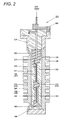
- FIG. 2 is a schematic cross-sectional view of the power module 300.
- the power module 300 houses a power semiconductor unit 330 (see FIG. 2 ), which includes a switching device and is transfer molded, in a metal module case 310.
- the power module 300 is used as a power converter mounted on an electric vehicle such as a pure electric car and a hybrid electric car.
- the module case 310 has a pair of heat sinks provided with a plurality of heat dissipation fins 305.
- the heat sinks are made of a metal such as aluminum having a high thermal conductivity.
- a heat sink located in the left side of the drawing has a thick portion 303 on which the heat dissipation fins 305 are erected and a thin portion 302 provided on the periphery thereof.
- the heat dissipation surface of the power semiconductor unit 330 housed inside and the inner peripheral surface of the thick portion 303 are in close contact by plastically deforming the thin portion 302. From one side of the module case 310, as shown in FIG. 1 , a DC positive electrode terminal 315B, a DC negative electrode terminal 319B, an AC terminal 321, and signal terminals 325L, 325U, 326L, and 326U provided in the power semiconductor unit 330 are protruded.
- FIG. 3 is an exploded perspective view of the power semiconductor unit 330
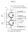
- FIG. 4 is a circuit diagram of the power semiconductor unit 330.
- a transfer mold is not shown in FIG. 3 .
- insulated-gate bipolar transistor (IGBT) chips 155 and 157 and diode chips 156 and 158 are provided as a power semiconductor device. While each two of the IGBT chips 155 and 157 and the diode chips 156 and 158 are disposed in parallel in the example shown in FIG. 3 , only one of them is shown in order to simplify the description in the circuit diagram of FIG. 4 .
- IGBT insulated-gate bipolar transistor
- a DC positive electrode lead frame 315 and a first AC electrode lead frame 316 are disposed in substantially the same plane on one side across the power semiconductor devices, and a second AC electrode lead frame 318 and a DC negative electrode lead frame 319 are disposed in substantially the same plane on the other side.
- the power semiconductor devices are flat plate-like structures and the front and back sides thereof are equipped with electrodes.
- the collector electrode of an upper arm IGBT chip 155 and the cathode electrode of an upper arm diode chip 156 are secured by solder 160.
- the collector electrode of a lower arm IGBT chip 157 and the cathode electrode of a lower arm diode chip 158 are secured by solder 160.
- the emitter electrode of the upper arm IGBT chip 155 and the anode electrode of the upper arm diode chip 156 are secured by solder 160.
- the emitter electrode of the lower arm IGBT chip 157 and the anode electrode of the lower arm diode chip 158 are secured by solder 160.
- the DC positive electrode lead frame 315 and the second AC electrode lead frame 318 are opposed substantially in parallel so as to sandwich the IGBT chips 155 and the diode chips 156.
- the first AC electrode lead frame 316 and the DC negative electrode lead frame 319 are opposed substantially in parallel so as to sandwich the IGBT chips 157 and the diode chips 158.
- the first AC electrode lead frame 316 and the second AC electrode lead frame 318 are connected via an intermediate electrode 159. Connection via the intermediate electrode 159 allows an upper arm circuit and a lower arm circuit to be connected, thereby forming a series circuit with the upper and lower arms as shown in FIG. 4 .
- a DC positive electrode wiring 315A is formed integrally with the DC positive electrode lead frame 315, and the distal end of the DC positive electrode wiring 315A is provided with the DC positive electrode terminal 315B.
- a DC negative electrode wiring 319A is formed integrally with the DC negative electrode lead frame 319, and the distal end of the DC negative electrode wiring 319A is provided with the DC negative electrode terminal 319B.
- An AC wiring 320 is formed integrally with the first AC electrode lead frame 316, and the end of the AC wiring 320 is provided with the AC terminal 321.
- a thermoplastic resin terminal block 600 is provided between the DC positive electrode wiring 315A and the DC negative electrode wiring 319A. As shown in FIG. 1 , the DC positive electrode wiring 315A and the DC negative electrode wiring 319A extend to protrude from the module case 310, being opposite and substantially parallel to each other.
- the signal terminals 325L, 325U, 326L, and 326U are integrally molded in the thermoplastic resin terminal block 600 and extend to protrude from the module case 310 in a direction similar to the DC positive electrode wiring 315A and the DC negative electrode wiring 319A. Accordingly, insulation between the DC positive electrode wiring 315A and the DC negative electrode wiring 319A and insulation between the signal wirings and wiring boards can be secured, and high-density wirings are possible.
- thermoplastic resin As a resin material used for the thermoplastic resin terminal block 600, a thermoplastic resin is suitable that has a heat resistance temperature equal to or higher than that of a mold of a transfer molding (e.g., 180°C or more) and insulation properties, so that polyphenylene sulfide (PPS), liquid crystal polymer (LCP), etc. are used.
- a transfer molding e.g. 180°C or more
- PPS polyphenylene sulfide
- LCP liquid crystal polymer
- FIG. 5 is a schematic cross-sectional view of the power semiconductor unit 330.
- FIG. 6 is a schematic diagram illustrating an electrode surface 11a of an emitter electrode 11 of an IGBT chip 1 and an electrode surface 21a of an anode electrode 21 of a diode chip 2, where FIG. 6 is an A-A cross-sectional view of FIG. 5 .
- a sealing member 20 and solders 5 and 7 are not illustrated. Note that, as shown in FIG. 6 , a direction in which the IGBT chip 1 and the diode chip 2 are aligned in a row is defined as the y direction, and a direction perpendicular to the y direction is defined as the x direction.
- upper arm components such as the upper arm IGBT chip, the upper arm diode chip, and various wirings for an upper arm and lower arm components such as the lower arm IGBT chip, the lower arm diode chip, and various wirings for a lower arm are almost the same configuration, the upper arm components and the lower arm components are defined and described as follows.
- the upper arm IGBT chip 155 and the lower arm IGBT chip 157 are merely referred to as the IGBT chip 1, and the upper arm diode chip 156 and the lower arm diode chip 158 are merely referred to as the diode chip 2.
- the second AC electrode lead frame 318 and the DC negative electrode lead frame 319 are merely referred to as a first bus bar 3, and the DC positive electrode lead frame 315 and the first AC electrode lead frame 316 are merely referred to as a second bus bar 4.
- Each of signal wirings including the signal terminals 325U, 325L, 326L, and 326U is referred to as a gate pin 9.
- one side of the IGBT chip 1 is provided with the electrode surface 11a of the emitter electrode 11 and terminal electrodes 13, i.e., an emitter terminal electrode 13a and a gate terminal electrode 13b, and the other side thereof is provided with an electrode surface 12a of a collector electrode 12.
- a drive signal from a driver circuit (not shown) connected to the power module is input to the gate terminal electrode 13b.
- Information of the current flowing through the emitter electrode 11 of the IGBT chip 1 is output from the emitter terminal electrode 13a.
- the IGBT chip 1 of the present embodiment is approximately the size of 10 mm x 10 mm.
- the electrode surface 11a of the emitter electrode 11 is connected to the first bus bar 3 with solder 5.
- the electrode surface 12a of the collector electrode 12 is connected to the second bus bar 4 with solder 6.
- the emitter terminal electrode 13a and the gate terminal electrode 13b are connected to the gate pin 9 by aluminum wire 10.
- One side of the diode chip 2 is provided with the electrode surface 21a of the anode electrode 21, and the other side thereof is provided with an electrode surface 22a of a cathode electrode 22.
- the electrode surface 21a of the anode electrode 21 is connected with solder 7 on the same plane as that of the first bus bar 3 where the IGBT chip 1 is connected.
- the electrode surface 22a of the cathode electrode 22 is connected with solder 8 on the same plane as that of the second bus bar 4 where the IGBT chip 1 is connected.
- An emitter electrode surface 11a, an anode electrode surface 21a, a collector electrode surface 12a, and a cathode electrode surface 22a are given surface processing, for example, such as nickel plating, that can be soldered.
- the first bus bar 3 and the second bus bar 4 are made of copper material, surface processing such as plating is not applied to the surface of the first bus bar 3 and the second bus bar 4 to be soldered, and the surface thereof is a solid copper material.
- the IGBT chip 1 and the diode chip 2 sandwiched between the first bus bar 3 and the second bus bar 4 and the aluminum wire 10 that connects the IGBT chip 1 and the gate pin 9 are sealed by the sealing member 20 made of an insulating organic material such as an epoxy resin having insulating properties.
- the other end of the connection portion of the gate pin 9 with the aluminum wire 10 protrudes outside of the sealing member 20, and is used as an external interface for the drive signal.
- the side opposite to the side on which the IGBT chip 1 (155, 157) and the diode chip 2 (156, 158) are connected in the first bus bar 3 (318, 319) and the second bus bar 4 (315, 316) is exposed without being sealed with a resin.
- the exposed side thereof is in contact with the inner surface of the module case 310 through an insulation sheet 333 and the like.
- heat generated from the IGBT chip 1 and the diode chip 2 is transmitted to the heat dissipation fins 305 of the module case 310 and the surface of the module case 310 through the first bus bar 3 (318, 319), the second bus bar 4 (315, 316), and the insulation sheet 333, and the heat is released from the refrigerant (not shown) in contact with the surfaces of the heat dissipation fins 305 and the module case 310.
- the electrode surface 11a of the emitter electrode 11 is double comb-shaped with four pairs of strip-shaped electrode surfaces protruding in the +y and -y directions from an electrode surface extending in the x direction in a plan view.
- the electrode surface 11a of the emitter electrode 11 has a primary solder spreading electrode surface 11a1 extending in the x direction in the center portion as illustrated and a secondary solder spreading electrode surface 11a2 extending in a comb-like manner from the primary solder spreading electrode surface 11a1 to both sides, i.e., in the +y and -y directions.
- the electrode surface 21a of the anode electrode 21 of the diode chip 2 is rectangular in a plan view as illustrated.
- the electrode surface 12a of the collector electrode 12 of the IGBT chip 1 and the electrode surface 22a of the cathode electrode 22 of the diode chip 2 are rectangular in a plan view.
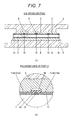
- FIG. 7(a) is a schematic cross-sectional view of the power semiconductor unit 330 taken along line B-B of FIG. 6
- FIG. 7(b) is an enlarged view of a part D of FIG. 7(a)
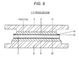
- FIG. 8 is a schematic cross-sectional view of the power semiconductor unit 330 taken along line C-C of FIG. 6
- the sealing member 20 is not shown in FIGS. 7 and 8 .
- an aluminum gate wiring 15 to connect a gate (not shown) and the gate terminal electrode 13b of each IGBT cell is provided between the strip-shaped electrode surfaces adjacent to each other that constitute the secondary solder spreading electrode surface 11a2.
- the aluminum gate wiring 15 and the gate of each IGBT cell are connected, for example, through a polysilicon wiring.
- the electrical resistance of the polysilicon wiring is tens to hundreds times higher than that of the aluminum gate wiring 15. Therefore a long polysilicon wiring increases electrical resistance to each IGBT cell, resulting in degradation of the response of each IGBT cell.
- the aluminum gate wiring 15 is provided on the periphery of the emitter electrode surface 11a including a space between the strip-shaped electrode surfaces adjacent to each other that constitute the secondary solder spreading electrode surface 11a2, and this shortens the polysilicon wiring.
- the aluminum gate wiring 15 is covered by a protective film 14 having insulating properties.
- a protective film is applied on the entire surface of the IGBT chip 1 including the electrode surfaces, and the protective film on the electrode surfaces is removed by etching after drying.
- the protective films 14 covering the aluminum gate wiring 15 are formed on the chip electrode surfaces.
- the periphery of the electrode surface 21a of the anode electrode 21 of the diode chip 2 is provided with a protective film 24 having insulating properties.
- a protective film 24 having insulating properties.
- polyimide resin and polyamide resin may be used as the protective films 14 and 24.
- the protective films 14 have low wettability to solder compared to the emitter electrode surface 11a of the IGBT chip 1. Accordingly, as shown in FIG. 7(b) , space where the solder 5 does not get wet and spread, i.e., a non-wetted space 16 where the solder 5 is not present, is formed on the protective films 14 formed between the strip-shaped electrode surfaces adjacent to each other that constitute the secondary solder spreading electrode surface 11a2 of the IGBT chip 1. Note that the non-wetted space 16 may communicate with the first bus bar 3 as shown by a broken line X in FIG. 7(a) .
- the protective film 14 does not exist on the C-C cross section of FIG. 6 , and the non-wetted space 16 does not exist except for soldering defects (not shown) such as voids (fine cavities).
- soldering defects not shown
- voids fine cavities
- FIG. 9 is a process diagram illustrating a manufacturing method of the power semiconductor unit 330
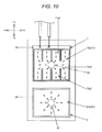
- FIG. 10 is a schematic view illustrating the setting positions of solders 5a and 7a and the spreading directions of the solders 5a and 7a.
- the IGBT chip 1 and the diode chip 2, the first bus bar 3, and the second bus bar 4 are first prepared, and molten solders 6a and 8a are dropped on solder dropping regions of the surface of the second bus bar 4 as shown in FIG. 9(a) .
- the solder dropping regions of the surface of the second bus bar 4 are a region facing the center position of the collector electrode surface 12a of the IGBT chip 1 and a region facing the center position of the cathode electrode surface 22a of the diode chip 2.
- the solder 6a is dropped on the solder dropping region of the second bus bar 4 facing the center position of the collector electrode surface 12a of the IGBT chip 1.
- the solder 8a is dropped on the solder dropping region of the second bus bar 4 facing the center position of the cathode electrode surface 22a of the diode chip 2.
- the IGBT chip 1 and the diode chip 2 are then positioned on the chip mounting surface of the second bus bar 4 such that the molten solder 6a is placed to face the center position of the collector electrode surface 12a of the IGBT chip 1 and the molten solder 8a is placed to face the center position of the cathode electrode surface 22a of the diode chip 2.
- the collector electrode surface 12a of the IGBT chip 1 and the cathode electrode surface 22a of the diode chip 2 are pressed against the molten solders 6a and 8a on the second bus bar 4 at the same time, and the molten solders 6a and 8a are spread on the collector electrode surface 12a and the cathode electrode surface 22a, respectively.
- a component thus formed is referred to as a second bus bar assembly 30.
- the collector electrode surface 12a of the IGBT chip 1 and the cathode electrode surface 22a of the diode chip 2 are rectangular in a plan view. Accordingly, the molten solders 6a and 8a placed at the centers of the corresponding electrode surfaces flow uniformly outward (radially) and spread over the corresponding entire electrode surfaces.
- molten solders 5a and 7a are dropped on dropping regions of the surface of the first bus bar 3.
- the dropping regions of the surface of the first bus bar 3 are a region facing a solder setting region 50 (see FIG. 10 ) located in the center of the emitter electrode surface 11a of the IGBT chip 1 and a region facing a solder setting region 70 (see FIG. 10 ) located in the center of the anode electrode surface 21a of the diode chip 2.
- the solder 5a is dropped on the dropping region of the first bus bar 3 facing the solder setting region 50
- the solder 7a is dropped on the dropping region of the first bus bar 3 facing the solder setting region 70a.
- the solder setting region 50 is set so as to include part of the primary solder spreading electrode surface 11a1 constituting the emitter electrode surface 11a of the IGBT chip 1.
- the second bus bar assembly 30 shown in FIG. 9(c) is turned over and the IGBT chip 1 and the diode chip 2 are positioned on the chip mounting surface of the first bus bar 3 such that the molten solder 5a is placed to face the solder setting region 50 (see FIG. 10 ) and the molten solder 7a is placed to face the solder setting region 70 (see FIG. 10 ).
- the emitter electrode surface 11a of the IGBT chip 1 and the anode electrode surface 21a of the diode chip 2 of the second bus bar assembly 30 turned over are pressed against the molten solders 5a and 7a on the first bus bar 3 at the same time.
- the molten solders 5a spreads outward (radially) from the solder setting region 50 of the emitter electrode surface 11a and the molten solders 7a spreads outward (radially) from the solder setting region 70 of the anode electrode surface 21a, as shown schematically by arrows in FIG. 10 .
- the anode electrode surface 21a of the diode chip 2 is rectangular in a plan view. Accordingly, the molten solders 7a flows uniformly outward (radially) from the solder setting region 70 in the center of the anode electrode surface 21a and spreads over the entire anode electrode surface 21a.
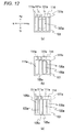
- FIG. 11 is a schematic view illustrating a state where the molten solder 5a spreads on the emitter electrode surface 11a of the IGBT chip 1.
- the molten solder 5a flows from the center of the primary solder spreading electrode surface 11a1 in the +x and -x directions as shown in FIGS. 11 (a) to 11 (c) .
- the solder 5a advances from the primary solder spreading electrode surface 11a1 to the secondary solder spreading electrode surface 11a2 and flows toward the end of the secondary solder spreading electrode surface 11a2, i.e., in the +y and -y directions, at which time the molten solder 5a does not spread in the direction across the protective film 14.
- the wettability of the solder of the protective film 14 provided on the periphery of the double comb-shaped emitter electrode surface 11a including a space between the strip-shaped electrode surfaces adjacent to each other that constitute the secondary solder spreading electrode surface 11a2 is low compared to the emitter electrode surface 11a.
- the wettability of the emitter electrode surface 11a to the solder is good compared to the wettability of the protective film 14 to the solder.
- the molten solder 5a spreads from the primary solder spreading electrode surface 11a1 to the secondary solder spreading electrode surface 11a2 along the double comb-shaped emitter electrode 11 (see FIGS. 11(a) and 11(b) ), and finally spreads over the emitter electrode surface 11a (see FIG. 11(c) ).
- solder 5a also can be uniformly spread on the emitter electrode surface 11a, and this may achieve reduction of solder 5a protrusion and the effect of reducing voids.
- the first bus bar 3 is connected to the emitter electrode surface 11a of the IGBT chip 1 by the solder 5 and the first bus bar 3 is connected to the anode electrode surface 21a of the diode chip 2 by the solder 7, as shown in FIG. 9(f) .
- each of the electrode surfaces of the terminal electrodes 13 (13a, 13b) of the IGBT chip 1 and the gate pin 9 are electrically connected by the aluminum wire 10, members including the first bus bar 3 and the second bus bar 4 are sealed by the sealing member 20, and thus the power semiconductor unit 330 is completed (see FIG. 5 ).
- FIG. 12 is a schematic view illustrating a state where molten solder 105a spreads on emitter electrode surfaces 111a of a conventional IGBT chip 101.
- the conventional IGBT chip 101 is provided with a plurality of strip-shaped emitter electrode surfaces 111a. Note that the wettability of a protective film 114 interposed between adjacent strip-shaped emitter electrode surfaces 111a to the solder 105a is low compared to the wettability of the emitter electrode surface 111a to the solder 105a.
- the solder 105a does not spread over the entire emitter electrode surfaces 111a, so that a non-solder-wetting area 105b where the solder 105a is not present on the emitter electrode surface 111a may be formed, and the solder 105a may flow beyond the emitter electrode surface 111a to cause a solder flow 105c.
- JP 2006-210519 A discloses a technique to improve the connection with the solder by providing a polyimide film (insulating protective film) with a metal foil.
- This conventional technique can uniformly spread the solder on a chip.
- the conventional technique where the polyimide film is provided with the metal foil, is expensive.
- new junctions of the metal foil and the solder as well as the polyimide film and the metal foil may reduce the life of the joint.
- An electrode surface 611a shown in FIG. 15(a) has a primary solder spreading electrode surface 611a1 extending in the x direction, a secondary solder spreading electrode surface 611a2 extending in a comb-like manner in the +y direction from the primary solder spreading electrode surface 611a1, and a secondary solder spreading electrode surface 611a3 extending in a comb-like manner in the -y direction from the primary solder spreading electrode surface 611a1.
- the secondary solder spreading electrode surface 611a2 extending in the +y direction has four strip-shaped electrode surfaces, while the secondary solder spreading electrode surface 611a3 extending in the -y direction has three strip-shaped electrode surfaces.
- a electrode surface 711a shown in FIG. 15(b) has a primary solder spreading electrode surface 711a1 extending in the x direction, a secondary solder spreading electrode surface 711a2 extending in a comb-like manner in the +y direction from the primary solder spreading electrode surface 711a1, and a secondary solder spreading electrode surface 711a3 extending in a comb-like manner in the -y direction from the primary solder spreading electrode surface 711a1.
- the secondary solder spreading electrode surface 711a2 extending in the +y direction has four strip-shaped electrode surfaces, while the secondary solder spreading electrode surface 711a3 extending in the -y direction has six strip-shaped electrode surfaces.
- the width in the x direction of each of the strip-shaped electrode surfaces of the secondary solder spreading electrode surface 711a2 is different from that of each of the strip-shaped electrode surfaces of the secondary solder spreading electrode surface 711a3.
- An electrode surface 811a shown in FIG. 15(c) has three pairs of narrow strip-shaped electrode surfaces and two pairs of wide strip-shaped electrode surfaces, these electrode surfaces extending from a primary solder spreading electrode surface 811a1 to both sides (in the +y and -y directions).
- the primary solder spreading electrode surface extending in one direction and the secondary solder spreading electrode surface extending in a comb-like manner from the primary solder spreading electrode surface to both sides thereof allows the solder placed at a solder setting region including the primary solder spreading electrode surface to spread over the entire electrode surfaces.
- the manufacturing method of the power semiconductor unit 330 according to the present invention is not limited to that shown in FIG. 9 .
- the following method may be employed that includes: dropping the molten solders 6a and 8a on the IGBT chip 1 and the diode chip 2, pressing the second bus bar 4 against the molten solders 6a and 8a from above, with the IGBT chip 1 and the diode chip 2 being disposed downward, connecting the second bus bar 4 and the IGBT chip 1 and the diode chip 2 with the solder 6 and 8 to form the second bus bar assembly 30, turning over and placing the second bus bar assembly 30 thereafter, dropping the molten solders 5a and 7a on the IGBT chip 1 and the diode chip 2, pressing the first bus bar 3 against the molten solders 5a and 7a from above, with the second bus bar assembly 30 being disposed downward, and connecting the first bus bar 3 and the IGBT chip 1 and the diode chip 2 are connected with solder 5 and 7.
- the present invention is not necessarily limited to the case where the IGBT chip 1 and the diode chip 2 are simultaneously moved toward the second bus bar 4 and are joined together.
- the connection of the second bus bar 4 and the IGBT chip 1 and the diode chip 2 and the connection of the first bus bar 3 and the IGBT chip 1 and the diode chip 2 may be performed in reverse order.
- a dropping method is employed whereby molten solder is dropped and electrode surfaces of a semiconductor device and a bus bar are connected with solder
- the present invention is not limited thereto.
- a method may be employed whereby cream solder is placed at a solder setting region, then enters, for example, a heating furnace, and is caused to reflow.
- a semiconductor device having at least one double comb-shaped electrode surface on one side thereof, a first conductive member, and a second conductive member are prepared.
- an electrode surface provided on the other side of the semiconductor device is connected to the second conductive member with solder.
- the cream solder is placed at a predetermined region including part of a primary solder spreading electrode surface constituting a double comb-shaped electrode surface of the semiconductor device, for example, at the solder setting region 50 of FIG. 10 or at a region of the first conductive member facing the predetermined region.
- the cream solder is melted by heating, the molten solder is spread from the primary solder spreading electrode surface to a secondary solder spreading electrode surface by reducing a distance between the first conductive member and the electrode surface provided on the one side of the semiconductor device, and the electrode surface provided on the one side of the semiconductor device is connected to the first conductive member with solder.
- the first and second conductive members are sealed with a sealing member.
- the cream solder is set at the predetermined region, the cream solder is molten by heating, the conductive members and the electrode surfaces of the semiconductor device are moved closer to each other, and thus the molten solder can be spread over the electrode surfaces.
- an IGBT is employed as a switching semiconductor device in the embodiments described above, other semiconductor devices, for example, such as a metal-oxide-semiconductor field-effect transistor (MOSFET) may be employed depending on the required voltage and frequency.
- MOSFET metal-oxide-semiconductor field-effect transistor
- the IGBT is suitable for relatively high DC voltage
- the MOSFET is suitable for relatively low DC voltage.
- the electrode surface of the emitter electrode is double comb-shaped in the embodiments described above, the present invention is not limited thereto. At least one of the electrode surfaces provided on the one side of the semiconductor device only needs to be double comb-shaped.
- the present invention is not limited thereto.
- the present invention may be applicable to power modules mounted on power converters available to power supplies for other vehicles, for example, railway vehicles such as a hybrid electric train, vehicles carrying passengers such as a bus, vehicles used to carry goods such as a truck, and industrial vehicles such as a battery-powered forklift truck.
Landscapes
- Inverter Devices (AREA)
- Cooling Or The Like Of Semiconductors Or Solid State Devices (AREA)
- Electrodes Of Semiconductors (AREA)
- Chemical & Material Sciences (AREA)
- Engineering & Computer Science (AREA)
- Materials Engineering (AREA)
Abstract
Description
- The present invention relates to a power module configured so that both sides of a semiconductor device are connected to conductive members with solder.
- A power semiconductor device such as an IGBT chip is used as a power module mounted, for example, on a power converter for a hybrid electric car and a pure electric car. The IGBT chip has a structure where several thousands to several tens of thousands of IGBT cells are repeatedly arranged. The IGBT chip is a three-terminal device having an emitter electrode, a collector electrode, and a gate electrode, in the structure of which the emitter electrode and the gate electrode are formed in an insulated state on the same plane of the IGBT chip.
- In order to reduce the variation of the propagation delay time of a control signal, the gate electrode is connected to a gate wiring made of a material having a high conductivity such as aluminum, and the gate wiring is connected to a gate of the IGBT cell, for example, through a polysilicon wiring.
- The emitter electrode of the IGBT chip is generally divided into multiple regions by the gate wiring (see PTL 1).
The emitter electrode divided may be connected to a conductive member with solder. - In the power module mounted, for example, on a power converter for a hybrid electric car and a pure electric car, the input current tends to be increased as systems in recent years are powered up. When solder is used to connect a semiconductor device and a conductive member, an increase in the input current increases the temperature change of the semiconductor device, resulting in the degradation of the solder connecting the semiconductor device and the conductive member. Since the degradation of the solder affects the void fraction, suppression of voids that occur during soldering is an important issue in improving the life of the solder to a temperature change.
- PTL 1:
JP 2004-221269A - In a common type of power module, such as described in
PTL 1, an emitter electrode is divided into multiple regions by aluminum gate wiring having a small electric resistance compared to polysilicon wiring. The aluminum gate wiring is covered with a protective film having insulating properties, such as polyimide resin having low wettability to solder. - Thus, when an emitter electrode surface and a conductive member are connected with the solder, spreading of the solder on the emitter electrode surface of an IGBT chip is limited by the protective film and the solder flows unevenly, and this leads to a problem that the void fraction becomes high. In addition, since the spreading direction of the solder is limited to a predetermined direction, the solder flows too much in that direction, and the solder may flow beyond the emitter electrode surface of the IGBT chip.
- A power module according to a first aspect of the invention includes: a semiconductor device having at least one electrode surface on each side thereof; a first conductive member connected to the electrode surface provided on one side of the semiconductor device with solder; and a second conductive member connected to the electrode surface provided on the other side of the semiconductor device with solder, with at least one of the electrode surfaces provided on the one side of the semiconductor device being double comb-shaped.
- According to a second aspect of the invention, which is the power module of the first aspect, the double comb-shaped electrode surface preferably has a primary solder spreading electrode surface and a secondary solder spreading electrode surface extending in a comb-like manner from the primary solder spreading electrode surface to both sides thereof.
- According to a third aspect of the invention, which is the first or second power module, preferably the periphery of the double comb-shaped electrode surface is provided with a gate wiring, and the gate wiring is covered with a protective film having low wettability to solder compared to the double comb-shaped electrode surface and insulating properties.
- According to a fourth aspect of the invention, which is the power module of any one of the first to third aspects, preferably the first and second conductive members are made of copper material, and no surface treatment is applied to the surface of the first and second conductive members to be soldered.
- A power module according to a fifth aspect of the invention includes: an IGBT chip and a diode chip; a first conductive plate that is connected with solder to an emitter electrode surface provided on one side of the IGBT chip and to an anode electrode surface provided on one side of the diode chip; and a second conductive plate that is connected with solder to a collector electrode surface provided on the other side of the IGBT chip and to a cathode electrode surface provided on the other side of the diode chip. At least one of the emitter electrode surfaces provided on the one side of the IGBT chip is double comb-shaped, the double comb-shaped electrode surface has a primary solder spreading electrode surface and a secondary solder spreading electrode surface extending in a comb-like manner from the primary solder spreading electrode surface to both sides thereof, the periphery of the emitter electrode surface is provided with a gate wiring, and the gate wiring is covered with a protective film having low wettability to solder compared to the emitter electrode surface and insulating properties.
- A power module according to a sixth aspect of the invention includes: an upper arm IGBT chip and an upper arm diode chip and a lower arm IGBT chip and a lower arm diode chip that make up an upper arm and a lower arm of an inverter circuit; a second AC electrode lead frame that is connected with solder to at least one emitter electrode surface provided on one side of the upper arm IGBT chip and to an anode electrode surface provided on one side of the upper arm diode chip; a DC positive electrode lead frame that is connected with solder to a collector electrode surface provided on the other side of the upper arm IGBT chip and to a cathode electrode surface provided on the other side of the upper arm diode chip; a DC negative electrode lead frame that is connected with solder to at least one emitter electrode surface provided on one side of the lower arm IGBT chip and to an anode electrode surface provided on one side of the lower arm diode chip; and a first AC electrode lead frame that is connected with solder to a collector electrode surface provided on the other side of the lower arm IGBT chip and to a cathode electrode surface provided on the other side of the lower arm diode chip. At least one of the emitter electrode surfaces provided on each of the one sides of the upper arm IGBT chip and the lower arm IGBT chip is double comb-shaped, the double comb-shaped electrode surface has a primary solder spreading electrode surface and a secondary solder spreading electrode surface extending in a comb-like manner from the primary solder spreading electrode surface to both sides thereof, the periphery of the emitter electrode surface is provided with a gate wiring, and the gate wiring is covered with a protective film having low wettability to solder compared to the emitter electrode surface and insulating properties.
- According to a seventh aspect of the invention, which is the power module of any one of the first to sixth aspects, nickel plating to improve the wettability to solder is preferably applied to the double comb-shaped electrode surface.
- A method of manufacturing a power module according to an eighth aspect of the invention, which is a method of manufacturing the power module of any one of the second to fourth aspects, includes: preparing the semiconductor device having at least one double comb-shaped electrode surface, the first conductive member, and the second conductive member; connecting the electrode surface provided on the other side of the semiconductor device to the second conductive member with solder; dropping molten solder on a predetermined region including part of the primary solder spreading electrode surface constituting the double comb-shaped electrode surface of the semiconductor device or on a region of the first conductive member facing the predetermined region; spreading the molten solder from the primary solder spreading electrode surface to the secondary solder spreading electrode surface by reducing a distance between the first conductive member and the electrode surface provided on the one side of the semiconductor device and connecting the electrode surface provided on the one side of the semiconductor device to the first conductive member with solder; and sealing the first and second conductive members with a sealing member.
- A method of manufacturing a power module according to an ninth aspect of the invention, which is a method of manufacturing the power module of any one of the second to fourth aspects, includes: preparing the semiconductor device having at least one double comb-shaped electrode surface, the first conductive member, and the second conductive member; connecting the electrode surface provided on the other side of the semiconductor device to the second conductive member with solder; dropping molten solder on a dropping region of the first conductive member; performing positioning such that the solder dropped on the dropping region is disposed so as to face a predetermined region including part of the primary solder spreading electrode surface constituting the double comb-shaped electrode surface provided on the one side of the semiconductor device; moving the one side of the semiconductor device toward the first conductive member, spreading the molten solder from the primary solder spreading electrode surface to the secondary solder spreading electrode surface, and connecting the electrode surface provided on the one surface of the semiconductor device to the first conductive member with solder; and sealing the first and second conductive members with a sealing member.
- A method of manufacturing a power module according to an tenth aspect of the invention, which is a method of manufacturing the power module of the fifth aspect, includes: preparing the IGBT chip having at least one double comb-shaped emitter electrode surface, the diode chip, the first conductive plate, and the second conductive plate; dropping molten solder at the center positions of the collector electrode surface of the IGBT chip and the cathode electrode surface of the diode chip or at predetermined positions of the second conductive plate facing the center positions thereof; simultaneously moving the collector electrode surface of the IGBT chip and the cathode electrode surface of the diode chip toward the second conductive plate, spreading the molten solder on the collector electrode surface and the cathode electrode surface, and connecting the collector electrode surface of the IGBT chip and the cathode electrode surface of the diode chip to the second conductive plate with solder; dropping molten solder at a predetermined region including part of the primary solder spreading electrode surface constituting the emitter electrode surface of the IGBT chip and at the center position of the anode electrode surface of the diode chip or at predetermined positions of the first conductive plate facing the predetermined region and the center position of the anode electrode surface; simultaneously moving the emitter electrode surface of the IGBT chip and the anode electrode surface of the diode chip toward the first conductive plate, spreading the molten solder from the primary solder spreading electrode surface to the secondary solder spreading electrode surface of the emitter electrode surface and spreading the molten solder on the anode electrode surface, and connecting the emitter electrode surface of the IGBT chip and the anode electrode surface of the diode chip to the first conductive plate with solder; and sealing the first and second conductive plates with a sealing member.
- A method of manufacturing a power module according to an eleventh aspect of the invention, which is a method of manufacturing the power module of any one of the second to fourth aspects, includes: preparing the semiconductor device having at least one double comb-shaped electrode surface, the first conductive member, and the second conductive member; connecting the electrode surface provided on the other side of the semiconductor device to the second conductive member with solder; placing solder at a predetermined region including part of the primary solder spreading electrode surface constituting the double comb-shaped electrode surface of the semiconductor device or at a region of the first conductive member facing the predetermined region; melting the solder by heating, spreading the molten solder from the primary solder spreading electrode surface to the secondary solder spreading electrode surface by reducing a distance between the first conductive member and the electrode surface provided on the one side of the semiconductor device, and connecting the electrode surface provided on the one side of the semiconductor device to the first conductive member with solder; and sealing the first and second conductive members with a sealing member.
- The present invention suppresses the occurrence of voids and controls solder flow, and can prolong the life of a solder joint, thereby providing a power module with a high reliability and a manufacturing method thereof.
-
- [
FIG. 1] FIG. 1 is a perspective view showing the appearance of a power module. - [
FIG. 2] FIG. 2 is a schematic cross-sectional view of the power module. - [
FIG. 3] FIG. 3 is an exploded perspective view of a power semiconductor unit. - [
FIG. 4] FIG. 4 is a circuit diagram of the power semiconductor unit. - [
FIG. 5] FIG. 5 is a schematic cross-sectional view of the power semiconductor unit. - [
FIG. 6] FIG. 6 is a schematic diagram illustrating an emitter electrode surface of an IGBT chip and an anode electrode surface of a diode chip. - [
FIG. 7] FIG. 7(a) is a schematic cross-sectional view of the power semiconductor unit taken along line B-B ofFIG. 6 , andFIG. 7(b) is an enlarged view of a part D ofFIG. 7(a) . - [
FIG. 8] FIG. 8 is a schematic cross-sectional view of the power semiconductor unit taken along line C-C ofFIG. 6 . - [
FIG. 9] FIG. 9 is a process diagram illustrating a manufacturing method of the power semiconductor unit. - [
FIG. 10] FIG. 10 is a schematic view illustrating the setting position of solder and the spreading directions of solder. - [
FIG. 11] FIG. 11 is a schematic view illustrating a state where molten solder spreads on the emitter electrode surface of the IGBT chip. - [
FIG. 12] FIG. 12 is a schematic view illustrating a state where molten solder spreads on the emitter electrode surfaces of a conventional IGBT chip. - [
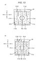
FIG. 13] FIG. 13 is a schematic view illustrating the setting position of solder and the spreading directions of solder on the emitter electrode surface of an IGBT chip according to a modification. - [
FIG. 14] FIG. 14 is a schematic view illustrating the setting position of solder and the spreading directions of solder on the emitter electrode surface of an IGBT chip according to a modification. - [
FIG. 15] FIG. 15 is a schematic view illustrating the emitter electrode surface of an IGBT chip according to a modification. - Embodiments of the present invention will now be described with reference to the drawings.
FIG. 1 is a perspective view showing the appearance of apower module 300, andFIG. 2 is a schematic cross-sectional view of thepower module 300. Thepower module 300 houses a power semiconductor unit 330 (seeFIG. 2 ), which includes a switching device and is transfer molded, in ametal module case 310. Thepower module 300 is used as a power converter mounted on an electric vehicle such as a pure electric car and a hybrid electric car. - The
module case 310 has a pair of heat sinks provided with a plurality ofheat dissipation fins 305. The heat sinks are made of a metal such as aluminum having a high thermal conductivity. As shown inFIG. 2 , a heat sink located in the left side of the drawing has athick portion 303 on which theheat dissipation fins 305 are erected and athin portion 302 provided on the periphery thereof. The heat dissipation surface of thepower semiconductor unit 330 housed inside and the inner peripheral surface of thethick portion 303 are in close contact by plastically deforming thethin portion 302. From one side of themodule case 310, as shown inFIG. 1 , a DCpositive electrode terminal 315B, a DCnegative electrode terminal 319B, anAC terminal 321, andsignal terminals power semiconductor unit 330 are protruded. -
FIG. 3 is an exploded perspective view of thepower semiconductor unit 330, andFIG. 4 is a circuit diagram of thepower semiconductor unit 330. A transfer mold is not shown inFIG. 3 . In the present embodiment, insulated-gate bipolar transistor (IGBT)chips diode chips IGBT chips diode chips FIG. 3 , only one of them is shown in order to simplify the description in the circuit diagram ofFIG. 4 . - As shown in
FIG. 3 , a DC positiveelectrode lead frame 315 and a first ACelectrode lead frame 316 are disposed in substantially the same plane on one side across the power semiconductor devices, and a second ACelectrode lead frame 318 and a DC negativeelectrode lead frame 319 are disposed in substantially the same plane on the other side. - The power semiconductor devices are flat plate-like structures and the front and back sides thereof are equipped with electrodes. On a
device securing region 322 of the DC positiveelectrode lead frame 315, the collector electrode of an upperarm IGBT chip 155 and the cathode electrode of an upperarm diode chip 156 are secured bysolder 160. - On the other hand, on the
device securing region 322 of the first ACelectrode lead frame 316, the collector electrode of a lowerarm IGBT chip 157 and the cathode electrode of a lowerarm diode chip 158 are secured bysolder 160. - On the
device securing region 322 of the second ACelectrode lead frame 318, the emitter electrode of the upperarm IGBT chip 155 and the anode electrode of the upperarm diode chip 156 are secured bysolder 160. On the other hand, on thedevice securing region 322 of the DC negativeelectrode lead frame 319, the emitter electrode of the lowerarm IGBT chip 157 and the anode electrode of the lowerarm diode chip 158 are secured bysolder 160. - As shown in
FIG. 3 , the DC positiveelectrode lead frame 315 and the second ACelectrode lead frame 318 are opposed substantially in parallel so as to sandwich the IGBT chips 155 and the diode chips 156. Likewise, the first ACelectrode lead frame 316 and the DC negativeelectrode lead frame 319 are opposed substantially in parallel so as to sandwich the IGBT chips 157 and the diode chips 158. As shown inFIG. 4 , the first ACelectrode lead frame 316 and the second ACelectrode lead frame 318 are connected via anintermediate electrode 159. Connection via theintermediate electrode 159 allows an upper arm circuit and a lower arm circuit to be connected, thereby forming a series circuit with the upper and lower arms as shown inFIG. 4 . - As shown in
FIG. 3 , a DCpositive electrode wiring 315A is formed integrally with the DC positiveelectrode lead frame 315, and the distal end of the DCpositive electrode wiring 315A is provided with the DCpositive electrode terminal 315B. Likewise, a DCnegative electrode wiring 319A is formed integrally with the DC negativeelectrode lead frame 319, and the distal end of the DCnegative electrode wiring 319A is provided with the DCnegative electrode terminal 319B. AnAC wiring 320 is formed integrally with the first ACelectrode lead frame 316, and the end of theAC wiring 320 is provided with theAC terminal 321. - A thermoplastic
resin terminal block 600 is provided between the DCpositive electrode wiring 315A and the DCnegative electrode wiring 319A. As shown inFIG. 1 , the DCpositive electrode wiring 315A and the DCnegative electrode wiring 319A extend to protrude from themodule case 310, being opposite and substantially parallel to each other. Thesignal terminals resin terminal block 600 and extend to protrude from themodule case 310 in a direction similar to the DCpositive electrode wiring 315A and the DCnegative electrode wiring 319A. Accordingly, insulation between the DCpositive electrode wiring 315A and the DCnegative electrode wiring 319A and insulation between the signal wirings and wiring boards can be secured, and high-density wirings are possible. - As a resin material used for the thermoplastic
resin terminal block 600, a thermoplastic resin is suitable that has a heat resistance temperature equal to or higher than that of a mold of a transfer molding (e.g., 180°C or more) and insulation properties, so that polyphenylene sulfide (PPS), liquid crystal polymer (LCP), etc. are used. -
FIG. 5 is a schematic cross-sectional view of thepower semiconductor unit 330.FIG. 6 is a schematic diagram illustrating anelectrode surface 11a of anemitter electrode 11 of anIGBT chip 1 and anelectrode surface 21a of ananode electrode 21 of adiode chip 2, whereFIG. 6 is an A-A cross-sectional view ofFIG. 5 . InFIG. 6 , a sealingmember 20 andsolders FIG. 6 , a direction in which theIGBT chip 1 and thediode chip 2 are aligned in a row is defined as the y direction, and a direction perpendicular to the y direction is defined as the x direction. - Since upper arm components such as the upper arm IGBT chip, the upper arm diode chip, and various wirings for an upper arm and lower arm components such as the lower arm IGBT chip, the lower arm diode chip, and various wirings for a lower arm are almost the same configuration, the upper arm components and the lower arm components are defined and described as follows.
- The upper
arm IGBT chip 155 and the lowerarm IGBT chip 157 are merely referred to as theIGBT chip 1, and the upperarm diode chip 156 and the lowerarm diode chip 158 are merely referred to as thediode chip 2. The second ACelectrode lead frame 318 and the DC negativeelectrode lead frame 319 are merely referred to as afirst bus bar 3, and the DC positiveelectrode lead frame 315 and the first ACelectrode lead frame 316 are merely referred to as asecond bus bar 4. Each of signal wirings including thesignal terminals gate pin 9. - As shown in
FIGS. 5 and6 , one side of theIGBT chip 1 is provided with theelectrode surface 11a of theemitter electrode 11 andterminal electrodes 13, i.e., anemitter terminal electrode 13a and agate terminal electrode 13b, and the other side thereof is provided with anelectrode surface 12a of acollector electrode 12. A drive signal from a driver circuit (not shown) connected to the power module is input to thegate terminal electrode 13b. Information of the current flowing through theemitter electrode 11 of theIGBT chip 1 is output from theemitter terminal electrode 13a. TheIGBT chip 1 of the present embodiment is approximately the size of 10 mm x 10 mm. - The
electrode surface 11a of theemitter electrode 11 is connected to thefirst bus bar 3 withsolder 5. Theelectrode surface 12a of thecollector electrode 12 is connected to thesecond bus bar 4 withsolder 6. Theemitter terminal electrode 13a and thegate terminal electrode 13b are connected to thegate pin 9 byaluminum wire 10. - One side of the
diode chip 2 is provided with theelectrode surface 21a of theanode electrode 21, and the other side thereof is provided with anelectrode surface 22a of acathode electrode 22. Theelectrode surface 21a of theanode electrode 21 is connected withsolder 7 on the same plane as that of thefirst bus bar 3 where theIGBT chip 1 is connected. Theelectrode surface 22a of thecathode electrode 22 is connected withsolder 8 on the same plane as that of thesecond bus bar 4 where theIGBT chip 1 is connected. - An
emitter electrode surface 11a, ananode electrode surface 21a, acollector electrode surface 12a, and acathode electrode surface 22a are given surface processing, for example, such as nickel plating, that can be soldered. On the other hand, thefirst bus bar 3 and thesecond bus bar 4 are made of copper material, surface processing such as plating is not applied to the surface of thefirst bus bar 3 and thesecond bus bar 4 to be soldered, and the surface thereof is a solid copper material. - As shown in
FIG. 5 , theIGBT chip 1 and thediode chip 2 sandwiched between thefirst bus bar 3 and thesecond bus bar 4 and thealuminum wire 10 that connects theIGBT chip 1 and thegate pin 9 are sealed by the sealingmember 20 made of an insulating organic material such as an epoxy resin having insulating properties. The other end of the connection portion of thegate pin 9 with thealuminum wire 10 protrudes outside of the sealingmember 20, and is used as an external interface for the drive signal. - As shown in
FIG. 2 , the side opposite to the side on which the IGBT chip 1 (155, 157) and the diode chip 2 (156, 158) are connected in the first bus bar 3 (318, 319) and the second bus bar 4 (315, 316) is exposed without being sealed with a resin. The exposed side thereof is in contact with the inner surface of themodule case 310 through aninsulation sheet 333 and the like. Accordingly, heat generated from theIGBT chip 1 and thediode chip 2 is transmitted to theheat dissipation fins 305 of themodule case 310 and the surface of themodule case 310 through the first bus bar 3 (318, 319), the second bus bar 4 (315, 316), and theinsulation sheet 333, and the heat is released from the refrigerant (not shown) in contact with the surfaces of theheat dissipation fins 305 and themodule case 310. - As shown in
FIG. 6 , theelectrode surface 11a of theemitter electrode 11 is double comb-shaped with four pairs of strip-shaped electrode surfaces protruding in the +y and -y directions from an electrode surface extending in the x direction in a plan view. Specifically, theelectrode surface 11a of theemitter electrode 11 has a primary solder spreading electrode surface 11a1 extending in the x direction in the center portion as illustrated and a secondary solder spreading electrode surface 11a2 extending in a comb-like manner from the primary solder spreading electrode surface 11a1 to both sides, i.e., in the +y and -y directions. - The
electrode surface 21a of theanode electrode 21 of thediode chip 2 is rectangular in a plan view as illustrated. Although not illustrated, theelectrode surface 12a of thecollector electrode 12 of theIGBT chip 1 and theelectrode surface 22a of thecathode electrode 22 of thediode chip 2 are rectangular in a plan view. -
FIG. 7(a) is a schematic cross-sectional view of thepower semiconductor unit 330 taken along line B-B ofFIG. 6 , andFIG. 7(b) is an enlarged view of a part D ofFIG. 7(a) .FIG. 8 is a schematic cross-sectional view of thepower semiconductor unit 330 taken along line C-C ofFIG. 6 . The sealingmember 20 is not shown inFIGS. 7 and8 . As shown inFIGS. 6 and7 , analuminum gate wiring 15 to connect a gate (not shown) and thegate terminal electrode 13b of each IGBT cell is provided between the strip-shaped electrode surfaces adjacent to each other that constitute the secondary solder spreading electrode surface 11a2. - Although not shown, the
aluminum gate wiring 15 and the gate of each IGBT cell are connected, for example, through a polysilicon wiring. The electrical resistance of the polysilicon wiring is tens to hundreds times higher than that of thealuminum gate wiring 15. Therefore a long polysilicon wiring increases electrical resistance to each IGBT cell, resulting in degradation of the response of each IGBT cell. In the present embodiment, thealuminum gate wiring 15 is provided on the periphery of theemitter electrode surface 11a including a space between the strip-shaped electrode surfaces adjacent to each other that constitute the secondary solder spreading electrode surface 11a2, and this shortens the polysilicon wiring. - As shown in
FIGS. 6 to 8 , thealuminum gate wiring 15 is covered by aprotective film 14 having insulating properties. A protective film is applied on the entire surface of theIGBT chip 1 including the electrode surfaces, and the protective film on the electrode surfaces is removed by etching after drying. Thus, as shown inFIGS. 7 and8 , theprotective films 14 covering thealuminum gate wiring 15 are formed on the chip electrode surfaces. As shown inFIG. 6 , the periphery of theelectrode surface 21a of theanode electrode 21 of thediode chip 2 is provided with aprotective film 24 having insulating properties. For example, polyimide resin and polyamide resin may be used as theprotective films - The
protective films 14 have low wettability to solder compared to theemitter electrode surface 11a of theIGBT chip 1. Accordingly, as shown inFIG. 7(b) , space where thesolder 5 does not get wet and spread, i.e., anon-wetted space 16 where thesolder 5 is not present, is formed on theprotective films 14 formed between the strip-shaped electrode surfaces adjacent to each other that constitute the secondary solder spreading electrode surface 11a2 of theIGBT chip 1. Note that thenon-wetted space 16 may communicate with thefirst bus bar 3 as shown by a broken line X inFIG. 7(a) . - As shown in
FIG. 8 , theprotective film 14 does not exist on the C-C cross section ofFIG. 6 , and thenon-wetted space 16 does not exist except for soldering defects (not shown) such as voids (fine cavities). Thus, thenon-wetted space 16 exists on theprotective film 14 formed between the strip-shaped electrode surfaces adjacent to each other that constitute the secondary solder spreading electrode surface 11a2 (seeFIG. 7 ). - An embodiment of a manufacturing method of the power module according to the present invention is described with reference to
FIGS. 9 and10 .FIG. 9 is a process diagram illustrating a manufacturing method of thepower semiconductor unit 330, andFIG. 10 is a schematic view illustrating the setting positions ofsolders solders - The
IGBT chip 1 and thediode chip 2, thefirst bus bar 3, and thesecond bus bar 4 are first prepared, andmolten solders second bus bar 4 as shown inFIG. 9(a) . The solder dropping regions of the surface of thesecond bus bar 4 are a region facing the center position of thecollector electrode surface 12a of theIGBT chip 1 and a region facing the center position of thecathode electrode surface 22a of thediode chip 2. Thesolder 6a is dropped on the solder dropping region of thesecond bus bar 4 facing the center position of thecollector electrode surface 12a of theIGBT chip 1. Thesolder 8a is dropped on the solder dropping region of thesecond bus bar 4 facing the center position of thecathode electrode surface 22a of thediode chip 2. - As shown in
FIG. 9(b) , theIGBT chip 1 and thediode chip 2 are then positioned on the chip mounting surface of thesecond bus bar 4 such that themolten solder 6a is placed to face the center position of thecollector electrode surface 12a of theIGBT chip 1 and themolten solder 8a is placed to face the center position of thecathode electrode surface 22a of thediode chip 2. - After positioning, the
collector electrode surface 12a of theIGBT chip 1 and thecathode electrode surface 22a of thediode chip 2 are pressed against themolten solders second bus bar 4 at the same time, and themolten solders collector electrode surface 12a and thecathode electrode surface 22a, respectively. This allows thecollector electrode surface 12a of theIGBT chip 1 and thecathode electrode surface 22a of thediode chip 2 to be connected together to thesecond bus bar 4 with thesolder FIG. 9(c) . - A component thus formed is referred to as a second
bus bar assembly 30. As noted above, thecollector electrode surface 12a of theIGBT chip 1 and thecathode electrode surface 22a of thediode chip 2 are rectangular in a plan view. Accordingly, themolten solders - As shown in
FIG. 9(d) ,molten solders first bus bar 3. The dropping regions of the surface of thefirst bus bar 3 are a region facing a solder setting region 50 (seeFIG. 10 ) located in the center of theemitter electrode surface 11a of theIGBT chip 1 and a region facing a solder setting region 70 (seeFIG. 10 ) located in the center of theanode electrode surface 21a of thediode chip 2. Thesolder 5a is dropped on the dropping region of thefirst bus bar 3 facing thesolder setting region 50, and thesolder 7a is dropped on the dropping region of thefirst bus bar 3 facing the solder setting region 70a. - As shown in
FIG. 10 , thesolder setting region 50 is set so as to include part of the primary solder spreading electrode surface 11a1 constituting theemitter electrode surface 11a of theIGBT chip 1. As shown inFIG. 9(e) , the secondbus bar assembly 30 shown inFIG. 9(c) is turned over and theIGBT chip 1 and thediode chip 2 are positioned on the chip mounting surface of thefirst bus bar 3 such that themolten solder 5a is placed to face the solder setting region 50 (seeFIG. 10 ) and themolten solder 7a is placed to face the solder setting region 70 (seeFIG. 10 ). - After positioning, the
emitter electrode surface 11a of theIGBT chip 1 and theanode electrode surface 21a of thediode chip 2 of the secondbus bar assembly 30 turned over are pressed against themolten solders first bus bar 3 at the same time. - By pressing the electrode surfaces 11a and 21a against the
molten solders molten solders 5a spreads outward (radially) from thesolder setting region 50 of theemitter electrode surface 11a and themolten solders 7a spreads outward (radially) from thesolder setting region 70 of theanode electrode surface 21a, as shown schematically by arrows inFIG. 10 . As noted above, theanode electrode surface 21a of thediode chip 2 is rectangular in a plan view. Accordingly, themolten solders 7a flows uniformly outward (radially) from thesolder setting region 70 in the center of theanode electrode surface 21a and spreads over the entireanode electrode surface 21a. - Spreading of the
solder 5a when the secondbus bar assembly 30 is pressed against themolten solder 5a is described with reference toFIG. 11. FIG. 11 is a schematic view illustrating a state where themolten solder 5a spreads on theemitter electrode surface 11a of theIGBT chip 1. - When the
emitter electrode surface 11a is pressed against themolten solder 5a, themolten solder 5a flows from the center of the primary solder spreading electrode surface 11a1 in the +x and -x directions as shown inFIGS. 11 (a) to 11 (c) . Thesolder 5a advances from the primary solder spreading electrode surface 11a1 to the secondary solder spreading electrode surface 11a2 and flows toward the end of the secondary solder spreading electrode surface 11a2, i.e., in the +y and -y directions, at which time themolten solder 5a does not spread in the direction across theprotective film 14. This is because, as described above, the wettability of the solder of theprotective film 14 provided on the periphery of the double comb-shapedemitter electrode surface 11a including a space between the strip-shaped electrode surfaces adjacent to each other that constitute the secondary solder spreading electrode surface 11a2 is low compared to theemitter electrode surface 11a. In other words, the wettability of theemitter electrode surface 11a to the solder is good compared to the wettability of theprotective film 14 to the solder. - As the distance between the
first bus bar 3 and theIGBT chip 1 is reduced, themolten solder 5a spreads from the primary solder spreading electrode surface 11a1 to the secondary solder spreading electrode surface 11a2 along the double comb-shaped emitter electrode 11 (seeFIGS. 11(a) and 11(b) ), and finally spreads over theemitter electrode surface 11a (seeFIG. 11(c) ). - Thus, the
solder 5a also can be uniformly spread on theemitter electrode surface 11a, and this may achieve reduction ofsolder 5a protrusion and the effect of reducing voids. - When the
solders first bus bar 3 is connected to theemitter electrode surface 11a of theIGBT chip 1 by thesolder 5 and thefirst bus bar 3 is connected to theanode electrode surface 21a of thediode chip 2 by thesolder 7, as shown inFIG. 9(f) . - Furthermore, although not shown, each of the electrode surfaces of the terminal electrodes 13 (13a, 13b) of the
IGBT chip 1 and thegate pin 9 are electrically connected by thealuminum wire 10, members including thefirst bus bar 3 and thesecond bus bar 4 are sealed by the sealingmember 20, and thus thepower semiconductor unit 330 is completed (seeFIG. 5 ). -
FIG. 12 is a schematic view illustrating a state wheremolten solder 105a spreads onemitter electrode surfaces 111a of aconventional IGBT chip 101. As shown inFIG. 12 , theconventional IGBT chip 101 is provided with a plurality of strip-shapedemitter electrode surfaces 111a. Note that the wettability of aprotective film 114 interposed between adjacent strip-shapedemitter electrode surfaces 111a to thesolder 105a is low compared to the wettability of theemitter electrode surface 111a to thesolder 105a. - When the emitter electrode surfaces 111 are pressed against the
molten solder 105a in a manner similar toFIG. 9 , spreading of themolten solder 105a is limited by theprotective film 114, so that the spreading direction of thesolder 105a on theemitter electrode surfaces 111a is mainly the y direction as shown inFIG. 12(a) . Accordingly, thesolder 105a flows too much in the y direction as shown inFIG. 12(b) . - Consequently, as shown in
FIG. 12(c) , thesolder 105a does not spread over the entireemitter electrode surfaces 111a, so that a non-solder-wettingarea 105b where thesolder 105a is not present on theemitter electrode surface 111a may be formed, and thesolder 105a may flow beyond theemitter electrode surface 111a to cause asolder flow 105c. -
JP 2006-210519 A - The present embodiment described above has the following effects:
- (1) The
emitter electrode surface 11a is double comb-shaped with the secondary solder spreading electrode surface 11a2 extending in a comb-like manner from the primary solder spreading electrode surface 11a1 to both sides thereof. The periphery of theelectrode surface 11a is provided with aprotective film 14 having low solder wettability so as to cover thealuminum gate wiring 15. Themolten solder 5a placed in the center portion of theemitter electrode surface 11a, which is sandwiched by theemitter electrode surface 11a and thefirst bus bar 3, flows radially and flows uniformly on the primary solder spreading electrode surface 11a1 and the secondary solder spreading electrode surface 11a2, while a solder flow beyond theemitter electrode surface 11a can be prevented. - (2) The molten solder spreads evenly and radially on the electrode surfaces and this can discharge voids onto the outer peripheral sides of the electrodes to reduce the voids.
- (3) The above-described (1) and (2) improve the life of solder joints and manufacturing yield, thereby achieving a high reliability and a low cost of a power module.
- (4) The present embodiment is inexpensive as compared to the conventional technique described in
JP 2006-210519 A - (5) When a bus bar and a semiconductor device are connected with solder as described in the present embodiment, the solder wettability of the bus bar affects the connection of the semiconductor device and the solder. If the solder wettability of the bus bar is too good, the solder spreads mainly on the side of the bus bar, while it is less likely to spread on the side of the semiconductor device. On the contrary, if the solder wettability of the bus bar is poor, the solder is less likely to spread on the side of the bus bar, and it spreads too much on the side of the semiconductor device. In the present embodiment, the
first bus bar 3 and thesecond bus bar 4 are made of copper material, and surface treatment such as plating is not applied to the surface to be soldered. Thus, when soldering, changing the temperature of the bus bars, for example, by heating the bus bars can adjust the wettability of the bus bars to the solder, thereby easily improving the connectability between the semiconductor device and the solder. - (6) A method is employed that connects the
IGBT chip 1 and thediode chip 2 together to thefirst bus bar 3 and connects theIGBT chip 1 and thediode chip 2 together to thesecond bus bar 4. This can achieve reduction of bonding time, i.e., manufacturing process, thereby reducing the manufacturing cost. - (7) Nickel plating applied to the double comb-shaped
emitter electrode surface 11a can improve the wettability of the solder. - The following modifications are also within the scope of the invention, and one or more modifications may be combined with the embodiments described above.
- (1) The shape of the electrode surfaces of the power module according to the present invention is not limited to the above-mentioned embodiments. For example, as shown in
FIG. 13(a) , anIGBT chip 201 may be provided with a plurality of double comb-shapedelectrode surfaces IGBT chip 201 shown inFIG. 13 (a) is provided with theelectrode surfaces electrode surface 211a has a primary solder spreading electrode surface 211a1 extending in the x direction and a secondary solder spreading electrode surface 211a2 extending in a comb-like manner from the primary solder spreading electrode surface 211a1 to both sides, i.e., in the +y and -y directions. Likewise, theother electrode surface 211b has a primary solder spreading electrode surface 211b1 extending in the x direction and a secondary solder spreading electrode surface 211b2 extending in a comb-like manner from the primary solder spreading electrode surface 211b1 to both sides, i.e., in the +y and -y directions.
As illustrated, asolder setting region 250 is set substantially in the center of theIGBT chip 201 so as to include part of the primary solder spreading electrode surfaces 211a1 and 211b1. When the bus bar is pressed against molten solder set on the oneelectrode surface 211a, the molten solder flows along the shape of theelectrode surface 211a, that is, in the +x direction and in the +y and -y directions so as to move from the primary solder spreading electrode surface 211a1 to the secondary solder spreading electrode surface 211a2, and spreads over theelectrode surface 211a. Likewise, when the bus bar is pressed against molten solder set on theother electrode surface 211b, the molten solder flows along the shape of theelectrode surface 211b, that is, in the -x direction and in the +y and -y directions so as to move from the primary solder spreading electrode surface 211b1 to the secondary solder spreading electrode surface 211b2, and spreads over theelectrode surface 211b. This can prevent solder protrusion, which is caused by the molten solder overflowing from theelectrode surfaces - (2) The present invention is not limited to the case where all of emitter electrode surfaces formed on one side of an IGBT chip are double comb-shaped. If a plurality of emitter electrode surfaces are formed on one side of a semiconductor device, at least one electrode surface is formed in a double comb-shape. For example, as shown in
FIG. 13(b) , double comb-shapedelectrode surfaces electrode surface 311c may be formed on one side of anIGBT chip 301. In theIGBT chip 301 shown inFIG. 13(b) , asolder setting region 350 is set substantially in the center of theIGBT chip 301 so as to include part of theelectrode surfaces electrode surface 311a, molten solder flows along the shape of theelectrode surface 311a, that is, in the +x direction and in the +y and -y directions so as to move from a primary solder spreading electrode surface 311a1 to a secondary solder spreading electrode surface 311a2, and spreads over theelectrode surface 311a. Likewise, when the bus bar is pressed against molten solder set on theother electrode surface 311b, molten solder flows along the shape of theelectrode surface 311b, that is, in the -x direction and in the +y and -y directions so as to move from a primary solder spreading electrode surface 311b1 to a secondary solder spreading electrode surface 311b2, and spreads over theelectrode surface 311b. This can prevent solder protrusion, which is caused by the molten solder overflowing from theelectrode surfaces - (3) Although, in the embodiments described above, the IGBT chip of 10 mm x 10 mm is provided with four pairs of strip-shaped electrode surfaces extending from the primary solder spreading electrode surface as shown in
FIG. 6 , the present invention is not limited thereto. A large-sized IGBT chip may be provided with five or more pairs of strip-shaped electrode surfaces, while a small-sized semiconductor device may be provided with two or three pairs of strip-shaped electrode surfaces. The number of the strip-shaped electrode surfaces is determined according to the size of the IGBT chip, and the shape of the strip-shaped electrode surface is not limited to a rectangular shape in a plan view. - (4) Although the molten solder is dropped at a position substantially in the center of the electrode surface of the semiconductor device in the embodiments described above, the present invention is not limited thereto. The molten solder may be dropped at a plurality of positions according to the shape of the electrode surface. For example, the present invention is applicable for the cases where four emitter electrode surfaces, each having two pairs of strip-shaped electrode surfaces, are arranged as shown in
FIG. 14 (a) , and where a single emitter electrode surface having eight pairs of strip-shaped electrode surfaces is disposed as shown inFIG. 14 (b) . As shown inFIG. 14 (a) , the molten solder is dropped and pushed out at two regions, i.e., asolder setting region 450a and asolder setting region 450b including parts of the primary solder spreading electrode surfaces, and the solder flows radially from the solder setting region so as to move from the primary solder spreading electrode surface to the secondary solder spreading electrode surface, being allowed to spread over the entire electrode surfaces. As shown inFIG. 14(b) , the molten solder is dropped and pushed out at two regions, i.e., asolder setting region 550a and asolder setting region 550b including parts of the primary solder spreading electrode surface, and the solder flows radially from the solder setting region so as to move from the primary solder spreading electrode surface to the secondary solder spreading electrode surface, being allowed to spread over the entire electrode surfaces. The position, the number, and the area of the solder setting regions are determined appropriately according to the size of the IGBT chip, the number of the electrode surfaces, the shape of the electrode surface, etc. - (5) The electrode surface of the power module according to the present invention may be formed into various shapes, each having a primary solder spreading electrode surface and a secondary solder spreading electrode surface extending in a comb-like manner from the primary solder spreading electrode surface to both sides thereof. Other examples of the electrode surface are described with reference to
FIGS. 15(a) to 15(c) . - An
electrode surface 611a shown inFIG. 15(a) has a primary solder spreading electrode surface 611a1 extending in the x direction, a secondary solder spreading electrode surface 611a2 extending in a comb-like manner in the +y direction from the primary solder spreading electrode surface 611a1, and a secondary solder spreading electrode surface 611a3 extending in a comb-like manner in the -y direction from the primary solder spreading electrode surface 611a1. In this modified example, the secondary solder spreading electrode surface 611a2 extending in the +y direction has four strip-shaped electrode surfaces, while the secondary solder spreading electrode surface 611a3 extending in the -y direction has three strip-shaped electrode surfaces. - A
electrode surface 711a shown inFIG. 15(b) has a primary solder spreading electrode surface 711a1 extending in the x direction, a secondary solder spreading electrode surface 711a2 extending in a comb-like manner in the +y direction from the primary solder spreading electrode surface 711a1, and a secondary solder spreading electrode surface 711a3 extending in a comb-like manner in the -y direction from the primary solder spreading electrode surface 711a1. The secondary solder spreading electrode surface 711a2 extending in the +y direction has four strip-shaped electrode surfaces, while the secondary solder spreading electrode surface 711a3 extending in the -y direction has six strip-shaped electrode surfaces. In this modified example, the width in the x direction of each of the strip-shaped electrode surfaces of the secondary solder spreading electrode surface 711a2 is different from that of each of the strip-shaped electrode surfaces of the secondary solder spreading electrode surface 711a3. - An
electrode surface 811a shown inFIG. 15(c) has three pairs of narrow strip-shaped electrode surfaces and two pairs of wide strip-shaped electrode surfaces, these electrode surfaces extending from a primary solder spreading electrode surface 811a1 to both sides (in the +y and -y directions). - As shown in
FIGS. 15 (a) to 15(c) , the primary solder spreading electrode surface extending in one direction and the secondary solder spreading electrode surface extending in a comb-like manner from the primary solder spreading electrode surface to both sides thereof allows the solder placed at a solder setting region including the primary solder spreading electrode surface to spread over the entire electrode surfaces. - (6) The manufacturing method of the
power semiconductor unit 330 according to the present invention is not limited to that shown inFIG. 9 . For example, the following method may be employed that includes: dropping themolten solders IGBT chip 1 and thediode chip 2, pressing thesecond bus bar 4 against themolten solders IGBT chip 1 and thediode chip 2 being disposed downward, connecting thesecond bus bar 4 and theIGBT chip 1 and thediode chip 2 with thesolder bus bar assembly 30, turning over and placing the secondbus bar assembly 30 thereafter, dropping themolten solders IGBT chip 1 and thediode chip 2, pressing thefirst bus bar 3 against themolten solders bus bar assembly 30 being disposed downward, and connecting thefirst bus bar 3 and theIGBT chip 1 and thediode chip 2 are connected withsolder - (7) The present invention is not necessarily limited to the case where the
IGBT chip 1 and thediode chip 2 are simultaneously moved toward thesecond bus bar 4 and are joined together. The connection of thesecond bus bar 4 and theIGBT chip 1 and thediode chip 2 and the connection of thefirst bus bar 3 and theIGBT chip 1 and thediode chip 2 may be performed in reverse order. - (8) Although, in the embodiments described above, a dropping method is employed whereby molten solder is dropped and electrode surfaces of a semiconductor device and a bus bar are connected with solder, the present invention is not limited thereto. A method may be employed whereby cream solder is placed at a solder setting region, then enters, for example, a heating furnace, and is caused to reflow.
- The process for the case of adopting this method will be described. In the first step, a semiconductor device having at least one double comb-shaped electrode surface on one side thereof, a first conductive member, and a second conductive member are prepared. In the second step, an electrode surface provided on the other side of the semiconductor device is connected to the second conductive member with solder. In the third step, the cream solder is placed at a predetermined region including part of a primary solder spreading electrode surface constituting a double comb-shaped electrode surface of the semiconductor device, for example, at the
solder setting region 50 ofFIG. 10 or at a region of the first conductive member facing the predetermined region. - In the fourth step, the cream solder is melted by heating, the molten solder is spread from the primary solder spreading electrode surface to a secondary solder spreading electrode surface by reducing a distance between the first conductive member and the electrode surface provided on the one side of the semiconductor device, and the electrode surface provided on the one side of the semiconductor device is connected to the first conductive member with solder. In the fifth step, the first and second conductive members are sealed with a sealing member.
- In this manner, after the cream solder is set at the predetermined region, the cream solder is molten by heating, the conductive members and the electrode surfaces of the semiconductor device are moved closer to each other, and thus the molten solder can be spread over the electrode surfaces.
- (9) Although an IGBT is employed as a switching semiconductor device in the embodiments described above, other semiconductor devices, for example, such as a metal-oxide-semiconductor field-effect transistor (MOSFET) may be employed depending on the required voltage and frequency. As the switching semiconductor device, the IGBT is suitable for relatively high DC voltage, while the MOSFET is suitable for relatively low DC voltage.
- (10) Although the electrode surface of the emitter electrode is double comb-shaped in the embodiments described above, the present invention is not limited thereto. At least one of the electrode surfaces provided on the one side of the semiconductor device only needs to be double comb-shaped.
- (11) Although, in the embodiments above, a power module incorporated in a power converter mounted on a hybrid electric car and a pure electric car is described, the present invention is not limited thereto. The present invention may be applicable to power modules mounted on power converters available to power supplies for other vehicles, for example, railway vehicles such as a hybrid electric train, vehicles carrying passengers such as a bus, vehicles used to carry goods such as a truck, and industrial vehicles such as a battery-powered forklift truck.
- While various embodiments and modifications are described above, the present invention is not limited thereto. Other embodiments contemplated in the technical ideas of the present invention are included within the scope of the present invention.
- The disclosure of the following priority-based application is incorporated herein by reference:
- Japanese Patent Application No.
2011-144593 (filed on June 29, 2011
Claims (11)
- A power module, comprising:a semiconductor device having at least one electrode surface on each side thereof;a first conductive member connected to the electrode surface provided on one side of the semiconductor device with solder; anda second conductive member connected to the electrode surface provided on the other side of the semiconductor device with solder, whereinat least one of the electrode surfaces provided on the one side of the semiconductor device is double comb-shaped.
- The power module according to claim 1, wherein the double comb-shaped electrode surface has a primary solder spreading electrode surface and a secondary solder spreading electrode surface extending in a comb-like manner from the primary solder spreading electrode surface to both sides thereof.
- The power module according to claim 1 or 2, wherein the periphery of the double comb-shaped electrode surface is provided with a gate wiring, and
the gate wiring is covered with a protective film having low wettability to solder compared to the double comb-shaped electrode surface and insulating properties. - The power module according to any one of claims 1 to 3, wherein the first and second conductive members are made of copper material, and no surface treatment is applied to the surface of the first and second conductive members to be soldered.
- A power module, comprising:an IGBT chip and a diode chip;a first conductive plate that is connected with solder to at least one emitter electrode surface provided on one side of the IGBT chip and to an anode electrode surface provided on one side of the diode chip; anda second conductive plate that is connected with solder to a collector electrode surface provided on the other side of the IGBT chip and to a cathode electrode surface provided on the other side of the diode chip, whereinat least one of the emitter electrode surfaces provided on the one side of the IGBT chip is double comb-shaped,the double comb-shaped electrode surface has a primary solder spreading electrode surface and a secondary solder spreading electrode surface extending in a comb-like manner from the primary solder spreading electrode surface to both sides thereof,the periphery of the emitter electrode surface is provided with a gate wiring, andthe gate wiring is covered with a protective film having low wettability to solder compared to the emitter electrode surface and insulating properties.
- A power module, comprising:an upper arm IGBT chip and an upper arm diode chip and a lower arm IGBT chip and a lower arm diode chip that make up an upper arm and a lower arm of an inverter circuit;a second AC electrode lead frame that is connected with solder to at least one emitter electrode surface provided on one side of the upper arm IGBT chip and to an anode electrode surface provided on one side of the upper arm diode chip;a DC positive electrode lead frame that is connected with solder to a collector electrode surface provided on the other side of the upper arm IGBT chip and to a cathode electrode surface provided on the other side of the upper arm diode chip;a DC negative electrode lead frame that is connected with solder to at least one emitter electrode surface provided on one side of the lower arm IGBT chip and to an anode electrode surface provided on one side of the lower arm diode chip; anda first AC electrode lead frame that is connected with solder to a collector electrode surface provided on the other side of the lower arm IGBT chip and to a cathode electrode surface provided on the other side of the lower arm diode chip, whereinat least one of the emitter electrode surfaces provided on each of the one side of the upper arm IGBT chip and the lower arm IGBT chip is double comb-shaped,the double comb-shaped electrode surface has a primary solder spreading electrode surface and a secondary solder spreading electrode surface extending in a comb-like manner from the primary solder spreading electrode surface to both sides thereof,the periphery of the emitter electrode surface is provided with a gate wiring, andthe gate wiring is covered with a protective film having low wettability to solder compared to the emitter electrode surface and insulating properties.
- The power module according to any one of claims 1 to 6, wherein nickel plating to improve the wettability to solder is applied to the double comb-shaped electrode surface.
- A method of manufacturing the power module according to any one of claims 2 to 4, comprising:preparing the semiconductor device having at least one double comb-shaped electrode surface, the first conductive member, and the second conductive member;connecting the electrode surface provided on the other side of the semiconductor device to the second conductive member with solder;dropping molten solder on a predetermined region including part of the primary solder spreading electrode surface constituting the double comb-shaped electrode surface of the semiconductor device or on a region of the first conductive member facing the predetermined region;spreading the molten solder from the primary solder spreading electrode surface to the secondary solder spreading electrode surface by reducing a distance between the first conductive member and the electrode surface provided on the one side of the semiconductor device and connecting the electrode surface provided on the one side of the semiconductor device to the first conductive member with solder; andsealing the first and second conductive members with a sealing member.
- A method of manufacturing the power module according to any one of claims 2 to 4, comprising:preparing the semiconductor device having at least one double comb-shaped electrode surface, the first conductive member, and the second conductive member;connecting the electrode surface provided on the other side of the semiconductor device to the second conductive member with solder;dropping molten solder on a dropping region of the first conductive member;performing positioning such that the solder dropped on the dropping region is disposed so as to face a predetermined region including part of the primary solder spreading electrode surface constituting the double comb-shaped electrode surface provided on the one side of the semiconductor device;moving the one side of the semiconductor device toward the first conductive member, spreading the molten solder from the primary solder spreading electrode surface to the secondary solder spreading electrode surface, and connecting the electrode surface provided on the one surface of the semiconductor device to the first conductive member with solder; andsealing the first and second conductive members with a sealing member.
- A method of manufacturing the power module according to claim 5, comprising:preparing the IGBT chip having at least one double comb-shaped emitter electrode surface, the diode chip, the first conductive plate, and the second conductive plate;dropping molten solder at the center positions of the collector electrode surface of the IGBT chip and the cathode electrode surface of the diode chip or at predetermined positions of the second conductive plate facing the center positions thereof;simultaneously moving the collector electrode surface of the IGBT chip and the cathode electrode surface of the diode chip toward the second conductive plate, spreading the molten solder on the collector electrode surface and the cathode electrode surface, and connecting the collector electrode surface of the IGBT chip and the cathode electrode surface of the diode chip to the second conductive plate with solder;dropping molten solder at a predetermined region including part of the primary solder spreading electrode surface constituting the emitter electrode surface of the IGBT chip and at the center position of the anode electrode surface of the diode chip or at predetermined positions of the first conductive plate facing the predetermined region and the center position of the anode electrode surface;simultaneously moving the emitter electrode surface of the IGBT chip and the anode electrode surface of the diode chip toward the first conductive plate, spreading the molten solder from the primary solder spreading electrode surface to the secondary solder spreading electrode surface of the emitter electrode surface and spreading the molten solder on the anode electrode surface, and connecting the emitter electrode surface of the IGBT chip and the anode electrode surface of the diode chip to the first conductive plate with solder; andsealing the first and second conductive plates with a sealing member.
- A method of manufacturing the power module according to any one of claims 2 to 4, comprising:preparing the semiconductor device having at least one double comb-shaped electrode surface, the first conductive member, and the second conductive member;connecting the electrode surface provided on the other side of the semiconductor device to the second conductive member with solder;placing solder at a predetermined region including part of the primary solder spreading electrode surface constituting the double comb-shaped electrode surface of the semiconductor device or at a region of the first conductive member facing the predetermined region;melting the solder by heating, spreading the molten solder from the primary solder spreading electrode surface to the secondary solder spreading electrode surface by reducing a distance between the first conductive member and the electrode surface provided on the one side of the semiconductor device, and connecting the electrode surface provided on the one side of the semiconductor device to the first conductive member with solder; andsealing the first and second conductive members with a sealing member.
Applications Claiming Priority (2)
| Application Number | Priority Date | Filing Date | Title |
|---|---|---|---|
| JP2011144593A JP5396436B2 (en) | 2011-06-29 | 2011-06-29 | Semiconductor device and method for manufacturing semiconductor device |
| PCT/JP2012/066571 WO2013002338A1 (en) | 2011-06-29 | 2012-06-28 | Semiconductor device and method for manufacturing semiconductor device |
Publications (2)
| Publication Number | Publication Date |
|---|---|
| EP2728615A1 true EP2728615A1 (en) | 2014-05-07 |
| EP2728615A4 EP2728615A4 (en) | 2015-07-22 |
Family
ID=47424224
Family Applications (1)
| Application Number | Title | Priority Date | Filing Date |
|---|---|---|---|
| EP12804282.7A Withdrawn EP2728615A4 (en) | 2011-06-29 | 2012-06-28 | SEMICONDUCTOR DEVICE AND METHOD FOR MANUFACTURING SEMICONDUCTOR DEVICE |
Country Status (5)
| Country | Link |
|---|---|
| US (1) | US9306020B2 (en) |
| EP (1) | EP2728615A4 (en) |
| JP (1) | JP5396436B2 (en) |
| CN (1) | CN103688352B (en) |
| WO (1) | WO2013002338A1 (en) |
Cited By (3)
| Publication number | Priority date | Publication date | Assignee | Title |
|---|---|---|---|---|
| EP3176821A1 (en) * | 2015-12-04 | 2017-06-07 | Toyota Jidosha Kabushiki Kaisha | Semiconductor device with a barrier layer formed by electromigration |
| US10128165B2 (en) | 2016-10-31 | 2018-11-13 | Infineon Technologies Ag | Package with vertically spaced partially encapsulated contact structures |
| US20230154815A1 (en) * | 2020-04-27 | 2023-05-18 | Rohm Co., Ltd. | Semiconductor device |
Families Citing this family (17)
| Publication number | Priority date | Publication date | Assignee | Title |
|---|---|---|---|---|
| JP5396436B2 (en) | 2011-06-29 | 2014-01-22 | 日立オートモティブシステムズ株式会社 | Semiconductor device and method for manufacturing semiconductor device |
| US9351423B2 (en) * | 2012-06-29 | 2016-05-24 | Denso Corporation | Semiconductor device and semiconductor device connection structure |
| JP5941787B2 (en) * | 2012-08-09 | 2016-06-29 | 日立オートモティブシステムズ株式会社 | Power module and method for manufacturing power module |
| JP6226365B2 (en) * | 2013-09-05 | 2017-11-08 | 株式会社東芝 | Semiconductor device |
| DE102014227024A1 (en) * | 2014-12-30 | 2016-06-30 | Robert Bosch Gmbh | power device |
| JP6439750B2 (en) | 2016-05-20 | 2018-12-19 | 株式会社デンソー | Semiconductor device |
| JP6638620B2 (en) * | 2016-11-01 | 2020-01-29 | 株式会社デンソー | Semiconductor device |
| CN108463884B (en) * | 2016-12-13 | 2021-06-22 | 新电元工业株式会社 | electronic module |
| CN108807316B (en) * | 2017-08-14 | 2020-07-10 | 苏州捷芯威半导体有限公司 | Semiconductor packaging structure and semiconductor device |
| JP7069787B2 (en) * | 2018-02-09 | 2022-05-18 | 株式会社デンソー | Semiconductor device |
| WO2020166255A1 (en) * | 2019-02-13 | 2020-08-20 | 日立オートモティブシステムズ株式会社 | Semiconductor device |
| JP2021027135A (en) * | 2019-08-02 | 2021-02-22 | 株式会社デンソー | Semiconductor device and manufacturing method therefor |
| JP7306248B2 (en) * | 2019-12-09 | 2023-07-11 | 株式会社デンソー | semiconductor module |
| US20230307586A1 (en) * | 2022-03-25 | 2023-09-28 | Creeled, Inc. | Mounting arrangements for semiconductor packages and related methods |
| JP7180812B1 (en) * | 2022-06-09 | 2022-11-30 | 富士電機株式会社 | power converter |
| CN119547206B (en) * | 2022-10-04 | 2026-05-19 | 华为技术有限公司 | Semiconductor structure using direct liquid cooling |
| JP2024054535A (en) | 2022-10-05 | 2024-04-17 | 三菱電機株式会社 | Semiconductor Device |
Family Cites Families (13)
| Publication number | Priority date | Publication date | Assignee | Title |
|---|---|---|---|---|
| DE3335836A1 (en) | 1983-10-01 | 1985-04-18 | Brown, Boveri & Cie Ag, 6800 Mannheim | CONTACT ELECTRODE FOR PERFORMANCE SEMICONDUCTOR COMPONENT |
| JPS60119777A (en) | 1983-11-30 | 1985-06-27 | Mitsubishi Electric Corp | Gate turn-off thyristor |
| JP2003258179A (en) * | 2002-02-28 | 2003-09-12 | Sanyo Electric Co Ltd | Semiconductor device and method of manufacturing the same |
| JP2004221269A (en) | 2003-01-14 | 2004-08-05 | Fuji Electric Device Technology Co Ltd | Semiconductor device |
| JP4882234B2 (en) | 2005-01-26 | 2012-02-22 | 富士電機株式会社 | Semiconductor device and manufacturing method thereof |
| JP5390064B2 (en) * | 2006-08-30 | 2014-01-15 | ルネサスエレクトロニクス株式会社 | Semiconductor device |
| DE102006040820B4 (en) | 2006-08-31 | 2009-07-02 | Denso Corporation, Kariya | Electrical power package with two substrates with multiple electronic components |
| JP4278680B2 (en) * | 2006-12-27 | 2009-06-17 | 三菱電機株式会社 | Electronic control unit |
| JP5245485B2 (en) * | 2008-03-25 | 2013-07-24 | 富士電機株式会社 | Manufacturing method of semiconductor device |
| JP5107839B2 (en) * | 2008-09-10 | 2012-12-26 | ルネサスエレクトロニクス株式会社 | Semiconductor device |
| JP2011049393A (en) * | 2009-08-27 | 2011-03-10 | Mitsubishi Electric Corp | Semiconductor device and method of manufacturing the same |
| JP5481148B2 (en) * | 2009-10-02 | 2014-04-23 | 日立オートモティブシステムズ株式会社 | Semiconductor device, power semiconductor module, and power conversion device including power semiconductor module |
| JP5396436B2 (en) | 2011-06-29 | 2014-01-22 | 日立オートモティブシステムズ株式会社 | Semiconductor device and method for manufacturing semiconductor device |
-
2011
- 2011-06-29 JP JP2011144593A patent/JP5396436B2/en active Active
-
2012
- 2012-06-28 EP EP12804282.7A patent/EP2728615A4/en not_active Withdrawn
- 2012-06-28 WO PCT/JP2012/066571 patent/WO2013002338A1/en not_active Ceased
- 2012-06-28 CN CN201280031864.9A patent/CN103688352B/en active Active
- 2012-06-28 US US14/123,909 patent/US9306020B2/en active Active
Cited By (4)
| Publication number | Priority date | Publication date | Assignee | Title |
|---|---|---|---|---|
| EP3176821A1 (en) * | 2015-12-04 | 2017-06-07 | Toyota Jidosha Kabushiki Kaisha | Semiconductor device with a barrier layer formed by electromigration |
| US10128165B2 (en) | 2016-10-31 | 2018-11-13 | Infineon Technologies Ag | Package with vertically spaced partially encapsulated contact structures |
| US20230154815A1 (en) * | 2020-04-27 | 2023-05-18 | Rohm Co., Ltd. | Semiconductor device |
| US12417954B2 (en) * | 2020-04-27 | 2025-09-16 | Rohm Co., Ltd. | Semiconductor device |
Also Published As
| Publication number | Publication date |
|---|---|
| WO2013002338A1 (en) | 2013-01-03 |
| JP2013012596A (en) | 2013-01-17 |
| US9306020B2 (en) | 2016-04-05 |
| US20140110752A1 (en) | 2014-04-24 |
| EP2728615A4 (en) | 2015-07-22 |
| CN103688352A (en) | 2014-03-26 |
| CN103688352B (en) | 2016-06-22 |
| JP5396436B2 (en) | 2014-01-22 |
Similar Documents
| Publication | Publication Date | Title |
|---|---|---|
| US9306020B2 (en) | Power module and method of manufacturing the power module | |
| CN103493197B (en) | Semiconductor device and manufacturing method thereof | |
| US9831160B2 (en) | Semiconductor device | |
| US10193250B2 (en) | Substrate and terminals for power module and power module including the same | |
| US10720383B2 (en) | Semiconductor device configuring upper and lower arms including auxiliary terminals | |
| CN100527411C (en) | Semiconductor device | |
| US9312211B2 (en) | Semiconductor device and manufacturing method thereof | |
| US20140367736A1 (en) | Semiconductor device and method for manufacturing semiconductor device | |
| CN111587528B (en) | Power semiconductor device | |
| US10304770B2 (en) | Semiconductor device with stacked terminals | |
| JP7074046B2 (en) | Semiconductor devices and their manufacturing methods | |
| CN115191155B (en) | Circuit structure | |
| JP6929813B2 (en) | Power semiconductor device | |
| CN112447612A (en) | Multi-chip package | |
| US9960147B2 (en) | Power module | |
| EP3010039B1 (en) | Power semiconductor module and method for manufacturing the same | |
| US20220108940A1 (en) | Semiconductor device | |
| US11894348B2 (en) | Power semiconductor device | |
| CN116157990B (en) | Power conversion device | |
| JP6834673B2 (en) | Semiconductor module | |
| JP2026006865A (en) | Semiconductor device and electric apparatus | |
| JP2025002206A (en) | Semiconductor Device | |
| JP2021166215A (en) | Power module and power semiconductor device including the same |
Legal Events
| Date | Code | Title | Description |
|---|---|---|---|
| PUAI | Public reference made under article 153(3) epc to a published international application that has entered the european phase |
Free format text: ORIGINAL CODE: 0009012 |
|
| 17P | Request for examination filed |
Effective date: 20140129 |
|
| AK | Designated contracting states |
Kind code of ref document: A1 Designated state(s): AL AT BE BG CH CY CZ DE DK EE ES FI FR GB GR HR HU IE IS IT LI LT LU LV MC MK MT NL NO PL PT RO RS SE SI SK SM TR |
|
| DAX | Request for extension of the european patent (deleted) | ||
| RIC1 | Information provided on ipc code assigned before grant |
Ipc: H01L 23/495 20060101ALI20150216BHEP Ipc: H01L 25/18 20060101ALI20150216BHEP Ipc: H01L 21/60 20060101ALI20150216BHEP Ipc: H01L 23/48 20060101AFI20150216BHEP Ipc: H01L 23/36 20060101ALI20150216BHEP Ipc: H01L 23/433 20060101ALI20150216BHEP Ipc: H01L 25/07 20060101ALI20150216BHEP Ipc: H01L 23/482 20060101ALI20150216BHEP Ipc: H01L 23/488 20060101ALI20150216BHEP Ipc: H01L 23/492 20060101ALI20150216BHEP |
|
| RA4 | Supplementary search report drawn up and despatched (corrected) |
Effective date: 20150622 |
|
| RIC1 | Information provided on ipc code assigned before grant |
Ipc: H01L 25/07 20060101ALI20150617BHEP Ipc: H01L 25/18 20060101ALI20150617BHEP Ipc: H01L 23/488 20060101ALI20150617BHEP Ipc: H01L 23/433 20060101ALI20150617BHEP Ipc: H01L 21/60 20060101ALI20150617BHEP Ipc: H01L 23/482 20060101ALI20150617BHEP Ipc: H01L 23/495 20060101ALI20150617BHEP Ipc: H01L 23/36 20060101ALI20150617BHEP Ipc: H01L 23/48 20060101AFI20150617BHEP Ipc: H01L 23/492 20060101ALI20150617BHEP |
|
| STAA | Information on the status of an ep patent application or granted ep patent |
Free format text: STATUS: EXAMINATION IS IN PROGRESS |
|
| 17Q | First examination report despatched |
Effective date: 20171221 |
|
| STAA | Information on the status of an ep patent application or granted ep patent |
Free format text: STATUS: THE APPLICATION IS DEEMED TO BE WITHDRAWN |
|
| 18D | Application deemed to be withdrawn |
Effective date: 20200923 |