EP2728378A1 - Optical sensor - Google Patents
Optical sensor Download PDFInfo
- Publication number
- EP2728378A1 EP2728378A1 EP13185879.7A EP13185879A EP2728378A1 EP 2728378 A1 EP2728378 A1 EP 2728378A1 EP 13185879 A EP13185879 A EP 13185879A EP 2728378 A1 EP2728378 A1 EP 2728378A1
- Authority
- EP
- European Patent Office
- Prior art keywords
- light
- light receiving
- unit
- lens
- light projecting
- Prior art date
- Legal status (The legal status is an assumption and is not a legal conclusion. Google has not performed a legal analysis and makes no representation as to the accuracy of the status listed.)
- Granted
Links
Images




Classifications
-
- G—PHYSICS
- G01—MEASURING; TESTING
- G01J—MEASUREMENT OF INTENSITY, VELOCITY, SPECTRAL CONTENT, POLARISATION, PHASE OR PULSE CHARACTERISTICS OF INFRARED, VISIBLE OR ULTRAVIOLET LIGHT; COLORIMETRY; RADIATION PYROMETRY
- G01J1/00—Photometry, e.g. photographic exposure meter
- G01J1/42—Photometry, e.g. photographic exposure meter using electric radiation detectors
-
- G—PHYSICS
- G01—MEASURING; TESTING
- G01B—MEASURING LENGTH, THICKNESS OR SIMILAR LINEAR DIMENSIONS; MEASURING ANGLES; MEASURING AREAS; MEASURING IRREGULARITIES OF SURFACES OR CONTOURS
- G01B11/00—Measuring arrangements characterised by the use of optical techniques
- G01B11/02—Measuring arrangements characterised by the use of optical techniques for measuring length, width or thickness
- G01B11/026—Measuring arrangements characterised by the use of optical techniques for measuring length, width or thickness by measuring distance between sensor and object
-
- G—PHYSICS
- G01—MEASURING; TESTING
- G01J—MEASUREMENT OF INTENSITY, VELOCITY, SPECTRAL CONTENT, POLARISATION, PHASE OR PULSE CHARACTERISTICS OF INFRARED, VISIBLE OR ULTRAVIOLET LIGHT; COLORIMETRY; RADIATION PYROMETRY
- G01J1/00—Photometry, e.g. photographic exposure meter
- G01J1/02—Details
- G01J1/04—Optical or mechanical part supplementary adjustable parts
- G01J1/0407—Optical elements not provided otherwise, e.g. manifolds, windows, holograms, gratings
-
- G—PHYSICS
- G01—MEASURING; TESTING
- G01J—MEASUREMENT OF INTENSITY, VELOCITY, SPECTRAL CONTENT, POLARISATION, PHASE OR PULSE CHARACTERISTICS OF INFRARED, VISIBLE OR ULTRAVIOLET LIGHT; COLORIMETRY; RADIATION PYROMETRY
- G01J1/00—Photometry, e.g. photographic exposure meter
- G01J1/02—Details
- G01J1/08—Arrangements of light sources specially adapted for photometry standard sources, also using luminescent or radioactive material
-
- G—PHYSICS
- G01—MEASURING; TESTING
- G01J—MEASUREMENT OF INTENSITY, VELOCITY, SPECTRAL CONTENT, POLARISATION, PHASE OR PULSE CHARACTERISTICS OF INFRARED, VISIBLE OR ULTRAVIOLET LIGHT; COLORIMETRY; RADIATION PYROMETRY
- G01J1/00—Photometry, e.g. photographic exposure meter
- G01J1/42—Photometry, e.g. photographic exposure meter using electric radiation detectors
- G01J1/44—Electric circuits
-
- G—PHYSICS
- G01—MEASURING; TESTING
- G01S—RADIO DIRECTION-FINDING; RADIO NAVIGATION; DETERMINING DISTANCE OR VELOCITY BY USE OF RADIO WAVES; LOCATING OR PRESENCE-DETECTING BY USE OF THE REFLECTION OR RERADIATION OF RADIO WAVES; ANALOGOUS ARRANGEMENTS USING OTHER WAVES
- G01S17/00—Systems using the reflection or reradiation of electromagnetic waves other than radio waves, e.g. lidar systems
- G01S17/02—Systems using the reflection of electromagnetic waves other than radio waves
- G01S17/06—Systems determining position data of a target
- G01S17/46—Indirect determination of position data
- G01S17/48—Active triangulation systems, i.e. using the transmission and reflection of electromagnetic waves other than radio waves
-
- G—PHYSICS
- G01—MEASURING; TESTING
- G01S—RADIO DIRECTION-FINDING; RADIO NAVIGATION; DETERMINING DISTANCE OR VELOCITY BY USE OF RADIO WAVES; LOCATING OR PRESENCE-DETECTING BY USE OF THE REFLECTION OR RERADIATION OF RADIO WAVES; ANALOGOUS ARRANGEMENTS USING OTHER WAVES
- G01S7/00—Details of systems according to groups G01S13/00, G01S15/00, G01S17/00
- G01S7/48—Details of systems according to groups G01S13/00, G01S15/00, G01S17/00 of systems according to group G01S17/00
- G01S7/481—Constructional features, e.g. arrangements of optical elements
- G01S7/4811—Constructional features, e.g. arrangements of optical elements common to transmitter and receiver
- G01S7/4813—Housing arrangements
Definitions
- the present invention relates to an optical sensor, particularly to a structure of an optical sensor.
- Japanese Unexamined Patent Publication No. 2001-267626 discloses a configuration of a light projecting unit used in the optical sensor.
- the light projecting unit includes a laser diode, a light projecting lens (a collimate lens and a concave cylindrical lens), and a casing in which the laser diode and the light projecting lens are accommodated.
- the optical sensor includes not only the light projecting unit but also a light receiving unit.
- the light receiving unit includes optical components, such as a light receiving element and a light receiving lens, which receive light.
- the light projecting unit emits the light to generate heat.
- the positions of the light projecting unit and the light receiving unit are changed by the heat to possibly change the performance of the optical sensor.
- Japanese Unexamined Patent Publication No. 2001-267626 discloses only the configuration of the light projecting unit used in the optical sensor (for example, a photoelectric switch), and does not suggest a solution to such problem.
- the present invention has been devised to solve the problems described above, and an object thereof is to provide an optical sensor that can ensure the accuracy of the positions of the light projecting unit and the light receiving unit in the case.
- an optical sensor includes: a case; a light projecting module that includes a light emitting unit and a light projecting lens, and integrates the unit and the lens; a light receiving unit configured to receive reflected light of light projected from the light projecting module; and a light receiving lens unit configured to form an image of the reflected light on the light receiving unit.
- the light projecting module, the light receiving unit, and the light receiving lens unit are each independently and directly fixed to the case.
- the light emitting unit and the light projecting lens are integrated by the light projecting module. Therefore, a position gap between the light emitting unit and the light projecting lens is reduced as much as possible. Necessity of a base member (for example, metal) to which the light projecting module, the light receiving unit, and the light receiving lens unit are attached is eliminated because the light projecting module, the light receiving unit, and the light receiving lens unit are independently and directly fixed to the case. Additionally, weight reduction and downsizing of the optical sensor can be achieved by eliminating the necessity of the base member.
- a base member for example, metal
- the light projecting lens is held by and fixed to a light projecting lens holder isotropically with respect to directions perpendicular to an optical axis defined by the light projecting lens and the light emitting unit.
- the light receiving lens unit includes a light receiving lens and a light receiving lens holder configured to hold the light receiving lens.
- the light receiving lens is held by and fixed to the light receiving lens holder isotropically with respect to directions perpendicular to an optical axis defined by the light receiving lens and the light receiving unit.
- the base, the light projecting lens holder, and the light receiving lens holder are all made of a resin or a glass-fiber reinforced resin.
- the base, the light projecting lens holder, and the light receiving lens holder have the substantially identical linear expansion coefficient, expansion and contraction are generated also by a temperature change while the disposition relationship among the light emitting unit, the light projecting lens, the light receiving unit, and the light receiving lens is maintained at a similar shape. Therefore, a relationship between a light projecting optical axis, defined by the dispositions of the light emitting unit and the light projecting lens, and a light receiving optical axis, defined by the dispositions of the light receiving unit and the light receiving lens, is maintained to stabilize measurement accuracy.
- the case is made of a glass-fiber reinforced resin.
- the light projecting lens is made of a resin.
- the light projecting lens holder is made of the glass-fiber reinforced resin.
- the light receiving lens unit is made of the resin.
- the light receiving lens holder is made of the glass-fiber reinforced resin.
- the case is made of the glass-fiber reinforced resin to enhance shape accuracy. Therefore, the measurement accuracy can stably be maintained even if the lens is made of a usual resin having the linear expansion coefficient different from that of the case.
- the case is made of a resin having a linear expansion coefficient that is less than or equal to a linear expansion coefficient of a die-casting metal.
- the base member is produced by die-casting using a die-casting metal (such as aluminum, but may also be zinc and magnesium).
- the case is made of the resin having the linear expansion coefficient that is less than or equal to the linear expansion coefficient of the die-casting metal, which allows the case thermal expansion due to the heat generation of the light emitting unit to be reduced to less than or equal to the base member. Therefore, the misalignment among the light projecting module, the light receiving unit, and the light receiving lens unit, which are directly fixed to the case, can be reduced.
- the light projecting module includes: a light projecting unit holder in which the light emitting unit and the light projecting lens are accommodated; and a holding member configured to fix the light emitting unit accommodated in the light projecting unit holder.
- the holding member and the light projecting lens are fixed to the light projecting unit holder using an ultraviolet-curing adhesive.
- the light receiving unit includes a light receiving element that is disposed away from a circuit board, and the light receiving element is fixed to the case using the ultraviolet-curing adhesive.
- the light receiving element or the light emitting unit can be fixed without applying a stress.
- the ultraviolet-curing adhesive also called a UV adhesive
- Temperature compensation can be ensured (a position change due to a temperature is prevented) by fixing the light receiving element or the light emitting unit using the ultraviolet-curing adhesive.
- the light emitting unit is held by a holding plate after the light emitting unit is, for example press-fitted in the light projecting unit holder.
- the holding plate and light projecting unit holder are adhered to each other using the UV adhesive to be able to fix the light emitting unit. It is difficult that the light receiving unit in which the light receiving element and the processing board are integral with each other is fixed to the case using the ultraviolet-curing adhesive. Only the light receiving element can be fixed to the case using the ultraviolet-curing adhesive by separating the light receiving element and the circuit board from each other.
- the light projecting unit holder is made of a resin having a linear expansion coefficient that is less than or equal to a linear expansion coefficient of a die-casting metal.
- the expansion of the light projecting unit holder due to the heat generation of the light emitting unit is reduced as much as possible. Accordingly, the misalignment between the light emitting unit and the light projecting lens can be reduced.
- the light projecting module, the light receiving lens, and the light receiving unit are disposed such that a principal plane of the light receiving lens included in the light receiving lens unit, a light receiving plane of the light receiving unit, and the optical axis of the light projecting module intersect one another at one point.
- the optical sensor further includes a semiconductor integrated circuit configured to process a light reception signal from the light receiving unit.
- the semiconductor integrated circuit is disposed in the case while separated from the light projecting module.
- a possibility that the optical component is misaligned by the heat generated by the semiconductor integrated circuit can be reduced because the semiconductor integrated circuit that is of a potential heat source is separated from the light projecting module.
- the light projecting unit holder includes a cylindrical unit in which the light projecting lens is configured to be able to slide inside thereof.
- the light projecting lens is fixed to an inside of the cylindrical unit.
- the light projecting lens can easily be aligned after the light projecting lens is inserted in the cylindrical unit of the light projecting unit holder.
- the optical sensor that can ensure the accuracy of the positions of the light projecting unit and the light receiving unit in the case can be made.
- Fig. 1 is a perspective view illustrating an appearance of an optical sensor 100 according to an embodiment of the present invention.
- Fig. 2 is an exploded perspective view of the optical sensor 100 in Fig. 1 .
- the optical sensor 100 detects, for example existence or non-existence of an object by light projection and light reception. There is no particular limitation to a use application of the optical sensor 100.
- the optical sensor 100 includes a case 2, a light projecting module 4, a light receiving lens unit 7 including a light receiving lens 6, a light receiving unit 8, circuit boards 10 and 12, and a cable 14.
- the case 2 accommodates the light projecting module 4, the light receiving lens unit 7 including the light receiving lens 6 and a light receiving lens holder, the light receiving unit 8, and the circuit boards 10 and 12.
- a light projecting window 2a and a light receiving window 2b are formed in the case 2.
- the case 2 is made of a resin having a small linear expansion coefficient.
- the case 2 is made of a glass-fiber reinforced resin.
- glass-fiber reinforced PBT polybutylene terephthalate
- a resin having the linear expansion coefficient that is less than or equal to the linear expansion coefficient of a die-casting metal for example, aluminum, but may also be zinc and magnesium
- a material having the similar linear expansion coefficient can be used in the glass-fiber reinforced PBT that is of the material for the case 2.
- the material of the case 2 is not limited to PBT.
- the light projecting module 4 includes a light emitting unit that emits light and a light projecting lens.
- the light emitted from the light emitting unit is projected to the outside of the optical sensor 100 from the light projecting window 2a of the case 2 through the light projecting lens.
- the light projected from the optical sensor 100 is reflected, and enter the light receiving lens 6 through the light receiving window 2b of the case 2.
- the light entered the light receiving lens 6 forms an image on a light receiving plane of the light receiving unit 8.
- a light receiving element such as a CMOS sensor or a CCD sensor is used as the light receiving unit 8.
- the light receiving lens unit 7 includes the light receiving lens 6 that is made of a resin and a light receiving lens holder that is made of a glass-fiber reinforced resin to hold the light receiving lens 6.
- the light receiving lens holder is made of the resin similar to that of the case 2, or another material having the similar linear expansion coefficient may be used.
- the light receiving lens 6 is held by and fixed to the light receiving lens holder isotropically with respect to directions perpendicular to an optical axis. For example, after the light receiving lens 6 is press-fitted in an optical axis direction, the light receiving lens 6 is fixed while being held down in the optical axis direction or adhered thereto.
- the light receiving lens 6 may be held isotropically with respect to the directions perpendicular to the optical axis such that there is not left after the insertion a degree of movement freedom of an inside member due to the expansion in a specific or arbitrary one direction perpendicular to the optical axis. Therefore, even if the press-fitted member is made of the resin, the movement of a center position due to a temperature change becomes very small in the direction perpendicular to the optical axis.
- the circuit boards 10 and 12 are a circuit that processes a light reception signal from the light receiving unit 8.
- a power supply circuit and a signal processing circuit are mounted on the circuit boards 10 and 12.
- the power supply circuit and the signal processing circuit include a semiconductor integrated circuit.
- a signal generated by the signal processing circuit is transmitted to an amplifier unit (not illustrated) through the cable 14.
- Fig. 3 is a view illustrating a configuration of an optical system in the optical sensor 100 of the embodiment of the present invention.
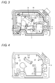
- Fig. 4 is a view illustrating the case 2 included in the optical sensor 100 of the embodiment of the present invention. Referring to Figs. 3 and 4 , the light projecting module 4, light receiving lens unit 7, and the light receiving unit 8 are each independently and directly fixed to the case 2.
- the circuit board 10 is a rigid flexible board.
- the circuit board 10 is accommodated in the case 2 while a flexible print board is bent.
- the circuit board 10 is disposed while separated from the light projecting module 4 and the light receiving lens unit 7. Additionally, the circuit board 10 is disposed away from the light receiving unit 8 (the light receiving element).
- a groove or a protrusion is formed in the case 2 in order to determine the positions of the light projecting module 4, the light receiving lens unit 7, and the light receiving unit 8 in the case 2.
- the light projecting module 4, the light receiving lens unit 7, and the light receiving unit 8 are fixed to the case 2 by an ultraviolet-curing adhesive 11 (also called a UV adhesive).
- an ultraviolet-curing adhesive 11 also called a UV adhesive.
- a rough area to which the ultraviolet-curing adhesive is applied is indicated by a broken-line surrounding.
- the area to which the ultraviolet-curing adhesive 11 is applied is indicated only for the light receiving lens unit 7 and the light receiving unit 8 in Fig. 3 .
- the ultraviolet-curing adhesive has a small linear expansion coefficient. Temperature compensation can be ensured (a position change due to a temperature is prevented) by fixing the light receiving unit 8 using the ultraviolet-curing adhesive. It is difficult to fix the circuit board to the case using the ultraviolet-curing adhesive while the light receiving element is mounted on the circuit board. In the embodiment, since the light receiving unit 8 is a light receiving element disposed while separated from the circuit board, the light receiving unit 8 can be fixed using the ultraviolet-curing adhesive 11.
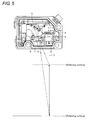
- Fig. 5 is a view explaining a disposition of the optical system in the optical sensor 100 of the embodiment of the present invention.
- a light receiving plane A of the light receiving unit 8 and a principal plane B of the light receiving lens 6 intersect each other on a certain straight line.
- the straight line is indicated by an intersection point of the two straight lines.
- a subject plane C that is in focus also intersects the light receiving plane A of the light receiving unit 8 and the principal plane B of the light receiving lens 6 on the straight line.
- the subject plane C is indicated as a straight line matched with the optical axis of the light projecting module 4.
- the light projected from the light projecting module 4 is reflected by a reflecting surface, and enter the light receiving unit 8 through the light receiving lens 6. Because the subject plane is not parallel to the principal plane of the light receiving lens, the reflecting surface located near the optical sensor 100 and the reflecting surface located distant from the optical sensor 100 can simultaneously be in focus. Accordingly, the optical sensor 100 of the embodiment of the present invention can measure, for example a height of an object. Alternatively the optical sensor 100 can be used to detect existence or non-existence of the object.
- Fig. 6 is an outside drawing of the light projecting module 4 in Fig. 1 .
- Fig. 7 is a view illustrating an inside of the light projecting module 4 in Fig. 6 .
- Fig. 8 is an exploded perspective view of the light projecting module 4 in Fig. 6 .
- the light projecting module 4 includes a light projecting lens 22, a laser diode 24 (the light emitting unit), a light projecting unit holder 20, and an LD board 26.
- the light projecting module 4 includes the light projecting unit holder 20 made of a glass-fiber reinforced resin, the light projecting lens 22 made of a resin, and the laser diode 24 that is of the light emitting unit.
- the resin similar to that of the case 2 is used for the light projecting unit holder 20, or another material having the equal linear expansion coefficient may be used.
- the light projecting lens 22 is held by and fixed to the light projecting module 4 isotropically with respect to the directions perpendicular to the optical axis. For example, after the light projecting lens 22 is press-fitted in the optical axis direction, the light projecting lens 22 is fixed while being held down in the optical axis direction or adhered thereto.
- the light projecting lens 22 may be held isotropically with respect to the directions perpendicular to the optical axis such that there is not left after the insertion the degree of movement freedom of the inside member due to the expansion in a specific or arbitrary one direction perpendicular to the optical axis. Therefore, even if the press-fitted member is made of the resin, the movement of the center position due to the temperature change becomes very small in the direction perpendicular to the optical axis.
- the light projecting unit holder 20 includes a lens holding unit 20a that holds the light projecting lens 22 and a light emitting unit holding unit 20b that holds the laser diode 24.
- the lens holding unit 20a is formed into a cylindrical shape.
- a slide hole 21 is made to the lens holding unit 20a along an extending direction of the lens holding unit 20a in order to slide the light projecting lens 22 in the lens holding unit 20a.
- the light projecting lens 22 is accommodated in the lens holding unit 20a, and the light projecting lens 22 is fixed using an ultraviolet-curing adhesive 23 while abutting on the surface perpendicular to the optical axis direction of the light projecting unit holder 20.
- the laser diode 24 is accommodated in the light emitting unit holding unit 20b.
- the laser diode 24 is press-fitted in the light emitting unit holding unit 20b, and held by the LD board 26 in the optical axis direction of the light projecting unit holder 20, thereby fixing the laser diode 24.
- a hole to which a terminal of the laser diode 24 is inserted is made in the LD board 26.
- the LD board 26 is fixed to the light emitting unit holding unit 20b using, for example an ultraviolet-curing adhesive 25 while the terminal of the laser diode 24 is inserted in the hole of the LD board 26, whereby the laser diode 24 is fixed.
- the LD board 26 acts as a holding member that fixes the light emitting unit accommodated in the light projecting unit holder 20.
- the holding member is not limited to the LD board.
- a disposition of such an optical system as the light emitting unit (for example, the laser diode), the light projecting lens, the light receiving lens, and the light receiving unit (the light receiving element) has an influence on detection performance of the optical sensor. Alignment of the optical system is adjusted during assembly of the optical sensor 100.
- the light emitting unit generates heat while emitting the light. Even if the alignment of the optical system is adjusted once, the alignment possibly deviates due to the heat generation of the light emitting unit.
- the temperature changes depending also on a usage environment. Particularly, when a position gap is generated between the light emitting unit and the light projecting lens, the detection performance of the optical sensor 100 is largely influenced because an influence on a light receiving system arises. Accordingly, it is necessary to reduce the position gap between the light emitting unit and the light projecting lens as much as possible.
- the base, the light projecting lens holder, and the light receiving lens holder are made of the glass-fiber reinforced resin.
- the base, the light projecting lens holder, and the light receiving lens holder all may be made of a resin that does not include the glass fiber.
- Fig. 9 is a view illustrating a conventional example of a configuration that reduces the position gap between the light emitting unit and the light projecting lens due to the heat generation of the light emitting unit.
- the laser diode 24, the light projecting lens 22, the light receiving lens unit 7 (the light receiving lens 6), and the light receiving unit 8 are attached to a base 30.
- the optical element is accommodated in the case 2 by attaching the base 30 to the case 2.
- the base 30 is made of metal (for example, aluminum). The heat generated by the laser diode 24 is released by the base 30. Therefore, the position gap between the laser diode 24 and the light projecting lens 22 can be reduced. However, production cost of the optical sensor increases because the number of components increases.
- the optical element is accommodated in the case 2 after once attached to the base 30.
- a user adjusts an angle of the optical sensor 100 with respect to a horizontal surface or an angle in a right-left direction of the optical sensor 100 from, for example an outer shape of the case 2.
- the detection performance for example, the detection performance in the direction perpendicular to the light projecting window of the case 2 determined from the outer shape of the case 2 degraded for such the reasons as the position gap in attaching the case 2 to the base 30.
- the degradation of the detection performance becomes problem in a detection requiring high-accuracy (for example, in the case of detecting munute height).
- the base is not required. That is, the case 2 works also as the base.
- the light projecting module 4, the light receiving lens unit 7 that holds the light receiving lens 6, and the light receiving unit 8 are directly attached to the case 2. Therefore, the number of components and assembly manhours can be reduced, so that the production cost of the optical sensor can be reduced.
- the base is made of metal from the viewpoint of the heat release as described above.
- downsizing and weight reduction of the optical sensor can be achieved by eliminating the necessity of the base.
- a possibility of degrading the optical sensor detection performance determined from the outer shape of the case 2 is reduced by eliminating the necessity of the base. Accordingly, the adjustment (for example, the adjustments of the position, the angle with respect to the horizontal surface, and the angle in the right-left direction) of the optical sensor can easily be performed in order to ensure the detection accuracy.
- the case 2 is made of the material having the small linear expansion coefficient.
- the case 2 is made of a resin having the linear expansion coefficient that is less than or equal to the linear expansion coefficient of a die-casting metal.
- the expansion of the case 2 due to the heat generation of the light emitting unit (the laser diode 24) can be reduced as much as possible. Accordingly, misalignment can be reduced among the light projecting module 4, the light receiving unit 8, and the light receiving lens unit 7.
- the base is made of aluminum, and produced by, for example die-casting.
- the case 2 is made of the resin having the linear expansion coefficient that is less than or equal to the linear expansion coefficient of the die-casting metal, which allows the thermal expansion of the case 2 due to the heat generation of the laser diode 24 to be equal to or less than the thermal expansion of the base member. Accordingly, misalignment can be reduced among the light projecting module 4, the light receiving unit 8, and the light receiving lens unit 7 which are directly fixed to the case 2.
- the light emitting unit (the laser diode 24) and the light projecting lens 22 are integral with the light projecting module 4.
- the position gap between the laser diode 24 and the light projecting lens 22 due to the heat generation of the laser diode 24 during the emission of the laser diode 24 or the change of ambient temperature can be reduced because the laser diode 24 and the light projecting lens 22 are integral with the light projecting module 4.
- the light projecting unit holder 20 that holds the laser diode 24 and the light projecting lens 22 is made of a material having the small linear expansion coefficient.
- the light projecting unit holder 20 is made of the resin having the linear expansion coefficient that is less than or equal to the linear expansion coefficient of the die-casting metal.
- the position gap between the laser diode 24 and the light projecting lens 22 can be reduced when the temperature of the laser diode 24 rises.
- the light projecting unit holder 20 can be made of, for example glass-fiber reinforced PPE (polyphenylen ether).
- the light projecting lens 22 is held in the lens holding unit 20a of the light projecting unit holder 20. Before the light projecting lens 22 is fixed, the light projecting lens 22 can be slid in the lens holding unit 20a. Therefore, a distance from the laser diode 24 to the light projecting lens 22 can be adjusted.
- the optical sensor 100 includes the semiconductor integrated circuit.
- the semiconductor integrated circuit also generates heat during operation, similarly to the laser diode. Accordingly, it is necessary that the semiconductor integrated circuit be disposed in the case 2 while separated from the optical system as much as possible.
- the semiconductor integrated circuit is preferably disposed distant from the light projecting module 4.
- Figs. 10A and 10B are schematic diagrams explaining the disposition relationship between the semiconductor integrated circuit and the light projecting module.
- Fig. 10A is a perspective view illustrating the inside of the case when viewed from above the light projecting module 4
- Fig. 10B is a perspective view illustrating the inside of the case when viewed from an optical axis direction of the light projecting module 4.
- the light projecting module 4 is disposed close to one side surface 2c of the case 2.
- a semiconductor integrated circuit 40a can be disposed close to another side surface 2d opposed to the side surface 2c of the case 2.
- the light projecting module 4 is attached to a side surface 2e of the case 2.
- a semiconductor integrated circuit 40b can be disposed close to side surfaces 2d and 2f of the case 2.
- the side surface 2f is opposed to the side surface 2e.
- the circuit board on which the semiconductor integrated circuits 40a or 40b are mounted is not illustrated for the purpose of easy understanding of the positions of the semiconductor integrated circuits 40a and 40b.
- Fig. 11 is a flowchart for explaining a method for assembling the optical sensor of the embodiment of the present invention. Particularly, a method for fixing the optical component to the case is explained in Fig. 11 .
- the light projecting module 4 is assembled and adjusted. Specifically, the laser diode 24 and the light projecting lens 22 are inserted in the light projecting unit holder 20.
- the LD board 26 is attached to the light projecting unit holder 20.
- the ultraviolet-curing adhesive 25 is applied to the light projecting unit holder 20 and the LD board 26, and the ultraviolet-curing adhesive 25 is irradiated with an ultraviolet ray. Therefore, the laser diode 24 is held by the light projecting unit holder 20.
- the position of the light projecting lens 22 is adjusted by moving the light projecting lens 22 in the lens holding unit 20a.
- the ultraviolet-curing adhesive 23 is applied to the lens holding unit 20a (the position of the slide hole 21 corresponding to the position of the light projecting lens 22) for fixing the light projecting lens 22, and the light projecting lens 22 is fixed by irradiating the ultraviolet-curing adhesive 23 with the ultraviolet ray.
- Step S2 the light receiving unit 8 is attached to the case 2.
- Step S3 the light projecting module 4 is attached to the case 2.
- Step S4 the alignment of the receiving lens unit 7 is performed in the case 2, and the receiving lens unit 7 is attached to the case 2.
- the possibility of degrading the optical sensor detection performance determined from the outer shape of the case 2 can also be reduced from this viewpoint.
Landscapes
- Physics & Mathematics (AREA)
- General Physics & Mathematics (AREA)
- Engineering & Computer Science (AREA)
- Electromagnetism (AREA)
- Spectroscopy & Molecular Physics (AREA)
- Computer Networks & Wireless Communication (AREA)
- Radar, Positioning & Navigation (AREA)
- Remote Sensing (AREA)
- Photometry And Measurement Of Optical Pulse Characteristics (AREA)
- Photo Coupler, Interrupter, Optical-To-Optical Conversion Devices (AREA)
- Lens Barrels (AREA)
Abstract
Description
- The present invention relates to an optical sensor, particularly to a structure of an optical sensor.
- Conventionally, various configurations have been proposed for the optical sensor. For example, Japanese Unexamined Patent Publication No.
2001-267626 - Generally the optical sensor includes not only the light projecting unit but also a light receiving unit. As used herein, the light receiving unit includes optical components, such as a light receiving element and a light receiving lens, which receive light.
- Accuracy of positions of the light projecting unit and the light receiving unit in a case has an influence on performance of the optical sensor. For example, the light projecting unit emits the light to generate heat. The positions of the light projecting unit and the light receiving unit are changed by the heat to possibly change the performance of the optical sensor. However, Japanese Unexamined Patent Publication No.
2001-267626 - The present invention has been devised to solve the problems described above, and an object thereof is to provide an optical sensor that can ensure the accuracy of the positions of the light projecting unit and the light receiving unit in the case.
- In accordance with one aspect of the present invention, an optical sensor includes: a case; a light projecting module that includes a light emitting unit and a light projecting lens, and integrates the unit and the lens; a light receiving unit configured to receive reflected light of light projected from the light projecting module; and a light receiving lens unit configured to form an image of the reflected light on the light receiving unit. In the optical sensor, the light projecting module, the light receiving unit, and the light receiving lens unit are each independently and directly fixed to the case.
- According to the configuration, the light emitting unit and the light projecting lens are integrated by the light projecting module. Therefore, a position gap between the light emitting unit and the light projecting lens is reduced as much as possible. Necessity of a base member (for example, metal) to which the light projecting module, the light receiving unit, and the light receiving lens unit are attached is eliminated because the light projecting module, the light receiving unit, and the light receiving lens unit are independently and directly fixed to the case. Additionally, weight reduction and downsizing of the optical sensor can be achieved by eliminating the necessity of the base member.
- Preferably, in the light projecting module, the light projecting lens is held by and fixed to a light projecting lens holder isotropically with respect to directions perpendicular to an optical axis defined by the light projecting lens and the light emitting unit. The light receiving lens unit includes a light receiving lens and a light receiving lens holder configured to hold the light receiving lens. The light receiving lens is held by and fixed to the light receiving lens holder isotropically with respect to directions perpendicular to an optical axis defined by the light receiving lens and the light receiving unit. The base, the light projecting lens holder, and the light receiving lens holder are all made of a resin or a glass-fiber reinforced resin. Here, "held isotropically with respect to the directions perpendicular to the optical axis" means that all holding forces that hold the lens in place and that act in a direction perpendicular to the optical axis have the same magnitude. In other words, any two holding forces acting on the lens from the edge of the lens towards the center of the lens have the same magnitude, so as not to shift the center of the lens.
- According to the configuration, because the base, the light projecting lens holder, and the light receiving lens holder have the substantially identical linear expansion coefficient, expansion and contraction are generated also by a temperature change while the disposition relationship among the light emitting unit, the light projecting lens, the light receiving unit, and the light receiving lens is maintained at a similar shape. Therefore, a relationship between a light projecting optical axis, defined by the dispositions of the light emitting unit and the light projecting lens, and a light receiving optical axis, defined by the dispositions of the light receiving unit and the light receiving lens, is maintained to stabilize measurement accuracy.
- Preferably, the case is made of a glass-fiber reinforced resin. The light projecting lens is made of a resin. The light projecting lens holder is made of the glass-fiber reinforced resin. The light receiving lens unit is made of the resin. The light receiving lens holder is made of the glass-fiber reinforced resin.
- According to the configuration, the case is made of the glass-fiber reinforced resin to enhance shape accuracy. Therefore, the measurement accuracy can stably be maintained even if the lens is made of a usual resin having the linear expansion coefficient different from that of the case.
- Preferably, the case is made of a resin having a linear expansion coefficient that is less than or equal to a linear expansion coefficient of a die-casting metal.
- According to the configuration, expansion of the case due to the heat generation of the light emitting unit is reduced as much as possible. Accordingly, misalignment among the light projecting module, the light receiving unit, and the light receiving lens unit can be reduced. For example, the base member is produced by die-casting using a die-casting metal (such as aluminum, but may also be zinc and magnesium). Accordingly, the case is made of the resin having the linear expansion coefficient that is less than or equal to the linear expansion coefficient of the die-casting metal, which allows the case thermal expansion due to the heat generation of the light emitting unit to be reduced to less than or equal to the base member. Therefore, the misalignment among the light projecting module, the light receiving unit, and the light receiving lens unit, which are directly fixed to the case, can be reduced.
- Preferably, the light projecting module includes: a light projecting unit holder in which the light emitting unit and the light projecting lens are accommodated; and a holding member configured to fix the light emitting unit accommodated in the light projecting unit holder. The holding member and the light projecting lens are fixed to the light projecting unit holder using an ultraviolet-curing adhesive. The light receiving unit includes a light receiving element that is disposed away from a circuit board, and the light receiving element is fixed to the case using the ultraviolet-curing adhesive.
- According to the configuration, the light receiving element or the light emitting unit can be fixed without applying a stress. Usually the ultraviolet-curing adhesive (also called a UV adhesive) has a small linear expansion coefficient. Temperature compensation can be ensured (a position change due to a temperature is prevented) by fixing the light receiving element or the light emitting unit using the ultraviolet-curing adhesive. The light emitting unit is held by a holding plate after the light emitting unit is, for example press-fitted in the light projecting unit holder. The holding plate and light projecting unit holder are adhered to each other using the UV adhesive to be able to fix the light emitting unit. It is difficult that the light receiving unit in which the light receiving element and the processing board are integral with each other is fixed to the case using the ultraviolet-curing adhesive. Only the light receiving element can be fixed to the case using the ultraviolet-curing adhesive by separating the light receiving element and the circuit board from each other.
- Preferably, the light projecting unit holder is made of a resin having a linear expansion coefficient that is less than or equal to a linear expansion coefficient of a die-casting metal.
- According to the configuration, the expansion of the light projecting unit holder due to the heat generation of the light emitting unit is reduced as much as possible. Accordingly, the misalignment between the light emitting unit and the light projecting lens can be reduced.
- Preferably, the light projecting module, the light receiving lens, and the light receiving unit are disposed such that a principal plane of the light receiving lens included in the light receiving lens unit, a light receiving plane of the light receiving unit, and the optical axis of the light projecting module intersect one another at one point.
- According to the configuration, what is called a Scheimpflug disposition is implemented. Preferably, the optical sensor further includes a semiconductor integrated circuit configured to process a light reception signal from the light receiving unit. In the optical sensor, the semiconductor integrated circuit is disposed in the case while separated from the light projecting module.
- According to the configuration, a possibility that the optical component is misaligned by the heat generated by the semiconductor integrated circuit can be reduced because the semiconductor integrated circuit that is of a potential heat source is separated from the light projecting module.
- Preferably, the light projecting unit holder includes a cylindrical unit in which the light projecting lens is configured to be able to slide inside thereof. The light projecting lens is fixed to an inside of the cylindrical unit.
- According to the configuration, the light projecting lens can easily be aligned after the light projecting lens is inserted in the cylindrical unit of the light projecting unit holder.
- According to the prevent invention, the optical sensor that can ensure the accuracy of the positions of the light projecting unit and the light receiving unit in the case can be made.
-
-
Fig. 1 is a perspective view illustrating an appearance of an optical sensor according to an embodiment of the present invention; -
Fig. 2 is an exploded perspective view of the optical sensor inFig. 1 ; -
Fig. 3 is a view illustrating a configuration of an optical system in the optical sensor of the embodiment of the present invention; -
Fig. 4 is a view illustrating a case included in the optical sensor of the embodiment of the present invention; -
Fig. 5 is a view explaining a disposition of the optical system in the optical sensor of the embodiment of the present invention; -
Fig. 6 is an outside drawing of a light projecting module inFig. 1 ; -
Fig. 7 is a view illustrating an inside of the light projecting module inFig. 6 ; -
Fig. 8 is an exploded perspective view of the light projecting module inFig. 6 ; -
Fig. 9 is a view illustrating a conventional example of a configuration that reduces a position gap between a light emitting unit and the light projecting lens due to heat generation of the light emitting unit; -
Figs. 10A and 10B are schematic diagrams explaining a disposition relationship between a semiconductor integrated circuit and the light projecting module; and -
Fig. 11 is a flowchart for explaining a method for assembling the optical sensor of the embodiment of the present invention. - Hereinafter, an embodiment of the present invention will be described in detail with reference to the drawings. In the drawings, the identical or equivalent component is designated by the identical numeral, and the overlapping description is neglected.
-
Fig. 1 is a perspective view illustrating an appearance of anoptical sensor 100 according to an embodiment of the present invention.Fig. 2 is an exploded perspective view of theoptical sensor 100 inFig. 1 . Referring toFigs. 1 and2 , theoptical sensor 100 detects, for example existence or non-existence of an object by light projection and light reception. There is no particular limitation to a use application of theoptical sensor 100. - The
optical sensor 100 includes acase 2, alight projecting module 4, a light receivinglens unit 7 including alight receiving lens 6, alight receiving unit 8,circuit boards cable 14. - The
case 2 accommodates the light projectingmodule 4, the light receivinglens unit 7 including thelight receiving lens 6 and a light receiving lens holder, thelight receiving unit 8, and thecircuit boards light projecting window 2a and alight receiving window 2b are formed in thecase 2. - The
case 2 is made of a resin having a small linear expansion coefficient. For example, thecase 2 is made of a glass-fiber reinforced resin. For example, glass-fiber reinforced PBT (polybutylene terephthalate) can be used as the glass-fiber reinforced resin. A resin having the linear expansion coefficient that is less than or equal to the linear expansion coefficient of a die-casting metal (for example, aluminum, but may also be zinc and magnesium) can be used. For example, because an aluminum die-casting alloy has the linear expansion coefficient of about 2×10⁻⁵/°C, a material having the similar linear expansion coefficient can be used in the glass-fiber reinforced PBT that is of the material for thecase 2. The material of thecase 2 is not limited to PBT. - The light projecting
module 4 includes a light emitting unit that emits light and a light projecting lens. The light emitted from the light emitting unit is projected to the outside of theoptical sensor 100 from thelight projecting window 2a of thecase 2 through the light projecting lens. The light projected from theoptical sensor 100 is reflected, and enter thelight receiving lens 6 through thelight receiving window 2b of thecase 2. The light entered thelight receiving lens 6 forms an image on a light receiving plane of thelight receiving unit 8. A light receiving element such as a CMOS sensor or a CCD sensor is used as thelight receiving unit 8. - The light receiving
lens unit 7 includes thelight receiving lens 6 that is made of a resin and a light receiving lens holder that is made of a glass-fiber reinforced resin to hold thelight receiving lens 6. For example, the light receiving lens holder is made of the resin similar to that of thecase 2, or another material having the similar linear expansion coefficient may be used. Thelight receiving lens 6 is held by and fixed to the light receiving lens holder isotropically with respect to directions perpendicular to an optical axis. For example, after thelight receiving lens 6 is press-fitted in an optical axis direction, thelight receiving lens 6 is fixed while being held down in the optical axis direction or adhered thereto. In the fixing, thelight receiving lens 6 may be held isotropically with respect to the directions perpendicular to the optical axis such that there is not left after the insertion a degree of movement freedom of an inside member due to the expansion in a specific or arbitrary one direction perpendicular to the optical axis. Therefore, even if the press-fitted member is made of the resin, the movement of a center position due to a temperature change becomes very small in the direction perpendicular to the optical axis. - The
circuit boards light receiving unit 8. For example, a power supply circuit and a signal processing circuit are mounted on thecircuit boards cable 14. -
Fig. 3 is a view illustrating a configuration of an optical system in theoptical sensor 100 of the embodiment of the present invention.Fig. 4 is a view illustrating thecase 2 included in theoptical sensor 100 of the embodiment of the present invention. Referring toFigs. 3 and 4 , thelight projecting module 4, light receivinglens unit 7, and thelight receiving unit 8 are each independently and directly fixed to thecase 2. - The
circuit board 10 is a rigid flexible board. Thecircuit board 10 is accommodated in thecase 2 while a flexible print board is bent. Thecircuit board 10 is disposed while separated from the light projectingmodule 4 and the light receivinglens unit 7. Additionally, thecircuit board 10 is disposed away from the light receiving unit 8 (the light receiving element). - For example, a groove or a protrusion is formed in the
case 2 in order to determine the positions of the light projectingmodule 4, the light receivinglens unit 7, and thelight receiving unit 8 in thecase 2. The light projectingmodule 4, the light receivinglens unit 7, and thelight receiving unit 8 are fixed to thecase 2 by an ultraviolet-curing adhesive 11 (also called a UV adhesive). InFig. 3 and the subsequent drawings, a rough area to which the ultraviolet-curing adhesive is applied is indicated by a broken-line surrounding. In order to avoid complication of the drawings, the area to which the ultraviolet-curingadhesive 11 is applied is indicated only for the light receivinglens unit 7 and thelight receiving unit 8 inFig. 3 . - Generally the ultraviolet-curing adhesive has a small linear expansion coefficient. Temperature compensation can be ensured (a position change due to a temperature is prevented) by fixing the
light receiving unit 8 using the ultraviolet-curing adhesive. It is difficult to fix the circuit board to the case using the ultraviolet-curing adhesive while the light receiving element is mounted on the circuit board. In the embodiment, since thelight receiving unit 8 is a light receiving element disposed while separated from the circuit board, thelight receiving unit 8 can be fixed using the ultraviolet-curingadhesive 11. -
Fig. 5 is a view explaining a disposition of the optical system in theoptical sensor 100 of the embodiment of the present invention. Referring toFig. 5 , a light receiving plane A of thelight receiving unit 8 and a principal plane B of thelight receiving lens 6 intersect each other on a certain straight line. InFig. 5 , the straight line is indicated by an intersection point of the two straight lines. According to a Scheimpflug principle, a subject plane C that is in focus also intersects the light receiving plane A of thelight receiving unit 8 and the principal plane B of thelight receiving lens 6 on the straight line. InFig. 5 , the subject plane C is indicated as a straight line matched with the optical axis of the light projectingmodule 4. - The light projected from the light projecting
module 4 is reflected by a reflecting surface, and enter thelight receiving unit 8 through thelight receiving lens 6. Because the subject plane is not parallel to the principal plane of the light receiving lens, the reflecting surface located near theoptical sensor 100 and the reflecting surface located distant from theoptical sensor 100 can simultaneously be in focus. Accordingly, theoptical sensor 100 of the embodiment of the present invention can measure, for example a height of an object. Alternatively theoptical sensor 100 can be used to detect existence or non-existence of the object. -
Fig. 6 is an outside drawing of the light projectingmodule 4 inFig. 1 .Fig. 7 is a view illustrating an inside of the light projectingmodule 4 inFig. 6 .Fig. 8 is an exploded perspective view of the light projectingmodule 4 inFig. 6 . Referring toFigs. 6 to 8 , thelight projecting module 4 includes alight projecting lens 22, a laser diode 24 (the light emitting unit), a light projectingunit holder 20, and anLD board 26. - The light projecting
module 4 includes the light projectingunit holder 20 made of a glass-fiber reinforced resin, thelight projecting lens 22 made of a resin, and thelaser diode 24 that is of the light emitting unit. For example, the resin similar to that of thecase 2 is used for the light projectingunit holder 20, or another material having the equal linear expansion coefficient may be used. Thelight projecting lens 22 is held by and fixed to the light projectingmodule 4 isotropically with respect to the directions perpendicular to the optical axis. For example, after thelight projecting lens 22 is press-fitted in the optical axis direction, thelight projecting lens 22 is fixed while being held down in the optical axis direction or adhered thereto. In the fixing, thelight projecting lens 22 may be held isotropically with respect to the directions perpendicular to the optical axis such that there is not left after the insertion the degree of movement freedom of the inside member due to the expansion in a specific or arbitrary one direction perpendicular to the optical axis. Therefore, even if the press-fitted member is made of the resin, the movement of the center position due to the temperature change becomes very small in the direction perpendicular to the optical axis. Specifically, the light projectingunit holder 20 includes alens holding unit 20a that holds thelight projecting lens 22 and a light emittingunit holding unit 20b that holds thelaser diode 24. Thelens holding unit 20a is formed into a cylindrical shape. Aslide hole 21 is made to thelens holding unit 20a along an extending direction of thelens holding unit 20a in order to slide thelight projecting lens 22 in thelens holding unit 20a. - The
light projecting lens 22 is accommodated in thelens holding unit 20a, and thelight projecting lens 22 is fixed using an ultraviolet-curingadhesive 23 while abutting on the surface perpendicular to the optical axis direction of the light projectingunit holder 20. Similarly, thelaser diode 24 is accommodated in the light emittingunit holding unit 20b. For example, thelaser diode 24 is press-fitted in the light emittingunit holding unit 20b, and held by theLD board 26 in the optical axis direction of the light projectingunit holder 20, thereby fixing thelaser diode 24. - A hole to which a terminal of the
laser diode 24 is inserted is made in theLD board 26. TheLD board 26 is fixed to the light emittingunit holding unit 20b using, for example an ultraviolet-curingadhesive 25 while the terminal of thelaser diode 24 is inserted in the hole of theLD board 26, whereby thelaser diode 24 is fixed. TheLD board 26 acts as a holding member that fixes the light emitting unit accommodated in the light projectingunit holder 20. However, the holding member is not limited to the LD board. - A disposition of such an optical system as the light emitting unit (for example, the laser diode), the light projecting lens, the light receiving lens, and the light receiving unit (the light receiving element) has an influence on detection performance of the optical sensor. Alignment of the optical system is adjusted during assembly of the
optical sensor 100. - On the other hand, the light emitting unit generates heat while emitting the light. Even if the alignment of the optical system is adjusted once, the alignment possibly deviates due to the heat generation of the light emitting unit. The temperature changes depending also on a usage environment. Particularly, when a position gap is generated between the light emitting unit and the light projecting lens, the detection performance of the
optical sensor 100 is largely influenced because an influence on a light receiving system arises. Accordingly, it is necessary to reduce the position gap between the light emitting unit and the light projecting lens as much as possible. - In the embodiment, the base, the light projecting lens holder, and the light receiving lens holder are made of the glass-fiber reinforced resin. Alternatively, the base, the light projecting lens holder, and the light receiving lens holder all may be made of a resin that does not include the glass fiber.
-
Fig. 9 is a view illustrating a conventional example of a configuration that reduces the position gap between the light emitting unit and the light projecting lens due to the heat generation of the light emitting unit. Referring toFig. 9 , thelaser diode 24, thelight projecting lens 22, the light receiving lens unit 7 (the light receiving lens 6), and thelight receiving unit 8 are attached to abase 30. The optical element is accommodated in thecase 2 by attaching the base 30 to thecase 2. - The
base 30 is made of metal (for example, aluminum). The heat generated by thelaser diode 24 is released by thebase 30. Therefore, the position gap between thelaser diode 24 and thelight projecting lens 22 can be reduced. However, production cost of the optical sensor increases because the number of components increases. - The optical element is accommodated in the
case 2 after once attached to thebase 30. For example, in placing theoptical sensor 100 in a production line, a user adjusts an angle of theoptical sensor 100 with respect to a horizontal surface or an angle in a right-left direction of theoptical sensor 100 from, for example an outer shape of thecase 2. Possibly the detection performance (for example, the detection performance in the direction perpendicular to the light projecting window of the case 2) determined from the outer shape of thecase 2 degraded for such the reasons as the position gap in attaching thecase 2 to thebase 30. Possibly the degradation of the detection performance becomes problem in a detection requiring high-accuracy (for example, in the case of detecting munute height). - On the other hand, in the embodiment of the present invention, the base is not required. That is, the
case 2 works also as the base. The light projectingmodule 4, the light receivinglens unit 7 that holds thelight receiving lens 6, and thelight receiving unit 8 are directly attached to thecase 2. Therefore, the number of components and assembly manhours can be reduced, so that the production cost of the optical sensor can be reduced. - The base is made of metal from the viewpoint of the heat release as described above. In the embodiment of the present invention, downsizing and weight reduction of the optical sensor can be achieved by eliminating the necessity of the base.
- A possibility of degrading the optical sensor detection performance determined from the outer shape of the
case 2 is reduced by eliminating the necessity of the base. Accordingly, the adjustment (for example, the adjustments of the position, the angle with respect to the horizontal surface, and the angle in the right-left direction) of the optical sensor can easily be performed in order to ensure the detection accuracy. - The
case 2 is made of the material having the small linear expansion coefficient. In one embodiment, thecase 2 is made of a resin having the linear expansion coefficient that is less than or equal to the linear expansion coefficient of a die-casting metal. In the configuration, the expansion of thecase 2 due to the heat generation of the light emitting unit (the laser diode 24) can be reduced as much as possible. Accordingly, misalignment can be reduced among the light projectingmodule 4, thelight receiving unit 8, and the light receivinglens unit 7. Usually the base is made of aluminum, and produced by, for example die-casting. Thecase 2 is made of the resin having the linear expansion coefficient that is less than or equal to the linear expansion coefficient of the die-casting metal, which allows the thermal expansion of thecase 2 due to the heat generation of thelaser diode 24 to be equal to or less than the thermal expansion of the base member. Accordingly, misalignment can be reduced among the light projectingmodule 4, thelight receiving unit 8, and the light receivinglens unit 7 which are directly fixed to thecase 2. - Further according to the embodiment of the present invention, the light emitting unit (the laser diode 24) and the
light projecting lens 22 are integral with the light projectingmodule 4. The position gap between thelaser diode 24 and thelight projecting lens 22 due to the heat generation of thelaser diode 24 during the emission of thelaser diode 24 or the change of ambient temperature can be reduced because thelaser diode 24 and thelight projecting lens 22 are integral with the light projectingmodule 4. - Preferably the light projecting
unit holder 20 that holds thelaser diode 24 and thelight projecting lens 22 is made of a material having the small linear expansion coefficient. Similarly to thecase 2, the light projectingunit holder 20 is made of the resin having the linear expansion coefficient that is less than or equal to the linear expansion coefficient of the die-casting metal. - Therefore, the position gap between the
laser diode 24 and thelight projecting lens 22 can be reduced when the temperature of thelaser diode 24 rises. For example, the light projectingunit holder 20 can be made of, for example glass-fiber reinforced PPE (polyphenylen ether). - The
light projecting lens 22 is held in thelens holding unit 20a of the light projectingunit holder 20. Before thelight projecting lens 22 is fixed, thelight projecting lens 22 can be slid in thelens holding unit 20a. Therefore, a distance from thelaser diode 24 to thelight projecting lens 22 can be adjusted. - As described above, the
optical sensor 100 includes the semiconductor integrated circuit. The semiconductor integrated circuit also generates heat during operation, similarly to the laser diode. Accordingly, it is necessary that the semiconductor integrated circuit be disposed in thecase 2 while separated from the optical system as much as possible. Particularly, the semiconductor integrated circuit is preferably disposed distant from the light projectingmodule 4. -
Figs. 10A and 10B are schematic diagrams explaining the disposition relationship between the semiconductor integrated circuit and the light projecting module.Fig. 10A is a perspective view illustrating the inside of the case when viewed from above the light projectingmodule 4, andFig. 10B is a perspective view illustrating the inside of the case when viewed from an optical axis direction of the light projectingmodule 4. Referring toFig. 10 , for example, thelight projecting module 4 is disposed close to oneside surface 2c of thecase 2. A semiconductor integratedcircuit 40a can be disposed close to anotherside surface 2d opposed to theside surface 2c of thecase 2. The light projectingmodule 4 is attached to aside surface 2e of thecase 2. A semiconductor integratedcircuit 40b can be disposed close toside surfaces case 2. Theside surface 2f is opposed to theside surface 2e. InFig. 10 , the circuit board on which the semiconductor integratedcircuits circuits -
Fig. 11 is a flowchart for explaining a method for assembling the optical sensor of the embodiment of the present invention. Particularly, a method for fixing the optical component to the case is explained inFig. 11 . Referring toFig. 11 , in Step S1, thelight projecting module 4 is assembled and adjusted. Specifically, thelaser diode 24 and thelight projecting lens 22 are inserted in the light projectingunit holder 20. TheLD board 26 is attached to the light projectingunit holder 20. The ultraviolet-curingadhesive 25 is applied to the light projectingunit holder 20 and theLD board 26, and the ultraviolet-curingadhesive 25 is irradiated with an ultraviolet ray. Therefore, thelaser diode 24 is held by the light projectingunit holder 20. - The position of the
light projecting lens 22 is adjusted by moving thelight projecting lens 22 in thelens holding unit 20a. When the position of thelight projecting lens 22 is determined, the ultraviolet-curingadhesive 23 is applied to thelens holding unit 20a (the position of theslide hole 21 corresponding to the position of the light projecting lens 22) for fixing thelight projecting lens 22, and thelight projecting lens 22 is fixed by irradiating the ultraviolet-curingadhesive 23 with the ultraviolet ray. - In Step S2, the
light receiving unit 8 is attached to thecase 2. In Step S3, thelight projecting module 4 is attached to thecase 2. - In Step S4, the alignment of the receiving
lens unit 7 is performed in thecase 2, and the receivinglens unit 7 is attached to thecase 2. - According to the embodiment of the present invention, it is not necessary to adjust the alignment between the light projecting
lens 22 and thelaser diode 24 after the light projectingmodule 4 is attached to thecase 2. The possibility of degrading the optical sensor detection performance determined from the outer shape of thecase 2 can also be reduced from this viewpoint. - The embodiment is described only by way of example, and should be considered not restrictive. The scope of the present invention is expressed not by the above description but by the claims, and it is intended that the meanings equivalent to the claims and all the changes within the claims are included in the present invention.
Claims (9)
- An optical sensor comprising:a case;a light projecting module that comprises a light emitting unit, a light projecting lens, and a light projecting lens holder configured to hold the light projecting lens;a light receiving unit configured to receive reflected light of light projected from the light projecting module; anda light receiving lens unit configured to form an image of the reflected light on the light receiving unit,wherein the light projecting module, the light receiving unit, and the light receiving lens unit are each independently and directly fixed to the case.
- The optical sensor according to claim 1, wherein, in the light projecting module, the light projecting lens is held by and fixed to the light projecting lens holder isotropically with respect to directions perpendicular to an optical axis defined by the light projecting lens and the light emitting unit,
the light receiving lens unit comprises a light receiving lens and a light receiving lens holder configured to hold the light receiving lens, the light receiving lens is held by and fixed to the light receiving lens holder isotropically with respect to directions perpendicular to an optical axis defined by the light receiving lens and the light receiving unit, and
the base, the light projecting lens holder, and the light receiving lens holder are all made of a resin or a glass-fiber reinforced resin. - The optical sensor according to claim 2, wherein the case is made of a glass-fiber reinforced resin,
the light projecting lens is made of a resin,
the light projecting lens holder is made of the glass-fiber reinforced resin, the light receiving lens unit is made of the resin, and
the light receiving lens holder is made of the glass-fiber reinforced resin. - The optical sensor according to any one of claims 1 to 3, wherein the case is made of a resin having a linear expansion coefficient that is less than or equal to a linear expansion coefficient of a die-casting metal.
- The optical sensor according to any one of claims 1 to 4, wherein the light projecting module comprises:a light projecting unit holder in which the light emitting unit and the light projecting lens are accommodated; anda holding member configured to fix the light emitting unit accommodated in the light projecting unit holder,the holding member and the light projecting lens are fixed to the light projecting unit holder using an ultraviolet-curing adhesive,the light receiving unit comprises a light receiving element that is disposed away from a circuit board, andthe light receiving element is fixed to the case using the ultraviolet-curing adhesive.
- The optical sensor according to claim 5, wherein the light projecting unit holder is made of a resin having a linear expansion coefficient that is less than or equal to a linear expansion coefficient of a die-casting metal.
- The optical sensor according to any one of claims 1 to 6, wherein the light projecting module, the light receiving lens, and the light receiving unit are disposed such that a principal plane of the light receiving lens comprised in the light receiving lens unit, a light receiving plane of the light receiving unit, and the optical axis of the light projecting module intersect one another at one point.
- The optical sensor according to any one of claims 1 to 7, further comprising a semiconductor integrated circuit configured to process a light reception signal from the light receiving unit,
wherein the semiconductor integrated circuit is disposed in the case while separated from the light projecting module. - The optical sensor according to claim 2 or 5, wherein the light projecting unit holder comprises a cylindrical unit in which the light projecting lens is configured to be able to slide inside thereof, and
the light projecting lens is fixed to an inside of the cylindrical unit.
Applications Claiming Priority (1)
| Application Number | Priority Date | Filing Date | Title |
|---|---|---|---|
| JP2012239571A JP6142501B2 (en) | 2012-10-30 | 2012-10-30 | Optical sensor |
Publications (2)
| Publication Number | Publication Date |
|---|---|
| EP2728378A1 true EP2728378A1 (en) | 2014-05-07 |
| EP2728378B1 EP2728378B1 (en) | 2018-11-07 |
Family
ID=49231344
Family Applications (1)
| Application Number | Title | Priority Date | Filing Date |
|---|---|---|---|
| EP13185879.7A Not-in-force EP2728378B1 (en) | 2012-10-30 | 2013-09-25 | Optical sensor |
Country Status (4)
| Country | Link |
|---|---|
| US (2) | US9448106B2 (en) |
| EP (1) | EP2728378B1 (en) |
| JP (1) | JP6142501B2 (en) |
| CN (1) | CN103792638B (en) |
Cited By (1)
| Publication number | Priority date | Publication date | Assignee | Title |
|---|---|---|---|---|
| US20190094657A1 (en) * | 2016-06-10 | 2019-03-28 | Fujitsu Frontech Limited | Imaging apparatus |
Families Citing this family (15)
| Publication number | Priority date | Publication date | Assignee | Title |
|---|---|---|---|---|
| JP2763053B2 (en) | 1993-08-28 | 1998-06-11 | 大宇電子株式會▲社▼ | Gear press fixing device for small motor |
| DE102015104212A1 (en) * | 2015-03-20 | 2016-09-22 | Valeo Schalter Und Sensoren Gmbh | Lens device for an optoelectronic sensor of a motor vehicle with fastening device, optoelectronic sensor, motor vehicle and method |
| DE102015109775B3 (en) * | 2015-06-18 | 2016-09-22 | RobArt GmbH | Optical triangulation sensor for distance measurement |
| JP6620983B2 (en) * | 2015-12-28 | 2019-12-18 | パナソニックIpマネジメント株式会社 | Particle detection sensor |
| CN105897237B (en) * | 2016-05-30 | 2018-11-13 | 星宇电子(宁波)有限公司 | A kind of retroreflecting optoelectronic switch |
| JP6852477B2 (en) * | 2017-03-13 | 2021-03-31 | オムロン株式会社 | Sensor equipment |
| JP7028607B2 (en) * | 2017-11-06 | 2022-03-02 | 株式会社ディスコ | Cutting equipment |
| US10704904B2 (en) * | 2018-03-20 | 2020-07-07 | Pixart Imaging Inc. | Distance detection device |
| JP7119772B2 (en) * | 2018-08-27 | 2022-08-17 | オムロン株式会社 | light sensor |
| CN114270537B (en) * | 2019-08-27 | 2024-01-19 | 三菱电机株式会社 | Light sensor module and method of manufacturing light sensor module |
| WO2021100356A1 (en) * | 2019-11-18 | 2021-05-27 | 株式会社村田製作所 | Optical sensor |
| WO2021117570A1 (en) * | 2019-12-09 | 2021-06-17 | パイオニア株式会社 | Sensor device |
| US12429414B2 (en) * | 2020-01-31 | 2025-09-30 | Kidde Fire Protection, Llc | Method for manufacturing a detector |
| JP7503412B2 (en) * | 2020-04-10 | 2024-06-20 | 株式会社キーエンス | Optical Displacement Sensor |
| JP7468098B2 (en) * | 2020-04-10 | 2024-04-16 | オムロン株式会社 | Sensors with multiple circuit boards |
Citations (6)
| Publication number | Priority date | Publication date | Assignee | Title |
|---|---|---|---|---|
| US4306147A (en) * | 1979-02-13 | 1981-12-15 | Omron Tateisi Electronics Co. | Reflection-type photoelectric switching apparatus |
| EP1116963A2 (en) * | 2000-01-14 | 2001-07-18 | Keyence Corporation | Photoelectric switch device |
| JP2001267626A (en) | 2000-03-16 | 2001-09-28 | Keyence Corp | Optical device |
| EP1845401A1 (en) * | 2006-04-11 | 2007-10-17 | Leuze electronic GmbH + Co. KG | Optical sensor |
| EP2192420A1 (en) * | 2008-11-28 | 2010-06-02 | Siemens Aktiengesellschaft | Optical send and receive component and sensor with such |
| EP2541575A1 (en) * | 2010-09-30 | 2013-01-02 | Omron Corporation | Method for fixing lens section in optical sensor, method for fixing light emitting component, and optical sensor |
Family Cites Families (25)
| Publication number | Priority date | Publication date | Assignee | Title |
|---|---|---|---|---|
| JPS6423015U (en) * | 1987-07-29 | 1989-02-07 | ||
| US5159378A (en) * | 1989-10-20 | 1992-10-27 | Fuji Photo Film Co., Ltd. | Light projector for range finding device |
| JPH05113613A (en) * | 1991-10-22 | 1993-05-07 | Pioneer Electron Corp | Three-color separating/synthesizing device for projector |
| JPH06276354A (en) * | 1993-03-22 | 1994-09-30 | Kyocera Corp | Original reader |
| JP3358099B2 (en) * | 1994-03-25 | 2002-12-16 | オムロン株式会社 | Optical sensor device |
| KR100193586B1 (en) * | 1995-04-06 | 1999-06-15 | 타테이시 요시오 | Reflective photoelectric sensor |
| JPH09243891A (en) * | 1996-03-05 | 1997-09-19 | Ricoh Co Ltd | Light source device |
| JP4033550B2 (en) * | 1998-05-20 | 2008-01-16 | 株式会社キーエンス | Optical device, photoelectric switch, fiber type photoelectric switch, and color identification sensor |
| JP2000033731A (en) * | 1998-07-17 | 2000-02-02 | Citizen Watch Co Ltd | Calibration device for light emitting element in optical printer |
| JP4446507B2 (en) * | 1999-02-03 | 2010-04-07 | 株式会社キーエンス | Photodetector head |
| JP3587303B2 (en) * | 2001-06-26 | 2004-11-10 | オムロン株式会社 | Optical displacement sensor |
| JP3758622B2 (en) * | 2002-08-08 | 2006-03-22 | セイコーエプソン株式会社 | Optical device, optical unit, and projector |
| JP4023314B2 (en) * | 2002-12-24 | 2007-12-19 | セイコーエプソン株式会社 | Optical component casing, optical device, and projector |
| JP4266180B2 (en) * | 2003-10-07 | 2009-05-20 | 株式会社キーエンス | Photoelectric sensor |
| JP2005164649A (en) * | 2003-11-28 | 2005-06-23 | Sunx Ltd | Optical apparatus and photoelectric sensor |
| JP2005227365A (en) * | 2004-02-10 | 2005-08-25 | Sony Corp | Manufacturing method of optical components |
| EP1898260A4 (en) * | 2005-06-30 | 2014-07-09 | Ricoh Co Ltd | Projection image display device |
| US20070091293A1 (en) * | 2005-10-19 | 2007-04-26 | Omron Corporation | Photoelectric sensor, optical module and method of producing same |
| CH698965B1 (en) * | 2006-11-16 | 2009-12-15 | Baumer Electric Ag | Optical sensor and method for homogenizing a beam of light. |
| JP5072336B2 (en) * | 2006-12-07 | 2012-11-14 | 株式会社キーエンス | Optical displacement sensor and optical displacement meter |
| EP2401721A2 (en) * | 2009-02-27 | 2012-01-04 | Body Surface Translations, Inc. | Estimating physical parameters using three dimensional representations |
| JP5218514B2 (en) * | 2010-09-30 | 2013-06-26 | オムロン株式会社 | Arrangement method of light receiving lens and optical displacement sensor |
| JP5418458B2 (en) * | 2010-09-30 | 2014-02-19 | オムロン株式会社 | Method for adjusting optical displacement sensor, method for manufacturing optical displacement sensor, and optical displacement sensor |
| JP2012078152A (en) * | 2010-09-30 | 2012-04-19 | Omron Corp | Light projection beam adjusting method |
| JP5637836B2 (en) * | 2010-12-17 | 2014-12-10 | 株式会社キーエンス | Optical displacement meter |
-
2012
- 2012-10-30 JP JP2012239571A patent/JP6142501B2/en active Active
-
2013
- 2013-09-16 CN CN201310421271.XA patent/CN103792638B/en active Active
- 2013-09-18 US US14/030,220 patent/US9448106B2/en active Active
- 2013-09-25 EP EP13185879.7A patent/EP2728378B1/en not_active Not-in-force
-
2016
- 2016-03-29 US US15/083,384 patent/US9593980B2/en active Active
Patent Citations (6)
| Publication number | Priority date | Publication date | Assignee | Title |
|---|---|---|---|---|
| US4306147A (en) * | 1979-02-13 | 1981-12-15 | Omron Tateisi Electronics Co. | Reflection-type photoelectric switching apparatus |
| EP1116963A2 (en) * | 2000-01-14 | 2001-07-18 | Keyence Corporation | Photoelectric switch device |
| JP2001267626A (en) | 2000-03-16 | 2001-09-28 | Keyence Corp | Optical device |
| EP1845401A1 (en) * | 2006-04-11 | 2007-10-17 | Leuze electronic GmbH + Co. KG | Optical sensor |
| EP2192420A1 (en) * | 2008-11-28 | 2010-06-02 | Siemens Aktiengesellschaft | Optical send and receive component and sensor with such |
| EP2541575A1 (en) * | 2010-09-30 | 2013-01-02 | Omron Corporation | Method for fixing lens section in optical sensor, method for fixing light emitting component, and optical sensor |
Cited By (3)
| Publication number | Priority date | Publication date | Assignee | Title |
|---|---|---|---|---|
| US20190094657A1 (en) * | 2016-06-10 | 2019-03-28 | Fujitsu Frontech Limited | Imaging apparatus |
| EP3470916A4 (en) * | 2016-06-10 | 2019-05-22 | Fujitsu Frontech Limited | IMAGING DEVICE |
| US10921684B2 (en) | 2016-06-10 | 2021-02-16 | Fujitsu Frontech Limited | Imaging apparatus |
Also Published As
| Publication number | Publication date |
|---|---|
| US9593980B2 (en) | 2017-03-14 |
| CN103792638B (en) | 2016-09-21 |
| US20160223398A1 (en) | 2016-08-04 |
| JP2014090099A (en) | 2014-05-15 |
| US20140118727A1 (en) | 2014-05-01 |
| EP2728378B1 (en) | 2018-11-07 |
| CN103792638A (en) | 2014-05-14 |
| JP6142501B2 (en) | 2017-06-07 |
| US9448106B2 (en) | 2016-09-20 |
Similar Documents
| Publication | Publication Date | Title |
|---|---|---|
| US9593980B2 (en) | Optical sensor | |
| EP1395106B1 (en) | Parts mounting method and parts mounting apparatus | |
| CN109690887B (en) | Optical output module and LIDAR | |
| US20250362388A1 (en) | Limited reflection type sensor | |
| CN102362195A (en) | Ceramic Optic Carriers | |
| JP5284089B2 (en) | Lightwave distance measuring device | |
| EP2541575B1 (en) | Method for fixing lens section in optical sensor and optical sensor | |
| EP2538172B1 (en) | Method for adjusting optical displacement sensor and method for manufacturing optical displacement sensor | |
| KR20180029585A (en) | light emitting module and LiDAR | |
| US10237457B2 (en) | Light receiving apparatus having body and exterior portion secured to mount | |
| JP6220672B2 (en) | Displacement sensor | |
| KR20180113755A (en) | Lens driving unit, light emitting module, LiDAR and driving method of LiDAR | |
| KR20180114384A (en) | LiDAR, Light Detection And Ranging | |
| US5956534A (en) | Range finder for camera | |
| KR101450663B1 (en) | Laser Range Finder Including Alignment Optical System | |
| US9547126B2 (en) | Optical waveguide sheet, optical unit, and method for manufacturing the same | |
| JP6032949B2 (en) | Image reading device | |
| CN215769015U (en) | Single-lens ranging device, laser radar and mobile robot | |
| KR102721583B1 (en) | Apparatus for manufacturing lidar receiver and method for manufacturing lidar receiver | |
| JP2004053305A (en) | Optical distance measuring apparatus | |
| JP2012074412A (en) | Reflection type photoelectric sensor | |
| KR20190006783A (en) | LiDAR | |
| JP2007248226A (en) | Optical system drive | |
| WO2023119975A1 (en) | Lens support structure and optical range sensor | |
| JP2004219256A (en) | Optical range-finding equipment |
Legal Events
| Date | Code | Title | Description |
|---|---|---|---|
| PUAI | Public reference made under article 153(3) epc to a published international application that has entered the european phase |
Free format text: ORIGINAL CODE: 0009012 |
|
| 17P | Request for examination filed |
Effective date: 20130925 |
|
| AK | Designated contracting states |
Kind code of ref document: A1 Designated state(s): AL AT BE BG CH CY CZ DE DK EE ES FI FR GB GR HR HU IE IS IT LI LT LU LV MC MK MT NL NO PL PT RO RS SE SI SK SM TR |
|
| AX | Request for extension of the european patent |
Extension state: BA ME |
|
| RIC1 | Information provided on ipc code assigned before grant |
Ipc: G01C 3/24 20060101ALI20160614BHEP Ipc: G01J 1/42 20060101ALI20160614BHEP Ipc: G01S 17/48 20060101AFI20160614BHEP Ipc: G01C 3/08 20060101ALI20160614BHEP Ipc: G01B 11/02 20060101ALI20160614BHEP Ipc: G01S 7/481 20060101ALI20160614BHEP |
|
| 17Q | First examination report despatched |
Effective date: 20160704 |
|
| STAA | Information on the status of an ep patent application or granted ep patent |
Free format text: STATUS: EXAMINATION IS IN PROGRESS |
|
| GRAP | Despatch of communication of intention to grant a patent |
Free format text: ORIGINAL CODE: EPIDOSNIGR1 |
|
| STAA | Information on the status of an ep patent application or granted ep patent |
Free format text: STATUS: GRANT OF PATENT IS INTENDED |
|
| INTG | Intention to grant announced |
Effective date: 20180605 |
|
| RAP1 | Party data changed (applicant data changed or rights of an application transferred) |
Owner name: OMRON CORPORATION |
|
| GRAS | Grant fee paid |
Free format text: ORIGINAL CODE: EPIDOSNIGR3 |
|
| GRAA | (expected) grant |
Free format text: ORIGINAL CODE: 0009210 |
|
| STAA | Information on the status of an ep patent application or granted ep patent |
Free format text: STATUS: THE PATENT HAS BEEN GRANTED |
|
| AK | Designated contracting states |
Kind code of ref document: B1 Designated state(s): AL AT BE BG CH CY CZ DE DK EE ES FI FR GB GR HR HU IE IS IT LI LT LU LV MC MK MT NL NO PL PT RO RS SE SI SK SM TR |
|
| REG | Reference to a national code |
Ref country code: GB Ref legal event code: FG4D |
|
| REG | Reference to a national code |
Ref country code: CH Ref legal event code: EP Ref country code: AT Ref legal event code: REF Ref document number: 1062746 Country of ref document: AT Kind code of ref document: T Effective date: 20181115 |
|
| REG | Reference to a national code |
Ref country code: IE Ref legal event code: FG4D |
|
| REG | Reference to a national code |
Ref country code: DE Ref legal event code: R096 Ref document number: 602013046241 Country of ref document: DE |
|
| REG | Reference to a national code |
Ref country code: NL Ref legal event code: MP Effective date: 20181107 |
|
| REG | Reference to a national code |
Ref country code: LT Ref legal event code: MG4D |
|
| REG | Reference to a national code |
Ref country code: AT Ref legal event code: MK05 Ref document number: 1062746 Country of ref document: AT Kind code of ref document: T Effective date: 20181107 |
|
| PG25 | Lapsed in a contracting state [announced via postgrant information from national office to epo] |
Ref country code: HR Free format text: LAPSE BECAUSE OF FAILURE TO SUBMIT A TRANSLATION OF THE DESCRIPTION OR TO PAY THE FEE WITHIN THE PRESCRIBED TIME-LIMIT Effective date: 20181107 Ref country code: LT Free format text: LAPSE BECAUSE OF FAILURE TO SUBMIT A TRANSLATION OF THE DESCRIPTION OR TO PAY THE FEE WITHIN THE PRESCRIBED TIME-LIMIT Effective date: 20181107 Ref country code: AT Free format text: LAPSE BECAUSE OF FAILURE TO SUBMIT A TRANSLATION OF THE DESCRIPTION OR TO PAY THE FEE WITHIN THE PRESCRIBED TIME-LIMIT Effective date: 20181107 Ref country code: BG Free format text: LAPSE BECAUSE OF FAILURE TO SUBMIT A TRANSLATION OF THE DESCRIPTION OR TO PAY THE FEE WITHIN THE PRESCRIBED TIME-LIMIT Effective date: 20190207 Ref country code: FI Free format text: LAPSE BECAUSE OF FAILURE TO SUBMIT A TRANSLATION OF THE DESCRIPTION OR TO PAY THE FEE WITHIN THE PRESCRIBED TIME-LIMIT Effective date: 20181107 Ref country code: LV Free format text: LAPSE BECAUSE OF FAILURE TO SUBMIT A TRANSLATION OF THE DESCRIPTION OR TO PAY THE FEE WITHIN THE PRESCRIBED TIME-LIMIT Effective date: 20181107 Ref country code: ES Free format text: LAPSE BECAUSE OF FAILURE TO SUBMIT A TRANSLATION OF THE DESCRIPTION OR TO PAY THE FEE WITHIN THE PRESCRIBED TIME-LIMIT Effective date: 20181107 Ref country code: IS Free format text: LAPSE BECAUSE OF FAILURE TO SUBMIT A TRANSLATION OF THE DESCRIPTION OR TO PAY THE FEE WITHIN THE PRESCRIBED TIME-LIMIT Effective date: 20190307 Ref country code: NO Free format text: LAPSE BECAUSE OF FAILURE TO SUBMIT A TRANSLATION OF THE DESCRIPTION OR TO PAY THE FEE WITHIN THE PRESCRIBED TIME-LIMIT Effective date: 20190207 |
|
| PG25 | Lapsed in a contracting state [announced via postgrant information from national office to epo] |
Ref country code: GR Free format text: LAPSE BECAUSE OF FAILURE TO SUBMIT A TRANSLATION OF THE DESCRIPTION OR TO PAY THE FEE WITHIN THE PRESCRIBED TIME-LIMIT Effective date: 20190208 Ref country code: NL Free format text: LAPSE BECAUSE OF FAILURE TO SUBMIT A TRANSLATION OF THE DESCRIPTION OR TO PAY THE FEE WITHIN THE PRESCRIBED TIME-LIMIT Effective date: 20181107 Ref country code: PT Free format text: LAPSE BECAUSE OF FAILURE TO SUBMIT A TRANSLATION OF THE DESCRIPTION OR TO PAY THE FEE WITHIN THE PRESCRIBED TIME-LIMIT Effective date: 20190307 Ref country code: RS Free format text: LAPSE BECAUSE OF FAILURE TO SUBMIT A TRANSLATION OF THE DESCRIPTION OR TO PAY THE FEE WITHIN THE PRESCRIBED TIME-LIMIT Effective date: 20181107 Ref country code: SE Free format text: LAPSE BECAUSE OF FAILURE TO SUBMIT A TRANSLATION OF THE DESCRIPTION OR TO PAY THE FEE WITHIN THE PRESCRIBED TIME-LIMIT Effective date: 20181107 Ref country code: AL Free format text: LAPSE BECAUSE OF FAILURE TO SUBMIT A TRANSLATION OF THE DESCRIPTION OR TO PAY THE FEE WITHIN THE PRESCRIBED TIME-LIMIT Effective date: 20181107 |
|
| PG25 | Lapsed in a contracting state [announced via postgrant information from national office to epo] |
Ref country code: PL Free format text: LAPSE BECAUSE OF FAILURE TO SUBMIT A TRANSLATION OF THE DESCRIPTION OR TO PAY THE FEE WITHIN THE PRESCRIBED TIME-LIMIT Effective date: 20181107 Ref country code: DK Free format text: LAPSE BECAUSE OF FAILURE TO SUBMIT A TRANSLATION OF THE DESCRIPTION OR TO PAY THE FEE WITHIN THE PRESCRIBED TIME-LIMIT Effective date: 20181107 Ref country code: CZ Free format text: LAPSE BECAUSE OF FAILURE TO SUBMIT A TRANSLATION OF THE DESCRIPTION OR TO PAY THE FEE WITHIN THE PRESCRIBED TIME-LIMIT Effective date: 20181107 Ref country code: IT Free format text: LAPSE BECAUSE OF FAILURE TO SUBMIT A TRANSLATION OF THE DESCRIPTION OR TO PAY THE FEE WITHIN THE PRESCRIBED TIME-LIMIT Effective date: 20181107 |
|
| REG | Reference to a national code |
Ref country code: DE Ref legal event code: R097 Ref document number: 602013046241 Country of ref document: DE |
|
| PG25 | Lapsed in a contracting state [announced via postgrant information from national office to epo] |
Ref country code: SK Free format text: LAPSE BECAUSE OF FAILURE TO SUBMIT A TRANSLATION OF THE DESCRIPTION OR TO PAY THE FEE WITHIN THE PRESCRIBED TIME-LIMIT Effective date: 20181107 Ref country code: SM Free format text: LAPSE BECAUSE OF FAILURE TO SUBMIT A TRANSLATION OF THE DESCRIPTION OR TO PAY THE FEE WITHIN THE PRESCRIBED TIME-LIMIT Effective date: 20181107 Ref country code: EE Free format text: LAPSE BECAUSE OF FAILURE TO SUBMIT A TRANSLATION OF THE DESCRIPTION OR TO PAY THE FEE WITHIN THE PRESCRIBED TIME-LIMIT Effective date: 20181107 Ref country code: RO Free format text: LAPSE BECAUSE OF FAILURE TO SUBMIT A TRANSLATION OF THE DESCRIPTION OR TO PAY THE FEE WITHIN THE PRESCRIBED TIME-LIMIT Effective date: 20181107 |
|
| PLBE | No opposition filed within time limit |
Free format text: ORIGINAL CODE: 0009261 |
|
| STAA | Information on the status of an ep patent application or granted ep patent |
Free format text: STATUS: NO OPPOSITION FILED WITHIN TIME LIMIT |
|
| 26N | No opposition filed |
Effective date: 20190808 |
|
| PG25 | Lapsed in a contracting state [announced via postgrant information from national office to epo] |
Ref country code: SI Free format text: LAPSE BECAUSE OF FAILURE TO SUBMIT A TRANSLATION OF THE DESCRIPTION OR TO PAY THE FEE WITHIN THE PRESCRIBED TIME-LIMIT Effective date: 20181107 |
|
| PG25 | Lapsed in a contracting state [announced via postgrant information from national office to epo] |
Ref country code: TR Free format text: LAPSE BECAUSE OF FAILURE TO SUBMIT A TRANSLATION OF THE DESCRIPTION OR TO PAY THE FEE WITHIN THE PRESCRIBED TIME-LIMIT Effective date: 20181107 |
|
| PG25 | Lapsed in a contracting state [announced via postgrant information from national office to epo] |
Ref country code: MC Free format text: LAPSE BECAUSE OF FAILURE TO SUBMIT A TRANSLATION OF THE DESCRIPTION OR TO PAY THE FEE WITHIN THE PRESCRIBED TIME-LIMIT Effective date: 20181107 |
|
| REG | Reference to a national code |
Ref country code: CH Ref legal event code: PL |
|
| PG25 | Lapsed in a contracting state [announced via postgrant information from national office to epo] |
Ref country code: IE Free format text: LAPSE BECAUSE OF NON-PAYMENT OF DUE FEES Effective date: 20190925 Ref country code: CH Free format text: LAPSE BECAUSE OF NON-PAYMENT OF DUE FEES Effective date: 20190930 Ref country code: LI Free format text: LAPSE BECAUSE OF NON-PAYMENT OF DUE FEES Effective date: 20190930 Ref country code: LU Free format text: LAPSE BECAUSE OF NON-PAYMENT OF DUE FEES Effective date: 20190925 |
|
| REG | Reference to a national code |
Ref country code: BE Ref legal event code: MM Effective date: 20190930 |
|
| PG25 | Lapsed in a contracting state [announced via postgrant information from national office to epo] |
Ref country code: BE Free format text: LAPSE BECAUSE OF NON-PAYMENT OF DUE FEES Effective date: 20190930 |
|
| GBPC | Gb: european patent ceased through non-payment of renewal fee |
Effective date: 20190925 |
|
| PG25 | Lapsed in a contracting state [announced via postgrant information from national office to epo] |
Ref country code: FR Free format text: LAPSE BECAUSE OF NON-PAYMENT OF DUE FEES Effective date: 20190930 Ref country code: GB Free format text: LAPSE BECAUSE OF NON-PAYMENT OF DUE FEES Effective date: 20190925 |
|
| PG25 | Lapsed in a contracting state [announced via postgrant information from national office to epo] |
Ref country code: CY Free format text: LAPSE BECAUSE OF FAILURE TO SUBMIT A TRANSLATION OF THE DESCRIPTION OR TO PAY THE FEE WITHIN THE PRESCRIBED TIME-LIMIT Effective date: 20181107 |
|
| PG25 | Lapsed in a contracting state [announced via postgrant information from national office to epo] |
Ref country code: HU Free format text: LAPSE BECAUSE OF FAILURE TO SUBMIT A TRANSLATION OF THE DESCRIPTION OR TO PAY THE FEE WITHIN THE PRESCRIBED TIME-LIMIT; INVALID AB INITIO Effective date: 20130925 Ref country code: MT Free format text: LAPSE BECAUSE OF FAILURE TO SUBMIT A TRANSLATION OF THE DESCRIPTION OR TO PAY THE FEE WITHIN THE PRESCRIBED TIME-LIMIT Effective date: 20181107 |
|
| PG25 | Lapsed in a contracting state [announced via postgrant information from national office to epo] |
Ref country code: MK Free format text: LAPSE BECAUSE OF FAILURE TO SUBMIT A TRANSLATION OF THE DESCRIPTION OR TO PAY THE FEE WITHIN THE PRESCRIBED TIME-LIMIT Effective date: 20181107 |
|
| PGFP | Annual fee paid to national office [announced via postgrant information from national office to epo] |
Ref country code: DE Payment date: 20240919 Year of fee payment: 12 |
|
| REG | Reference to a national code |
Ref country code: DE Ref legal event code: R119 Ref document number: 602013046241 Country of ref document: DE |
|
| PG25 | Lapsed in a contracting state [announced via postgrant information from national office to epo] |
Ref country code: DE Free format text: LAPSE BECAUSE OF NON-PAYMENT OF DUE FEES Effective date: 20260401 |