EP2725708A1 - Switching circuit - Google Patents
Switching circuit Download PDFInfo
- Publication number
- EP2725708A1 EP2725708A1 EP12805194.3A EP12805194A EP2725708A1 EP 2725708 A1 EP2725708 A1 EP 2725708A1 EP 12805194 A EP12805194 A EP 12805194A EP 2725708 A1 EP2725708 A1 EP 2725708A1
- Authority
- EP
- European Patent Office
- Prior art keywords
- circuit section
- terminal
- frequency
- switching
- switching element
- Prior art date
- Legal status (The legal status is an assumption and is not a legal conclusion. Google has not performed a legal analysis and makes no representation as to the accuracy of the status listed.)
- Withdrawn
Links
Images






Classifications
-
- H—ELECTRICITY
- H03—ELECTRONIC CIRCUITRY
- H03K—PULSE TECHNIQUE
- H03K17/00—Electronic switching or gating, i.e. not by contact-making and –breaking
- H03K17/16—Modifications for eliminating interference voltages or currents
- H03K17/161—Modifications for eliminating interference voltages or currents in field-effect transistor switches
- H03K17/162—Modifications for eliminating interference voltages or currents in field-effect transistor switches without feedback from the output circuit to the control circuit
-
- H—ELECTRICITY
- H03—ELECTRONIC CIRCUITRY
- H03F—AMPLIFIERS
- H03F3/00—Amplifiers with only discharge tubes or only semiconductor devices as amplifying elements
- H03F3/20—Power amplifiers, e.g. Class B amplifiers, Class C amplifiers
- H03F3/21—Power amplifiers, e.g. Class B amplifiers, Class C amplifiers with semiconductor devices only
- H03F3/217—Class D power amplifiers; Switching amplifiers
- H03F3/2171—Class D power amplifiers; Switching amplifiers with field-effect devices
-
- H—ELECTRICITY
- H03—ELECTRONIC CIRCUITRY
- H03F—AMPLIFIERS
- H03F3/00—Amplifiers with only discharge tubes or only semiconductor devices as amplifying elements
- H03F3/20—Power amplifiers, e.g. Class B amplifiers, Class C amplifiers
- H03F3/21—Power amplifiers, e.g. Class B amplifiers, Class C amplifiers with semiconductor devices only
- H03F3/217—Class D power amplifiers; Switching amplifiers
- H03F3/2176—Class E amplifiers
-
- H—ELECTRICITY
- H03—ELECTRONIC CIRCUITRY
- H03F—AMPLIFIERS
- H03F2200/00—Indexing scheme relating to amplifiers
- H03F2200/507—A switch being used for switching on or off a supply or supplying circuit in an IC-block amplifier circuit
-
- H—ELECTRICITY
- H03—ELECTRONIC CIRCUITRY
- H03H—IMPEDANCE NETWORKS, e.g. RESONANT CIRCUITS; RESONATORS
- H03H7/00—Multiple-port networks comprising only passive electrical elements as network components
- H03H7/01—Frequency selective two-port networks
- H03H7/0115—Frequency selective two-port networks comprising only inductors and capacitors
-
- H—ELECTRICITY
- H03—ELECTRONIC CIRCUITRY
- H03H—IMPEDANCE NETWORKS, e.g. RESONANT CIRCUITS; RESONATORS
- H03H7/00—Multiple-port networks comprising only passive electrical elements as network components
- H03H7/01—Frequency selective two-port networks
- H03H7/17—Structural details of sub-circuits of frequency selective networks
- H03H7/1708—Comprising bridging elements, i.e. elements in a series path without own reference to ground and spanning branching nodes of another series path
-
- H—ELECTRICITY
- H03—ELECTRONIC CIRCUITRY
- H03H—IMPEDANCE NETWORKS, e.g. RESONANT CIRCUITS; RESONATORS
- H03H7/00—Multiple-port networks comprising only passive electrical elements as network components
- H03H7/01—Frequency selective two-port networks
- H03H7/17—Structural details of sub-circuits of frequency selective networks
- H03H7/1716—Comprising foot-point elements
- H03H7/1725—Element to ground being common to different shunt paths, i.e. Y-structure
-
- H—ELECTRICITY
- H03—ELECTRONIC CIRCUITRY
- H03H—IMPEDANCE NETWORKS, e.g. RESONANT CIRCUITS; RESONATORS
- H03H7/00—Multiple-port networks comprising only passive electrical elements as network components
- H03H7/01—Frequency selective two-port networks
- H03H7/17—Structural details of sub-circuits of frequency selective networks
- H03H7/1741—Comprising typical LC combinations, irrespective of presence and location of additional resistors
- H03H7/1758—Series LC in shunt or branch path
-
- H—ELECTRICITY
- H03—ELECTRONIC CIRCUITRY
- H03H—IMPEDANCE NETWORKS, e.g. RESONANT CIRCUITS; RESONATORS
- H03H7/00—Multiple-port networks comprising only passive electrical elements as network components
- H03H7/01—Frequency selective two-port networks
- H03H7/17—Structural details of sub-circuits of frequency selective networks
- H03H7/1741—Comprising typical LC combinations, irrespective of presence and location of additional resistors
- H03H7/1766—Parallel LC in series path
-
- H—ELECTRICITY
- H03—ELECTRONIC CIRCUITRY
- H03H—IMPEDANCE NETWORKS, e.g. RESONANT CIRCUITS; RESONATORS
- H03H7/00—Multiple-port networks comprising only passive electrical elements as network components
- H03H7/01—Frequency selective two-port networks
- H03H7/17—Structural details of sub-circuits of frequency selective networks
- H03H7/1741—Comprising typical LC combinations, irrespective of presence and location of additional resistors
- H03H7/1775—Parallel LC in shunt or branch path
-
- H—ELECTRICITY
- H03—ELECTRONIC CIRCUITRY
- H03H—IMPEDANCE NETWORKS, e.g. RESONANT CIRCUITS; RESONATORS
- H03H7/00—Multiple-port networks comprising only passive electrical elements as network components
- H03H7/01—Frequency selective two-port networks
- H03H7/17—Structural details of sub-circuits of frequency selective networks
- H03H7/1741—Comprising typical LC combinations, irrespective of presence and location of additional resistors
- H03H7/1783—Combined LC in series path
-
- H—ELECTRICITY
- H03—ELECTRONIC CIRCUITRY
- H03H—IMPEDANCE NETWORKS, e.g. RESONANT CIRCUITS; RESONATORS
- H03H7/00—Multiple-port networks comprising only passive electrical elements as network components
- H03H7/01—Frequency selective two-port networks
- H03H7/17—Structural details of sub-circuits of frequency selective networks
- H03H7/1741—Comprising typical LC combinations, irrespective of presence and location of additional resistors
- H03H7/1791—Combined LC in shunt or branch path
-
- H—ELECTRICITY
- H03—ELECTRONIC CIRCUITRY
- H03K—PULSE TECHNIQUE
- H03K2217/00—Indexing scheme related to electronic switching or gating, i.e. not by contact-making or -breaking covered by H03K17/00
- H03K2217/0036—Means reducing energy consumption
-
- H—ELECTRICITY
- H03—ELECTRONIC CIRCUITRY
- H03K—PULSE TECHNIQUE
- H03K2217/00—Indexing scheme related to electronic switching or gating, i.e. not by contact-making or -breaking covered by H03K17/00
- H03K2217/009—Resonant driver circuits
Definitions
- the present invention relates to a switching circuit.
- Patent Literature 1 There are known switching circuits using switching elements such as transistors (See Patent Literature 1).
- a PWM (pulse width modulation) signal is supplied to an input terminal (e.g., a gate terminal) of the switching element.
- the switching element is controlled to be switched ON/OFF by a clock frequency (a switching frequency) of the PWM signal.
- a voltage at a connection point between an output terminal (e.g., a drain terminal) and an inductor varies by the switching ON/OFF of the switching element.
- Patent Literature 1 Japanese Patent Laid-Open No. 2006-101637
- a switching circuit includes: a switching element that has a first terminal and a second terminal, and is driven by a pulse signal to switch a conduction state between the first terminal and the second terminal; a power source section that supplies a voltage to the first terminal of the switching element; a load circuit that is connected in parallel with the power source section; a passive circuit section that is connected between a connection point between the power source section and the load circuit, and the first terminal of the switching element, and suppresses a current flowing from the connection point to the switching element at a frequency N times (N is an integer of 1 or more) as high as a clock frequency of the pulse signal; and a resonant circuit section that is connected between the passive circuit section and the connection point, and resonates at the frequency of N times.
- the switching element is connected to the connection point via the passive circuit section and the resonant circuit section.
- the state of a voltage supplied to the connection point from the power source section can be controlled by a switching operation of the switching element.
- the state of a voltage applied to the load circuit connected in parallel with the power source section can be controlled.
- the passive circuit section suppresses the current flowing from the connection point to the switching element at the frequency N times as high as the clock frequency of the pulse signal.
- extra energy consumption can be reduced.
- the resonant circuit section resonates at the frequency of N times.
- the N-time frequency component out of the voltage component applied to the load circuit is reduced, so that extra energy consumption can be reduced.
- power efficiency can be improved.
- an imaginary part of an impedance of the passive circuit section anticipated from the switching element may be zero or more, and twice or less of an absolute value of a reactance of an output parasitic capacitance of the switching element.
- the imaginary part of the impedance of the passive circuit section anticipated from the switching element may be zero or more, and twice or less of the absolute value of the reactance of the output parasitic capacitance of the switching element at the frequency of N times.
- the passive circuit section can more reliably suppress the current flowing from the connection point to the switching element at the frequency N times as high as the clock frequency of the pulse signal.
- a real part and an imaginary part of an impedance of the resonant circuit section anticipated from the load circuit may be smaller than an impedance of the load circuit at the clock frequency of N times.
- the voltage applied to the load circuit can be further reduced at the frequency of N times. As a result, extra energy consumption can be reduced.
- the pulse signal may be a signal obtained by temporally modulating a duty cycle of a pulse width of the pulse signal by a signal having a lower frequency component than the clock frequency.
- the passive circuit section and the resonant circuit section act against the frequency N times as high as the clock frequency
- the passive circuit section and the resonant circuit section do not substantially act against the lower frequency component than the clock frequency.
- the signal having the lower frequency component can easily pass through the passive circuit section and the resonant circuit section to be transmitted to the load circuit.
- the state of the voltage applied to the load circuit varies by the signal component.
- the passive circuit section may be composed of at least one reactance element, and may have a first end connected to the first terminal of the switching element and a second end connected to the connection point.
- the passive circuit section may be composed of at least one transmission line, and may have a first end connected to the first terminal of the switching element and a second end connected to the connection point.
- the resonant circuit section may have M resonant elements each having at least one reactance element connected in series.
- at least one resonant element out of the M resonant elements may resonate at the frequency of N times.
- the M resonant elements may be connected in parallel.
- the resonant circuit section may have M (M is an integer of 1 or more) transmission lines.
- M is an integer of 1 or more
- at least one transmission line out of the M transmission lines may have an electrical length of 1/4 of a wavelength corresponding to the frequency N times as high as the clock frequency.
- the present invention can provide the switching circuit which can improve the power efficiency.
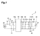
- FIG. 1 is a circuit diagram illustrating a schematic configuration of a switching circuit 1 according to one embodiment.
- FIG. 2 is a diagram for explaining a signal that drives the switching circuit 1.
- the switching circuit 1 is a switching power source circuit or a time-varying power source circuit, for example.
- the switching circuit 1 includes a switching element 10.
- the switching element 10 is an insulated field-effect transistor (MOSFET) unless otherwise noted.
- MOSFET insulated field-effect transistor
- Examples of the MOSFET include a power MOSFET.
- the switching element 10 has a source terminal 11 to be grounded, a gate terminal 12 connected to a signal source 20 and to which a signal is supplied from the signal source 20, and a drain terminal 13 connected to a power source section 30 and to which a voltage Vdd (e.g., 16 V) is supplied.
- Vdd e.g. 16 V
- An output parasitic capacitance C ds exists in the switching element 10 due to its configuration.
- the output parasitic capacitance C ds includes an output parasitic capacitance between a drain and a source. In FIG. 1 , the output parasitic capacitance C ds is shown as a capacitor 14.
- the signal source 20 supplies a signal for switching the switching element 10 to the gate terminal 12.
- the signal inputted into the gate terminal 12 from the signal source 20 is a PWM signal S P .
- the PWM signal S P will be described by reference to FIG. 2.
- FIG 2 is a diagram for explaining the PWM signal.
- FIG. 2(a) shows one example of two signals for generating the PWM signal S P .
- FIG 2(b) shows one example of the PWM signal.
- the PWM signal S P is a pulse signal whose duty cycle of a pulse width is modulated by a signal (S1) having a first frequency using a signal (S2) having a second frequency higher than the first frequency.
- Example of the signal (S2) is triangle-wave or sawtooth-wave signal (see FIG. 2(a) ).
- a clock frequency f CK of the PWM signal S P that is, a switching frequency that switches the switching element 10 corresponds to the second frequency.
- the other end of the signal source 20 is grounded.
- the power source section 30 is a direct-current power source section including a direct-current power source 31.
- the power source section 30 may include an inductor 32 in order to prevent the first frequency component of the switching element 10 from flowing into the direct-current power source 31.
- a positive pole of the direct-current power source 31 is connected to the drain terminal 13 via the inductor 32.
- a line connecting the drain terminal 13 and the direct-current power source 31 is referred to as signal path below.
- a negative pole of the direct-current power source 31 is grounded.
- a load circuit 40 is connected in parallel with the power source section 30.
- Examples of the load circuit 40 include a resistive load and an inductive load.
- One end 41 of the load circuit 40 is connected to the positive pole of the direct-current power source 31, and the other end 42 of the load circuit 40 is grounded.
- the inductor 32 when the inductor 32 is provided, the one end 41 of the load circuit 40 is connected to an end of the inductor 32 on the opposite side from the direct-current power source 31.
- the connection point functions as an output port P.
- the switching circuit 1 includes a passive circuit section 50 and a resonant circuit section 60 between the switching element 10 and the output port P so as to reduce power consumption in a switching operation.
- the passive circuit section 50 and the resonant circuit section 60 function as a filter that cuts an N-th order harmonic of the clock frequency f CK of the PWM signal S P and allows a frequency lower than the clock frequency f CK , i.e., the signal S1 having the first frequency to pass therethrough.
- the passive circuit section 50 and the resonant circuit section 60 will be described.
- the passive circuit section 50 is arranged between the switching element 10 and the output port P.
- the passive circuit section 50 has a first end 50a connected to the drain terminal 13, and a second end 50b connected to the output port P.
- the passive circuit section 50 has a configuration that satisfies next "passive circuit section conditions" at a frequency N times as high as the clock frequency f CK of the pulse signal supplied to the switching element 10.
- an impedance of the passive circuit section 50 anticipated from the switching element 10 (or as viewed from the switching element 10) is Z
- an imaginary part of the impedance Z is Z img .
- the imaginary part Z img of the impedance Z is zero or more, and twice or less of an absolute value of a reactance of the output parasitic capacitance C ds .
- the passive circuit section 50 may be a two-port circuit network composed of at least one reactance element.
- the passive circuit section 50 may be also a two-port circuit network composed of at least one transmission line (including a case of a stub). Specific examples of the passive circuit section 50 will be described later.
- the resonant circuit section 60 is a circuit that resonates at the frequency N times as high as the clock frequency f CK of the PWM signal S P as the pulse signal.
- a real part and an imaginary part of an impedance of the resonant circuit section 60 anticipated from the load circuit 40 (or as viewed from the load circuit 40) may be smaller than an impedance of the load circuit 40 at the frequency N times as high as the clock frequency f CK .
- FIG. 1 shows a circuit section obtained by connecting in parallel M resonant elements 61 1 to 61 M each having an inductor and a capacitor as a reactance element connected in series as one example.
- One end of each of the resonant elements 61 1 to 61 M is connected between the second end 50b and the output port P on the signal path connecting the output port P and the drain terminal 13.
- the other end of each of the resonant elements 61 1 to 61 M is grounded.
- An element value of each of the inductor and the capacitance of at least one resonant element out of the M resonant elements 61 1 to 61 M is an element value that allows resonance at the frequency N times as high as the clock frequency f CK .
- the extra power consumption is reduced in the switching circuit 1 including the passive circuit section 50 and the resonant circuit section 60 as described above. As a result, the power efficiency can be improved.
- the switching circuit 1 is sometimes referred to as switching circuit 1A.
- the passive circuit section 50 and the resonant circuit section 60 are referred to as passive circuit section 50A and resonant circuit section 60A, respectively.
- the passive circuit section 50A is a two-port circuit network composed of at least one reactance with no resistance.
- the resonant circuit section 60A is a parallel circuit composed of the M resonant elements 61 1 to 61 M as shown in FIG. 1 .
- the impedance Z of the passive circuit section 50A is composed only of the imaginary part.
- the passive circuit section 50A is designed such that the imaginary part Z img of the impedance Z satisfies the above "passive circuit section conditions.” That is, in the present embodiment, the passive circuit section 50A is designed such that the combined impedance of the passive circuit section 50A and the output parasitic capacitance C ds becomes infinity at the clock frequency f CK .
- the imaginary part Z img of the impedance of the passive circuit section 50 is equal to the absolute value of the reactance of the output parasitic capacitance C ds .
- the "passive circuit section conditions" are satisfied.
- the description is made by setting the reactance of the passive circuit section 50A with respect to the frequency of N times to X N ( ⁇ ) as a function of an angular frequency ⁇ .
- the passive circuit section 50A is described by exemplifying a specific numerical value for N, the same reference numerals may be assigned as the reference numerals of elements. Please note that element values of respective elements are set as numerical values corresponding to the exemplified value ofN.
- a horizontal axis represents an angular frequency ⁇
- a vertical axis represents a reactance ( ⁇ ).
- a solid line represents a reactance X 1 ( ⁇ ) of the passive circuit section 50A
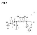
- the passive circuit section 50A having the reactance curve indicated in the expression (1) may be composed of an inductor 510 as one coil as shown in FIG. 4.
- the load circuit 40 is shown as a resistance.
- L 510 is an element value (an inductance) of the inductor 510.
- the resonant circuit section 60A may be composed of one inductor 62 and one capacitor 63 as shown in FIG. 4 .
- L 62 C 63 633.26 nH ⁇ pF from the expression (4).
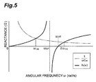
- a horizontal axis, a vertical axis, and an alternate long and short dash line are the same as those in FIG. 3 .
- a reactance X 2 ( ⁇ ) shown in FIG. 5 is expressed by an expression (5).
- [Expression 5] j ⁇ X 2 ⁇ j ⁇ a 2 j ⁇ 2 + ⁇ z ⁇ 1 2 j ⁇ 2 + ⁇ p ⁇ 1 2
- X 2 0 0 6 ⁇ a
- X 2 ⁇ CK 1 ⁇ CK ⁇ C ds 6 ⁇ b
- X 2 2 ⁇ ⁇ CK 1 2 ⁇ ⁇ CK ⁇ C ds 6 ⁇ c
- the circuit configuration is determined by executing topology search of the circuit configuration based on the expression (5).
- L 510 , C 520 , and L S11 are element values of the inductor 510, a capacitor 520, and an inductor 511 of the passive circuit section 50A.
- the element values L 510 , C 520 , and L 511 are provided by expressions (9a) to (9c) in the transformation process from the expression (7) to the expression (8).
- L 511 a 2 ⁇ ⁇ z ⁇ 1 2 - a 2 ⁇ ⁇ p ⁇ 1 2 ⁇ p ⁇ 1 2 9 ⁇ c
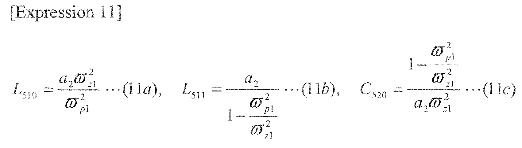
- L 510 , L 511 , and C 520 are provided by expressions (11a) to (11c) in the transformation process from the expression (7) to the expression (10).
- L 510 a 2 ⁇ ⁇ z ⁇ 1 2 ⁇ p ⁇ 1 2 11 ⁇ a
- L 511 a 2 1 - ⁇ p ⁇ 1 2 ⁇ z ⁇ 1 2 11 ⁇ b
- C 520 1 - ⁇ p ⁇ 1 2 ⁇ z ⁇ 1 2 a 2 ⁇ ⁇ z ⁇ 1 2 11 ⁇ c
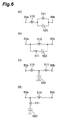
- the expressions (8) and (10) represent circuit configurations shown in FIGS. 6(a) and 6(b) . Since the resonant circuit section 60A resonates at the frequency once and twice as high as the clock frequency f CK , the second end 50b is shunted (that is, grounded) at the frequency. Therefore, a circuit configuration in FIG 6(c) is obtained as a modification of FIG. 6(a) , and a circuit in FIG. 6(d) is obtained as a modification of FIG. 6(b) .
- Element values of respective elements in circuits shown in FIGS. 6(a) and 6(b) can be calculated based on the expressions (9a) to (9c) and the expressions (11a) to (11c) by providing ⁇ z1 , ⁇ p1 , and a 2 so as to satisfy the expressions (6a) to (6c).
- the resonant circuit section 60 is composed of the two resonant elements 61 1 and 61 2 connected in parallel.
- the passive circuit section 50A may be composed of a combination of three inductors 510, 511, and 512 and two capacitors 520 and 521 (see FIGS.
- the passive circuit section 50A may be also composed of a combination of two inductors 510 and 511 and three capacitors 520, 521, and 522 (see FIGS. 7(l), 7(m), and 7(n) ).
- FIGS. 7(a) to 7(n) reference numerals are assigned for the sake of convenience so as to distinguish the inductors and the capacitors. Element values of the inductors and the capacitors of each circuit are set such that the inductors and the capacitors function as the passive circuit section 50A in the circuit.
- FIGS. 7(a) to 7(n) a terminal A and a terminal B are connected to the second end 50b or grounded.
- FIGS. 8(a) to 8(d) show configurations in which the terminals A and B in FIG. 7(a) are connected to the second end 50b or grounded.
- FIG. 8(a) shows a configuration in which both terminals A and B are grounded.
- FIG. 8(b) shows a configuration in which both terminals A and B are connected to the second terminal.
- FIG. 8(c) shows a configuration in which the terminal A is grounded and the terminal B is connected to the second terminal.
- FIG. 8(d) shows a configuration in which the terminal A is connected to the second terminal and the terminal B is grounded.
- the passive circuit section 50A capable of preventing a current having a frequency component of not only the harmonics of consecutive orders but of any two harmonics (e.g., the first-order and third-order harmonics) from flowing through the switching element 10 can be obtained.
- the circuit configurations shown in FIGS. 6(a) to 6(d) by adjusting the element values of the inductor elements and the capacitor elements, the passive circuit section 50A capable of preventing a current having a frequency component of not only the harmonics of consecutive orders but of any two harmonics (e.g., the first-order and third-order harmonics) from flowing through the switching element 10 can be obtained.
- the passive circuit section 50A capable of preventing a current having a frequency component of not only the harmonics of consecutive orders but of any three harmonics (e.g., the first-order harmonic, the third-order harmonic, and a fifth-order harmonic) from flowing through the switching element 10 can be obtained.
- the passive circuit section 50A and the resonant circuit section 60A are composed of the so-called lumped constant elements, higher efficiency can be achieved with smaller physical dimensions with respect to the same frequency as compared to a case in which the passive circuit section uses a distributed constant element when the clock frequency f CK is relatively low (e.g., 100 MHz or less).
- FIG. 9 is a schematic diagram illustrating a schematic configuration of a switching circuit including another example of a resonant circuit section.
- a switching circuit 1B may have the same configuration as that of the switching circuit 1 except for the configuration of a resonant circuit section 60B.
- the configuration of the resonant circuit section 60B will be mainly described.
- the resonant circuit section 60B has M end-open stubs of first to M-th end-open stubs 64 1 to 64 M whose one end is connected between the output port P and the second end 50b on the signal path.
- the first to M-th end-open stubs 64 1 to 64 M are so-called distributed constant elements.
- the first to M-th end-open stubs 64 1 to 64 M are transmission lines each having a predetermined impedance Z S and a predetermined electrical length.
- the electrical length of each of the first to M-th end-open stubs 64 1 to 64 M is determined according to a frequency at which each of the first to M-th end-open stubs 64 1 to 64 M resonates.
- the number M of lines may be determined regardless of a clock frequency or a harmonic order
- at least one of the first to M-th end-open stubs 64 1 to 64 M has an electrical length of 1/4 of a signal wavelength ⁇ with respect to the frequency N times as high as the clock frequency f CK .
- the electrical length of any end-open stub out of the M end-open stubs may be 1/4 of a signal wavelength ⁇ with respect to any harmonic.
- the first to M-th end-open stubs 64 1 to 64 M may be sometimes referred to as end-open stub 64 for the convenience of description.
- FIG 10 is a table showing that there are a plurality of harmonic orders at which one end-open stub can resonate at the same time.
- the second end-open stub 64 2 resonating at the second-order harmonic also resonates at sixth-order, tenth-order, fourteenth-order, ... , and (2k-1) x 2-th order harmonics at the same time.
- the M-th end-open stub 64 M resonating at a 2 M-1 -th order harmonic also resonates at 3 x 2 M-1 -th order, 5 x 2 M-1 -th order, 7 x 2 M-1 -th order, ..., and (2k-1) x 2 M-1 -th order harmonics at the same time.
- the number N of harmonic orders at which the end-open stub 64 resonates is indicated by a " ⁇ " mark in FIG. 10 . From FIG. 10 , when the first to M-th end-open stubs 64 1 to 64 M are provided in parallel, the consecutive number N of harmonic orders at which the end-open stub 64 can resonate is 2 M -1.
- n in FIG. 10 is an index number of the end-open stub 64 in the total number (M) of end-open stubs 64.
- the end-open stub 64 does not always need to resonate at harmonics of consecutive orders. For example, when harmonic components of even orders included in a switching voltage waveform are smaller than harmonic components of odd orders, it is effective to allow the end-open stub 64 to resonate at the harmonic components of odd orders. In this case, only one end-open stub 64 1 is required since the end-open stub 64 needs to resonate only at the harmonic components of odd orders.
- the first end-open stub 64 1 and the second end-open stub 64 2 are required.
- N 1, 2, 3, 4, 5, and 6, that is, up to the sixth-order harmonic of the clock frequency f CK .
- the first to third end-open stubs 64 1 , 64 2 , and 64 3 need to be connected in parallel.
- the harmonics of the plurality of orders N can be covered at the same time by one end-open stub 64 as described above since a standing wave formed in the end-open stub 64 has a periodic shape, and as a result, impedances as viewed from the point P toward the resonant circuit section 60B are the same (0 ⁇ ).
- each of the first to M-th end-open stubs 64 1 to 64 M is the so-called transmission line
- the first to M-th end-open stubs 64 1 to 64 M can be formed as a conductive pattern on a printed board. That is, the element can be formed without using separate components such as an inductor element and a capacitor element. Accordingly, when the resonant circuit section 60B is composed of the first to M-th end-open stubs 64 1 to 64 M as described in the second embodiment, the manufacturing efficiency, component cost, reliability and power durability of the switching circuit 1B can be improved.
- each of the first to M-th end-open stubs 64 1 to 64 M can be composed only of the transmission line, i.e., the conductive pattern on the printed board, its element value has high accuracy, so that the switching circuit 1B requires no adjustment after being manufactured.
- the passive circuit section 50A (50) is composed of the so-called lumped constant element.
- the passive circuit section 50 may be also composed of a distributed constant element.
- the passive circuit section 50 is referred to as passive circuit section 50B.
- the transmission line 530 may be a stub.
- the passive circuit section 50B is a two-port circuit network.
- An impedance matrix Z and an inverse matrix (an admittance matrix) Y are known for the two-port circuit network.
- the impedance matrix and the admittance matrix Y are expressed as in expressions (12a) and (12b) as a function of an angular frequency ⁇ .
- Z z 11 ⁇ z 12 ⁇ z 21 ⁇ z 22 ⁇
- a current having an angular frequency ⁇ 0, that is, a direct current needs to flow from the terminal 50a to the terminal 50b without a voltage drop.
- the terminal 50a when the terminal 50b is shunted to a ground terminal, the terminal 50a may be also regarded to be shunted. When expressed in an expression, this is expressed by an expression (13a).
- the direct current should not leak from the terminal 50a to the ground terminal.
- the terminal 50a when the terminal 50b is opened, the terminal 50a may be also regarded to be opened. This is expressed by an expression (13b).
- This is expressed by an expression (13c).
- y 11 0 ⁇ 13 ⁇ a
- z 11 0 ⁇ 13 ⁇ b
- y 11 ⁇ CK + j ⁇ ⁇ CK ⁇ C ds 0 13 ⁇ c
- a sign ⁇ has a meaning that an absolute value of a complex number becomes infinity.
- the required degree of freedom is 3 as indicated in the expressions (13a) to (13c).
- the expressions (13a) and (13b) are obtained at the same time when the transmission line 530 is one transmission line connected in series.
- the minimum required number of transmission lines is 1.
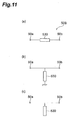
- the total number of topologies of the passive circuit section 50B composed of one transmission line 530 is 3 as shown in FIGS. 11 (a) to 11(c) .
- One that satisfies at least one of an incompatibility condition (I) and an incompatibility condition (II) described below is eliminated from the above three topologies.
- the reason why the circuit satisfying the incompatibility condition (II) is incompatible as the circuit of the passive circuit section 50B is that the second end 50b corresponds to be grounded at the clock frequency f CK , so that the voltage of the clock frequency f CK is not applied to the transmission line 530 in the configuration of the incompatibility condition (II) and there is not enough degree of freedom.
- an electrical length of the transmission line 530 is determined.
- the electrical length of the transmission line 530 can be represented by a phase difference ⁇ 530 at the clock frequency f CK .
- the electrical length is also referred to as electrical length ⁇ 530 below.
- Z 0 is a characteristic impedance of the transmission line 530.
- the passive circuit section 50B is designed so as to satisfy the following four conditions by re-using an element of the admittance matrix Y indicated in the expression (12b).
- the required degree of freedom is 4 as indicated in the expressions (16a) to (16d).
- the minimum number of transmission lines 530 of the passive circuit section 50B is 2.
- the two transmission lines 530 are separately described, the two transmission lines 530 are referred to as transmission lines 531 and 532.
- the total number of topologies of the passive circuit section 50B composed of the two transmission lines (including the case of the stub) is 10 as shown in FIGS. 12(a) to 12(j) .
- the incompatibility conditions (I) and (II) By eliminating one that satisfies at least one of the incompatibility conditions (I) and (II) from the 10 topologies, configurations shown in FIGS. 12(a) to 12(c) remain.
- the characteristic impedance of the transmission line 531 is referred to as Z 531 , and the electrical length of the transmission line 531 is referred to as ⁇ 531 .
- the characteristic impedance of the transmission line 532 is referred to as Z 532 , and the electrical length of the transmission line 532 is referred to as ⁇ 532 .
- a next expression is obtained.
- the clock frequency f CK is 200 MHz.
- ⁇ CK 2 ⁇ x 200 MHz.
- C ds 60 pF.
- the respective transmission lines 531 and 532 can be configured.
- the resonant circuit section 60 resonated at the clock frequency f CK and the frequency twice as high as the clock frequency f CK , that is, the second end 50b was shunted (grounded).
- a signal having a frequency f (MHz) was supplied to the first end 50a from the signal source 20.
- FIG. 14 is a graph showing a simulation result.
- a horizontal axis represents the frequency f CK supplied to the first end
- a vertical axis represents an admittance.
- a solid line represents a real part of the combined admittance of the passive circuit section 50B and the output parasitic capacitance C ds
- a dash line represents an imaginary part of the combined admittance.
- FIG. 15 it can be understood that the real part and the imaginary part of the combined admittance become zero when the frequency f CK is 200 MHz, and 400 MHz as the frequency twice as high as 200 MHz, and the expressions (16c) and (16d) are satisfied. It can be also understood that the imaginary part of the combined admittance becomes infinity when the frequency is 0, and the expression (16a) is also satisfied.
- the transmission line 530 is a conductive pattern on a printed board
- the element can be easily formed without using separate components such as an inductor and a capacitor.
- the manufacturing efficiency, component cost, reliability and power durability of a switching circuit 1C can be improved in a similar manner to the second embodiment.
- the passive circuit section 50B can be formed only by the transmission line, i.e., the conductive pattern on the printed board, the switching circuit 1C requires no adjustment after being manufactured because of the same reason as that in the second embodiment.
- the passive circuit section 50B capable of preventing the current having the frequency component up to the N-th order harmonic (that is, the first-order to N-th order harmonics) with N as a maximum order out of the harmonics of consecutive orders of the clock frequency f CK from flowing through the switching element 10 has been described.
- the element values of the passive circuit section 50 are determined on the condition that the combined impedance of the passive circuit section 50 and the output parasitic capacitance C ds becomes infinity at the frequency N times as high as the clock frequency f CK (or the combined admittance becomes zero at the frequency N times as high as the clock frequency f CK ).
- any element value may be employed for the elements of the passive circuit section 50 as long as the passive circuit section 50 satisfies the above "passive circuit section conditions.” The same applies to the resonant circuit section 60.
- the elements constituting the resonant circuit section 60 are designed such that the real part and the imaginary part of the impedance of the resonant circuit section 60 become zero at the frequency N times as high as the clock frequency f CK .
- the real part and the imaginary part of the impedance of the resonant circuit section 60 may not necessarily become zero in actual circuit manufacturing. That is, the element values of the elements constituting the resonant circuit section 60 may be any value as long as the real part and the imaginary part of the impedance of the resonant circuit section 60 are smaller than the impedance of the load circuit 40 in a resonant state.
- the passive circuit section 50 and the resonant circuit section 60 in the various embodiments described above may be combined together.
- the switching circuit may include the passive circuit section composed of the lumped constant element and the resonant circuit section composed of the distributed constant element.
- the switching circuit may include the passive circuit section composed of the distributed constant element and the resonant circuit section composed of the lumped constant element.
- the switching element may be a field-effect transistor other than the insulated field-effect transistor, a bipolar transistor, and an insulated gate transistor in addition to the insulated field-effect transistor.
- the signal that drives the switching element is the PWM signal, any pulse signal may be employed as long as the ON/OFF switching of the switching element can be controlled.
- the resonant circuit section 60B is composed of the end-open stub 64.
- the resonant circuit section 60B may be composed of the transmission line as the distributed constant element.
Landscapes
- Engineering & Computer Science (AREA)
- Power Engineering (AREA)
- Electronic Switches (AREA)
- Amplifiers (AREA)
- Dc-Dc Converters (AREA)
Abstract
Description
- The present invention relates to a switching circuit.
- There are known switching circuits using switching elements such as transistors (See Patent Literature 1). In the switching circuit disclosed in
Patent Literature 1, a PWM (pulse width modulation) signal is supplied to an input terminal (e.g., a gate terminal) of the switching element. The switching element is controlled to be switched ON/OFF by a clock frequency (a switching frequency) of the PWM signal. A voltage at a connection point between an output terminal (e.g., a drain terminal) and an inductor varies by the switching ON/OFF of the switching element. As a result, driving of a load circuit whose one end is connected to the connection point can be controlled. - [Patent Literature 1] Japanese Patent Laid-Open No.
2006-101637 - However, an extra current may flow through the load circuit or the switching element due to a signal component that is an integer multiple of the clock frequency (the switching frequency) for switching ON/OFF the switching element in addition to a current flowing through the load circuit when the switching element is in an ON state. Thus, there is unnecessary power consumption.
- It is an object of the present invention to provide a switching circuit which can improve power efficiency.
- A switching circuit according to one aspect of the present invention includes: a switching element that has a first terminal and a second terminal, and is driven by a pulse signal to switch a conduction state between the first terminal and the second terminal; a power source section that supplies a voltage to the first terminal of the switching element; a load circuit that is connected in parallel with the power source section; a passive circuit section that is connected between a connection point between the power source section and the load circuit, and the first terminal of the switching element, and suppresses a current flowing from the connection point to the switching element at a frequency N times (N is an integer of 1 or more) as high as a clock frequency of the pulse signal; and a resonant circuit section that is connected between the passive circuit section and the connection point, and resonates at the frequency of N times.
- In the configuration, the switching element is connected to the connection point via the passive circuit section and the resonant circuit section. Thus, the state of a voltage supplied to the connection point from the power source section can be controlled by a switching operation of the switching element. As a result, the state of a voltage applied to the load circuit connected in parallel with the power source section can be controlled. Meanwhile, the passive circuit section suppresses the current flowing from the connection point to the switching element at the frequency N times as high as the clock frequency of the pulse signal. Thus, extra energy consumption can be reduced. Furthermore, the resonant circuit section resonates at the frequency of N times. Thus, the N-time frequency component out of the voltage component applied to the load circuit is reduced, so that extra energy consumption can be reduced. As a result, power efficiency can be improved.
- In one embodiment, an imaginary part of an impedance of the passive circuit section anticipated from the switching element may be zero or more, and twice or less of an absolute value of a reactance of an output parasitic capacitance of the switching element. In this case, the imaginary part of the impedance of the passive circuit section anticipated from the switching element may be zero or more, and twice or less of the absolute value of the reactance of the output parasitic capacitance of the switching element at the frequency of N times.
- In the embodiment, the passive circuit section can more reliably suppress the current flowing from the connection point to the switching element at the frequency N times as high as the clock frequency of the pulse signal.
- In one embodiment, a real part and an imaginary part of an impedance of the resonant circuit section anticipated from the load circuit may be smaller than an impedance of the load circuit at the clock frequency of N times.
- In the embodiment, the voltage applied to the load circuit can be further reduced at the frequency of N times. As a result, extra energy consumption can be reduced.
- The pulse signal may be a signal obtained by temporally modulating a duty cycle of a pulse width of the pulse signal by a signal having a lower frequency component than the clock frequency.
- While the passive circuit section and the resonant circuit section act against the frequency N times as high as the clock frequency, the passive circuit section and the resonant circuit section do not substantially act against the lower frequency component than the clock frequency. Thus, the signal having the lower frequency component can easily pass through the passive circuit section and the resonant circuit section to be transmitted to the load circuit. As a result, the state of the voltage applied to the load circuit varies by the signal component.
- In one embodiment, the passive circuit section may be composed of at least one reactance element, and may have a first end connected to the first terminal of the switching element and a second end connected to the connection point.
- In one embodiment, the passive circuit section may be composed of at least one transmission line, and may have a first end connected to the first terminal of the switching element and a second end connected to the connection point.
- In one embodiment, the resonant circuit section may have M resonant elements each having at least one reactance element connected in series. In the embodiment, at least one resonant element out of the M resonant elements may resonate at the frequency of N times. The M resonant elements may be connected in parallel.
- In one embodiment, the resonant circuit section may have M (M is an integer of 1 or more) transmission lines. In the embodiment, at least one transmission line out of the M transmission lines may have an electrical length of 1/4 of a wavelength corresponding to the frequency N times as high as the clock frequency.
- The present invention can provide the switching circuit which can improve the power efficiency.
-
- [
Fig. 1] FIG. 1 is a diagram illustrating a schematic configuration of a switching circuit according to one embodiment. - [
Fig. 2] FIG. 2 is a diagram for explaining a signal that drives the switching circuit shown inFIG. 1 . - [
Fig. 3] FIG. 3 is a diagram showing design conditions of a passive circuit section having the minimum number of elements and designed with respect to a clock frequency. - [
Fig. 4] FIG. 4 is a diagram illustrating one example of a configuration of the switching circuit operating at the clock frequency; - [
Fig. 5] FIG. 5 is a diagram showing design conditions of a passive circuit section having the minimum number of elements out of passive circuit sections designed with respect to first-order and second-order harmonics of the clock frequency. - [
Fig. 6] FIG. 6 is a diagram illustrating examples of a circuit configuration of the passive circuit section designed with respect to the first-order and second-order harmonics of the clock frequency; - [
Fig. 7] FIG. 7 is a diagram illustrating examples of a circuit configuration of a passive circuit section designed with respect to the first-order harmonic, the second-order harmonic, and a third-order harmonic of the clock frequency; - [
Fig. 8] FIG. 8 is a diagram illustrating specific examples of a connection state of terminals A and B in the circuit configuration shown inFIG. 7(a) . - [
Fig. 9] FIG. 9 is a schematic diagram illustrating a schematic configuration of a switching circuit including another example of a resonant circuit section. - [
Fig. 10] FIG. 10 is a table showing that there are a plurality of harmonic orders at which one end-open stub can resonate at the same time. - [
Fig. 11] FIG. 11 is a diagram illustrating arrangement options of a transmission line when a passive circuit section is composed of one transmission line. - [
Fig. 12] FIG. 12 is a diagram illustrating arrangement options of transmission lines when the passive circuit section is composed of two transmission lines. - [
Fig. 13] FIG. 13 is a diagram illustrating a circuit for simulations when the passive circuit section is composed of two transmission lines. - [
Fig. 14] FIG. 14 is a diagram showing a simulation result. - [
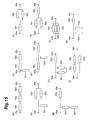
Fig. 15] FIG 15 is a diagram illustrating configuration examples of the passive circuit section composed of three transmission lines. - In the following, embodiments of the present invention will be described by reference to the drawings. In the description of the drawings, the same elements are assigned the same reference numerals to omit the overlapping description. The dimensional ratios in the drawings do not necessarily correspond to those of the description.
- A switching circuit according to one embodiment will be described based on
FIGS. 1 and2 .FIG. 1 is a circuit diagram illustrating a schematic configuration of aswitching circuit 1 according to one embodiment.FIG. 2 is a diagram for explaining a signal that drives theswitching circuit 1. Theswitching circuit 1 is a switching power source circuit or a time-varying power source circuit, for example. - The
switching circuit 1 includes a switchingelement 10. In the present embodiment, the switchingelement 10 is an insulated field-effect transistor (MOSFET) unless otherwise noted. Examples of the MOSFET include a power MOSFET. In this case, the switchingelement 10 has asource terminal 11 to be grounded, agate terminal 12 connected to asignal source 20 and to which a signal is supplied from thesignal source 20, and adrain terminal 13 connected to apower source section 30 and to which a voltage Vdd (e.g., 16 V) is supplied. An output parasitic capacitance Cds exists in the switchingelement 10 due to its configuration. The output parasitic capacitance Cds includes an output parasitic capacitance between a drain and a source. InFIG. 1 , the output parasitic capacitance Cds is shown as acapacitor 14. - The
signal source 20 supplies a signal for switching the switchingelement 10 to thegate terminal 12. The signal inputted into thegate terminal 12 from thesignal source 20 is a PWM signal SP. The PWM signal SP will be described by reference toFIG. 2. FIG 2 is a diagram for explaining the PWM signal.FIG. 2(a) shows one example of two signals for generating the PWM signal SP.FIG 2(b) shows one example of the PWM signal. The PWM signal SP is a pulse signal whose duty cycle of a pulse width is modulated by a signal (S1) having a first frequency using a signal (S2) having a second frequency higher than the first frequency. Example of the signal (S2) is triangle-wave or sawtooth-wave signal (seeFIG. 2(a) ). A clock frequency fCK of the PWM signal SP, that is, a switching frequency that switches the switchingelement 10 corresponds to the second frequency. The other end of thesignal source 20 is grounded. - Returning to
FIG. 1 , the configuration of theswitching circuit 1 will be described. Thepower source section 30 is a direct-current power source section including a direct-current power source 31. Thepower source section 30 may include aninductor 32 in order to prevent the first frequency component of the switchingelement 10 from flowing into the direct-current power source 31. A positive pole of the direct-current power source 31 is connected to thedrain terminal 13 via theinductor 32. A line connecting thedrain terminal 13 and the direct-current power source 31 is referred to as signal path below. A negative pole of the direct-current power source 31 is grounded. - A
load circuit 40 is connected in parallel with thepower source section 30. Examples of theload circuit 40 include a resistive load and an inductive load. Oneend 41 of theload circuit 40 is connected to the positive pole of the direct-current power source 31, and theother end 42 of theload circuit 40 is grounded. As shown inFIG. 1 , when theinductor 32 is provided, the oneend 41 of theload circuit 40 is connected to an end of theinductor 32 on the opposite side from the direct-current power source 31. The connection point functions as an output port P. - In the above configuration, when the PWM signal SP supplied from the
signal source 20 is inputted into the switchingelement 10, a conduction state between thedrain terminal 13 and thesource terminal 11 is switched by the PWM signal SP. The state of a voltage at the output port P thereby varies, so that the state of a voltage applied to theload circuit 40 changes. As a result, a current flowing through theload circuit 40 varies. Accordingly, for example, when a high-frequency power amplifier is connected as the load circuit, an output amplitude of a high-frequency signal can be modulated with a large depth while high power efficiency is being maintained for the power source. - The
switching circuit 1 includes apassive circuit section 50 and aresonant circuit section 60 between the switchingelement 10 and the output port P so as to reduce power consumption in a switching operation. Thepassive circuit section 50 and theresonant circuit section 60 function as a filter that cuts an N-th order harmonic of the clock frequency fCK of the PWM signal SP and allows a frequency lower than the clock frequency fCK, i.e., the signal S1 having the first frequency to pass therethrough. In the following, thepassive circuit section 50 and theresonant circuit section 60 will be described. - The
passive circuit section 50 is arranged between the switchingelement 10 and the output port P. Thepassive circuit section 50 has afirst end 50a connected to thedrain terminal 13, and asecond end 50b connected to the output port P. Thepassive circuit section 50 has a configuration that satisfies next "passive circuit section conditions" at a frequency N times as high as the clock frequency fCK of the pulse signal supplied to the switchingelement 10. In the following description, an impedance of thepassive circuit section 50 anticipated from the switching element 10 (or as viewed from the switching element 10) is Z, and an imaginary part of the impedance Z is Zimg. - The imaginary part Zimg of the impedance Z is zero or more, and twice or less of an absolute value of a reactance of the output parasitic capacitance Cds.
- When the above "passive circuit section conditions" are satisfied, a combined impedance of the output parasitic capacitance Cds and the
passive circuit section 50 becomes large at the N-th order harmonic. As a result, thepassive circuit section 50 prevents a current having the N-time clock frequency component from flowing through the switchingelement 10. Thus, extra power consumed in the switchingelement 10 in the switching operation can be reduced. As long as thepassive circuit section 50 is configured to satisfy the "passive circuit section conditions", thepassive circuit section 50 may be a two-port circuit network composed of at least one reactance element. Thepassive circuit section 50 may be also a two-port circuit network composed of at least one transmission line (including a case of a stub). Specific examples of thepassive circuit section 50 will be described later. - The
resonant circuit section 60 is a circuit that resonates at the frequency N times as high as the clock frequency fCK of the PWM signal SP as the pulse signal. As an example of a resonant state, a real part and an imaginary part of an impedance of theresonant circuit section 60 anticipated from the load circuit 40 (or as viewed from the load circuit 40) may be smaller than an impedance of theload circuit 40 at the frequency N times as high as the clock frequency fCK. -
FIG. 1 shows a circuit section obtained by connecting in parallel Mresonant elements 611 to 61M each having an inductor and a capacitor as a reactance element connected in series as one example. One end of each of theresonant elements 611 to 61M is connected between thesecond end 50b and the output port P on the signal path connecting the output port P and thedrain terminal 13. The other end of each of theresonant elements 611 to 61M is grounded. An element value of each of the inductor and the capacitance of at least one resonant element out of the Mresonant elements 611 to 61M is an element value that allows resonance at the frequency N times as high as the clock frequency fCK. - In the configuration, when the switching
element 10 performs the switching operation at the frequency N times as high as the clock frequency fCK, resonance occurs in theresonant circuit section 60. Due to the resonance, the real part and the imaginary part of the impedance of theresonant circuit section 60 become smaller than the impedance of theload circuit 40. Thus, a current flows through theresonant circuit section 60 more easily than through theload circuit 40. That is, when the switchingelement 10 performs the switching operation, the frequency component N times as high as the clock frequency fCK, which the voltage applied to theload circuit 40 may have, approaches zero. Accordingly, extra energy consumption by theload circuit 40 can be reduced at the N-th order harmonic of the clock frequency fCK. - The extra power consumption is reduced in the
switching circuit 1 including thepassive circuit section 50 and theresonant circuit section 60 as described above. As a result, the power efficiency can be improved. - In the following, the configurations of the
passive circuit section 50 and theresonant circuit section 60 will be specifically described by reference to various embodiments. - In the embodiment, the switching
circuit 1 is sometimes referred to as switchingcircuit 1A. Thepassive circuit section 50 and theresonant circuit section 60 are referred to aspassive circuit section 50A andresonant circuit section 60A, respectively. Thepassive circuit section 50A is a two-port circuit network composed of at least one reactance with no resistance. Theresonant circuit section 60A is a parallel circuit composed of the Mresonant elements 611 to 61M as shown inFIG. 1 . - In this case, the impedance Z of the
passive circuit section 50A is composed only of the imaginary part. Thepassive circuit section 50A is designed such that the imaginary part Zimg of the impedance Z satisfies the above "passive circuit section conditions." That is, in the present embodiment, thepassive circuit section 50A is designed such that the combined impedance of thepassive circuit section 50A and the output parasitic capacitance Cds becomes infinity at the clock frequency fCK. In this case, the imaginary part Zimg of the impedance of thepassive circuit section 50 is equal to the absolute value of the reactance of the output parasitic capacitance Cds. Thus, the "passive circuit section conditions" are satisfied. In the following, the description is made by setting the reactance of thepassive circuit section 50A with respect to the frequency of N times to XN(ω) as a function of an angular frequency ω. Although thepassive circuit section 50A is described by exemplifying a specific numerical value for N, the same reference numerals may be assigned as the reference numerals of elements. Please note that element values of respective elements are set as numerical values corresponding to the exemplified value ofN. - First, a case of N = 1 will be described. Although N and M do not necessarily correspond to each other, N = 1 and M = 1 in the following description.
FIG. 3 is a graph showing design conditions of the passive circuit section having the minimum number of elements in the case of N = 1. InFIG. 3 , a horizontal axis represents an angular frequency ω, and a vertical axis represents a reactance (Ω). InFIG. 3 , a solid line represents a reactance X1(ω) of thepassive circuit section 50A, and an alternate long and short dash line is a reactance curve of the output parasitic capacitance Cds based on the absolute value of the reactance of the output parasitic capacitance Cds. Since the reactance X1(ω) shown inFIG 3 is a linear function, the reactance X1(ω) is expressed by a following expression.
[Expression 1]
- The
passive circuit section 50A having the reactance curve indicated in the expression (1) may be composed of aninductor 510 as one coil as shown inFIG. 4. FIG. 4 is a diagram illustrating one example of the configuration of the switching circuit in the case of N = 1. Theload circuit 40 is shown as a resistance. In the expression (1), L510 is an element value (an inductance) of theinductor 510. When an angular frequency corresponding to the clock frequency fCK is ωCK, conditions to be satisfied by theinductor 510 as thepassive circuit section 50A are as follows.
[Expression 2]

- An expression (3) is obtained from the expressions (2a) and (2b).
[Expression 3]
- When the clock frequency fCK is 200 MHz, ωCK = 2π x 200 MHz. Moreover, when Cds = 60 pF, L510 = 10.54 nH.
- Here, one example of a method for calculating element values of elements constituting the
resonant circuit section 60A will be described. In the case of M = 1 and N = 1, theresonant circuit section 60A may be composed of oneinductor 62 and onecapacitor 63 as shown inFIG. 4 . Resonant conditions of theresonant element 611 are expressed by a next expression.
[Expression 4]
- When a resistance value RL of the
load circuit 40 is 10 Ω, Cds = 60 pF, and ωCK = 2π x 200 MHz, L62C63 = 633.26 nH·pF from the expression (4). Element values L62 and C63 of theinductor 62 and thecapacitor 63 may be determined so as to satisfy L62C63 = 633.26 nH·pF. - Next, a case of N = 2 will be described. Here, the
passive circuit section 50A capable of preventing a current having a frequency component up to a second-order harmonic (specifically, a fundamental wave and the second-order harmonic) out of harmonics of consecutive orders from the fundamental wave (the case of N = 1) from flowing through the switchingelement 10 will be described. In this case, while N and M do not necessarily correspond to each other as described above, theresonant circuit section 60A also needs to resonate at a frequency once and twice as high as the clock frequency fCK. Thus, N = 2 and M = 2.FIG. 5 is a graph showing design conditions of the passive circuit section having the minimum number of elements in the case of N = 2. InFIG 5 , a horizontal axis, a vertical axis, and an alternate long and short dash line are the same as those inFIG. 3 . - A reactance X2(ω) shown in
FIG. 5 is expressed by an expression (5).
[Expression 5]
- In the expression (5), ωz1 is an angular frequency that satisfies X2(ω) = 0, and a first angular frequency from a direct current (ω = 0), ωp1 is an angular frequency of a first pole from the direct current (that is, ω = 0), and a2 is a free parameter determined so as to satisfy expressions (6a) to (6c) as the design conditions of the
passive circuit section 50A.

- The
passive circuit section 50A may be designed as described below in the case of N = 2. First, the circuit configuration is determined by executing topology search of the circuit configuration based on the expression (5). - For example, when jω=s in the expression (5), the expression (5) is expressed by an expression (7).
[Expression 7]
- An expression (8) is obtained by transforming the expression (7).
[Expression 8]
- In the expression (8), L510, C520, and LS11 are element values of the
inductor 510, acapacitor 520, and aninductor 511 of thepassive circuit section 50A. The element values L510, C520, and L511 are provided by expressions (9a) to (9c) in the transformation process from the expression (7) to the expression (8).
- The expression (7) can be also transformed into an expression (10).
[Expression 10]
- In the expression (10), L510, L511, and C520 are provided by expressions (11a) to (11c) in the transformation process from the expression (7) to the expression (10).
- The expressions (8) and (10) represent circuit configurations shown in
FIGS. 6(a) and 6(b) . Since theresonant circuit section 60A resonates at the frequency once and twice as high as the clock frequency fCK, thesecond end 50b is shunted (that is, grounded) at the frequency. Therefore, a circuit configuration inFIG 6(c) is obtained as a modification ofFIG. 6(a) , and a circuit inFIG. 6(d) is obtained as a modification ofFIG. 6(b) . - Element values of respective elements in circuits shown in
FIGS. 6(a) and 6(b) can be calculated based on the expressions (9a) to (9c) and the expressions (11a) to (11c) by providing ωz1, ωp1, and a2 so as to satisfy the expressions (6a) to (6c). In the case of N = 2 and M = 2, theresonant circuit section 60 is composed of the tworesonant elements resonant elements - In a case of N = 3, the
passive circuit section 50A can be also designed in a similar manner to the case of N = 2. Here, thepassive circuit section 50A capable of preventing a current having a frequency component up to a third-order harmonic (specifically, the fundamental wave, the second-order harmonic, and the third-order harmonic) out of the harmonics of consecutive orders from the fundamental wave (the case of N = 1) from flowing through the switchingelement 10 will be described.FIGS. 7(a) to 7(n) are diagrams illustrating configuration examples of thepassive circuit section 50A in the case of N = 3. In the case of N = 3, thepassive circuit section 50A may be composed of a combination of threeinductors capacitors 520 and 521 (seeFIGS. 7(a) to 7(k) ). In the case of N = 3, thepassive circuit section 50A may be also composed of a combination of twoinductors capacitors FIGS. 7(l), 7(m), and 7(n) ). InFIGS. 7(a) to 7(n) , reference numerals are assigned for the sake of convenience so as to distinguish the inductors and the capacitors. Element values of the inductors and the capacitors of each circuit are set such that the inductors and the capacitors function as thepassive circuit section 50A in the circuit. - In
FIGS. 7(a) to 7(n) , a terminal A and a terminal B are connected to thesecond end 50b or grounded. The case of a circuit configuration inFIG. 7(a) will be specifically described as one example.FIGS. 8(a) to 8(d) show configurations in which the terminals A and B inFIG. 7(a) are connected to thesecond end 50b or grounded. -
FIG. 8(a) shows a configuration in which both terminals A and B are grounded.FIG. 8(b) shows a configuration in which both terminals A and B are connected to the second terminal.FIG. 8(c) shows a configuration in which the terminal A is grounded and the terminal B is connected to the second terminal.FIG. 8(d) shows a configuration in which the terminal A is connected to the second terminal and the terminal B is grounded. Although the configuration inFIG. 7(a) has been specifically described, the same applies toFIGS. 7(b) to 7(n) . Accordingly, in the case of N = 3, thepassive circuit section 50A may have 38 circuit configurations. - In the case of N = 3, the
resonant circuit section 60A is composed of the threeresonant elements 611 to 613 connected in parallel as M = 3. Element values of the inductor and the capacitor constituting each of theresonant elements 611 to 613 can be calculated in a similar manner to the case of N = 1. - Here, the configuration of the
passive circuit section 50A capable of preventing a current having a frequency component up to the N-th order harmonic (that is, the first-order to N-th order harmonics) with the exemplified N as a maximum order from flowing through the switchingelement 10 has been mainly described with respect to each of the cases of N = 1 to 3. Even when N is 4 or more, thepassive circuit section 50A can also similarly prevent the current having the frequency component up to the N-th order harmonic with N as a maximum order from flowing through the switchingelement 10. When N is 4 or more, element values of the inductor and the capacitor constituting each of theresonant elements 614 to 61M of theresonant circuit section 60A can be also calculated in a similar manner to the cases of N = 1, 2, and 3. Please note that N and M do not necessarily correspond to each other as described above. - In the circuit configurations shown in
FIGS. 6(a) to 6(d) , by adjusting the element values of the inductor elements and the capacitor elements, thepassive circuit section 50A capable of preventing a current having a frequency component of not only the harmonics of consecutive orders but of any two harmonics (e.g., the first-order and third-order harmonics) from flowing through the switchingelement 10 can be obtained. Similarly, in the circuit configurations shown inFIGS. 7(a) to 7(n) , by adjusting the element values of the inductor elements and the capacitor elements, thepassive circuit section 50A capable of preventing a current having a frequency component of not only the harmonics of consecutive orders but of any three harmonics (e.g., the first-order harmonic, the third-order harmonic, and a fifth-order harmonic) from flowing through the switchingelement 10 can be obtained. - As described above, when the
passive circuit section 50A and theresonant circuit section 60A are composed of the so-called lumped constant elements, higher efficiency can be achieved with smaller physical dimensions with respect to the same frequency as compared to a case in which the passive circuit section uses a distributed constant element when the clock frequency fCK is relatively low (e.g., 100 MHz or less). -
FIG. 9 is a schematic diagram illustrating a schematic configuration of a switching circuit including another example of a resonant circuit section. A switchingcircuit 1B may have the same configuration as that of theswitching circuit 1 except for the configuration of aresonant circuit section 60B. Thus, the configuration of theresonant circuit section 60B will be mainly described. - The
resonant circuit section 60B has M end-open stubs of first to M-th end-open stubs 641 to 64M whose one end is connected between the output port P and thesecond end 50b on the signal path. The first to M-th end-open stubs 641 to 64M are so-called distributed constant elements. In other words, the first to M-th end-open stubs 641 to 64M are transmission lines each having a predetermined impedance ZS and a predetermined electrical length. The electrical length of each of the first to M-th end-open stubs 641 to 64M is determined according to a frequency at which each of the first to M-th end-open stubs 641 to 64M resonates. While the number M of lines may be determined regardless of a clock frequency or a harmonic order, at least one of the first to M-th end-open stubs 641 to 64M has an electrical length of 1/4 of a signal wavelength λ with respect to the frequency N times as high as the clock frequency fCK. In this case, the electrical length of any end-open stub out of the M end-open stubs may be 1/4 of a signal wavelength λ with respect to any harmonic. In the following description, the first to M-th end-open stubs 641 to 64M may be sometimes referred to as end-open stub 64 for the convenience of description. -
FIG 10 is a table showing that there are a plurality of harmonic orders at which one end-open stub can resonate at the same time. For example, the first end-open stub 641 resonating at the fundamental wave (the first-order harmonic) in the case of N = 1 also resonates at third-order, fifth-order, seventh-order, ..., and (2k-1)-th order harmonics at the same time in addition to the first-order harmonic (k is an integer of 1 or more). Similarly, the second end-open stub 642 resonating at the second-order harmonic also resonates at sixth-order, tenth-order, fourteenth-order, ... , and (2k-1) x 2-th order harmonics at the same time. The M-th end-open stub 64M resonating at a 2M-1-th order harmonic also resonates at 3 x 2M-1-th order, 5 x 2M-1-th order, 7 x 2M-1-th order, ..., and (2k-1) x 2M-1-th order harmonics at the same time. The number N of harmonic orders at which the end-open stub 64 resonates is indicated by a "○" mark inFIG. 10 . FromFIG. 10 , when the first to M-th end-open stubs 641 to 64M are provided in parallel, the consecutive number N of harmonic orders at which the end-open stub 64 can resonate is 2M-1.FIG. 10 shows a combination in which the end-open stub 64 continuously resonates through N = 1 to 15 by using n = 1 to 4 as one example. However, the combination of n and N is not limited thereto. "n" inFIG. 10 is an index number of the end-open stub 64 in the total number (M) of end-open stubs 64. The end-open stub 64 does not always need to resonate at harmonics of consecutive orders. For example, when harmonic components of even orders included in a switching voltage waveform are smaller than harmonic components of odd orders, it is effective to allow the end-open stub 64 to resonate at the harmonic components of odd orders. In this case, only one end-open stub 641 is required since the end-open stub 64 needs to resonate only at the harmonic components of odd orders. - The points above will be specifically described. To allow the
resonant circuit section 60B to continuously resonate through, for example, N = 1, 2, and 3, that is, up to the third-order harmonic, the first end-open stub 641 and the second end-open stub 642 are required. To allow theresonant circuit section 60B to continuously resonate through N = 1, 2, 3, 4, 5, and 6, that is, up to the sixth-order harmonic of the clock frequency fCK, the first to third end-open stubs 641, 642, and 643 need to be connected in parallel. The harmonics of the plurality of orders N can be covered at the same time by one end-open stub 64 as described above since a standing wave formed in the end-open stub 64 has a periodic shape, and as a result, impedances as viewed from the point P toward theresonant circuit section 60B are the same (0 Ω). - Since each of the first to M-th end-open stubs 641 to 64M is the so-called transmission line, the first to M-th end-open stubs 641 to 64M can be formed as a conductive pattern on a printed board. That is, the element can be formed without using separate components such as an inductor element and a capacitor element. Accordingly, when the
resonant circuit section 60B is composed of the first to M-th end-open stubs 641 to 64M as described in the second embodiment, the manufacturing efficiency, component cost, reliability and power durability of theswitching circuit 1B can be improved. Since each of the first to M-th end-open stubs 641 to 64M can be composed only of the transmission line, i.e., the conductive pattern on the printed board, its element value has high accuracy, so that theswitching circuit 1B requires no adjustment after being manufactured. - In the first embodiment, the
passive circuit section 50A (50) is composed of the so-called lumped constant element. However, thepassive circuit section 50 may be also composed of a distributed constant element. The case in which thepassive circuit section 50 is composed of the distributed constant element will be described. Here, thepassive circuit section 50 is referred to aspassive circuit section 50B. - The
passive circuit section 50B including atransmission line 530 as the distributed constant element may be designed as described below. First, the case of N = 1 will be described. In one embodiment, thetransmission line 530 may be a stub. - The
passive circuit section 50B is a two-port circuit network. An impedance matrix Z and an inverse matrix (an admittance matrix) Y are known for the two-port circuit network. The impedance matrix and the admittance matrix Y are expressed as in expressions (12a) and (12b) as a function of an angular frequency ω.
[Expression 12]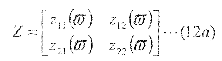

- A current having an angular frequency ω = 0, that is, a direct current needs to flow from the terminal 50a to the terminal 50b without a voltage drop. To satisfy the condition, when the terminal 50b is shunted to a ground terminal, the terminal 50a may be also regarded to be shunted. When expressed in an expression, this is expressed by an expression (13a). Moreover, the direct current should not leak from the terminal 50a to the ground terminal. To satisfy the condition, when the terminal 50b is opened, the terminal 50a may be also regarded to be opened. This is expressed by an expression (13b). Furthermore, a current having an angular frequency ω = ωCK, that is, a current having the clock frequency is prevented from flowing from the
drain terminal 12 toward thepassive circuit section 50B (the right side inFIG. 1 ). That is, a parallel combined admittance of the terminal 50a and the output parasitic capacitance Cds may become zero when the terminal 50b is shunted to the ground. This is expressed by an expression (13c).
- In the expressions (13a) and (13b), a sign ∞ has a meaning that an absolute value of a complex number becomes infinity.
- In the case of N = 1, the required degree of freedom is 3 as indicated in the expressions (13a) to (13c). However, the expressions (13a) and (13b) are obtained at the same time when the
transmission line 530 is one transmission line connected in series. Thus, the minimum required number of transmission lines is 1. - The total number of topologies of the
passive circuit section 50B composed of onetransmission line 530 is 3 as shown inFIGS. 11 (a) to 11(c) . One that satisfies at least one of an incompatibility condition (I) and an incompatibility condition (II) described below is eliminated from the above three topologies. - Incompatibility condition (I): The end is grounded with respect to the direct current.
- Incompatibility condition (II): An element that directly shunts the
second end 50b is provided. - The reason why the circuit satisfying the incompatibility condition (I) is incompatible as the circuit of the
passive circuit section 50B is that the circuit satisfying the incompatibility condition (I) contradicts the expression (13b). The reason why the circuit satisfying the incompatibility condition (II) is incompatible as the circuit of thepassive circuit section 50B is that thesecond end 50b corresponds to be grounded at the clock frequency fCK, so that the voltage of the clock frequency fCK is not applied to thetransmission line 530 in the configuration of the incompatibility condition (II) and there is not enough degree of freedom. - When the inappropriate topology is eliminated by applying the incompatibility condition (I) and the incompatibility condition (II) to the three types of topologies, the
passive circuit section 50B composed of the distributed constant element has a configuration shown inFIG 11(a) in the case of N = 1. - By applying such a condition that a combined impedance Zc1 of the output parasitic capacitance Cds and the
passive circuit section 50B becomes infinity at the clock frequency fCK, that is, the expression (13c) to thepassive circuit section 50B shown inFIG. 11(a) in a similar manner to the first embodiment, an electrical length of thetransmission line 530 is determined. The electrical length of thetransmission line 530 can be represented by a phase difference θ530 at the clock frequency fCK. Thus, the electrical length is also referred to as electrical length θ530 below. - To be more specific, the expression (13c) as the condition that the combined impedance Zc1 of the output parasitic capacitance Cds and the
passive circuit section 50B becomes infinity at the clock frequency fCK (or that the combined admittance becomes zero at the clock frequency fCK) is expressed by an expression (14).
[Expression 14]
- In the expression (14), Z0 is a characteristic impedance of the
transmission line 530. An expression (15) is obtained from the expression (14).
[Expression 15]
- For example, when Cds = 60 pF, ωCK = 2π x 200 MHz, and Z0 = 50 Ω, θ530 = 0.2593 radians. Thus, when the clock frequency fCK is 200 MHz and the output parasitic capacitance Cds is 60 pF, the
transmission line 530 in the case of N = 1 may be configured such that the impedance Z0 is 50 Ω and the electrical length (the phase difference) is 0.2593 radians. - In the case of N = 2, the
passive circuit section 50B is designed so as to satisfy the following four conditions by re-using an element of the admittance matrix Y indicated in the expression (12b). Here, thepassive circuit section 50B capable of preventing the current having the frequency component up to the second-order harmonic (that is, the fundamental wave (the case of N = 1) and the second-order harmonic) out of the harmonics of consecutive orders of the clock frequency fCK from flowing through the switchingelement 10 will be described as thepassive circuit section 50B in the case of N = 2.
- It is the same as the case of the expressions (13a) and (13c) that y11(ω) in the expressions (16a), (16c), and (16d) is a first element of the admittance matrix Y.
- In the case of the
passive circuit section 50B corresponding to up to the second-order harmonic, the required degree of freedom is 4 as indicated in the expressions (16a) to (16d). Thus, the minimum number oftransmission lines 530 of thepassive circuit section 50B is 2. When the twotransmission lines 530 are separately described, the twotransmission lines 530 are referred to astransmission lines - The total number of topologies of the
passive circuit section 50B composed of the two transmission lines (including the case of the stub) is 10 as shown inFIGS. 12(a) to 12(j) . By eliminating one that satisfies at least one of the incompatibility conditions (I) and (II) from the 10 topologies, configurations shown inFIGS. 12(a) to 12(c) remain. - By applying the conditions of the expressions (16c) and (16d), that is, the condition that the combined admittance becomes zero at the fundamental wave (N = 1) and the second-order harmonic (N = 2) at the same time, the characteristic impedance and the electrical length of each of the
transmission lines - The case in
FIG. 12(a) will be specifically described. The characteristic impedance of thetransmission line 531 is referred to as Z531, and the electrical length of thetransmission line 531 is referred to as θ531. Similarly, the characteristic impedance of thetransmission line 532 is referred to as Z532, and the electrical length of thetransmission line 532 is referred to as θ532. In this case, a next expression is obtained.
[Expression 17]

- When Z531/Z532 = α, a next expression is obtained from the above expressions.
[Expression 18]
- From the expressions (17a), (17b), and (18), Z531 and Z532 are expressed as below.
[Expression 19]

- Here, the clock frequency fCK is 200 MHz. In this case, ωCK = 2π x 200 MHz. Also, it is assumed that Cds = 60 pF. One example of a solution obtained when the expressions (19a) and (19b) are numerically calculated is as follows.
- Z531 = 60.0347 Ω
- θ531 = 27°
- Z532 = 21.4348 Ω
- θ532 = 144°
- Since the characteristic impedances Z531 and Z532 and the electrical lengths θ531 and θ532 of the
respective transmission lines respective transmission lines - A simulation was performed using a circuit configuration shown in
FIG 13 by providing Z531, θ531, Z532, and θ532 described above. In the circuit configuration shown inFIG. 13 , it was assumed that theresonant circuit section 60 resonated at the clock frequency fCK and the frequency twice as high as the clock frequency fCK, that is, thesecond end 50b was shunted (grounded). A signal having a frequency f (MHz) was supplied to thefirst end 50a from thesignal source 20. -
FIG. 14 is a graph showing a simulation result. InFIG. 14 , a horizontal axis represents the frequency fCK supplied to the first end, and a vertical axis represents an admittance. InFIG 14 , a solid line represents a real part of the combined admittance of thepassive circuit section 50B and the output parasitic capacitance Cds, and a dash line represents an imaginary part of the combined admittance. As shown inFIG. 15 , it can be understood that the real part and the imaginary part of the combined admittance become zero when the frequency fCK is 200 MHz, and 400 MHz as the frequency twice as high as 200 MHz, and the expressions (16c) and (16d) are satisfied. It can be also understood that the imaginary part of the combined admittance becomes infinity when the frequency is 0, and the expression (16a) is also satisfied. - In the case of N = 3 or more, the
passive circuit section 50B may be similarly composed of the distributed constant elements. For example,FIGS. 15(a) to 15(k) are diagrams illustrating configuration examples of thepassive circuit section 50B capable of preventing the current having the frequency component up to the third-order harmonic (that is, the fundamental wave (the case of N = 1), the second-order harmonic, and the third-order harmonic) out of the harmonics of consecutive orders of the clock frequency fCK from flowing through the switchingelement 10 as thepassive circuit section 50B in the case of N = 3. InFIGS. 15(a) to 15(k) , threetransmission lines 530 are referred to astransmission lines respective transmission lines 530 can be determined in a similar manner to the case of N = 2. - Since the
transmission line 530 is a conductive pattern on a printed board, the element can be easily formed without using separate components such as an inductor and a capacitor. As a result, the manufacturing efficiency, component cost, reliability and power durability of a switching circuit 1C can be improved in a similar manner to the second embodiment. Since thepassive circuit section 50B can be formed only by the transmission line, i.e., the conductive pattern on the printed board, the switching circuit 1C requires no adjustment after being manufactured because of the same reason as that in the second embodiment. - Here, the
passive circuit section 50B capable of preventing the current having the frequency component up to the N-th order harmonic (that is, the first-order to N-th order harmonics) with N as a maximum order out of the harmonics of consecutive orders of the clock frequency fCK from flowing through the switchingelement 10 has been described. However, as long as thepassive circuit section 50B is designed with respect to the N-th order harmonic, thepassive circuit section 50B may be designed so as to prevent a current having a frequency component of harmonics of any one or more orders (e.g., odd or even orders) up to the N-th order harmonic from the fundamental wave (the case of N = 1) from flowing through the switchingelement 10, for example. - In the various embodiments of the
passive circuit section 50 described above, the element values of thepassive circuit section 50 are determined on the condition that the combined impedance of thepassive circuit section 50 and the output parasitic capacitance Cds becomes infinity at the frequency N times as high as the clock frequency fCK (or the combined admittance becomes zero at the frequency N times as high as the clock frequency fCK). However, any element value may be employed for the elements of thepassive circuit section 50 as long as thepassive circuit section 50 satisfies the above "passive circuit section conditions." The same applies to theresonant circuit section 60. That is, in the various embodiments of theresonant circuit section 60, the elements constituting theresonant circuit section 60 are designed such that the real part and the imaginary part of the impedance of theresonant circuit section 60 become zero at the frequency N times as high as the clock frequency fCK. However, the real part and the imaginary part of the impedance of theresonant circuit section 60 may not necessarily become zero in actual circuit manufacturing. That is, the element values of the elements constituting theresonant circuit section 60 may be any value as long as the real part and the imaginary part of the impedance of theresonant circuit section 60 are smaller than the impedance of theload circuit 40 in a resonant state. - Moreover, the
passive circuit section 50 and theresonant circuit section 60 in the various embodiments described above may be combined together. For example, in addition to the case in which both of the passive circuit section and the resonant circuit section are composed of the lumped constant elements or the distributed constant elements, the switching circuit may include the passive circuit section composed of the lumped constant element and the resonant circuit section composed of the distributed constant element. Conversely, the switching circuit may include the passive circuit section composed of the distributed constant element and the resonant circuit section composed of the lumped constant element. - Although the embodiments of the present invention have been described above, the present invention is not limited to the aforementioned various embodiments, and various modifications may be made therein without departing from the scope of the present invention. For example, the switching element may be a field-effect transistor other than the insulated field-effect transistor, a bipolar transistor, and an insulated gate transistor in addition to the insulated field-effect transistor. Although the signal that drives the switching element is the PWM signal, any pulse signal may be employed as long as the ON/OFF switching of the switching element can be controlled. Moreover, in the second embodiment, the
resonant circuit section 60B is composed of the end-open stub 64. However, theresonant circuit section 60B may be composed of the transmission line as the distributed constant element. - 1, 1A, 1B... switching circuit; 10... switching element; 11...source terminal (second terminal); 13...drain terminal(first terminal); 14... capacitor; 30...DC power source section (power source section); 40...load circuit; 41...one end; 42...the other end; 50, 50A, 50B...passive circuit section; 50a...first terminal(first terminal of passive circuit section); 50b...second terminal(second terminal of passive circuit section); 60, 60A, 60B...resonant circuit section; 611to 61N...resonant element; 641to 64n...end-open stub; 530, 531, 532, 533...transmission line; P...output port(connection point)
Claims (8)
- A switching circuit comprising:a switching element that has a first terminal and a second terminal, and is driven by a pulse signal to switch a conduction state between the first terminal and the second terminal;a power source section that supplies a voltage to the first terminal of the switching element;a load circuit that is connected in parallel with the power source section;a passive circuit section that is connected between a connection point between the power source section and the load circuit, and the first terminal of the switching element, and suppresses a current flowing from the connection point to the switching element at a frequency N times (N is an integer of 1 or more) as high as a clock frequency of the pulse signal; anda resonant circuit section that is connected between the passive circuit section and the connection point, and resonates at the frequency of N times.
- The switching circuit according to claim 1,
wherein an imaginary part of an impedance of the passive circuit section anticipated from the switching element is greater than zero, and twice or less of an absolute value of a reactance of an output parasitic capacitance of the switching element. - The switching circuit according to claim 1 or 2,
wherein a real part and an imaginary part of an impedance of the resonant circuit section anticipated from the load circuit are smaller than an impedance of the load circuit at the clock frequency of N times. - The switching circuit according to any one of claims 1 to 3,
wherein the pulse signal is a signal obtained by temporally modulating a duty cycle of a pulse width of the pulse signal by a signal having a lower frequency component than the clock frequency. - The switching circuit according to any one of claims 1 to 4,
wherein the passive circuit section is composed of at least one reactance element, and has a first end connected to the first terminal of the switching element and a second end connected to the connection point. - The switching circuit according to any one of claims 1 to 4,
wherein the passive circuit section is composed of at least one transmission line, and has a first end connected to the first terminal of the switching element and a second end connected to the connection point. - The switching circuit according to any one of claims 1 to 6,
wherein the resonant circuit section has M (M is an integer of 1 or more) resonant elements each having at least one reactance element connected in series, and
at least one resonant element out of the M resonant elements resonates at the frequency N times as high as the clock frequency. - The switching circuit according to any one of claims 1 to 6,
wherein the resonant circuit section has M (M is an integer of 1 or more) transmission lines, and
at least one transmission line out of the M transmission lines has an electrical length of 1/4 of a wavelength corresponding to the frequency N times as high as the clock frequency.
Applications Claiming Priority (2)
| Application Number | Priority Date | Filing Date | Title |
|---|---|---|---|
| JP2011141988A JP5759286B2 (en) | 2011-06-27 | 2011-06-27 | Switching circuit |
| PCT/JP2012/058995 WO2013001882A1 (en) | 2011-06-27 | 2012-04-02 | Switching circuit |
Publications (2)
| Publication Number | Publication Date |
|---|---|
| EP2725708A1 true EP2725708A1 (en) | 2014-04-30 |
| EP2725708A4 EP2725708A4 (en) | 2014-04-30 |
Family
ID=47361286
Family Applications (1)
| Application Number | Title | Priority Date | Filing Date |
|---|---|---|---|
| EP12805194.3A Withdrawn EP2725708A4 (en) | 2011-06-27 | 2012-04-02 | SWITCHING CIRCUIT |
Country Status (6)
| Country | Link |
|---|---|
| US (1) | US8536930B2 (en) |
| EP (1) | EP2725708A4 (en) |
| JP (1) | JP5759286B2 (en) |
| CN (1) | CN103548258B (en) |
| TW (1) | TWI525988B (en) |
| WO (1) | WO2013001882A1 (en) |
Cited By (1)
| Publication number | Priority date | Publication date | Assignee | Title |
|---|---|---|---|---|
| WO2016201896A1 (en) * | 2015-06-16 | 2016-12-22 | 深圳市华讯方舟科技有限公司 | Equivalent inductive circuit of e-class power amplifier and device parameter acquisition method |
Families Citing this family (6)
| Publication number | Priority date | Publication date | Assignee | Title |
|---|---|---|---|---|
| JP5727561B2 (en) * | 2013-08-29 | 2015-06-03 | 住友電気工業株式会社 | Transformer |
| JP2017093175A (en) * | 2015-11-11 | 2017-05-25 | 株式会社ダイヘン | High frequency power supply device and non-contact power transmission system |
| US9929704B2 (en) * | 2015-12-14 | 2018-03-27 | Qualcomm Incorporated | Class E2 amplifier |
| ITUA20161824A1 (en) * | 2016-03-18 | 2017-09-18 | Eggtronic S R L | CIRCUIT AND METHOD TO DRIVE ELECTRIC LOADS |
| JP6708003B2 (en) * | 2016-06-16 | 2020-06-10 | 株式会社オートネットワーク技術研究所 | Power supply control device |
| US11431334B2 (en) * | 2020-04-06 | 2022-08-30 | Analog Devices International Unlimited Company | Closed loop switch control system and method |
Family Cites Families (13)
| Publication number | Priority date | Publication date | Assignee | Title |
|---|---|---|---|---|
| JPH0644696B2 (en) * | 1984-07-30 | 1994-06-08 | 富士通テン株式会社 | Pulse width modulation power amplifier demodulation filter |
| JPH09266421A (en) * | 1996-03-28 | 1997-10-07 | Kokusai Electric Co Ltd | High frequency power amplifier |
| US6924681B2 (en) * | 2001-05-23 | 2005-08-02 | Texas Instruments Incorporated | Efficient pulse amplitude modulation transmit modulation |
| DE10252146B4 (en) * | 2002-11-09 | 2012-03-29 | Hüttinger Elektronik Gmbh + Co. Kg | Method for generating a high-frequency alternating voltage and high-frequency power amplifier therefor |
| JP4467395B2 (en) | 2004-09-29 | 2010-05-26 | ローム株式会社 | Power supply |
| US7345539B2 (en) * | 2005-02-10 | 2008-03-18 | Raytheon Company | Broadband microwave amplifier |
| TWI260953B (en) * | 2005-05-19 | 2006-08-21 | Ligtek Electronics Co Ltd | Constant power control circuit device and control method thereof |
| US7719336B2 (en) * | 2006-10-31 | 2010-05-18 | Andrew Roman Gizara | Pulse width modulation sequence maintaining maximally flat voltage during current transients |
| JP2010141522A (en) * | 2008-12-10 | 2010-06-24 | Sony Corp | Amplifier and communication apparatus |
| JP5408616B2 (en) * | 2009-08-31 | 2014-02-05 | 国立大学法人電気通信大学 | Amplifier circuit |
| CN102906998A (en) * | 2010-05-27 | 2013-01-30 | 京瓷株式会社 | Amplification circuit, communication device, and transmission device using amplification circuit |
| US8749995B2 (en) * | 2011-03-29 | 2014-06-10 | Texas Instruments Incorporated | Single-pulse resonant gate driver for driving switches in resonant isolated converters and other systems |
| JP5580782B2 (en) * | 2011-06-06 | 2014-08-27 | 住友電気工業株式会社 | Switching circuit |
-
2011
- 2011-06-27 JP JP2011141988A patent/JP5759286B2/en not_active Expired - Fee Related
-
2012
- 2012-04-02 WO PCT/JP2012/058995 patent/WO2013001882A1/en not_active Ceased
- 2012-04-02 CN CN201280024953.0A patent/CN103548258B/en not_active Expired - Fee Related
- 2012-04-02 EP EP12805194.3A patent/EP2725708A4/en not_active Withdrawn
- 2012-05-10 TW TW101116713A patent/TWI525988B/en not_active IP Right Cessation
- 2012-06-27 US US13/535,001 patent/US8536930B2/en not_active Expired - Fee Related
Non-Patent Citations (3)
| Title |
|---|
| Andrei Grebennikov: "A High-Efficiency Transmission-Line GaN HEMT Class E Power Amplifier", High Frequency Electronics, 1 January 2009 (2009-01-01), pages 16-24, XP055107317, Retrieved from the Internet: URL:http://www.highfrequencyelectronics.com/Archives/Dec09/HFE1209_Grebennikov.pdf [retrieved on 2014-03-12] * |
| Frederick H Raab: "HIGH-EFFICIENCY RF POWER AMPLIFIERS AND TRANSMITTERS", , 1 January 2009 (2009-01-01), XP055106636, Retrieved from the Internet: URL:http://projectx-docdb.fnal.gov/cgi-bin/RetrieveFile?docid=853;filename=RaabHEPA.pdf;version=1 [retrieved on 2014-03-10] * |
| See also references of WO2013001882A1 * |
Cited By (1)
| Publication number | Priority date | Publication date | Assignee | Title |
|---|---|---|---|---|
| WO2016201896A1 (en) * | 2015-06-16 | 2016-12-22 | 深圳市华讯方舟科技有限公司 | Equivalent inductive circuit of e-class power amplifier and device parameter acquisition method |
Also Published As
| Publication number | Publication date |
|---|---|
| US20120326774A1 (en) | 2012-12-27 |
| WO2013001882A1 (en) | 2013-01-03 |
| US8536930B2 (en) | 2013-09-17 |
| JP5759286B2 (en) | 2015-08-05 |
| JP2013009260A (en) | 2013-01-10 |
| CN103548258A (en) | 2014-01-29 |
| TW201320596A (en) | 2013-05-16 |
| EP2725708A4 (en) | 2014-04-30 |
| TWI525988B (en) | 2016-03-11 |
| CN103548258B (en) | 2016-09-07 |
Similar Documents
| Publication | Publication Date | Title |
|---|---|---|
| EP2725708A1 (en) | Switching circuit | |
| JP5711354B2 (en) | Class characteristic variable amplifier | |
| CN102006019B (en) | Amplifier circuit | |
| JP6643972B2 (en) | Bus bar structure and power conversion device using the same | |
| EP2128979A1 (en) | Variable frequency band removing filter | |
| KR20090097162A (en) | Pulse amplifier | |
| US20120049834A1 (en) | Circuit and method to suppress the parasitic resonance from a dc/dc converter | |
| JP7165355B2 (en) | power amplifier circuit | |
| US10644613B2 (en) | Inverter for inductive power transfer | |
| Hosotani et al. | A novel analysis of ZVS wireless power transfer system using coupled resonators | |
| JP6816661B2 (en) | FET drive circuit | |
| US9548706B2 (en) | High-frequency generator | |
| US20200304108A1 (en) | Electronic driver circuit for at least one power mosfet and method operating at least one power mosfet | |
| JP2007194871A (en) | Harmonic oscillator using transmission line type resonator | |
| JP5822660B2 (en) | High frequency switch | |
| KR101283746B1 (en) | Rf oscillator | |
| Huang et al. | Investigation and design of coupler structure in capacitive wireless power transfer with free-positioning feature | |
| US11196384B2 (en) | Power amplifier | |
| US20090302932A1 (en) | Feeding Arrangement for an Ultrasonic Device | |
| Ikutajima et al. | Choke-less Class-E Oscillator Using p-MOSFET and n-MOSFET | |
| JP6661190B2 (en) | Variable reactance circuit | |
| Miyahara et al. | Design of class-E M power amplifier with one input signal | |
| US10505098B2 (en) | Drive signal generating apparatus | |
| Sarkar et al. | Mathematical Analysis of Duty Cycle Variation based Wireless Power Control Technique | |
| CN102428760A (en) | Resonant power converters for driving inductive loads such as discharge lamps |
Legal Events
| Date | Code | Title | Description |
|---|---|---|---|
| PUAI | Public reference made under article 153(3) epc to a published international application that has entered the european phase |
Free format text: ORIGINAL CODE: 0009012 |
|
| 17P | Request for examination filed |
Effective date: 20131129 |
|
| A4 | Supplementary search report drawn up and despatched |
Effective date: 20140325 |
|
| AK | Designated contracting states |
Kind code of ref document: A1 Designated state(s): AL AT BE BG CH CY CZ DE DK EE ES FI FR GB GR HR HU IE IS IT LI LT LU LV MC MK MT NL NO PL PT RO RS SE SI SK SM TR |
|
| RIN1 | Information on inventor provided before grant (corrected) |
Inventor name: ISHIOKA KAZUYA Inventor name: OHIRA TAKASHI Inventor name: SHIGA NOBUO Inventor name: WADA KAZUYUKI Inventor name: SAWADA KAZUSHI Inventor name: WUREN TUYA Inventor name: HATSUKAWA SATOSHI Inventor name: FUJIKAWA KAZUHIRO |
|
| DAX | Request for extension of the european patent (deleted) | ||
| STAA | Information on the status of an ep patent application or granted ep patent |
Free format text: STATUS: EXAMINATION IS IN PROGRESS |
|
| 17Q | First examination report despatched |
Effective date: 20170301 |
|
| STAA | Information on the status of an ep patent application or granted ep patent |
Free format text: STATUS: THE APPLICATION IS DEEMED TO BE WITHDRAWN |
|
| 18D | Application deemed to be withdrawn |
Effective date: 20170712 |