EP2725649A1 - Stacked cell and method for manufacturing same - Google Patents
Stacked cell and method for manufacturing same Download PDFInfo
- Publication number
- EP2725649A1 EP2725649A1 EP12802743.0A EP12802743A EP2725649A1 EP 2725649 A1 EP2725649 A1 EP 2725649A1 EP 12802743 A EP12802743 A EP 12802743A EP 2725649 A1 EP2725649 A1 EP 2725649A1
- Authority
- EP
- European Patent Office
- Prior art keywords
- electrode
- positive
- positive electrode
- separator
- bonded
- Prior art date
- Legal status (The legal status is an assumption and is not a legal conclusion. Google has not performed a legal analysis and makes no representation as to the accuracy of the status listed.)
- Granted
Links
Images









Classifications
-
- H—ELECTRICITY
- H01—ELECTRIC ELEMENTS
- H01M—PROCESSES OR MEANS, e.g. BATTERIES, FOR THE DIRECT CONVERSION OF CHEMICAL ENERGY INTO ELECTRICAL ENERGY
- H01M50/00—Constructional details or processes of manufacture of the non-active parts of electrochemical cells other than fuel cells, e.g. hybrid cells
- H01M50/40—Separators; Membranes; Diaphragms; Spacing elements inside cells
- H01M50/46—Separators, membranes or diaphragms characterised by their combination with electrodes
-
- H—ELECTRICITY
- H01—ELECTRIC ELEMENTS
- H01M—PROCESSES OR MEANS, e.g. BATTERIES, FOR THE DIRECT CONVERSION OF CHEMICAL ENERGY INTO ELECTRICAL ENERGY
- H01M10/00—Secondary cells; Manufacture thereof
- H01M10/04—Construction or manufacture in general
- H01M10/0413—Large-sized flat cells or batteries for motive or stationary systems with plate-like electrodes
-
- H—ELECTRICITY
- H01—ELECTRIC ELEMENTS
- H01M—PROCESSES OR MEANS, e.g. BATTERIES, FOR THE DIRECT CONVERSION OF CHEMICAL ENERGY INTO ELECTRICAL ENERGY
- H01M10/00—Secondary cells; Manufacture thereof
- H01M10/04—Construction or manufacture in general
- H01M10/0436—Small-sized flat cells or batteries for portable equipment
-
- H—ELECTRICITY
- H01—ELECTRIC ELEMENTS
- H01M—PROCESSES OR MEANS, e.g. BATTERIES, FOR THE DIRECT CONVERSION OF CHEMICAL ENERGY INTO ELECTRICAL ENERGY
- H01M10/00—Secondary cells; Manufacture thereof
- H01M10/05—Accumulators with non-aqueous electrolyte
- H01M10/052—Li-accumulators
-
- H—ELECTRICITY
- H01—ELECTRIC ELEMENTS
- H01M—PROCESSES OR MEANS, e.g. BATTERIES, FOR THE DIRECT CONVERSION OF CHEMICAL ENERGY INTO ELECTRICAL ENERGY
- H01M10/00—Secondary cells; Manufacture thereof
- H01M10/05—Accumulators with non-aqueous electrolyte
- H01M10/058—Construction or manufacture
- H01M10/0585—Construction or manufacture of accumulators having only flat construction elements, i.e. flat positive electrodes, flat negative electrodes and flat separators
-
- H—ELECTRICITY
- H01—ELECTRIC ELEMENTS
- H01M—PROCESSES OR MEANS, e.g. BATTERIES, FOR THE DIRECT CONVERSION OF CHEMICAL ENERGY INTO ELECTRICAL ENERGY
- H01M50/00—Constructional details or processes of manufacture of the non-active parts of electrochemical cells other than fuel cells, e.g. hybrid cells
- H01M50/40—Separators; Membranes; Diaphragms; Spacing elements inside cells
- H01M50/409—Separators, membranes or diaphragms characterised by the material
-
- H—ELECTRICITY
- H01—ELECTRIC ELEMENTS
- H01M—PROCESSES OR MEANS, e.g. BATTERIES, FOR THE DIRECT CONVERSION OF CHEMICAL ENERGY INTO ELECTRICAL ENERGY
- H01M50/00—Constructional details or processes of manufacture of the non-active parts of electrochemical cells other than fuel cells, e.g. hybrid cells
- H01M50/40—Separators; Membranes; Diaphragms; Spacing elements inside cells
- H01M50/409—Separators, membranes or diaphragms characterised by the material
- H01M50/411—Organic material
- H01M50/414—Synthetic resins, e.g. thermoplastics or thermosetting resins
-
- Y—GENERAL TAGGING OF NEW TECHNOLOGICAL DEVELOPMENTS; GENERAL TAGGING OF CROSS-SECTIONAL TECHNOLOGIES SPANNING OVER SEVERAL SECTIONS OF THE IPC; TECHNICAL SUBJECTS COVERED BY FORMER USPC CROSS-REFERENCE ART COLLECTIONS [XRACs] AND DIGESTS
- Y02—TECHNOLOGIES OR APPLICATIONS FOR MITIGATION OR ADAPTATION AGAINST CLIMATE CHANGE
- Y02E—REDUCTION OF GREENHOUSE GAS [GHG] EMISSIONS, RELATED TO ENERGY GENERATION, TRANSMISSION OR DISTRIBUTION
- Y02E60/00—Enabling technologies; Technologies with a potential or indirect contribution to GHG emissions mitigation
- Y02E60/10—Energy storage using batteries
-
- Y—GENERAL TAGGING OF NEW TECHNOLOGICAL DEVELOPMENTS; GENERAL TAGGING OF CROSS-SECTIONAL TECHNOLOGIES SPANNING OVER SEVERAL SECTIONS OF THE IPC; TECHNICAL SUBJECTS COVERED BY FORMER USPC CROSS-REFERENCE ART COLLECTIONS [XRACs] AND DIGESTS
- Y02—TECHNOLOGIES OR APPLICATIONS FOR MITIGATION OR ADAPTATION AGAINST CLIMATE CHANGE
- Y02P—CLIMATE CHANGE MITIGATION TECHNOLOGIES IN THE PRODUCTION OR PROCESSING OF GOODS
- Y02P70/00—Climate change mitigation technologies in the production process for final industrial or consumer products
- Y02P70/50—Manufacturing or production processes characterised by the final manufactured product
-
- Y—GENERAL TAGGING OF NEW TECHNOLOGICAL DEVELOPMENTS; GENERAL TAGGING OF CROSS-SECTIONAL TECHNOLOGIES SPANNING OVER SEVERAL SECTIONS OF THE IPC; TECHNICAL SUBJECTS COVERED BY FORMER USPC CROSS-REFERENCE ART COLLECTIONS [XRACs] AND DIGESTS
- Y10—TECHNICAL SUBJECTS COVERED BY FORMER USPC
- Y10T—TECHNICAL SUBJECTS COVERED BY FORMER US CLASSIFICATION
- Y10T156/00—Adhesive bonding and miscellaneous chemical manufacture
- Y10T156/10—Methods of surface bonding and/or assembly therefor
Definitions
- the present invention relates to a laminated cell and a method for manufacturing the same.
- a laminated cell has a laminated body formed by sequentially stacking a positive electrode, a separator, a negative electrode, and a separator. Misalignment in stacking may cause short circuit, reduction of the cell capacity due to reduction in the effective power generation area, and other defects. Thus, the misalignment in stacking is conventionally suppressed by disposing the positive electrode in a bag-shaped separator (see Patent Literature 1, for example).
- Patent Literature 1 Japanese Patent Application Publication No. Hei 7-302616
- the conventional technique has a problem that the number of work steps is large and improvement in productivity is difficult. Moreover, since the thermal fusion bonding may cause the thickness of the bag-shaped separator to decrease and thereby cause defects such as holes, a certain interval needs to be secured between an outer peripheral portion of the positive electrode and the thermal fusion bonding portion. Accordingly, the conventional technique has a problem that size reduction of the cell through size reduction of the bag-shaped separator is difficult to achieve.
- An object of the present invention is to provide a laminated cell which has excellent productivity and which can be easily reduced in size, and a manufacturing method for the same.
- a laminated cell in a first aspect of the present invention includes a laminated body formed by sequentially stacking a negative electrode, a separator, a positive electrode, and a separator. At least one of surfaces of the positive electrode or the negative electrode in a stacking direction has a portion to which a resin member is bonded, and the separators each has a portion bonded to the resin member on a side facing the at least one of surfaces.
- a method for manufacturing a laminated cell having a laminated body formed by sequentially stacking a negative electrode, a separator, a positive electrode, and a separator in a second aspect of the present invention includes the step of bonding a portion of each of the separators on a side facing at least one of surfaces of the positive electrode or the negative electrode in a stacking direction to a resin member bonded to a portion in the at least one of surfaces.
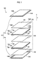
- Fig. 1 is an exploded perspective view for explaining a laminated cell in a first embodiment
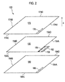
- Fig. 2 is an exploded perspective view for explaining a sub-assembly shown in Fig. 1
- Figs. 3 and 4 are cross-sectional views respectively for explaining a front portion and a rear portion of the sub-assembly shown in Fig. 1 .
- a laminated cell 100 in the first embodiment is formed of, for example, a substantially-rectangular lithium-ion secondary cell and has an exterior member 110 and a laminated body 120 forming a cell main body.
- the exterior member 110 is formed of an upper portion 112 and a lower portion 114 and is used to prevent shock from the outside and deterioration due to an environment. Outer peripheral portions of sheet members forming the upper portion 112 and the lower portion 114 are partially or entirely bonded to each other by thermal fusion bonding. From the view point of weight reduction and thermal conductivity, the sheet members in the exterior member 110 are preferably made of polymer-metal composite laminated film in which a metal is covered with an insulator such as a polypropylene film. A metal such as aluminum, stainless steel, nickel, or copper or an alloy of these metals can be used as the metal in the sheet members. Note that reference numerals 114A and 114B respectively denote a front edge portion and a rear edge portion of the exterior member 110.
- the laminated body 120 is formed by sequentially stacking negative electrodes 130 and sub-assemblies 122.
- the sub-assemblies 122 each have a positive electrode 150 and separators 170, 180.
- the separators 170, 180 are disposed respectively on both sides of the positive electrode 150 in a stacking direction S.
- the number of the stacked negative electrodes 130 and the stacked sub-assemblies 122 is determined as appropriate in consideration of the required capacity and the like.
- each negative electrode 130 has a substantially-rectangular shape and has a negative-electrode current collector 140 and negative-electrode active material layers 145.
- the negative-electrode current collector 140 is formed of a high-conductivity member and has a negative-electrode current collecting portion 132 for taking out generated electric power to the outside.
- the negative-electrode active material layers 145 are regions in which a negative-electrode active material is disposed, the negative-electrode active material being a material to which lithium is inserted and from which lithium is extracted.
- the negative-electrode active material layers 145 are disposed on both surfaces of the negative-electrode current collector 140 except for the negative-electrode current collecting portion 132 and are in contact with the negative-electrode current collector 140.
- An outer peripheral portion of the negative electrode 130 is formed of: a front edge portion 134A in which the negative-electrode current collecting portion 132 is disposed; a rear edge portion 134B which is opposite to the front edge portion; and side edge portions 134C, 134D which are opposite to each other and which connect the front edge portion 134A and the rear edge portion 134B to each other.
- each positive electrode 150 has a substantially-rectangular shape and has a positive-electrode current collector 160 and positive-electrode active material layers 165.
- the positive-electrode current collector 160 is formed of a high-conductivity member and has a positive-electrode current collecting portion 152 for taking out the generated electric power to the outside.
- the positive-electrode active material layers 165 are regions in which a positive-electrode active material is disposed, the positive-electrode active material being a material to which lithium is inserted and from which lithium is extracted.
- the positive-electrode active material layers 165 are disposed on both surfaces of the positive-electrode current collector 160 except for the positive-electrode current collecting portion 152 and are in contact with the positive-electrode current collector 160.
- An outer peripheral portion of the positive electrode 150 is formed of: a front edge portion 154A in which the positive-electrode current collecting portion 152 is disposed; a rear edge portion 154B which is opposite to the front edge portion; and side edge portions 154C, 154D which are opposite to each other and which connect the front edge portion 154A and the rear edge portion 154B to each other.
- reference numeral 159 denotes a bonding region of the positive-electrode current collecting portion 152 to the front edge portion 114A of the exterior member 110.
- the negative electrodes 130 are formed to be larger than the positive electrodes 150 in size.
- the negative-electrode current collecting portions 132 and the positive-electrode current collecting portions 152 extend to the outside of the cell from a space between the upper portion 112 and the lower portion 114 of the exterior member 110.
- contact portions of the negative-electrode current collecting portions 132 and the positive-electrode current collecting portions 152 with the exterior member 110 are bonded.
- the positions and shapes of the negative-electrode current collecting portions 132 and the positive-electrode current collecting portions 152 are set such that the negative-electrode current collecting portions 132 and the positive-electrode current collecting portions 152 do not overlap one another in the stacking direction S.
- the separators 170, 180 have substantially-rectangular shapes and form electrolyte layers made of microporous sheets containing electrolyte solution.
- the separators 170, 180 are each disposed between an adjacent pair of the negative electrode 130 and the positive electrode 150.
- the separators 170, 180 are formed to be larger than the negative-electrode active material layers 145 and the positive-electrode active material layers 165 in size. As shown in Fig.
- outer peripheral portions of the separators 170, 180 include: front edge portions 174A, 184A adjacent to the positive-electrode current collecting portion 152 and the negative-electrode current collecting portion 132; and rear edge portions 174B, 184B opposite to the front edge portions 174A, 184A.
- the outer peripheral portions of the separators 170, 180 further include side edge portions 174C, 184D which are opposite to one another and which connect the front edge portions 174A, 184A and the rear edge portions 174B, 184B to one another.
- each sub-assembly 122 film-like resin members 190 are bonded to both surfaces of the positive electrode 150 in the stacking direction S. Furthermore, the front edge portions 174A, 184A of the separators 170, 180 are bonded to the resin members 190, respectively.
- the electrode 150 has the front edge portion 154A whose both surfaces in the stacking direction S are bonded with the resin members 190.
- the positive-electrode current collector 160 and one surfaces of the resin members 190 are bonded to one another in bonding regions 192A.
- the positive-electrode active material layer 165 and the one surfaces of the resin members 190 are bonded to one another in bonding regions 192B.
- the separators 170, 180 have the front edge portions 174A, 184A to which the resin members 190 are bonded.
- the separator 170 and the other surface of a corresponding one of the resin members 190 are bonded to each other in bonding regions 156, 176.
- the separator 180 and the other surface of a corresponding one of the resin members 190 are bonded to each other in bonding regions 156, 186.
- the positive electrode 150 and the separators 170, 180 are integrated together via the resin members 190 as described above, misalignment in a stacking work can be easily suppressed and the laminated cell has excellent productivity. In other words, the positioning in the stacking work is facilitated and the workability is improved.
- the front edge portion 154A (bonding regions 156) is provided on both surfaces of the positive electrode 150 while the front edge portions 174A, 184A (bonding regions 176, 186) facing the front edge portion 154A on both surfaces of the positive electrode 150 are provided in the separators 170, 180, and the positive electrode 150 and the separators 170, 180 are integrated by bonding the front edge portion 154A (bonding regions 156) of the positive electrode 150 to the front edge portions 174A, 184A (bonding regions 176, 186) of the separators 170, 180. Accordingly, effects on the sizes of the negative electrode 130, the positive electrode 150, and the separators 170, 180 are small and the laminated cell 100 can be thereby easily reduced in size. Thus, it is possible to provide a laminated cell which has excellent productivity and which can be easily reduced in size, and a manufacturing method for the same.
- the resin members 190 have an electrically insulating characteristic and are arranged in the positive-electrode current collecting portion 152 in the embodiment. Accordingly, short circuit in the positive-electrode current collecting portion 152 can be also prevented.
- the bonding method of the resin members 190 to the positive electrode 150 and the bonding method of the separators 170, 180 to the resin members 190 are not limited and methods such as thermal welding, ultrasonic welding, laser welding, induction heating welding, and an adhesive can be used as appropriate.
- the mode of each of the bonding regions is not limited to a mode including a single dot-shaped region and can be a mode including multiple dot-shaped regions which are, for example, a group of dot-shaped regions spaced away from each other.
- Each of the resin members 190 may be formed of, for example, a double-sided adhesive tape including: an electrically insulative base material; and an adhesive disposed on both surfaces of the base material in the stacking direction S.
- a double-sided adhesive tape including: an electrically insulative base material; and an adhesive disposed on both surfaces of the base material in the stacking direction S.
- Examples of the base material which can be used in the resin members 190 include a resin selected from a group including polypropylene, polyethylene, and polyamide-based synthetic fiber.
- the base material can be made of a single layer or a laminated body in which multiple layers are stacked.
- examples of the adhesive include a material which has resistance to solvent and which is selected from a group including synthetic rubbers, butyl rubber, synthetic resins, and acryl.
- a carbon material and an alloy-based negative-electrode material are preferably used as the negative-electrode active material in the negative-electrode active material layers 145 of the negative electrodes 130, from the view point of capacity and output characteristics.
- graphite, carbon black, activated carbon, carbon fiber, coke, soft carbon, and hard carbon are preferably used as the carbon material.
- a lithium-transition metal complex oxide is preferably used as the positive-electrode active material in the positive-electrode active material layers 165 of the positive electrodes 150, from the view point of capacity and output characteristics.
- a Li-Co-based complex oxide such as LiCoO 2
- a Li-Ni-based complex oxide such as LiNiO 2
- a Li-Mn-based complex oxide such as a spinel LiMn 2 O 4
- LiFeO 2 are preferably used as the lithium-transition metal complex oxide.
- the alloy-based negative-electrode material preferably contains an element which can form an alloy with lithium, such as silicon, silicon oxide, tin dioxide, silicon carbide, and tin.
- the negative-electrode active material layers 145 and the positive-electrode active material layers 165 may further contain additives such as a binder and a conductive additive.
- additives such as a binder and a conductive additive.
- the conductive additive is an additive blended to improve the conductivity of the negative-electrode active material layers 145 and the positive-electrode active material layers 165.
- carbon materials such as graphite, vapor-grown carbon fiber, and carbon black which is, for examples, acetylene black or the like are preferably used as the conductive additive.
- iron, stainless-steel, chrome, nickel, manganese, titanium, molybdenum, vanadium, niobium, aluminum, copper, silver, gold, platinum, and carbon can be used as the material of the negative-electrode current collectors 140 and the positive-electrode current collectors 160.
- Aluminum and copper are preferable as the material of the negative-electrode current collectors 140 and the positive-electrode current collectors 160, from the view point of electron conductivity and cell operating potential.
- the separators 170, 180 are made of polyolefin such as porous polyethylene (PE) and polypropylene (PP), and are preferably made of a material with air permeability. Moreover, a laminated body having a three-layer structure of PP/PE/PP, a laminated body having a two-layer structure of heat-resistance layer/polyolefin, a laminated body having a three-layer structure of heat-resistance layer/polyolefin/heat-resistance layer, a laminated body having a three-layer structure of polyolefin/heat-resistance layer/polyolefin, polyamide, polyimide, aramid, and non-woven fabric can be used as the material of the separators 170, 180.
- a ceramic material such as alumina can be used as the material of the heat-resistance layer, but the material is not limited to this. For example, cotton, rayon, acetate, nylon, and polyester can
- An electrolyte permeates the separators 170, 180 and the separators 170, 180 thereby exhibit permeability of lithium ions.
- a liquid electrolyte and a polymer electrolyte can be used as the electrolyte contained in the separators 170, 180.
- the liquid electrolyte which can be contained in the separators 170, 180 is in such a form that lithium salt which is a supporting salt is dissolved in an organic solvent which is a plasticizer.
- organic solvent which is a plasticizer.
- cyclic carbonates such as propylene carbonate, ethylene carbonate (EC), and vinylene carbonate as well as linear carbonates such as dimethyl carbonate, methyl ethyl carbonate, diethyl carbonate (DEC) can be used as the organic solvent used as the plasticizer.
- inorganic acid anion salts such as LiPF 6 , LiBF 4 , LiClO 4 , LiAsF 6 , LiTaF 6 , LiAlCl 4 , and Li 2 B 10 Cl 10 as well as organic acid anion salts such as LiCF 3 SO 3 , Li(CF 3 SO 2 ) 2 N, and Li(C 2 F 5 SO 2 ) 2 N can be used as the supporting salt.
- Polymer electrolytes which can be contained in the separators 170, 180 can be categorized into a gel electrolyte containing electrolyte solution and an intrinsic polymer electrolyte containing no electrolyte solution.
- the gel electrolyte has a structure in which a liquid electrolyte is injected into a matrix polymer made of an ion conductive polymer.
- a matrix polymer made of an ion conductive polymer.
- PEO polyethylene oxide
- PPO polypropylene oxide
- copolymers of these materials can be used as the ion conductive polymer.
- the intrinsic polymer electrolyte has a structure in which the supporting salt (lithium salt) is dissolved in the matrix polymer described above, and contains no organic solvent which is the plasticizer.
- Fig. 5 is an exploded perspective view for explaining the modified example 1 of the first embodiment.
- Fig. 6 is a cross-sectional view for explaining a current collecting portion in the modified example 1 of the first embodiment.
- Fig. 7 is a cross-sectional view for explaining a front edge portion at a position away from the current collecting portion in the modified example 1 of the first embodiment.
- Fig. 8 is a cross-sectional view for explaining the modified example 2 of the first embodiment.
- the resin members 190 are disposed on both of the positive-electrode current collecting portion 152 and the positive-electrode active material layers 165, and the positive electrode 150 and each of the separators 170, 180 are bonded to each other at two positions. Specifically, in the front edge portion 154A of the positive electrode 150, the positive-electrode current collector 160 and the one surfaces of the resin members 190 are bonded to one another in the bonding regions 192A. Moreover, the positive-electrode active material layers 165 and the one surfaces of the resin members 190 are bonded to one another in the bonding regions 192B.
- the separator 170 and the other surface of the corresponding resin member 190 are bonded to each other in the bonding regions 156, 176.
- the separator 180 and the other surface of the corresponding resin member 190 are bonded to each other in the bonding regions 156, 186.
- the positive electrode 150 to which the resin members 190 are bonded has bonding regions 156A extending along the front edge portion 154A.
- the separators 170, 180 have bonding regions 176A, 186A positioned to face the bonding regions 156, 156A of the positive electrode 150.
- the separator 170 the separator 170 and the other surface of the corresponding resin member 190 are bonded to each other in the bonding regions 156A, 176A.
- the separator 180 and the other surface of the corresponding resin member 190 are bonded to each other in the bonding regions 156A, 186A.
- the positive electrode 150 and each of the resin members 190 are bonded to each other at two portions in the bonding regions 192A and 192B. Moreover, the separator 170 and the corresponding resin member 190 are bonded to each other at two positions in the bonding regions 156, 176 and 156A, 176A. Furthermore, the separator 180 and the corresponding resin member 190 are bonded to each other at two positions in the bonding regions 156, 186 and 156A, 186A. Accordingly, bonding strength between the positive electrode 150 and each of the separators 170, 180 can be improved.
- the bonding between the resin members 190 and the separators 170, 180 in the positive-electrode current collecting portion 152 can be omitted as necessary.
- the laminated cell may be configured such that no bonding regions 156, 176, 186 in Fig. 6 are provided and that the separator 170 and the corresponding resin member 190 are bonded to each other at one position in the bonding regions 156A, 176A while the separator 180 and the corresponding resin member 190 are bonded to each other at one position in the bonding regions 156A, 186A.
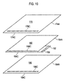
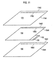
- Figs. 9 to 12 are exploded perspective views for explaining the modified examples 3 to 6 of the first embodiment.
- the resin members 190 can be disposed on the positive-electrode active material layers 165 of the positive electrode 150. In this case, the freedom in disposed positions of the resin members 190 (the bonding positions of the separators 170, 180) is improved.
- the positive electrode and the separators are integrated together, misalignment in the stacking work can be easily suppressed and the laminated cell thus has excellent productivity.
- the positive electrode and the separators are integrated by bonding the portions in both surfaces of the positive electrode and the portions of the separators on the sides facing the both surfaces of the positive electrode. Accordingly, effects on the sizes of the negative electrode, the positive electrode, and the separators are small and the laminated cell can be easily reduced in size. Thus, it is possible to provide a laminated cell which has excellent productivity and which can be easily reduced in size, and a manufacturing method for the same.
- the resin members are electrically insulative, short circuit in the positive-electrode current collecting portion can be suppressed in the case where the resin members are disposed in the electrode collector portion. Furthermore, in the case where the resin members are disposed on the positive-electrode active material layers, the freedom of the disposed positions of the resin members (the bonding positions of the separators) can be improved.
- each of the resin members can be formed of, for example, the double-sided adhesive tape including: an electrically insulative base material; and an adhesive disposed on both surfaces of the base material in the stacking direction.
- the double-sided adhesive tape including: an electrically insulative base material; and an adhesive disposed on both surfaces of the base material in the stacking direction.
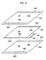
- Fig. 13 is an exploded perspective view for explaining the laminated cell in the second embodiment
- Fig. 14 is an exploded perspective view for explaining a sub-assembly shown in Fig. 13 .
- the members having the same function as those in the first embodiment are denoted by similar reference numerals and description thereof is omitted to avoid overlapping description.
- the second embodiment generally differs from the first embodiment in configurations of a negative electrode, a positive electrode, and current collecting portions.
- a laminated cell 200 in the second embodiment has: an exterior member 210 formed of an upper portion 212 and a lower portion 214; and a laminated body 220 forming a cell main body.
- reference numerals 214A and 214B respectively denote a front edge portion and a rear edge portion of the exterior member 210.
- the laminated body 220 is formed by sequentially stacking negative electrodes 230 and sub-assemblies 222.
- the sub-assemblies 222 each have a positive electrode 250 and separators 270, 280.
- the separators 270, 280 are disposed respectively on both sides of the positive electrode 250 in a stacking direction S.
- a negative-electrode current collecting portion 232 of each negative electrode 230 is disposed substantially at the center of a rear edge portion 234B.
- a positive-electrode current collecting portion 252 of each positive electrode 250 is disposed substantially at the center of a front edge portion 254A. Since the rear edge portion 234B and the front edge portion 254A are opposite and spaced away from each other, the positive-electrode current collecting portion 252 and the negative-electrode current collecting portion 232 do not overlap each other in a stacking direction S.
- reference numeral 234A denotes a front edge portion of each negative electrode 230 while reference numerals 234C, 234D denote side edge portions of each negative electrode 230.
- each sub-assembly 222 film-like resin members (see reference numeral 190 in Fig. 3 ) are bonded to both surfaces of the positive electrode 250 in the stacking direction S. Furthermore, front edge portions 274A, 284A of the separators 270, 280 are bonded to the resin members.
- both surfaces of the positive electrode 250 in the stacking direction S have the front edge portion 254A to which the resin members are bonded, and the separators 270, 280 have the front edge portions 274A, 284A to which the resin members are bonded. Since the positive electrode 250 and the separators 270, 280 are integrated together, misalignment in a stacking work can be easily suppressed and the laminated cell has excellent productivity. Moreover, the positive electrode 250 and the separators 270, 280 are integrated by bonding the outer peripheral portions 254A, 274A, 284A (bonding regions 256, 276, 286) via the resin members.
- reference numeral 259 denotes a bonding region of the positive-electrode current collecting portion 252 to the front edge portion 214A of the exterior member 210.
- Fig. 15 is an exploded perspective view for explaining the modified example 1 of the second embodiment.
- the resin members on both of the positive-electrode current collecting portion 252 and the positive-electrode active material layers, and bond the positive electrode 250 and each of the separators 270, 280 to each other at two positions.
- bonding regions 256 located in the positive-electrode current collecting portion 252 and bonding regions 256A extending along the front edge portion 254A are disposed in the positive electrode 250.
- bonding regions 276, 276A, 286, 286B positioned to face the bonding regions 256, 256A of the positive electrode 250 are disposed in the separators 270, 280. Then, the bonding regions 256, 256A of the positive electrode 250 and the bonding regions 276, 276A of the separator 270 are bonded to one another via a corresponding one of the resin members. Furthermore, the bonding regions 256, 256A of the positive electrode 250 and the bonding regions 286, 286A of the separator 280 are bonded to one another via a corresponding one of the resin members. Accordingly, bonding strength between the positive electrode 250 and each of the separators 270, 280 can be improved.
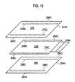
- Figs. 16 to 18 are exploded perspective views for explaining the modified examples 2 to 4 of the second embodiment.
- the resin members can be disposed on the positive-electrode active material layers of the positive electrode 250.
- the arrangement can be similar to that in the modified example 3 (see Fig. 9 ) of the first embodiment.
- Fig. 16 it is possible to dispose the resin members on the positive-electrode active material layers in a rear edge portion 254B of the positive electrode 250, and form bonding regions 256B, 276B, 286B which extend respectively along the rear edge portion 254B and rear edge portions 274B, 284B of the separators 270, 280.
- the arrangement can be similar to that in the modified example 4 (see Fig. 10 ) of the first embodiment.
- Fig. 17 it is possible to dispose the resin members on the positive-electrode active material layers in a side edge portion 254C of the positive electrode 250, and form bonding regions 256C, 276C, 286C which extend respectively along the side edge portion 254C and side edge portions 274C, 284C of the separators 270, 280.
- the resin members can be disposed in a side edge portion 254D as in the modified example 5 (see Fig. 11 ) of the first embodiment.
- the arrangement can be similar to that in the modified example 6 (see Fig. 12 ) of the first embodiment.
- Fig. 18 it is possible to dispose the resin members on the positive-electrode active material layers in both of the side edge portions 254C, 254D of the positive electrode 250, and form the bonding regions 256C, 256D, 276C, 276D, 286C, 286D.
- the second embodiment can provide a laminated cell which has excellent productivity and which can be easily reduced in size, and a manufacturing method for the same.
- Fig. 19 is an exploded perspective view for explaining the laminated cell in the third embodiment.
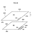
- Fig. 20 is an exploded perspective view for explaining a first sub-assembly shown in Fig. 19 .
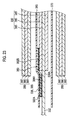
- Fig. 21 is a cross-sectional view for explaining a front portion of the first sub-assembly shown in Fig. 20 .
- Fig. 22 is an exploded perspective view for explaining a second sub-assembly shown in Fig. 19 .
- Fig. 23 is a cross-sectional view for explaining a front portion of the second sub-assembly shown in Fig. 22 .
- the third embodiment generally differs from the first embodiment in the configuration of the sub-assemblies.
- a laminated cell 300 in the third embodiment has: an exterior member 310 formed of an upper portion 312 and a lower portion 314; and a laminated body 320 forming a cell main body.
- reference numerals 314A and 314B respectively denote a front edge portion and a rear edge portion of the exterior member 110.
- the laminated body 320 is formed by sequentially stacking first sub-assemblies 322A and sub-second assemblies 322B below a negative electrode 330.
- each first sub-assembly 322A has a positive electrode 350 and a separator 370.
- each second sub-assembly 322B has the negative electrode 330 and a separator 380.
- the separator 370 and the separator 380 are disposed respectively on one surface of the positive electrode 350 and one surface of the negative electrode 330 in a stacking direction S.
- each negative electrode 330 has a negative-electrode current collector 340, negative-electrode active material layers 345, and a negative-electrode current collecting portion 332.
- an outer peripheral portion of the negative electrode 330 is formed of: a front edge portion 334A in which the negative-electrode current collecting portion 332 is disposed; a rear edge portion 334B which is opposite to the front edge portion 334A; side edge portions 334C, 334D which are opposite to each other and which connect the front edge portion 334A and the rear edge portion 334B to each other.
- a front edge portion 334A in which the negative-electrode current collecting portion 332 is disposed
- a rear edge portion 334B which is opposite to the front edge portion 334A
- side edge portions 334C, 334D which are opposite to each other and which connect the front edge portion 334A and the rear edge portion 334B to each other.
- each positive electrode 350 has a positive-electrode current collector 360, positive-electrode active material layers 365, and a positive-electrode current collecting portion 352. Moreover, an outer peripheral portion of the positive electrode 350 is formed of: a front edge portion 354A in which the positive-electrode current collecting portion 352 is disposed; a rear edge portion 354B which is opposite to the front edge portion; side edge portions 354C, 354D which are opposite to each other and which connect the front edge portion 354A and the rear edge portion 354B to each other.
- outer peripheral portions of the separators 370, 380 include: front edge portions 374A, 384A facing the positive-electrode current collecting portion 352 and the negative-electrode current collecting portion 332; and rear edge portions 374B, 384B opposite to the front edge portions 374A, 384A.
- the outer peripheral portions of the separators 370, 380 also include side edge portions 374C, 384D which are opposite to one another and which connect the front edge portions 374A, 384A and the rear edge portions 374B, 384B to one another.
- each first sub-assembly 322A is formed by bonding the front edge portion 374A of the separator 370 to a resin member 390 bonded to one surface of the positive electrode 350 in the stacking direction S.
- the positive electrode 350 has the front edge portion 354A whose one surface in the stacking direction S is bonded with the resin member 390.
- the positive-electrode current collector 360 and one surface of the resin member 390 are bonded to each other in a bonding region 392A.
- the one surface of the resin member 390 and a corresponding one of the positive-electrode active material layers 365 are bonded to each other in a bonding region 392B.
- the separator 370 has the front edge portion 374A bonded to the resin member 390. In the front edge portion 374A of the separator 370, the separator 370 and the other surface of the resin member 390 are bonded to each other in bonding regions 356, 376.
- the positive electrode 350 and the separator 370 are integrated together via the resin member 390, misalignment in the stacking work can be easily suppressed.
- the integration is performed by bonding the front edge portion 354A (the bonding region 356) which is located on the one surface of the positive electrode 350 and the front edge portion 374A (the bonding region 376) in the separator 370 which is on the side facing the one surface of the positive electrode 350. Accordingly, effects on the sizes of the positive electrode 350 and the separator 370 are small.
- each second sub-assembly 322B is formed by bonding the front edge portion 384A of the separator 380 to the resin member 390 bonded to one surface of the negative electrode 330 in the stacking direction S.
- the negative electrode 330 has the front edge portion 334A whose one surface in the stacking direction S is bonded with the resin member 390.
- the negative-electrode current collector 340 and one surface of the resin member 390 are bonded to each other in the bonding region 392A.
- the one surface of the resin member 390 and a corresponding one of the negative-electrode active material layers 345 are bonded to each other in the bonding region 392B.
- the separator 380 has the front edge portion 384A bonded to the resin member 390. In the front edge portion 384A of the separator 380, the separator 380 and the other surface of the resin member 390 are bonded to each other in bonding regions 336, 386.
- the negative electrode 330 and the separator 380 are integrated together via the resin member 390, misalignment in the stacking work can be easily suppressed.
- the integration is performed by bonding the front edge portion 334A (the bonding region 336) which is located on the one surface of the negative electrode 330 and the front edge portion 384A (the bonding region 386) in the separator 380 which is on the side facing the one surface of the negative electrode 330. Accordingly, effects on the sizes of the negative electrode 330 and the separator 380 are small.
- reference numeral 339 denotes a bonding region of the negative-electrode current collecting portion 332 to the front edge portion 314A of the exterior member 310.
- reference numeral 359 denotes a bonding region of the positive-electrode current collecting portion 352 to the front edge portion 314A of the exterior member 310.
- the positive electrode and the separator as well as the negative electrode and the separator are integrated, misalignment in the stacking work can be easily suppressed and the laminated cell thus has excellent productivity.
- the integration is performed by bonding, via the resin member, the portion which is located on one surface of the positive electrode or the negative electrode and the portion in the separator which is located on the side facing the one surface. Accordingly, effects on the sizes of the negative electrode, the positive electrode, and the separators are small and the laminated cell can be easily reduced in size.
- Fig. 24 is an exploded perspective view for explaining the laminated cell in the fourth embodiment.
- Fig. 25 is an exploded perspective view for explaining a first sub-assembly shown in Fig. 24 .
- Fig. 26 is an exploded perspective view for explaining a second sub-assembly shown in Fig. 24 .
- the fourth embodiment generally differs from the third embodiment in the configurations of current collecting portions of negative electrodes and positive electrodes.
- a laminated cell 400 in the fourth embodiment has: an exterior member 410 formed of an upper portion 412 and a lower portion 414; and a laminated body 420 forming a cell main body.
- reference numerals 414A and 414B respectively denote a front edge portion and a rear edge portion of the exterior member 410.
- the laminated body 420 is formed by sequentially stacking first sub-assemblies 422A and second sub-assemblies 422B below a negative electrode 430.
- each first sub-assembly 422A has a positive electrode 450 and a separator 470.
- each second sub-assembly 422B has the negative electrode 430 and a separator 480.
- the separator 470 and the separator 480 are disposed respectively on one side of the positive electrode 450 and one side of the negative electrode 430 in a stacking direction S.
- a negative-electrode current collecting portion 432 of the negative electrode 430 is disposed substantially at the center of a rear edge portion 434B.
- a positive-electrode current collecting portion 452 of the positive electrode 450 is disposed substantially at the center of a front edge portion 454A. Since the rear edge portion 434B of the negative electrode 430 and the front edge portion 454A of the positive electrode 450 are opposite and spaced away from each other, the positive-electrode current collecting portion 452 and the negative-electrode current collecting portion 432 do not overlap each other in the stacking direction S.
- reference numerals 434A and 434C, 434D denote a front edge portion and side edge portions of the negative electrode 430.
- reference numerals 454B and 454C, 454D denote a rear edge portion and side edge portions of the positive electrode 450.
- each first sub-assembly 422A is formed by bonding a front edge portion 474A of the separator 470 to a resin member (see reference numeral 390 in Fig. 21 ) bonded to one surface of the positive electrode 450 in the stacking direction S.
- the positive electrode 450 has the front edge portion 454A whose one surface in the stacking direction S is bonded with the resin member, and the separator 470 has the front edge portion 474A bonded to the resin member. Since the positive electrode 450 and the separator 470 are integrated, misalignment in the stacking work can be easily suppressed. Moreover, the integration is performed by bonding, via the resin member, the front edge portion 454A (a bonding region 456) which is located on the one surface of the positive electrode 450 and the front edge portion 474A (a bonding region 476) in the separator 470 which is on the side facing the one surface of the positive electrode 450. Accordingly, effects on the sizes of the positive electrode 450 and the separator 470 are small.
- each second sub-assembly 422B is formed by bonding a front edge portion 484A of the separator 480 to the resin member (see reference numeral 390 of Fig. 23 ) bonded to one surface of the negative electrode 430 in the stacking direction S.
- the negative electrode 430 has the rear edge portion 434B whose one surface in the stacking direction S is bonded with the resin member, and the separator 480 has the rear edge portion 484B bonded to the resin member. Since the negative electrode 430 and the separator 480 are integrated, misalignment in the stacking work can be easily suppressed. Moreover, the integration is performed by bonding, via the resin member, the rear edge portion 434B (a bonding region 436) which is located on the one surfaces of the negative electrode 430 and the rear edge portion 484B (a bonding region 486) in the separator 480 which is on the side facing the one surface of the negative electrode 430. Accordingly, effects on the sizes of the negative electrode 430 and the separator 480 are small.
- reference numeral 439 denotes a bonding region of the negative-electrode current collecting portion 432 to the rear edge portion 414B of the exterior member 410.
- reference numeral 459 denotes a bonding region of the positive-electrode current collecting portion 452 to the front edge portion 414A of the exterior member 410.
- the configuration is such that the resin member (separator) is bonded only to one surface of each of the positive electrode and the negative electrode in the stacking direction, and the negative-electrode current collecting portion and the positive-electrode current collecting portion are disposed to be opposite and spaced away from each other. Accordingly, it is possible to provide a laminated cell which has excellent productivity and which can be easily reduced in size, and a manufacturing method for the same.
- the laminated body can be formed in such a way that each sub-assembly is formed of the negative electrode and the separator, and the sub-assemblies and the positive electrodes are sequentially stacked.
- the present invention can be applied to a bipolar secondary cell.
- the modified examples 1 to 6 of the first embodiment and the modified examples 1 to 4 of the second embodiment can be appropriately applied to the third embodiment and the fourth embodiment.
- the separators and at least one of the positive electrode and the negative electrode are integrated together, misalignment in the stacking work can be easily suppressed and the laminated cell has excellent productivity.
- the integration is performed by bonding, via the resin member, the portion which is located on at least one of surfaces of the positive electrode or the negative electrode and the portion in each separator which is located on the side facing the at least one of surfaces. Accordingly, effects on the sizes of the positive electrode, the negative electrode, and the separators are small and the laminated cell can be easily reduced in size. In other words, it is possible to provide a laminated cell which has excellent productivity and which can be easily reduced in size, and a manufacturing method for the same.
Landscapes
- Chemical & Material Sciences (AREA)
- Chemical Kinetics & Catalysis (AREA)
- Electrochemistry (AREA)
- General Chemical & Material Sciences (AREA)
- Engineering & Computer Science (AREA)
- Manufacturing & Machinery (AREA)
- Secondary Cells (AREA)
- Connection Of Batteries Or Terminals (AREA)
- Cell Separators (AREA)
Abstract
Description
- The present invention relates to a laminated cell and a method for manufacturing the same.
- A laminated cell has a laminated body formed by sequentially stacking a positive electrode, a separator, a negative electrode, and a separator. Misalignment in stacking may cause short circuit, reduction of the cell capacity due to reduction in the effective power generation area, and other defects. Thus, the misalignment in stacking is conventionally suppressed by disposing the positive electrode in a bag-shaped separator (see Patent Literature 1, for example).
- Patent Literature 1: Japanese Patent Application Publication No.
Hei 7-302616 - However, in order to position the positive electrode inside the bag-shaped separator, four portions of the bag-shaped separator which correspond to four end surfaces of the positive electrode are thermally fused and bonded. Accordingly, the conventional technique has a problem that the number of work steps is large and improvement in productivity is difficult. Moreover, since the thermal fusion bonding may cause the thickness of the bag-shaped separator to decrease and thereby cause defects such as holes, a certain interval needs to be secured between an outer peripheral portion of the positive electrode and the thermal fusion bonding portion. Accordingly, the conventional technique has a problem that size reduction of the cell through size reduction of the bag-shaped separator is difficult to achieve.
- The present invention has been made in view of such problems of the conventional technique. An object of the present invention is to provide a laminated cell which has excellent productivity and which can be easily reduced in size, and a manufacturing method for the same.
- A laminated cell in a first aspect of the present invention includes a laminated body formed by sequentially stacking a negative electrode, a separator, a positive electrode, and a separator. At least one of surfaces of the positive electrode or the negative electrode in a stacking direction has a portion to which a resin member is bonded, and the separators each has a portion bonded to the resin member on a side facing the at least one of surfaces.
- A method for manufacturing a laminated cell having a laminated body formed by sequentially stacking a negative electrode, a separator, a positive electrode, and a separator in a second aspect of the present invention includes the step of bonding a portion of each of the separators on a side facing at least one of surfaces of the positive electrode or the negative electrode in a stacking direction to a resin member bonded to a portion in the at least one of surfaces.
-
- [
Fig. 1] Fig. 1 is an exploded perspective view for explaining a laminated cell in a first embodiment. - [
Fig. 2] Fig. 2 is an exploded perspective view for explaining a sub-assembly shown inFig. 1 . - [
Fig. 3] Fig. 3 is a cross-sectional view for explaining a front portion of the sub-assembly shown inFig. 1 . - [
Fig. 4] Fig. 4 is a cross-sectional view for explaining a rear portion of the sub-assembly shown inFig. 1 . - [
Fig. 5] Fig. 5 is an exploded perspective view for explaining a modified example 1 of the first embodiment. - [
Fig. 6] Fig. 6 is a cross-sectional view for explaining a current collecting portion in the modified example 1 of the first embodiment. - [
Fig. 7] Fig. 7 is a cross-sectional view for explaining a front edge portion at a position away from the current collecting portion in the modified example 1 of the first embodiment. - [
Fig. 8] Fig. 8 is a cross-sectional view for explaining a modified example 2 of the first embodiment. - [
Fig. 9] Fig. 9 is an exploded perspective view for explaining a modified example 3 of the first embodiment. - [
Fig. 10] Fig. 10 is an exploded perspective view for explaining a modified example 4 of the first embodiment. - [
Fig. 11] Fig. 11 is an exploded perspective view for explaining a modified example 5 of the first embodiment. - [
Fig. 12] Fig. 12 is an exploded perspective view for explaining a modified example 6 of the first embodiment. - [
Fig. 13] Fig. 13 is an exploded perspective view for explaining the laminated cell in a second embodiment. - [
Fig. 14] Fig. 14 is an exploded perspective view for explaining a sub-assembly shown inFig. 13 . - [
Fig. 15] Fig. 15 is an exploded perspective view for explaining a modified example 1 of the second embodiment. - [
Fig. 16] Fig. 16 is an exploded perspective view for explaining a modified example 2 of the second embodiment. - [
Fig. 17] Fig. 17 is an exploded perspective view for explaining a modified example 3 of the second embodiment. - [
Fig. 18] Fig. 18 is an exploded perspective view for explaining a modified example 4 of the second embodiment. - [
Fig. 19] Fig. 19 is an exploded perspective view for explaining the laminated cell in a third embodiment. - [
Fig. 20] Fig. 20 is an exploded perspective view for explaining a first sub-assembly shown inFig. 19 . - [
Fig. 21] Fig. 21 is a cross-sectional view for explaining a front portion of the first sub-assembly shown inFig. 20 . - [
Fig. 22] Fig. 22 is an exploded perspective view for explaining a second sub-assembly shown inFig. 19 . - [
Fig. 23] Fig. 23 is a cross-sectional view for explaining a front portion of the second sub-assembly shown inFig. 22 . - [
Fig. 24] Fig. 24 is an exploded perspective view for explaining the laminated cell in a fourth embodiment. - [
Fig. 25] Fig. 25 is an exploded perspective view for explaining a first sub-assembly shown inFig. 24 . - [
Fig. 26] Fig. 26 is an exploded perspective view for explaining a second sub-assembly shown inFig. 24 . - Embodiments of the present invention are described below based on the drawings. Note that proportions of dimensions in the drawings may be exaggerated for the sake of description and be different from the actual proportions.
-
Fig. 1 is an exploded perspective view for explaining a laminated cell in a first embodiment andFig. 2 is an exploded perspective view for explaining a sub-assembly shown inFig. 1 . Moreover,Figs. 3 and4 are cross-sectional views respectively for explaining a front portion and a rear portion of the sub-assembly shown inFig. 1 . - A laminated
cell 100 in the first embodiment is formed of, for example, a substantially-rectangular lithium-ion secondary cell and has anexterior member 110 and a laminatedbody 120 forming a cell main body. - The
exterior member 110 is formed of anupper portion 112 and alower portion 114 and is used to prevent shock from the outside and deterioration due to an environment. Outer peripheral portions of sheet members forming theupper portion 112 and thelower portion 114 are partially or entirely bonded to each other by thermal fusion bonding. From the view point of weight reduction and thermal conductivity, the sheet members in theexterior member 110 are preferably made of polymer-metal composite laminated film in which a metal is covered with an insulator such as a polypropylene film. A metal such as aluminum, stainless steel, nickel, or copper or an alloy of these metals can be used as the metal in the sheet members. Note thatreference numerals exterior member 110. - The laminated
body 120 is formed by sequentially stackingnegative electrodes 130 andsub-assemblies 122. Thesub-assemblies 122 each have apositive electrode 150 andseparators separators positive electrode 150 in a stacking direction S. The number of the stackednegative electrodes 130 and thestacked sub-assemblies 122 is determined as appropriate in consideration of the required capacity and the like. - As shown in
Figs. 1 and3 , eachnegative electrode 130 has a substantially-rectangular shape and has a negative-electrodecurrent collector 140 and negative-electrodeactive material layers 145. The negative-electrodecurrent collector 140 is formed of a high-conductivity member and has a negative-electrodecurrent collecting portion 132 for taking out generated electric power to the outside. The negative-electrodeactive material layers 145 are regions in which a negative-electrode active material is disposed, the negative-electrode active material being a material to which lithium is inserted and from which lithium is extracted. The negative-electrode active material layers 145 are disposed on both surfaces of the negative-electrodecurrent collector 140 except for the negative-electrodecurrent collecting portion 132 and are in contact with the negative-electrodecurrent collector 140. An outer peripheral portion of thenegative electrode 130 is formed of: afront edge portion 134A in which the negative-electrodecurrent collecting portion 132 is disposed; arear edge portion 134B which is opposite to the front edge portion; andside edge portions front edge portion 134A and therear edge portion 134B to each other. - Moreover, as shown in
Figs. 2 and3 , eachpositive electrode 150 has a substantially-rectangular shape and has a positive-electrodecurrent collector 160 and positive-electrode active material layers 165. The positive-electrodecurrent collector 160 is formed of a high-conductivity member and has a positive-electrodecurrent collecting portion 152 for taking out the generated electric power to the outside. The positive-electrode active material layers 165 are regions in which a positive-electrode active material is disposed, the positive-electrode active material being a material to which lithium is inserted and from which lithium is extracted. The positive-electrode active material layers 165 are disposed on both surfaces of the positive-electrodecurrent collector 160 except for the positive-electrodecurrent collecting portion 152 and are in contact with the positive-electrodecurrent collector 160. An outer peripheral portion of thepositive electrode 150 is formed of: afront edge portion 154A in which the positive-electrodecurrent collecting portion 152 is disposed; arear edge portion 154B which is opposite to the front edge portion; andside edge portions front edge portion 154A and therear edge portion 154B to each other. Note thatreference numeral 159 denotes a bonding region of the positive-electrodecurrent collecting portion 152 to thefront edge portion 114A of theexterior member 110. - In the embodiment, as shown in
Figs. 3 and4 , thenegative electrodes 130 are formed to be larger than thepositive electrodes 150 in size. The negative-electrodecurrent collecting portions 132 and the positive-electrodecurrent collecting portions 152 extend to the outside of the cell from a space between theupper portion 112 and thelower portion 114 of theexterior member 110. Moreover, in order to secure the tightness of theexterior member 110, contact portions of the negative-electrodecurrent collecting portions 132 and the positive-electrodecurrent collecting portions 152 with theexterior member 110 are bonded. Moreover, as shown inFig. 1 , the positions and shapes of the negative-electrodecurrent collecting portions 132 and the positive-electrodecurrent collecting portions 152 are set such that the negative-electrodecurrent collecting portions 132 and the positive-electrodecurrent collecting portions 152 do not overlap one another in the stacking direction S. - The
separators separators negative electrode 130 and thepositive electrode 150. Moreover, as shown inFigs. 3 and4 , theseparators Fig. 2 , outer peripheral portions of theseparators front edge portions current collecting portion 152 and the negative-electrodecurrent collecting portion 132; andrear edge portions front edge portions separators side edge portions front edge portions rear edge portions - Moreover, as shown in
Fig. 3 , in each sub-assembly 122, film-like resin members 190 are bonded to both surfaces of thepositive electrode 150 in the stacking direction S. Furthermore, thefront edge portions separators resin members 190, respectively. - In other words, the
electrode 150 has thefront edge portion 154A whose both surfaces in the stacking direction S are bonded with theresin members 190. In thefront edge portion 154A, the positive-electrodecurrent collector 160 and one surfaces of theresin members 190 are bonded to one another inbonding regions 192A. Moreover, the positive-electrodeactive material layer 165 and the one surfaces of theresin members 190 are bonded to one another inbonding regions 192B. Furthermore, theseparators front edge portions resin members 190 are bonded. In thefront edge portion 174A of theseparator 170, theseparator 170 and the other surface of a corresponding one of theresin members 190 are bonded to each other inbonding regions front edge portion 184A of theseparator 180, theseparator 180 and the other surface of a corresponding one of theresin members 190 are bonded to each other inbonding regions - Since the
positive electrode 150 and theseparators resin members 190 as described above, misalignment in a stacking work can be easily suppressed and the laminated cell has excellent productivity. In other words, the positioning in the stacking work is facilitated and the workability is improved. Moreover, thefront edge portion 154A (bonding regions 156) is provided on both surfaces of thepositive electrode 150 while thefront edge portions bonding regions 176, 186) facing thefront edge portion 154A on both surfaces of thepositive electrode 150 are provided in theseparators positive electrode 150 and theseparators front edge portion 154A (bonding regions 156) of thepositive electrode 150 to thefront edge portions bonding regions 176, 186) of theseparators negative electrode 130, thepositive electrode 150, and theseparators laminated cell 100 can be thereby easily reduced in size. Thus, it is possible to provide a laminated cell which has excellent productivity and which can be easily reduced in size, and a manufacturing method for the same. - Note that the
resin members 190 have an electrically insulating characteristic and are arranged in the positive-electrodecurrent collecting portion 152 in the embodiment. Accordingly, short circuit in the positive-electrodecurrent collecting portion 152 can be also prevented. - The bonding method of the
resin members 190 to thepositive electrode 150 and the bonding method of theseparators resin members 190 are not limited and methods such as thermal welding, ultrasonic welding, laser welding, induction heating welding, and an adhesive can be used as appropriate. Moreover, the mode of each of the bonding regions is not limited to a mode including a single dot-shaped region and can be a mode including multiple dot-shaped regions which are, for example, a group of dot-shaped regions spaced away from each other. - Each of the
resin members 190 may be formed of, for example, a double-sided adhesive tape including: an electrically insulative base material; and an adhesive disposed on both surfaces of the base material in the stacking direction S. In this case, there is no need to, for example, dispose an adhesive or use a thermal fusion bonding device for the bonding of thepositive electrode 150 and theresin members 190 and the bonding of theseparators resin members 190. Accordingly, it is possible to reduce the number of work steps and improve productivity. - Examples of the base material which can be used in the
resin members 190 include a resin selected from a group including polypropylene, polyethylene, and polyamide-based synthetic fiber. The base material can be made of a single layer or a laminated body in which multiple layers are stacked. Moreover, examples of the adhesive include a material which has resistance to solvent and which is selected from a group including synthetic rubbers, butyl rubber, synthetic resins, and acryl. - A carbon material and an alloy-based negative-electrode material are preferably used as the negative-electrode active material in the negative-electrode active material layers 145 of the
negative electrodes 130, from the view point of capacity and output characteristics. For example, graphite, carbon black, activated carbon, carbon fiber, coke, soft carbon, and hard carbon are preferably used as the carbon material. A lithium-transition metal complex oxide is preferably used as the positive-electrode active material in the positive-electrode active material layers 165 of thepositive electrodes 150, from the view point of capacity and output characteristics. For example, a Li-Co-based complex oxide such as LiCoO2, a Li-Ni-based complex oxide such as LiNiO2, a Li-Mn-based complex oxide such as a spinel LiMn2O4, and LiFeO2 are preferably used as the lithium-transition metal complex oxide. The alloy-based negative-electrode material preferably contains an element which can form an alloy with lithium, such as silicon, silicon oxide, tin dioxide, silicon carbide, and tin. - The negative-electrode active material layers 145 and the positive-electrode active material layers 165 may further contain additives such as a binder and a conductive additive. For example, polyamic acid, polyethylene (PE), polypropylene (PP), polyethylene terephthalate (PET), polyether nitrile (PEN), polyimide (PI), polyamide (PA), polytetrafluoroethylene (PTFE), styrene-butadiene rubber (SBR), polyacrylonitrile (PAN), poly(methyl acrylate) (PMA), poly(methyl methacrylate) (PMMA), polyvinyl chloride (PVC), polyvinylidene difluoride (PVdF), or a mixture of these materials are preferably used as the binder. Moreover, the conductive additive is an additive blended to improve the conductivity of the negative-electrode active material layers 145 and the positive-electrode active material layers 165. For example, carbon materials such as graphite, vapor-grown carbon fiber, and carbon black which is, for examples, acetylene black or the like are preferably used as the conductive additive.
- For example, iron, stainless-steel, chrome, nickel, manganese, titanium, molybdenum, vanadium, niobium, aluminum, copper, silver, gold, platinum, and carbon can be used as the material of the negative-electrode
current collectors 140 and the positive-electrodecurrent collectors 160. Aluminum and copper are preferable as the material of the negative-electrodecurrent collectors 140 and the positive-electrodecurrent collectors 160, from the view point of electron conductivity and cell operating potential. - The
separators separators - An electrolyte permeates the
separators separators separators - The liquid electrolyte which can be contained in the
separators - Polymer electrolytes which can be contained in the
separators - Next, modified examples 1 to 6 of the first embodiment are described one by one.
Fig. 5 is an exploded perspective view for explaining the modified example 1 of the first embodiment.Fig. 6 is a cross-sectional view for explaining a current collecting portion in the modified example 1 of the first embodiment.Fig. 7 is a cross-sectional view for explaining a front edge portion at a position away from the current collecting portion in the modified example 1 of the first embodiment.Fig. 8 is a cross-sectional view for explaining the modified example 2 of the first embodiment. - In the modified example 1, the
resin members 190 are disposed on both of the positive-electrodecurrent collecting portion 152 and the positive-electrode active material layers 165, and thepositive electrode 150 and each of theseparators front edge portion 154A of thepositive electrode 150, the positive-electrodecurrent collector 160 and the one surfaces of theresin members 190 are bonded to one another in thebonding regions 192A. Moreover, the positive-electrode active material layers 165 and the one surfaces of theresin members 190 are bonded to one another in thebonding regions 192B. Furthermore, in thefront edge portion 174A of theseparator 170, theseparator 170 and the other surface of the correspondingresin member 190 are bonded to each other in thebonding regions front edge portion 184A of theseparator 180, theseparator 180 and the other surface of the correspondingresin member 190 are bonded to each other in thebonding regions - In addition, in the modified example 1, the
positive electrode 150 to which theresin members 190 are bonded hasbonding regions 156A extending along thefront edge portion 154A. Moreover, theseparators bonding regions bonding regions positive electrode 150. In theseparator 170, theseparator 170 and the other surface of the correspondingresin member 190 are bonded to each other in thebonding regions separator 180, theseparator 180 and the other surface of the correspondingresin member 190 are bonded to each other in thebonding regions positive electrode 150 and each of theresin members 190 are bonded to each other at two portions in thebonding regions separator 170 and the correspondingresin member 190 are bonded to each other at two positions in thebonding regions separator 180 and the correspondingresin member 190 are bonded to each other at two positions in thebonding regions positive electrode 150 and each of theseparators - As shown in the modified example 2 of
Fig. 8 , the bonding between theresin members 190 and theseparators current collecting portion 152 can be omitted as necessary. In other words, the laminated cell may be configured such that nobonding regions Fig. 6 are provided and that theseparator 170 and the correspondingresin member 190 are bonded to each other at one position in thebonding regions separator 180 and the correspondingresin member 190 are bonded to each other at one position in thebonding regions -
Figs. 9 to 12 are exploded perspective views for explaining the modified examples 3 to 6 of the first embodiment. Theresin members 190 can be disposed on the positive-electrode active material layers 165 of thepositive electrode 150. In this case, the freedom in disposed positions of the resin members 190 (the bonding positions of theseparators 170, 180) is improved. - For example, as shown in
Fig. 9 , it is possible to dispose theresin members 190 on the positive-electrode active material layers 165 in therear edge portion 154B of thepositive electrode 150, andform bonding regions rear edge portion 154B of thepositive electrode 150 and therear edge portions separators 170, 180 (the modified example 3). - Moreover, as shown in
Fig. 10 , it is possible to dispose theresin members 190 on the positive-electrode active material layers 165 in theside edge portion 154C of thepositive electrode 150, andform bonding regions side edge portion 154C of thepositive electrode 150 and theside edge portions separators 170, 180 (the modified example 4). - Furthermore, as shown in
Fig. 11 , it is possible to dispose theresin members 190 on the positive-electrode active material layers 165 in theside edge portion 154D, andform bonding regions side edge portion 154D of thepositive electrode 150 and theside edge portions separators 170, 180 (the modified example 5). - Moreover, as shown in
Fig. 12 , it is possible to dispose theresin members 190 on the positive-electrode active material layers 165 in both of theside edge portions positive electrode 150, and form thebonding regions - As described above, in the first embodiment, since the positive electrode and the separators are integrated together, misalignment in the stacking work can be easily suppressed and the laminated cell thus has excellent productivity. Moreover, the positive electrode and the separators are integrated by bonding the portions in both surfaces of the positive electrode and the portions of the separators on the sides facing the both surfaces of the positive electrode. Accordingly, effects on the sizes of the negative electrode, the positive electrode, and the separators are small and the laminated cell can be easily reduced in size. Thus, it is possible to provide a laminated cell which has excellent productivity and which can be easily reduced in size, and a manufacturing method for the same.
- Moreover, since the resin members are electrically insulative, short circuit in the positive-electrode current collecting portion can be suppressed in the case where the resin members are disposed in the electrode collector portion. Furthermore, in the case where the resin members are disposed on the positive-electrode active material layers, the freedom of the disposed positions of the resin members (the bonding positions of the separators) can be improved.
- In addition, each of the resin members can be formed of, for example, the double-sided adhesive tape including: an electrically insulative base material; and an adhesive disposed on both surfaces of the base material in the stacking direction. In this case, there is no need to, for example, dispose an adhesive or use a thermal bonding device for the bonding of the separators. Accordingly, it is possible to reduce the number of work steps and improve productivity.
- Next, a laminated cell in a second embodiment is described.
Fig. 13 is an exploded perspective view for explaining the laminated cell in the second embodiment andFig. 14 is an exploded perspective view for explaining a sub-assembly shown inFig. 13 . In the following description, the members having the same function as those in the first embodiment are denoted by similar reference numerals and description thereof is omitted to avoid overlapping description. - The second embodiment generally differs from the first embodiment in configurations of a negative electrode, a positive electrode, and current collecting portions. Specifically, as shown in
Fig. 13 , alaminated cell 200 in the second embodiment has: anexterior member 210 formed of anupper portion 212 and alower portion 214; and alaminated body 220 forming a cell main body. Note thatreference numerals exterior member 210. - The
laminated body 220 is formed by sequentially stackingnegative electrodes 230 andsub-assemblies 222. Thesub-assemblies 222 each have apositive electrode 250 andseparators separators positive electrode 250 in a stacking direction S. - A negative-electrode
current collecting portion 232 of eachnegative electrode 230 is disposed substantially at the center of arear edge portion 234B. A positive-electrodecurrent collecting portion 252 of eachpositive electrode 250 is disposed substantially at the center of afront edge portion 254A. Since therear edge portion 234B and thefront edge portion 254A are opposite and spaced away from each other, the positive-electrodecurrent collecting portion 252 and the negative-electrodecurrent collecting portion 232 do not overlap each other in a stacking direction S. Note that reference numeral 234A denotes a front edge portion of eachnegative electrode 230 whilereference numerals negative electrode 230. - Moreover, as shown in
Fig. 14 , in each sub-assembly 222, film-like resin members (seereference numeral 190 inFig. 3 ) are bonded to both surfaces of thepositive electrode 250 in the stacking direction S. Furthermore,front edge portions separators - In other words, both surfaces of the
positive electrode 250 in the stacking direction S have thefront edge portion 254A to which the resin members are bonded, and theseparators front edge portions positive electrode 250 and theseparators positive electrode 250 and theseparators peripheral portions bonding regions negative electrode 230, thepositive electrode 250, and theseparators laminated cell 200 can be easily reduced in size. Thus, it is possible to provide a laminated cell which has excellent productivity and which can be easily reduced in size, and a manufacturing method for the same. Note thatreference numeral 259 denotes a bonding region of the positive-electrodecurrent collecting portion 252 to thefront edge portion 214A of theexterior member 210. - Next, modified examples 1 to 4 of the second embodiment are sequentially described.
-
Fig. 15 is an exploded perspective view for explaining the modified example 1 of the second embodiment. As in the modified example 1 (seeFig. 5 ) of the first embodiment, it is possible to dispose the resin members on both of the positive-electrodecurrent collecting portion 252 and the positive-electrode active material layers, and bond thepositive electrode 250 and each of theseparators bonding regions 256 located in the positive-electrodecurrent collecting portion 252 andbonding regions 256A extending along thefront edge portion 254A are disposed in thepositive electrode 250. Moreover,bonding regions bonding regions positive electrode 250 are disposed in theseparators bonding regions positive electrode 250 and thebonding regions separator 270 are bonded to one another via a corresponding one of the resin members. Furthermore, thebonding regions positive electrode 250 and thebonding regions separator 280 are bonded to one another via a corresponding one of the resin members. Accordingly, bonding strength between thepositive electrode 250 and each of theseparators -
Figs. 16 to 18 are exploded perspective views for explaining the modified examples 2 to 4 of the second embodiment. In order to improve the freedom in disposed positions of the resin members 290 (the bonding positions of theseparators 270, 280), the resin members can be disposed on the positive-electrode active material layers of thepositive electrode 250. - For example, the arrangement can be similar to that in the modified example 3 (see
Fig. 9 ) of the first embodiment. Specifically, as shown inFig. 16 , it is possible to dispose the resin members on the positive-electrode active material layers in arear edge portion 254B of thepositive electrode 250, andform bonding regions rear edge portion 254B andrear edge portions separators - Moreover, the arrangement can be similar to that in the modified example 4 (see
Fig. 10 ) of the first embodiment. Specifically, as shown inFig. 17 , it is possible to dispose the resin members on the positive-electrode active material layers in aside edge portion 254C of thepositive electrode 250, andform bonding regions side edge portion 254C andside edge portions separators side edge portion 254D as in the modified example 5 (seeFig. 11 ) of the first embodiment. - Moreover, the arrangement can be similar to that in the modified example 6 (see
Fig. 12 ) of the first embodiment. Specifically, as shown inFig. 18 , it is possible to dispose the resin members on the positive-electrode active material layers in both of theside edge portions positive electrode 250, and form thebonding regions - As described above, in a case where a laminated cell has a configuration in which a negative-electrode current collecting portion and a positive-electrode current collecting portion are opposite and spaced away from each other, the second embodiment can provide a laminated cell which has excellent productivity and which can be easily reduced in size, and a manufacturing method for the same.
- Next, a laminated cell in a third embodiment is described.
Fig. 19 is an exploded perspective view for explaining the laminated cell in the third embodiment.Fig. 20 is an exploded perspective view for explaining a first sub-assembly shown inFig. 19 .Fig. 21 is a cross-sectional view for explaining a front portion of the first sub-assembly shown inFig. 20 .Fig. 22 is an exploded perspective view for explaining a second sub-assembly shown inFig. 19 .Fig. 23 is a cross-sectional view for explaining a front portion of the second sub-assembly shown inFig. 22 . - The third embodiment generally differs from the first embodiment in the configuration of the sub-assemblies. Specifically, a
laminated cell 300 in the third embodiment has: anexterior member 310 formed of anupper portion 312 and alower portion 314; and alaminated body 320 forming a cell main body. Note thatreference numerals exterior member 110. - As shown in
Fig. 19 , thelaminated body 320 is formed by sequentially stackingfirst sub-assemblies 322A andsub-second assemblies 322B below anegative electrode 330. As shown inFig. 20 , eachfirst sub-assembly 322A has apositive electrode 350 and aseparator 370. As shown inFig. 22 , eachsecond sub-assembly 322B has thenegative electrode 330 and aseparator 380. Theseparator 370 and theseparator 380 are disposed respectively on one surface of thepositive electrode 350 and one surface of thenegative electrode 330 in a stacking direction S. - As shown in
Figs. 21 and22 , eachnegative electrode 330 has a negative-electrodecurrent collector 340, negative-electrode active material layers 345, and a negative-electrodecurrent collecting portion 332. Moreover, an outer peripheral portion of thenegative electrode 330 is formed of: afront edge portion 334A in which the negative-electrodecurrent collecting portion 332 is disposed; arear edge portion 334B which is opposite to thefront edge portion 334A;side edge portions front edge portion 334A and therear edge portion 334B to each other. As shown inFigs. 20 and21 , eachpositive electrode 350 has a positive-electrodecurrent collector 360, positive-electrode active material layers 365, and a positive-electrodecurrent collecting portion 352. Moreover, an outer peripheral portion of thepositive electrode 350 is formed of: afront edge portion 354A in which the positive-electrodecurrent collecting portion 352 is disposed; arear edge portion 354B which is opposite to the front edge portion;side edge portions front edge portion 354A and therear edge portion 354B to each other. - As shown in
Figs. 20 and22 , outer peripheral portions of theseparators front edge portions current collecting portion 352 and the negative-electrodecurrent collecting portion 332; andrear edge portions front edge portions separators side edge portions front edge portions rear edge portions - As shown in
Fig. 21 , eachfirst sub-assembly 322A is formed by bonding thefront edge portion 374A of theseparator 370 to aresin member 390 bonded to one surface of thepositive electrode 350 in the stacking direction S. - In other words, the
positive electrode 350 has thefront edge portion 354A whose one surface in the stacking direction S is bonded with theresin member 390. In thefront edge portion 354A, the positive-electrodecurrent collector 360 and one surface of theresin member 390 are bonded to each other in abonding region 392A. Furthermore, the one surface of theresin member 390 and a corresponding one of the positive-electrode active material layers 365 are bonded to each other in abonding region 392B. Moreover, theseparator 370 has thefront edge portion 374A bonded to theresin member 390. In thefront edge portion 374A of theseparator 370, theseparator 370 and the other surface of theresin member 390 are bonded to each other inbonding regions - As described above, since the
positive electrode 350 and theseparator 370 are integrated together via theresin member 390, misalignment in the stacking work can be easily suppressed. Moreover, the integration is performed by bonding thefront edge portion 354A (the bonding region 356) which is located on the one surface of thepositive electrode 350 and thefront edge portion 374A (the bonding region 376) in theseparator 370 which is on the side facing the one surface of thepositive electrode 350. Accordingly, effects on the sizes of thepositive electrode 350 and theseparator 370 are small. - Moreover, as shown in
Fig. 23 , eachsecond sub-assembly 322B is formed by bonding thefront edge portion 384A of theseparator 380 to theresin member 390 bonded to one surface of thenegative electrode 330 in the stacking direction S. - In other words, the
negative electrode 330 has thefront edge portion 334A whose one surface in the stacking direction S is bonded with theresin member 390. In thefront edge portion 334A, the negative-electrodecurrent collector 340 and one surface of theresin member 390 are bonded to each other in thebonding region 392A. Furthermore, the one surface of theresin member 390 and a corresponding one of the negative-electrode active material layers 345 are bonded to each other in thebonding region 392B. Moreover, theseparator 380 has thefront edge portion 384A bonded to theresin member 390. In thefront edge portion 384A of theseparator 380, theseparator 380 and the other surface of theresin member 390 are bonded to each other inbonding regions - As described above, since the
negative electrode 330 and theseparator 380 are integrated together via theresin member 390, misalignment in the stacking work can be easily suppressed. Moreover, the integration is performed by bonding thefront edge portion 334A (the bonding region 336) which is located on the one surface of thenegative electrode 330 and thefront edge portion 384A (the bonding region 386) in theseparator 380 which is on the side facing the one surface of thenegative electrode 330. Accordingly, effects on the sizes of thenegative electrode 330 and theseparator 380 are small. - Note that
reference numeral 339 denotes a bonding region of the negative-electrodecurrent collecting portion 332 to thefront edge portion 314A of theexterior member 310. Moreover,reference numeral 359 denotes a bonding region of the positive-electrodecurrent collecting portion 352 to thefront edge portion 314A of theexterior member 310. - As described above, in the third embodiment, since the positive electrode and the separator as well as the negative electrode and the separator are integrated, misalignment in the stacking work can be easily suppressed and the laminated cell thus has excellent productivity. Moreover, the integration is performed by bonding, via the resin member, the portion which is located on one surface of the positive electrode or the negative electrode and the portion in the separator which is located on the side facing the one surface. Accordingly, effects on the sizes of the negative electrode, the positive electrode, and the separators are small and the laminated cell can be easily reduced in size. Thus, in a case where a bonding member (separator) is bonded only to one surface of a positive electrode or a negative electrode in the stacking direction, it is possible to provide a laminated cell which has excellent productivity and which can be easily reduced in size, and a manufacturing method for the same.
- Next, a laminated cell in a fourth embodiment is described.
Fig. 24 is an exploded perspective view for explaining the laminated cell in the fourth embodiment.Fig. 25 is an exploded perspective view for explaining a first sub-assembly shown inFig. 24 .Fig. 26 is an exploded perspective view for explaining a second sub-assembly shown inFig. 24 . - The fourth embodiment generally differs from the third embodiment in the configurations of current collecting portions of negative electrodes and positive electrodes. Specifically, as shown in
Fig. 24 , alaminated cell 400 in the fourth embodiment has: anexterior member 410 formed of anupper portion 412 and alower portion 414; and alaminated body 420 forming a cell main body. Note thatreference numerals exterior member 410. - As shown in
Fig. 24 , thelaminated body 420 is formed by sequentially stackingfirst sub-assemblies 422A andsecond sub-assemblies 422B below anegative electrode 430. As shown inFig. 25 , eachfirst sub-assembly 422A has apositive electrode 450 and aseparator 470. As shown inFig. 26 , eachsecond sub-assembly 422B has thenegative electrode 430 and aseparator 480. Theseparator 470 and theseparator 480 are disposed respectively on one side of thepositive electrode 450 and one side of thenegative electrode 430 in a stacking direction S. - As shown in
Fig. 26 , a negative-electrodecurrent collecting portion 432 of thenegative electrode 430 is disposed substantially at the center of arear edge portion 434B. As shown inFig. 25 , a positive-electrodecurrent collecting portion 452 of thepositive electrode 450 is disposed substantially at the center of afront edge portion 454A. Since therear edge portion 434B of thenegative electrode 430 and thefront edge portion 454A of thepositive electrode 450 are opposite and spaced away from each other, the positive-electrodecurrent collecting portion 452 and the negative-electrodecurrent collecting portion 432 do not overlap each other in the stacking direction S. Note thatreference numerals negative electrode 430. Moreover,reference numerals positive electrode 450. - As shown in
Fig. 25 , eachfirst sub-assembly 422A is formed by bonding afront edge portion 474A of theseparator 470 to a resin member (seereference numeral 390 inFig. 21 ) bonded to one surface of thepositive electrode 450 in the stacking direction S. - In other words, the
positive electrode 450 has thefront edge portion 454A whose one surface in the stacking direction S is bonded with the resin member, and theseparator 470 has thefront edge portion 474A bonded to the resin member. Since thepositive electrode 450 and theseparator 470 are integrated, misalignment in the stacking work can be easily suppressed. Moreover, the integration is performed by bonding, via the resin member, thefront edge portion 454A (a bonding region 456) which is located on the one surface of thepositive electrode 450 and thefront edge portion 474A (a bonding region 476) in theseparator 470 which is on the side facing the one surface of thepositive electrode 450. Accordingly, effects on the sizes of thepositive electrode 450 and theseparator 470 are small. - Moreover, as shown in
Fig. 26 , eachsecond sub-assembly 422B is formed by bonding afront edge portion 484A of theseparator 480 to the resin member (seereference numeral 390 ofFig. 23 ) bonded to one surface of thenegative electrode 430 in the stacking direction S. - In other words, the
negative electrode 430 has therear edge portion 434B whose one surface in the stacking direction S is bonded with the resin member, and theseparator 480 has therear edge portion 484B bonded to the resin member. Since thenegative electrode 430 and theseparator 480 are integrated, misalignment in the stacking work can be easily suppressed. Moreover, the integration is performed by bonding, via the resin member, therear edge portion 434B (a bonding region 436) which is located on the one surfaces of thenegative electrode 430 and therear edge portion 484B (a bonding region 486) in theseparator 480 which is on the side facing the one surface of thenegative electrode 430. Accordingly, effects on the sizes of thenegative electrode 430 and theseparator 480 are small. - Note that
reference numeral 439 denotes a bonding region of the negative-electrodecurrent collecting portion 432 to therear edge portion 414B of theexterior member 410. Moreover,reference numeral 459 denotes a bonding region of the positive-electrodecurrent collecting portion 452 to thefront edge portion 414A of theexterior member 410. - As described above, in the fourth embodiment, the configuration is such that the resin member (separator) is bonded only to one surface of each of the positive electrode and the negative electrode in the stacking direction, and the negative-electrode current collecting portion and the positive-electrode current collecting portion are disposed to be opposite and spaced away from each other. Accordingly, it is possible to provide a laminated cell which has excellent productivity and which can be easily reduced in size, and a manufacturing method for the same.
- The present invention is not limited to the embodiments described above and various modifications can be made. For example, the laminated body can be formed in such a way that each sub-assembly is formed of the negative electrode and the separator, and the sub-assemblies and the positive electrodes are sequentially stacked.
- Moreover, the present invention can be applied to a bipolar secondary cell. Furthermore, the modified examples 1 to 6 of the first embodiment and the modified examples 1 to 4 of the second embodiment can be appropriately applied to the third embodiment and the fourth embodiment.
- The entire contents of Japanese Patent Application No.
2011-137704 (filed June 21, 2011 2012-036530 (filed February 22, 2012 - The contents of the present invention have been described above according to the embodiments. However, the present invention is not limited to these descriptions and it is apparent to those skilled in the art that various modifications and improvements can be made.
- In the present invention, since the separators and at least one of the positive electrode and the negative electrode are integrated together, misalignment in the stacking work can be easily suppressed and the laminated cell has excellent productivity. Moreover, the integration is performed by bonding, via the resin member, the portion which is located on at least one of surfaces of the positive electrode or the negative electrode and the portion in each separator which is located on the side facing the at least one of surfaces. Accordingly, effects on the sizes of the positive electrode, the negative electrode, and the separators are small and the laminated cell can be easily reduced in size. In other words, it is possible to provide a laminated cell which has excellent productivity and which can be easily reduced in size, and a manufacturing method for the same.
-
- 100, 200, 300, 400
- laminated cell
- 110, 210, 310, 410
- exterior member
- 120, 220, 320, 420
- laminated body
- 130, 230, 330, 430
- negative electrode
- 132, 232, 332, 432
- negative-electrode current collecting portion
- 140, 340
- negative-electrode current collector
- 145, 345
- negative-electrode active material layer
- 150, 250, 350, 450
- positive electrode
- 152, 252, 352,452
- positive-electrode current collecting portion
- 160, 360
- positive-electrode current collector
- 165, 365
- positive-electrode active material layer
- 170, 180, 270, 280, 370, 380, 470, 480
- separator
- 190, 390
- resin member
- S
- stacking direction
Claims (10)
- A laminated cell comprising a laminated body formed by sequentially stacking a negative electrode, a separator, a positive electrode, and a separator, wherein
at least one of surfaces of the positive electrode or the negative electrode in a stacking direction has a portion to which a resin member is bonded, and
the separators each have a portion bonded to the resin member on a side facing at least one of the surfaces. - The laminated cell according to claim 1, wherein
both of the surfaces of the positive electrode or the negative electrode in the stacking direction have portions to which the resin members are bonded, and
the separators have portions bonded to the resin members on sides facing both of the surfaces. - The laminated cell according to claim 1 or 2, wherein
the positive electrode and the negative electrode have current collecting portions for taking out generated electricity to the outside, and
the resin member is electrically insulative and is disposed in at least each of the current collecting portions. - The laminated cell according to any one of claims 1 to 3, wherein the resin member is disposed in at least a region in which an active material is disposed.
- The laminated cell according to any one of claims 1 to 4, wherein the resin member has: an electrically insulative base member; and an adhesive disposed on both surfaces of the base member in the stacking direction.
- A method for manufacturing a laminated cell having a laminated body formed by sequentially stacking a negative electrode, a separator, a positive electrode, and a separator, the method comprising the step of bonding a portion of each of the separators on a side facing at least one of surfaces of the positive electrode or the negative electrode in a stacking direction to a resin member bonded to a portion located on at least one of the surfaces.
- The method for manufacturing the laminated cell according to claim 6, wherein portions of the separators are bonded to the resin members bonded to portions located on both of the surfaces of the positive electrode or the negative electrode in the stacking direction, the portions of the separators being on sides facing both of the surfaces.
- The method for manufacturing the laminated cell according to claim 6 or 7, wherein
the positive electrode and the negative electrode have current collecting portions for taking out generated electricity to the outside, and the resin members are electrically insulative, and
the resin member is disposed in at least each of the current collecting portions. - The method for manufacturing the laminated cell according to any one of claims 6 to 8, wherein the resin member is disposed in at least a region in which an active material is disposed.
- The method for manufacturing the laminated cell according to any one of claims 6 to 9, wherein the resin member has: an electrically insulative base member; and an adhesive disposed on both surfaces of the base member in the stacking direction.
Applications Claiming Priority (3)
| Application Number | Priority Date | Filing Date | Title |
|---|---|---|---|
| JP2011137704 | 2011-06-21 | ||
| JP2012036530A JP6044083B2 (en) | 2011-06-21 | 2012-02-22 | Multilayer battery and manufacturing method thereof |
| PCT/JP2012/057023 WO2012176517A1 (en) | 2011-06-21 | 2012-03-19 | Stacked cell and method for manufacturing same |
Publications (3)
| Publication Number | Publication Date |
|---|---|
| EP2725649A1 true EP2725649A1 (en) | 2014-04-30 |
| EP2725649A4 EP2725649A4 (en) | 2014-12-03 |
| EP2725649B1 EP2725649B1 (en) | 2018-08-15 |
Family
ID=47422367
Family Applications (1)
| Application Number | Title | Priority Date | Filing Date |
|---|---|---|---|
| EP12802743.0A Active EP2725649B1 (en) | 2011-06-21 | 2012-03-19 | Stacked cell and method for manufacturing same |
Country Status (7)
| Country | Link |
|---|---|
| US (1) | US10818901B2 (en) |
| EP (1) | EP2725649B1 (en) |
| JP (1) | JP6044083B2 (en) |
| KR (1) | KR101705415B1 (en) |
| CN (1) | CN103620851B (en) |
| TW (1) | TW201301623A (en) |
| WO (1) | WO2012176517A1 (en) |
Cited By (1)
| Publication number | Priority date | Publication date | Assignee | Title |
|---|---|---|---|---|
| EP2808933A4 (en) * | 2012-05-23 | 2015-07-15 | Lg Chemical Ltd | METHOD FOR MANUFACTURING AN ELECTRODE ASSEMBLY AND ELECTROCHEMICAL DEVICE COMPRISING THE ELECTRODE ASSEMBLY |
Families Citing this family (8)
| Publication number | Priority date | Publication date | Assignee | Title |
|---|---|---|---|---|
| WO2017037981A1 (en) * | 2015-08-31 | 2017-03-09 | パナソニックIpマネジメント株式会社 | Nonaqueous electrolyte secondary battery |
| KR102065733B1 (en) * | 2015-10-21 | 2020-01-13 | 주식회사 엘지화학 | Electrode composite, secondary battery and cable type secondary battery including the same |
| KR102044692B1 (en) * | 2016-11-24 | 2019-11-14 | 주식회사 엘지화학 | Electrode for Secondary Battery Comprising Layer for Protecting Electrode Layer |
| JP2019053917A (en) * | 2017-09-15 | 2019-04-04 | マクセルホールディングス株式会社 | Electrochemical element |
| JP7213455B2 (en) * | 2017-12-05 | 2023-01-27 | パナソニックIpマネジメント株式会社 | Secondary battery, insulating material and positive electrode lead |
| JP6769457B2 (en) * | 2018-05-31 | 2020-10-14 | トヨタ自動車株式会社 | Manufacturing method of laminated electrode body, laminated electrode body and battery |
| DE102018221345A1 (en) * | 2018-12-10 | 2020-06-10 | Robert Bosch Gmbh | Electrode stack for a galvanic cell |
| EP4345934A4 (en) * | 2021-11-23 | 2025-08-06 | Zhuhai Cosmx Battery Co Ltd | BATTERY |
Family Cites Families (18)
| Publication number | Priority date | Publication date | Assignee | Title |
|---|---|---|---|---|
| JPH02186568A (en) * | 1989-01-11 | 1990-07-20 | Toyota Motor Corp | Manufacture of stacked cell |
| JP3380935B2 (en) | 1994-04-28 | 2003-02-24 | ソニー株式会社 | Prismatic lithium-ion secondary battery |
| JP3303694B2 (en) * | 1996-12-17 | 2002-07-22 | 三菱電機株式会社 | Lithium ion secondary battery and method of manufacturing the same |
| US6632538B1 (en) * | 1998-02-05 | 2003-10-14 | Dai Nippon Printing Co., Ltd. | Sheet for cell and cell device |
| WO1999033136A1 (en) * | 1997-12-22 | 1999-07-01 | Mitsubishi Denki Kabushiki Kaisha | Lithium ion secondary battery and its manufacture |
| CN1214480C (en) * | 1997-12-22 | 2005-08-10 | 三菱电机株式会社 | Lithium ion secondary battery and its manufacture |
| JP4135474B2 (en) * | 2002-11-07 | 2008-08-20 | 日産自動車株式会社 | Laminated secondary battery, assembled battery module comprising a plurality of laminated secondary batteries, assembled battery comprising a plurality of assembled battery modules, and an electric vehicle equipped with any of these batteries |
| JP4594590B2 (en) * | 2002-12-27 | 2010-12-08 | パナソニック株式会社 | Electrochemical element |
| JP4201619B2 (en) | 2003-02-26 | 2008-12-24 | 三洋電機株式会社 | Nonaqueous electrolyte secondary battery and method for producing electrode used therefor |
| KR100579376B1 (en) * | 2004-10-28 | 2006-05-12 | 삼성에스디아이 주식회사 | Secondary battery |
| JP4649993B2 (en) * | 2005-01-12 | 2011-03-16 | パナソニック株式会社 | Lithium secondary battery and manufacturing method thereof |
| DE102005042916A1 (en) * | 2005-09-08 | 2007-03-22 | Degussa Ag | Stack of alternately stacked and fixed separators and electrodes for Li accumulators |
| JP2007103356A (en) * | 2005-09-12 | 2007-04-19 | Matsushita Electric Ind Co Ltd | Non-aqueous secondary battery |
| US20080199781A1 (en) * | 2007-02-16 | 2008-08-21 | Michael Lunt | Method of producing an electrochemical cell and articles produced therefrom |
| KR101147255B1 (en) | 2007-06-04 | 2012-05-18 | 에스케이이노베이션 주식회사 | A Stacking Method of High Power Lithium Battery |
| US20100164885A1 (en) * | 2007-09-07 | 2010-07-01 | Hideo Hosorogi | Display device provided with touch panel and method for manufacturing the display device |
| DE102009013345A1 (en) * | 2009-03-16 | 2010-09-23 | Li-Tec Battery Gmbh | Electrode stack for a galvanic cell |
| KR101084909B1 (en) * | 2009-12-07 | 2011-11-17 | 삼성에스디아이 주식회사 | Electrode assembly block and its manufacturing method, secondary battery and its manufacturing method |
-
2012
- 2012-02-22 JP JP2012036530A patent/JP6044083B2/en active Active
- 2012-03-19 WO PCT/JP2012/057023 patent/WO2012176517A1/en not_active Ceased
- 2012-03-19 KR KR1020147001272A patent/KR101705415B1/en active Active
- 2012-03-19 CN CN201280030222.7A patent/CN103620851B/en active Active
- 2012-03-19 EP EP12802743.0A patent/EP2725649B1/en active Active
- 2012-03-19 US US14/127,254 patent/US10818901B2/en active Active
- 2012-03-27 TW TW101110588A patent/TW201301623A/en unknown
Cited By (4)
| Publication number | Priority date | Publication date | Assignee | Title |
|---|---|---|---|---|
| EP2808933A4 (en) * | 2012-05-23 | 2015-07-15 | Lg Chemical Ltd | METHOD FOR MANUFACTURING AN ELECTRODE ASSEMBLY AND ELECTROCHEMICAL DEVICE COMPRISING THE ELECTRODE ASSEMBLY |
| US10147932B2 (en) | 2012-05-23 | 2018-12-04 | Lg Chem, Ltd. | Fabricating method of electrode assembly and electrochemical cell containing the same |
| US10770713B2 (en) | 2012-05-23 | 2020-09-08 | Lg Chem, Ltd. | Fabricating method of electrode assembly and electrochemical cell containing the same |
| US11081682B2 (en) | 2012-05-23 | 2021-08-03 | Lg Chem, Ltd. | Fabricating method of electrode assembly and electrochemical cell containing the same |
Also Published As
| Publication number | Publication date |
|---|---|
| CN103620851B (en) | 2016-08-17 |
| EP2725649B1 (en) | 2018-08-15 |
| US10818901B2 (en) | 2020-10-27 |
| JP6044083B2 (en) | 2016-12-14 |
| US20140120408A1 (en) | 2014-05-01 |
| KR101705415B1 (en) | 2017-02-09 |
| CN103620851A (en) | 2014-03-05 |
| TW201301623A (en) | 2013-01-01 |
| JP2013030456A (en) | 2013-02-07 |
| WO2012176517A1 (en) | 2012-12-27 |
| KR20140024463A (en) | 2014-02-28 |
| EP2725649A4 (en) | 2014-12-03 |
Similar Documents
| Publication | Publication Date | Title |
|---|---|---|
| EP2725649B1 (en) | Stacked cell and method for manufacturing same | |
| JP5830953B2 (en) | Secondary battery, battery unit and battery module | |
| CN104205464B (en) | Stackable batteries | |
| JP4892893B2 (en) | Bipolar battery | |
| KR101900999B1 (en) | Electrode assembly, secondary battery comprising the same and fabrication method thereof | |
| JP4655593B2 (en) | Bipolar battery | |
| EP3595075B1 (en) | Secondary battery | |
| US10158107B2 (en) | Battery comprising insulative films | |
| JP3687632B2 (en) | Thin battery | |
| JP4182856B2 (en) | Secondary battery, assembled battery, composite assembled battery, vehicle, and manufacturing method of secondary battery | |
| JP2005251617A (en) | Secondary battery and assembled battery | |
| JP2007066806A (en) | Bipolar battery | |
| JP2006324143A (en) | Secondary battery | |
| JP3702868B2 (en) | Thin battery | |
| JP5526514B2 (en) | Bipolar battery and battery pack using the same | |
| KR101722662B1 (en) | Pouch-Type Secondary Battery | |
| KR101476523B1 (en) | Electrode of secondary battery | |
| JP2025172125A (en) | battery | |
| JP2007207438A (en) | Secondary battery manufacturing method | |
| JP4052127B2 (en) | Thin battery support structure, assembled battery and vehicle | |
| JP2005149783A (en) | Secondary battery, assembled battery, composite assembled battery and vehicle | |
| JP2020102418A (en) | Manufacturing method of electrode plate group for secondary battery, electrode plate group for secondary battery, and secondary battery | |
| KR20250051966A (en) | Secondary Electrode Assembly and Battery Cell Comprising the Same | |
| KR20250042047A (en) | Secondary Electrode Assembly and Battery Cell Comprising the Same | |
| JP2007048669A (en) | battery |
Legal Events
| Date | Code | Title | Description |
|---|---|---|---|
| PUAI | Public reference made under article 153(3) epc to a published international application that has entered the european phase |
Free format text: ORIGINAL CODE: 0009012 |
|
| 17P | Request for examination filed |
Effective date: 20131202 |
|
| AK | Designated contracting states |
Kind code of ref document: A1 Designated state(s): AL AT BE BG CH CY CZ DE DK EE ES FI FR GB GR HR HU IE IS IT LI LT LU LV MC MK MT NL NO PL PT RO RS SE SI SK SM TR |
|
| DAX | Request for extension of the european patent (deleted) | ||
| A4 | Supplementary search report drawn up and despatched |
Effective date: 20141104 |
|
| RIC1 | Information provided on ipc code assigned before grant |
Ipc: H01M 2/16 20060101ALI20141029BHEP Ipc: H01M 10/04 20060101AFI20141029BHEP |
|
| GRAP | Despatch of communication of intention to grant a patent |
Free format text: ORIGINAL CODE: EPIDOSNIGR1 |
|
| STAA | Information on the status of an ep patent application or granted ep patent |
Free format text: STATUS: GRANT OF PATENT IS INTENDED |
|
| INTG | Intention to grant announced |
Effective date: 20180507 |
|
| GRAS | Grant fee paid |
Free format text: ORIGINAL CODE: EPIDOSNIGR3 |
|
| GRAA | (expected) grant |
Free format text: ORIGINAL CODE: 0009210 |
|
| STAA | Information on the status of an ep patent application or granted ep patent |
Free format text: STATUS: THE PATENT HAS BEEN GRANTED |
|
| AK | Designated contracting states |
Kind code of ref document: B1 Designated state(s): AL AT BE BG CH CY CZ DE DK EE ES FI FR GB GR HR HU IE IS IT LI LT LU LV MC MK MT NL NO PL PT RO RS SE SI SK SM TR |
|
| REG | Reference to a national code |
Ref country code: CH Ref legal event code: EP Ref country code: GB Ref legal event code: FG4D Ref country code: AT Ref legal event code: REF Ref document number: 1030817 Country of ref document: AT Kind code of ref document: T Effective date: 20180815 |
|
| REG | Reference to a national code |
Ref country code: IE Ref legal event code: FG4D |
|
| REG | Reference to a national code |
Ref country code: DE Ref legal event code: R096 Ref document number: 602012049883 Country of ref document: DE |
|
| REG | Reference to a national code |
Ref country code: NL Ref legal event code: MP Effective date: 20180815 |
|
| REG | Reference to a national code |
Ref country code: LT Ref legal event code: MG4D |
|
| REG | Reference to a national code |
Ref country code: AT Ref legal event code: MK05 Ref document number: 1030817 Country of ref document: AT Kind code of ref document: T Effective date: 20180815 |
|
| PG25 | Lapsed in a contracting state [announced via postgrant information from national office to epo] |
Ref country code: RS Free format text: LAPSE BECAUSE OF FAILURE TO SUBMIT A TRANSLATION OF THE DESCRIPTION OR TO PAY THE FEE WITHIN THE PRESCRIBED TIME-LIMIT Effective date: 20180815 Ref country code: IS Free format text: LAPSE BECAUSE OF FAILURE TO SUBMIT A TRANSLATION OF THE DESCRIPTION OR TO PAY THE FEE WITHIN THE PRESCRIBED TIME-LIMIT Effective date: 20181215 Ref country code: SE Free format text: LAPSE BECAUSE OF FAILURE TO SUBMIT A TRANSLATION OF THE DESCRIPTION OR TO PAY THE FEE WITHIN THE PRESCRIBED TIME-LIMIT Effective date: 20180815 Ref country code: BG Free format text: LAPSE BECAUSE OF FAILURE TO SUBMIT A TRANSLATION OF THE DESCRIPTION OR TO PAY THE FEE WITHIN THE PRESCRIBED TIME-LIMIT Effective date: 20181115 Ref country code: LT Free format text: LAPSE BECAUSE OF FAILURE TO SUBMIT A TRANSLATION OF THE DESCRIPTION OR TO PAY THE FEE WITHIN THE PRESCRIBED TIME-LIMIT Effective date: 20180815 Ref country code: NL Free format text: LAPSE BECAUSE OF FAILURE TO SUBMIT A TRANSLATION OF THE DESCRIPTION OR TO PAY THE FEE WITHIN THE PRESCRIBED TIME-LIMIT Effective date: 20180815 Ref country code: FI Free format text: LAPSE BECAUSE OF FAILURE TO SUBMIT A TRANSLATION OF THE DESCRIPTION OR TO PAY THE FEE WITHIN THE PRESCRIBED TIME-LIMIT Effective date: 20180815 Ref country code: GR Free format text: LAPSE BECAUSE OF FAILURE TO SUBMIT A TRANSLATION OF THE DESCRIPTION OR TO PAY THE FEE WITHIN THE PRESCRIBED TIME-LIMIT Effective date: 20181116 Ref country code: NO Free format text: LAPSE BECAUSE OF FAILURE TO SUBMIT A TRANSLATION OF THE DESCRIPTION OR TO PAY THE FEE WITHIN THE PRESCRIBED TIME-LIMIT Effective date: 20181115 Ref country code: AT Free format text: LAPSE BECAUSE OF FAILURE TO SUBMIT A TRANSLATION OF THE DESCRIPTION OR TO PAY THE FEE WITHIN THE PRESCRIBED TIME-LIMIT Effective date: 20180815 |
|
| PG25 | Lapsed in a contracting state [announced via postgrant information from national office to epo] |
Ref country code: LV Free format text: LAPSE BECAUSE OF FAILURE TO SUBMIT A TRANSLATION OF THE DESCRIPTION OR TO PAY THE FEE WITHIN THE PRESCRIBED TIME-LIMIT Effective date: 20180815 Ref country code: HR Free format text: LAPSE BECAUSE OF FAILURE TO SUBMIT A TRANSLATION OF THE DESCRIPTION OR TO PAY THE FEE WITHIN THE PRESCRIBED TIME-LIMIT Effective date: 20180815 Ref country code: AL Free format text: LAPSE BECAUSE OF FAILURE TO SUBMIT A TRANSLATION OF THE DESCRIPTION OR TO PAY THE FEE WITHIN THE PRESCRIBED TIME-LIMIT Effective date: 20180815 |
|
| PG25 | Lapsed in a contracting state [announced via postgrant information from national office to epo] |
Ref country code: IT Free format text: LAPSE BECAUSE OF FAILURE TO SUBMIT A TRANSLATION OF THE DESCRIPTION OR TO PAY THE FEE WITHIN THE PRESCRIBED TIME-LIMIT Effective date: 20180815 Ref country code: RO Free format text: LAPSE BECAUSE OF FAILURE TO SUBMIT A TRANSLATION OF THE DESCRIPTION OR TO PAY THE FEE WITHIN THE PRESCRIBED TIME-LIMIT Effective date: 20180815 Ref country code: CZ Free format text: LAPSE BECAUSE OF FAILURE TO SUBMIT A TRANSLATION OF THE DESCRIPTION OR TO PAY THE FEE WITHIN THE PRESCRIBED TIME-LIMIT Effective date: 20180815 Ref country code: PL Free format text: LAPSE BECAUSE OF FAILURE TO SUBMIT A TRANSLATION OF THE DESCRIPTION OR TO PAY THE FEE WITHIN THE PRESCRIBED TIME-LIMIT Effective date: 20180815 Ref country code: ES Free format text: LAPSE BECAUSE OF FAILURE TO SUBMIT A TRANSLATION OF THE DESCRIPTION OR TO PAY THE FEE WITHIN THE PRESCRIBED TIME-LIMIT Effective date: 20180815 Ref country code: EE Free format text: LAPSE BECAUSE OF FAILURE TO SUBMIT A TRANSLATION OF THE DESCRIPTION OR TO PAY THE FEE WITHIN THE PRESCRIBED TIME-LIMIT Effective date: 20180815 |
|
| REG | Reference to a national code |
Ref country code: DE Ref legal event code: R097 Ref document number: 602012049883 Country of ref document: DE |
|
| PG25 | Lapsed in a contracting state [announced via postgrant information from national office to epo] |
Ref country code: SM Free format text: LAPSE BECAUSE OF FAILURE TO SUBMIT A TRANSLATION OF THE DESCRIPTION OR TO PAY THE FEE WITHIN THE PRESCRIBED TIME-LIMIT Effective date: 20180815 Ref country code: DK Free format text: LAPSE BECAUSE OF FAILURE TO SUBMIT A TRANSLATION OF THE DESCRIPTION OR TO PAY THE FEE WITHIN THE PRESCRIBED TIME-LIMIT Effective date: 20180815 Ref country code: SK Free format text: LAPSE BECAUSE OF FAILURE TO SUBMIT A TRANSLATION OF THE DESCRIPTION OR TO PAY THE FEE WITHIN THE PRESCRIBED TIME-LIMIT Effective date: 20180815 |
|
| PLBE | No opposition filed within time limit |
Free format text: ORIGINAL CODE: 0009261 |
|
| STAA | Information on the status of an ep patent application or granted ep patent |
Free format text: STATUS: NO OPPOSITION FILED WITHIN TIME LIMIT |
|
| 26N | No opposition filed |
Effective date: 20190516 |
|
| PG25 | Lapsed in a contracting state [announced via postgrant information from national office to epo] |
Ref country code: SI Free format text: LAPSE BECAUSE OF FAILURE TO SUBMIT A TRANSLATION OF THE DESCRIPTION OR TO PAY THE FEE WITHIN THE PRESCRIBED TIME-LIMIT Effective date: 20180815 |
|
| PG25 | Lapsed in a contracting state [announced via postgrant information from national office to epo] |
Ref country code: MC Free format text: LAPSE BECAUSE OF FAILURE TO SUBMIT A TRANSLATION OF THE DESCRIPTION OR TO PAY THE FEE WITHIN THE PRESCRIBED TIME-LIMIT Effective date: 20180815 |
|
| REG | Reference to a national code |
Ref country code: CH Ref legal event code: PL |
|
| PG25 | Lapsed in a contracting state [announced via postgrant information from national office to epo] |
Ref country code: LU Free format text: LAPSE BECAUSE OF NON-PAYMENT OF DUE FEES Effective date: 20190319 |
|
| REG | Reference to a national code |
Ref country code: BE Ref legal event code: MM Effective date: 20190331 |
|
| PG25 | Lapsed in a contracting state [announced via postgrant information from national office to epo] |
Ref country code: IE Free format text: LAPSE BECAUSE OF NON-PAYMENT OF DUE FEES Effective date: 20190319 Ref country code: LI Free format text: LAPSE BECAUSE OF NON-PAYMENT OF DUE FEES Effective date: 20190331 Ref country code: CH Free format text: LAPSE BECAUSE OF NON-PAYMENT OF DUE FEES Effective date: 20190331 |
|
| PG25 | Lapsed in a contracting state [announced via postgrant information from national office to epo] |
Ref country code: BE Free format text: LAPSE BECAUSE OF NON-PAYMENT OF DUE FEES Effective date: 20190331 |
|
| PG25 | Lapsed in a contracting state [announced via postgrant information from national office to epo] |
Ref country code: TR Free format text: LAPSE BECAUSE OF FAILURE TO SUBMIT A TRANSLATION OF THE DESCRIPTION OR TO PAY THE FEE WITHIN THE PRESCRIBED TIME-LIMIT Effective date: 20180815 |
|
| PG25 | Lapsed in a contracting state [announced via postgrant information from national office to epo] |
Ref country code: PT Free format text: LAPSE BECAUSE OF FAILURE TO SUBMIT A TRANSLATION OF THE DESCRIPTION OR TO PAY THE FEE WITHIN THE PRESCRIBED TIME-LIMIT Effective date: 20181215 Ref country code: MT Free format text: LAPSE BECAUSE OF NON-PAYMENT OF DUE FEES Effective date: 20190319 |
|
| PG25 | Lapsed in a contracting state [announced via postgrant information from national office to epo] |
Ref country code: CY Free format text: LAPSE BECAUSE OF FAILURE TO SUBMIT A TRANSLATION OF THE DESCRIPTION OR TO PAY THE FEE WITHIN THE PRESCRIBED TIME-LIMIT Effective date: 20180815 |
|
| PG25 | Lapsed in a contracting state [announced via postgrant information from national office to epo] |
Ref country code: HU Free format text: LAPSE BECAUSE OF FAILURE TO SUBMIT A TRANSLATION OF THE DESCRIPTION OR TO PAY THE FEE WITHIN THE PRESCRIBED TIME-LIMIT; INVALID AB INITIO Effective date: 20120319 |
|
| PG25 | Lapsed in a contracting state [announced via postgrant information from national office to epo] |
Ref country code: MK Free format text: LAPSE BECAUSE OF FAILURE TO SUBMIT A TRANSLATION OF THE DESCRIPTION OR TO PAY THE FEE WITHIN THE PRESCRIBED TIME-LIMIT Effective date: 20180815 |
|
| P01 | Opt-out of the competence of the unified patent court (upc) registered |
Effective date: 20230330 |
|
| REG | Reference to a national code |
Ref country code: DE Ref legal event code: R081 Ref document number: 602012049883 Country of ref document: DE Owner name: AESC JAPAN LTD., YOKOHAMA-SHI, JP Free format text: FORMER OWNER: NISSAN MOTOR CO., LTD., YOKOHAMA-SHI, JP |
|
| REG | Reference to a national code |
Ref country code: GB Ref legal event code: 732E Free format text: REGISTERED BETWEEN 20240725 AND 20240731 |
|
| PGFP | Annual fee paid to national office [announced via postgrant information from national office to epo] |
Ref country code: GB Payment date: 20260223 Year of fee payment: 15 |
|
| PGFP | Annual fee paid to national office [announced via postgrant information from national office to epo] |
Ref country code: DE Payment date: 20260218 Year of fee payment: 15 |
|
| PGFP | Annual fee paid to national office [announced via postgrant information from national office to epo] |
Ref country code: FR Payment date: 20260223 Year of fee payment: 15 |