EP2725620A2 - Field effect transistor and related devices - Google Patents
Field effect transistor and related devices Download PDFInfo
- Publication number
- EP2725620A2 EP2725620A2 EP13185519.9A EP13185519A EP2725620A2 EP 2725620 A2 EP2725620 A2 EP 2725620A2 EP 13185519 A EP13185519 A EP 13185519A EP 2725620 A2 EP2725620 A2 EP 2725620A2
- Authority
- EP
- European Patent Office
- Prior art keywords
- gate
- memory device
- memory
- silicide layer
- silicide
- Prior art date
- Legal status (The legal status is an assumption and is not a legal conclusion. Google has not performed a legal analysis and makes no representation as to the accuracy of the status listed.)
- Granted
Links
Images












Classifications
-
- H—ELECTRICITY
- H10—SEMICONDUCTOR DEVICES; ELECTRIC SOLID-STATE DEVICES NOT OTHERWISE PROVIDED FOR
- H10D—INORGANIC ELECTRIC SEMICONDUCTOR DEVICES
- H10D30/00—Field-effect transistors [FET]
- H10D30/60—Insulated-gate field-effect transistors [IGFET]
- H10D30/62—Fin field-effect transistors [FinFET]
- H10D30/6219—Fin field-effect transistors [FinFET] characterised by the source or drain electrodes
-
- G—PHYSICS
- G11—INFORMATION STORAGE
- G11C—STATIC STORES
- G11C11/00—Digital stores characterised by the use of particular electric or magnetic storage elements; Storage elements therefor
- G11C11/21—Digital stores characterised by the use of particular electric or magnetic storage elements; Storage elements therefor using electric elements
- G11C11/34—Digital stores characterised by the use of particular electric or magnetic storage elements; Storage elements therefor using electric elements using semiconductor devices
- G11C11/40—Digital stores characterised by the use of particular electric or magnetic storage elements; Storage elements therefor using electric elements using semiconductor devices using transistors
- G11C11/41—Digital stores characterised by the use of particular electric or magnetic storage elements; Storage elements therefor using electric elements using semiconductor devices using transistors forming static cells with positive feedback, i.e. cells not needing refreshing or charge regeneration, e.g. bistable multivibrator or Schmitt trigger
- G11C11/413—Auxiliary circuits, e.g. for addressing, decoding, driving, writing, sensing, timing or power reduction
- G11C11/417—Auxiliary circuits, e.g. for addressing, decoding, driving, writing, sensing, timing or power reduction for memory cells of the field-effect type
- G11C11/419—Read-write [R-W] circuits
-
- H—ELECTRICITY
- H10—SEMICONDUCTOR DEVICES; ELECTRIC SOLID-STATE DEVICES NOT OTHERWISE PROVIDED FOR
- H10B—ELECTRONIC MEMORY DEVICES
- H10B10/00—Static random access memory [SRAM] devices
- H10B10/12—Static random access memory [SRAM] devices comprising a MOSFET load element
-
- H—ELECTRICITY
- H10—SEMICONDUCTOR DEVICES; ELECTRIC SOLID-STATE DEVICES NOT OTHERWISE PROVIDED FOR
- H10D—INORGANIC ELECTRIC SEMICONDUCTOR DEVICES
- H10D30/00—Field-effect transistors [FET]
- H10D30/60—Insulated-gate field-effect transistors [IGFET]
- H10D30/62—Fin field-effect transistors [FinFET]
-
- G—PHYSICS
- G11—INFORMATION STORAGE
- G11C—STATIC STORES
- G11C11/00—Digital stores characterised by the use of particular electric or magnetic storage elements; Storage elements therefor
- G11C11/21—Digital stores characterised by the use of particular electric or magnetic storage elements; Storage elements therefor using electric elements
- G11C11/34—Digital stores characterised by the use of particular electric or magnetic storage elements; Storage elements therefor using electric elements using semiconductor devices
- G11C11/40—Digital stores characterised by the use of particular electric or magnetic storage elements; Storage elements therefor using electric elements using semiconductor devices using transistors
- G11C11/41—Digital stores characterised by the use of particular electric or magnetic storage elements; Storage elements therefor using electric elements using semiconductor devices using transistors forming static cells with positive feedback, i.e. cells not needing refreshing or charge regeneration, e.g. bistable multivibrator or Schmitt trigger
- G11C11/412—Digital stores characterised by the use of particular electric or magnetic storage elements; Storage elements therefor using electric elements using semiconductor devices using transistors forming static cells with positive feedback, i.e. cells not needing refreshing or charge regeneration, e.g. bistable multivibrator or Schmitt trigger using field-effect transistors only
Definitions
- the invention relates to a field effect transistor (FET) and a fin field effect transistor (FET) arrangement and to related devices such as a memory device, a memory cell array, a memory controller, a memory system, a memory card, a solid state drive, and a system-on-chip (SoC).
- FET field effect transistor
- FET fin field effect transistor
- the invention solves this problem by providing a field effect transistor having the features of claim1, a finFET arrangement having the features of claim 4, a memory device having the features of claim 7, a memory controller having the features of claim 12, a memory system having the features of claim 14, a memory card having the features of claim 15, a solid state drive having the features of claim 16, a system-on-chip having the features of claim 17, and a memory cell array having the features of claim 18.
- Embodiments according to the invention may provide FETs including asymmetrical silicide structures and related devices.
- a field effect transistor can include a first silicide layer on a source of the FET where the first silicide layer can be separated from a gate of the FET.
- a second silicide layer can be on a drain of the FET and the second silicide layer can be separated from the gate and at least one contact layer can be on each of the first and second silicide layers.
- An aspect ratio of at least one of the first and second silicide layers can be adjusted so that the first and second silicide layers are asymmetric to one another.
- a memory device can include a memory cell array that includes a plurality of memory cells.
- a peripheral circuit can be configured to access the memory cells, where each of the memory cells can include a plurality of field effect transistors.
- the field effect transistors can include a first silicide layer on a source of the FET, where the first silicide layer can be separated from a gate of the FET.
- a second silicide layer can be on a drain of the FET, where the second silicide layer can be separated from the gate and have an area with respect to the gate, which has an asymmetric relation with an area of the first silicide layer with respect to the gate.
- At least one contact can be positioned on each of the first and second silicide layers.
- a memory controller can include a memory device and a microprocessor that can be configured to control operation of the memory device.
- the memory device can include a memory cell array with a plurality of memory cells each of which each can include a plurality of field effect transistors, an access control circuit that can be configured to access the memory cell array to perform a read operation or a write operation, and a control signal generation circuit that can be configured to generate a control signal for controlling an operation of the access control circuit.
- an system-on-chip can include a central processing unit (CPU), a memory controller that can be configured to access an external memory to read or write data according to the control of the CPU, and a memory device that can be configured to store the data to be read or written according to the control of the CPU.
- the memory device can include a memory cell array including a plurality of memory cells and a peripheral circuit that can be configured to access the memory cells.
- Each of the memory cells can include a plurality of field effect transistors.
- Each of the field effect transistors can include a first silicide layer positioned on a source and separated from a gate.
- a second silicide layer can be positioned on a drain and separated from the gate, the second silicide layer can have an area with respect to the gate which has an asymmetric relation with an area of the first silicide layer with respect to the gate.
- At least one contact can be positioned on each of the first and second silicide layers.
- a fin Field Effect Transistor can include a source region and a drain region of the finFET.
- a gate of the finFET can cross over a fin of the finFET between the source and drain regions.
- First and second silicide layers can be on the source and drain regions respectively.
- the first and second silicide layers can include respective first and second surfaces that face the gate crossing over the fin, where the first and second surfaces are different sizes.
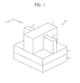
- FIG. 1 is a perspective view of a field effect transistor (FET);
- FIG. 2 is a detailed perspective view of a FET
- FIG. 3 is a perspective view of a silicide at a first end of the gate in the FET illustrated in FIG. 2 ;
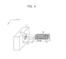
- FIG. 4 is a perspective view of the silicide at a second end of the gate in the FET illustrated in FIG. 2 ;
- FIG. 5 is a cross-sectional view of silicide and contact layers viewed from the first end of the gate in the FET illustrated in FIG. 2 ;
- FIG. 6 is a cross-sectional view of silicide and contact layers viewed from the second end of the gate in the FET illustrated in FIG. 2 ;
- FIG. 7 is a graph showing gate-silicide capacitance and source/drain surface resistance with respect to the silicide length in a unit transistor
- FIG. 8 is a circuit diagram of parasitic capacitance and resistance in a bit cell array including a unit transistor
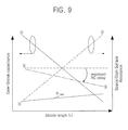
- FIG. 9 is a graph showing gate-silicide capacitance, source/drain surface resistance, and resistance-capacitance (RC) delay with respect to the silicide length in the unit transistor of the bit cell array illustrated in FIG. 8 ;
- FIG. 10 is a circuit diagram of a unit transistor
- FIG. 11 is the voltage-current graph of a pass transistor illustrated in FIG. 10 ;
- FIG. 12 is a graph of current versus current according to a pass transistor and a drive transistor in a static random access memory (SRAM) bit cell manufactured using a planar process in a comparison example;
- SRAM static random access memory
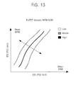
- FIG. 13 is a graph of current versus current according to a pass transistor and a drive transistor in an SRAM bit cell including a FET in a comparison example;
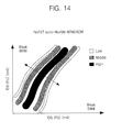
- FIG. 14 is a graph of current versus current according to a pass transistor and a drive transistor in an SRAM bit cell including a FET;
- FIG. 15 is a circuit diagram of a 6-transistor (6T) memory cell
- FIG. 16 is a circuit diagram of an 8-transistor (8T) memory cell
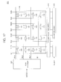
- FIG. 17 is a block diagram of a memory device including a transistor
- FIG. 18 is a block diagram of a memory system including the memory device illustrated in FIG. 17 ;
- FIG. 19 is a block diagram of another memory system including the memory device illustrated in FIG. 17 ;
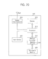
- FIG. 20 is a block diagram of a mobile device including the memory device illustrated in FIG. 17 ;
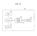
- FIG. 21 is a block diagram of an electronic system including the memory device illustrated in FIG. 17 ;
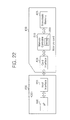
- FIG. 22 is a block diagram of memory card including the memory device illustrated in FIG. 17 ;
- FIG. 23 is a block diagram of an imaging system including the memory device illustrated in FIG. 17 ;
- FIG. 24 is a block diagram of another memory system including the memory device illustrated in FIG. 17 ;
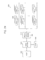
- FIG. 25 is a block diagram of a system-on-chip (SoC) including the memory device illustrated in FIG. 17 .
- SoC system-on-chip
- Example embodiments of the invention are described herein with reference to cross-sectional illustrations that are schematic illustrations of idealized embodiments and intermediate structures of example embodiments. As such, variations from the shapes of the illustrations as a result, for example, of manufacturing techniques and/or tolerances, are to be expected. Thus, example embodiments of the invention should not be construed as limited to the particular shapes illustrated herein but include deviations in shapes that result, for example, from manufacturing.
- FIG. 1 illustrates a field effect transistor (FET) 10 which includes a substrate 5, an insulating layer 4, a source 2, a drain 3, and a gate 1.
- the insulating layer 4 is formed on the substrate 5 (e.g., a Si substrate) and the FET 10 is formed on the insulating layer 4 (e.g., a SiO 2 layer).
- the FET 10 usually includes a fin (between the source 2 and the drain 3) formed of silicon or other semiconductor material and the gate 1 formed of polysilicon or other semiconductor material to cover the fin.
- a channel is formed at a part of the fin extending below the gate 1 between the source and region drain.
- the FET 10 has a double-gate structure surrounding the channel.
- FIG. 2 illustrates the FET 10 according to corresponding embodiments of the invention.
- the FET 10 includes the gate 1, the source 2, the drain 3, silicide layers 6a and 6b, one or more contact layers 7a, 7b, 8a, and 8b, and one or more metal lines 9a and 9b.
- the FET 10 may be implemented in a fin structure formed by etching a semiconductor substrate to form silicon fins, filling a space (or a trench) between adjacent silicon fins with insulating material to electrically isolate the adjacent silicon fins from each other, and exposing a side wall of the silicon fins.
- the gate 1 is between the source 2 and the drain 3 and the silicide layers 6a and 6b, the contact layers 7a, 7b, 8a, and 8b, and the metal lines 9a and 9b are separated from the gate 1.
- the contact layers 7a, 7b, 8a, and 8b are stacked to connect the source 2 and the drain 3 to the metal lines 9a and 9b, respectively.
- the contact layers 7a, 7b, 8a, and 8b electrically connect the source 2 and the drain 3 with the metal lines 9a and 9b, respectively.
- the silicide layers 6a and 6b are between the contact layers 7a and 7b and the upper surfaces of the source 2 and the drain 3, respectively, to decrease the surface resistance of the source 2 and the drain 3 relative and adjust the heights of the source 2 and the drain 3 to the height of the gate 1.
- the FET 10 with the fin structure may have parasitic capacitance between each of the layers (i.e., silicide and contact) and the gate 1.
- the alternating current (AC) performance of the FET 10 may degraded due to the parasitic capacitance.
- the parasitic capacitance between each of the layers and the gate 1 is given by Equation 1: D ⁇ 1 ⁇ ⁇ where C is the respective parasitic capacitance, A1 is an area of a layer facing the gate 1, D1 is a distance between the layer and the gate 1, and ⁇ is a dielectric constant.
- the area A1 of the layer (e.g., a contact or silicide layer) facing the gate 1 may be reduced or the distance between the layers and the gate 1 may be increased. Alternatively, both the area and the distance may be adjusted.
- the distance is an average distance from the face of the layer to the gate.
- the degradation due to parasitic capacitance is reduced by adjusting the aspect ratio of the silicide layers 6a and 6b at the respective two sides of the gate 1 in the FET 10.
- the aspect ratio of the first silicide layer 6a at the side of the source 2 may be adjusted so that the first silicide layer 6a and the second silicide layer 6b at the side of the drain 3 are asymmetric in the FET 10.
- the aspect ratio of the second silicide layer 6b at the side of the drain 3 may be adjusted so that the first silicide layer 6a at the side of the source 2 and the second silicide layer 6b are asymmetric in the FET 10.
- the aspect ratio of both the first and second silicide layers 6a and 6b is adjusted so that the first and second silicide layers 6a and 6b are asymmetric.
- FIG. 3 is a perspective view of the gate 1 and the silicide layer 6a at a first end of the gate 1 in the FET 10 illustrated in FIG. 2 .
- FIG. 4 is a perspective view of the gate 1 and the silicide layer 6b at a second end of the gate 1 in the FET 10 illustrated in FIG. 2 .
- FIG. 5 is a cross-sectional view of the silicide layer 6a and the contact layers 7a and 8a viewed from the first end of the gate 1 in the FET 10 illustrated in FIG. 2 .
- FIG. 6 is a cross-sectional view of the silicide layer 6b and the contact layers 7b and 8b viewed from the second end of the gate 1 in the FET 10 illustrated in FIG. 2 . It is assumed that the aspect ratio of the second silicide layer 6b at the side of the drain 3 is adjusted so that the first silicide layer 6a and the second silicide layer 6b are asymmetric in the FET 10.
- the aspect ratio of the first silicide layer 6a is not adjusted and the surface of the first silicide layer 6a facing the gate has an area of A1 with respect to the gate 1 and is separated from the gate 1 by a distance of D1.
- the aspect ratio of the surface 60 of the second silicide layer 6b is adjusted and the second silicide layer 6b has an area of B1 with respect to the gate 1 and is separated from the gate 1 by the distance D1.
- the area A1 is larger than the area B1.
- the lateral and longitudinal lengths of the surface 50 of the first silicide layer 6a are L1 and L2, respectively, the lateral length L1 of the area B1 of the surface 60 of the second silicide layer 6b is reduced to L3 so that the areas A1 and B1 are different from each other, i.e., asymmetric.
- the length L2 of the first and second silicide layers 6a and 6b may be not adjusted because may affect the height between the contact layers 7a and 8a or 7b and 8b and the source or drain 2 or 3.
- the invention is not restricted to the embodiments discussed so far.
- the aspect ratio of each of the surface of the silicide layers 6a and 6b facing both sides of the gate 1 may be adjusted in the FET 10, so that the degradation due to parasitic capacitance may be reduced.
- the first and second silicide layers 6a and 6b may be arranged asymmetrically around the gate 1 by adjusting the aspect ratio of the surface 50 of the first silicide layer 6a at the side of the source 2 in the FET 10.
- first and second silicide layers 6a and 6b may be arranged asymmetrically around the gate 1 by adjusting both the aspect ratio of the surface 50 of the first silicide layer 6a at the side of the source 2 and the aspect ratio of the surface 60 of the second silicide layer 6b at the side of the drain 3 in the FET 10.
- FIG. 7 is a graph showing gate-silicide capacitance and source/drain surface resistance with respect to a silicide length L in a unit transistor according to some embodiments of the inventive concept.
- the gate-silicide capacitance decreases linearly.
- the surface resistance R is inversely proportional to the area A1 of the silicide facing the gate 1 and is proportional to the distance D1 between the gate 1 and the silicide. Accordingly, when the area of the silicide is decreased from A1 to B1 by adjusting the lateral length of the silicide, the source/drain surface resistance increases.
- FIG. 8 is a circuit diagram of parasitic capacitance and resistance in a bit cell array including a unit transistor, i.e., the FET 10 according to corresponding embodiments of the invention.
- FIG. 9 is a graph showing gate-silicide capacitance, source/drain surface resistance, and resistance-capacitance (RC) delay with respect to the silicide length L in the FET 10 of the bit cell array illustrated in FIG. 8 .
- RC resistance-capacitance
- R sd denotes source-drain parasitic capacitance
- R ch denotes parasitic resistance occurring in a channel of the FET 10
- R TS denotes gate-silicide resistance
- C TS denotes gate-silicide capacitance
- R CA and Rso denote gate-contact resistance
- C CA and C S0 denote gate-contact capacitance
- C S1 and R S1 respectively denote gate-metal capacitance and gate-metal resistance.
- the total resistance R Total is substantially influenced by the gate-silicide resistance R TS .
- a plurality of gate-silicide capacitances C TS are connected in parallel.
- FIG. 10 is a circuit diagram of a unit transistor according to the invention.
- FIG. 11 is the voltage-current graph of a pass transistor illustrated in FIG. 10 .
- the bit cell when a bit cell including the FET 10 is modeled, the bit cell includes a total resistance R Total , a pass transistor TR PASS , and a drive transistor TR Drive .
- the pass transistor TR PASS and the drive transistor TR Drive are turned on. According to the operation, a source-drain direction is determined as shown in Table 1.
- the pass transistor TR PASS has a node Q1 as a source and a node Q2 as a drain.
- a drain voltage drops due to the total resistance R Total an d a drain-source voltage V DS decreases.
- a read current I read flows from the node Q2 to the node Q1.
- the pass transistor TR PASS is in a saturation area since a gate-source voltage hardly changes (6) even through the drain-source voltage V DS decreases (8 ⁇ 9), as shown in FIG. 11 .
- the decrement in the read current I DS is very slight.
- the current flows in an opposite direction to program data to the FET 10, so the node Q1 becomes a drain and the node Q2 becomes a source.
- a source voltage drops due to the total resistance R Total and the gate-source voltage V GS decreases (6 ⁇ 7).
- the decrement in the write current I DS may occur due to the total resistance R Total , as shown in FIG. 11 .
- the decrease in write current has a very limited affect on the overall write operation speed of the memory device.
- FIG. 12 is a graph of current versus current according to a pass transistor and a drive transistor in a static random access memory (SRAM) bit cell manufactured using a planar process in a comparison example.
- FIG. 13 is a graph of current versus current according to a pass transistor and a drive transistor in an SRAM bit cell including an FET in a comparison example.
- FIG. 14 is a graph of current versus current according to a pass transistor and a drive transistor in an SRAM bit cell including an FET according to the invention.
- SRAM static random access memory
- a static noise margin (SNM) (or a read margin) and a writability margin (WRM) have dispositions toward opposite directions, respectively.
- SNM static noise margin
- WRM writability margin
- a bit cell yield is highest when the strength of the pass transistor is similar to that of the drive transistor according to the threshold voltage of each transistor, the effective width of a fin, and the length of the fin.
- SNM read stability
- WRM write stability
- bit cell yield depending on the strength of each transistor has a discrete distribution.
- bit cell stability i.e., WRM and SNM
- WRM and SNM bit cell stability
- bit cell stability i.e., WRM and SNM
- WRM and SNM can be tuned in a wider range in processes.
- FIG. 15 is a circuit diagram of a 6-transistor (6T) memory cell 100.
- FIG. 16 is a circuit diagram of an 8-transistor (8T) memory cell 100'.
- the memory cell 100 includes two cross-coupled inverters formed by electrically connecting a first pull-up transistor 105, a first pull-down transistor 109, a second pull-up transistor 107, and a second pull-down transistor 111 with one another. Drains of the first pull-down transistor 109 and the first pull-up transistor 105 are electrically connected with gates of the second pull-up transistor 107 and the second pull-down transistor 111. Drains of the second pull-up transistor 107 and the second pull-down transistor 111 are electrically connected with gates of the first pull-up transistor 105 and the first pull-down transistor 109.
- the memory cell (e.g., SRAM cell) 100 also includes a first pass-gate transistor 101 and a second pass-gate transistor 115.
- Pass-gate transistors such as the first pass-gate transistor 101 and the second pass-gate transistor 115 may have a longer gate length than pull-down devices such as the first pull-down transistor 109 and the second pull-down transistor 111.
- Gates of the pass-gate transistors 101 and 115 are connected to a word line WL that controls an access to read data from or write data to the memory cell 100.
- the first pass-gate transistor 101 is connected to a bit line BL and the second pass-gate transistor 115 is connected to a complementary bit line BLB.
- the first pass-gate transistor 101 is connected to a common node between the first pull-down transistor 109 and the first pull-up transistor 105.
- the second pass-gate transistor 115 is connected to a common node between the second pull-down transistor 111 and the second pull-up transistor 107.
- data is written into the memory cell 100 by turning on the first pass-gate transistor 101 and the second pass-gate transistor 115 by applying a high voltage to the word line WL.
- the pass-gate transistors 101 and 115 are turned on, both the bit line BL and the complementary bit line BLB may be used to write data to the memory cell 100.
- the memory cell 100' illustrated in FIG. 16 further includes a read buffer 200.
- the memory cell 100' including 8 transistors provides individual read and write paths for a bit of data that has been stored.
- the read buffer 200 includes a read pass-gate transistor 203 and a read drive transistor 201.
- the read pass-gate transistor 203 and the read drive transistor 201 are connected in series between a read bit line RBL and a ground voltage.
- the read pass-gate transistor 203 is gated by a read word line RWL and individually reads a data cell according to the read bit line RBL.
- a gate of the read drive transistor 201 is connected to the gate of the second pull-up transistor 107 to generate a read current from the data cell.
- FIG. 17 is a block diagram of a memory device 300 including a transistor according to the invention.
- the memory device 300 includes a column selection switch 310, a column decoder 320, a row decoder 330, and a bit cell array 350.
- the bit cell array 350 includes a plurality of bit cells 100.
- Each bit cell 100 may be implemented by an SRAM cell including the FET 10, as shown in FIG. 15 or 16 .
- the row decoder 330 decodes a row address XADDR and enables a word line WL corresponding to it.
- the column decoder 320 decodes a column address YADDR and enables bit lines BL and BLB corresponding to it.
- the column selection switch 310 switches the enabled bit lines BL and BLB. Although there are four word lines WL1 through WL4 and four bit lines BL1 through BL4 and BLB1 through BLB4 in FIG. 17 , the inventive concept is not so restricted.
- FIG. 18 is a block diagram of a memory system 400 including the memory device 300 illustrated in FIG. 17 according to the invention.
- the memory system 400 includes a non-volatile memory device 450, the memory device 300, and a central processing unit (CPU) 410 controlling the operations of the memory device 300 and the non-volatile memory device 450.
- the CPU 410 may be a microprocessor.
- the memory device 300 may be used as an operating memory of the CPU 410.
- the memory device 300 may be implemented by SRAM.
- a host connected to the memory system 400 may perform data communication with the non-volatile memory device 450 through a memory interface (I/F) 420 and a host I/F 440.
- I/F memory interface
- an error correction code (ECC) block 430 may detect an error in data received from the non-volatile memory device 450 through the memory I/F 420, correct the bit in error, and transmit the corrected data to the host through the host I/F 440.
- the CPU 410 may control data communication among the memory I/F 420, the ECC block 430, the host I/F 440, and the volatile memory device 300 via a bus 401.
- the memory system 400 may be implemented as a flash memory drive, a universal serial bus (USB) flash memory drive, an inter-chip USB (IC-USB) memory drive, or a memory stick. Other implementations are also within the scope of the invention.
- USB universal serial bus
- IC-USB inter-chip USB
- FIG. 19 is a block diagram of a memory system 500 including the memory device 300 illustrated in FIG. 17 according to the invention.
- the memory system 500 includes an input unit 510, a controller 520, a non-volatile memory device 530, a memory controller 540 including the SRAM 300, a dynamic RAM (DRAM) controller 550, a DRAM 560, and an output unit 570.
- DRAM dynamic RAM
- the input unit 510 can receive an external command.
- the controller 520 generates a control signal for executing the command received through the input unit 510.
- data stored in the non-volatile memory device 530 is transmitted to the memory controller 540 and stored in the SRAM 300 included in the memory controller 540.
- the memory controller 540 stores data from the non-volatile memory device 530 in the SRAM 300 functioning as a buffer memory before transmitting the data to the DRAM 560, thereby conducting delay that may occur when directly storing the data output from the non-volatile memory device 530 in the DRAM 560.
- the DRAM controller 550 stores data output from the SRAM 300 in the DRAM 560.
- the data stored in the DRAM 560 may be output through the output unit 570 according to the control of the controller 520.
- FIG. 20 is a block diagram of a mobile device 600 including the memory device 300 illustrated in FIG. 17 according to the invention.
- the mobile device 600 may be implemented as a cellular phone, a smart phone, a tablet personal computer (PC), a personal digital assistant (PDA) or a radio communication system.
- PC personal computer
- PDA personal digital assistant
- the mobile device 600 includes the non-volatile memory device 660 and a memory controller 650 controlling the operations of the non-volatile memory device 660.
- the memory controller 650 may control the data access operations, e.g., program operations, erase operations, and read operations, of the non-volatile memory device 660 according to the control of a processor 610.
- the memory controller 650 includes the SRAM 300 for storing the data output from the non-volatile memory device 660.
- the SRAM 300 temporarily stores the data output from the non-volatile memory device 660.
- the data stored in the SRAM 300 may be transmitted to the processor 610.
- a radio transceiver 630 transmits or receives radio signals through an antenna ANT.
- the radio transceiver 630 may convert radio signals received through the antenna ANT into signals that can be processed by the processor 610. Accordingly, the processor 610 may process the signals output from the radio transceiver 630 and transmit the processed signals to the memory controller 650 or the display 620.
- the memory controller 650 may program the signals processed by the processor 610 to the non-volatile memory device 660.
- the radio transceiver 630 may also convert signals output from the processor 610 into radio signals and transmit the radio signals to an external device via the antenna ANT.
- An input device 640 enables control signals for controlling the operation of the processor 610 or data to be processed by the processor 610 to be input to the mobile device 600.
- the input device 640 may be implemented by a pointing device such as a touch pad or a computer mouse, a keypad, or a keyboard.
- the processor 610 may control the operation of the display 620 to display data output from the memory controller 650, data output from the radio transceiver 630, or data output from the input device 640.
- the memory controller 650 which controls the operations of the non-volatile memory device 660, may be implemented as a part of the processor 610 or as a separate chip.
- the memory controller 650 and the non-volatile memory device 660 may be implemented as single package, for example, a multi-chip package
- FIG. 21 is a block diagram of an electronic system 700 including the memory device 300 illustrated in FIG. 17 according to another embodiment of the invention.
- the electronic system 700 may be implemented as a personal computer (PC), a tablet PC, a netbook, an e-reader, a personal digital assistant (PDA), a portable multimedia player (PMP), an MP3 player, an MP4 player or the like.
- PC personal computer
- PDA personal digital assistant
- PMP portable multimedia player
- MP3 player MP3 player
- MP4 player MP4 player
- the electronic system 700 includes the non-volatile memory device 750 and a memory controller 740 controlling the data processing operations of the non-volatile memory device 750.
- the memory controller 740 includes the SRAM 300.
- the memory controller 740 temporarily stores data output from the non-volatile memory device 750 in the SRAM 300.
- the data stored in the SRAM 300 may be transmitted to a processor 710.
- the processor 710 may display data stored in the non-volatile memory device 750 through a display 730 according to data input through an input device 720.
- the input device 720 may be implemented by a pointing device such as a touch pad or a computer mouse, a keypad, or a keyboard.
- the processor 710 may control the overall operation of the electronic system 700 and the operations of the memory controller 740.
- the memory controller 740 which may control the operations of the non-volatile memory device 750, may be implemented as a part of the processor 710 or as a separate chip.
- the memory controller 740 and the non-volatile memory device 750 may be implemented as single package, for example, a multi-chip package
- FIG. 22 is a block diagram of a memory card 800 including the memory device 300 illustrated in FIG. 17 according to the invention.
- the memory card 800 may be implemented as any type of memory card, such as a smart card.
- the memory card 800 includes the non-volatile memory device 805, a memory controller 810, and a card interface 820.
- the memory controller 810 may control data exchange between the non-volatile memory device 805 and the card interface 820.
- the card interface 820 may be a secure digital (SD) card interface or a multi-media card (MMC) interface, but the inventive concept is not so restricted.
- the card interface 820 may interface to a host 830 and the memory controller 810 for data exchange according to a protocol of the host 830.
- the memory controller 810 temporarily stores data output from the non-volatile memory device 805 in the SRAM 300.
- the data stored in the SRAM 300 may be transmitted to the card interface 820.
- the card interface 820 may support a universal serial bus (USB) protocol, an interchip (IC)-USB protocol or other protocols.
- USB universal serial bus
- IC interchip
- the card interface 820 may indicate a hardware supporting a protocol used by the host 830, a software installed in the hardware, or a signal transmission mode.
- a host interface 850 of the host 830 may perform data communication with the non-volatile memory device 805 through the card interface 820 and the memory controller 810 according to the control of a microprocessor 840 (other processors may be used).
- FIG. 23 is a block diagram of an imaging system 900 including the memory device 300 illustrated in FIG. 17 according to the invention.
- the imaging system 900 may be implemented as an image processor included in a digital camera, a cellular phone equipped with a digital camera, a smart phone equipped with a digital camera, a tablet PC equipped with a digital camera, or in some other electronic device.
- the imaging system 900 includes the non-volatile memory device 980 and a memory controller 970 controlling the data processing operations, such as program operations, erase operations, and read operations, of the non-volatile memory device 980.
- the memory controller 970 includes the SRAM 300 for temporarily storing data output from the non-volatile memory device 980 or data to be output to the non-volatile memory device 980.
- An image sensor 920 included in the imaging system 900 converts optical images into digital signals and outputs the digital signals to a processor 910 or the memory controller 970.
- the digital signals may be controlled by the processor 910 to be displayed through a display 930 or stored in the non-volatile memory device 980 through the memory controller 970.
- Data stored in the non-volatile memory device 980 may be displayed through the display 930 according to the control of the processor 910 or the memory controller 970.
- the memory controller 970 which may control the operations of the non-volatile memory device 980, may be implemented as a part of the processor 910 or as a separate chip.
- FIG. 24 is a block diagram of a memory system 1000 including the memory device 300 illustrated in FIG. 17 according to the invention.
- the memory system 1000 may be implemented as a data storage system like a solid state drive (SSD).
- SSD solid state drive
- the memory system 1000 includes a plurality of non-volatile memory devices 1050 (such as NAND devices), a memory controller 1010 controlling the data processing operations of the non-volatile memory devices 1050, a dynamic random access memory (DRAM) 1030, and a buffer manager 1020 controlling data transferred between the memory controller 1010 and a host 1040 to be stored in the DRAM 1030.
- non-volatile memory devices 1050 such as NAND devices
- memory controller 1010 controlling the data processing operations of the non-volatile memory devices 1050
- DRAM dynamic random access memory
- buffer manager 1020 controlling data transferred between the memory controller 1010 and a host 1040 to be stored in the DRAM 1030.
- the memory controller 1010 includes the SRAM 300.
- the SRAM 300 may temporarily store data output from the non-volatile memory device 1050 and transmit the data to the DRAM 1030 according to the control of the buffer manager 1020.
- FIG. 25 is a block diagram of a system-on-chip (SoC) 1100 including the memory device 300 illustrated in FIG. 17 according to the invention.
- the SoC 1100 includes a CPU 1101, the memory device 300, an I/F 1102, a graphics processing unit (GPU) 1103, a display controller 1104, and an external memory controller 1105.
- the CPU 1101 which controls the overall operation of the SoC 1100 may control the operations of the elements 300, 1102, 1103, 1104, and 1105.
- the external memory controller 1105 may control the operations when transmitting data to and receiving data from an external memory 1130 connected to the SoC 1100.
- GPU 1103 processes data that the memory controller 1105 has read from the external memory 1130 to provide signals suitable for display.
- the display controller 1104 controls whether to transmit the processed signal to a display device 1120.
- the aspect ratio of a silicide layer on a source/drain is adjusted to reduce a total capacitance in a FET, thereby increasing the read and write stability of a memory device.
Landscapes
- Engineering & Computer Science (AREA)
- Microelectronics & Electronic Packaging (AREA)
- Computer Hardware Design (AREA)
- Semiconductor Memories (AREA)
- Thin Film Transistor (AREA)
- Electrodes Of Semiconductors (AREA)
- Metal-Oxide And Bipolar Metal-Oxide Semiconductor Integrated Circuits (AREA)
Abstract
Description
- The invention relates to a field effect transistor (FET) and a fin field effect transistor (FET) arrangement and to related devices such as a memory device, a memory cell array, a memory controller, a memory system, a memory card, a solid state drive, and a system-on-chip (SoC).
- As FETs becomes smaller and the manufacturing processes thereof more segmented, the complexity of related transistor contacts may become an issue. As such contacts become more complicated, parasitic capacitance associated with those contacts may be a problem.
- It is the technical problem of the invention to provide a field effect transistor, a finFET arrangement and related devices which are capable to reduce or avoid the difficulties of the prior art mentioned above.
- The invention solves this problem by providing a field effect transistor having the features of claim1, a finFET arrangement having the features of
claim 4, a memory device having the features of claim 7, a memory controller having the features of claim 12, a memory system having the features of claim 14, a memory card having the features of claim 15, a solid state drive having the features of claim 16, a system-on-chip having the features of claim 17, and a memory cell array having the features of claim 18. Advantageous embodiments of the invention are mentioned in the dependent claims the wording of which is herewith incorporated into the description by reference to avoid unnecessary text repetition. - Embodiments according to the invention may provide FETs including asymmetrical silicide structures and related devices. Pursuant to these embodiments, in some embodiments of the inventive concept, a field effect transistor can include a first silicide layer on a source of the FET where the first silicide layer can be separated from a gate of the FET. A second silicide layer can be on a drain of the FET and the second silicide layer can be separated from the gate and at least one contact layer can be on each of the first and second silicide layers. An aspect ratio of at least one of the first and second silicide layers can be adjusted so that the first and second silicide layers are asymmetric to one another.
- In corresponding embodiments according to the invention, a memory device can include a memory cell array that includes a plurality of memory cells. A peripheral circuit can be configured to access the memory cells, where each of the memory cells can include a plurality of field effect transistors. The field effect transistors can include a first silicide layer on a source of the FET, where the first silicide layer can be separated from a gate of the FET. A second silicide layer can be on a drain of the FET, where the second silicide layer can be separated from the gate and have an area with respect to the gate, which has an asymmetric relation with an area of the first silicide layer with respect to the gate. At least one contact can be positioned on each of the first and second silicide layers.
In corresponding embodiments according to the invention, a memory controller can include a memory device and a microprocessor that can be configured to control operation of the memory device. The memory device can include a memory cell array with a plurality of memory cells each of which each can include a plurality of field effect transistors, an access control circuit that can be configured to access the memory cell array to perform a read operation or a write operation, and a control signal generation circuit that can be configured to generate a control signal for controlling an operation of the access control circuit. - In corresponding embodiments according to the invention, an system-on-chip (SoC) can include a central processing unit (CPU), a memory controller that can be configured to access an external memory to read or write data according to the control of the CPU, and a memory device that can be configured to store the data to be read or written according to the control of the CPU. The memory device can include a memory cell array including a plurality of memory cells and a peripheral circuit that can be configured to access the memory cells.
- Each of the memory cells can include a plurality of field effect transistors. Each of the field effect transistors can include a first silicide layer positioned on a source and separated from a gate. A second silicide layer can be positioned on a drain and separated from the gate, the second silicide layer can have an area with respect to the gate which has an asymmetric relation with an area of the first silicide layer with respect to the gate. At least one contact can be positioned on each of the first and second silicide layers.
- In corresponding embodiments, a fin Field Effect Transistor (finFET) can include a source region and a drain region of the finFET. A gate of the finFET can cross over a fin of the finFET between the source and drain regions. First and second silicide layers can be on the source and drain regions respectively. The first and second silicide layers can include respective first and second surfaces that face the gate crossing over the fin, where the first and second surfaces are different sizes.
- Advantageous embodiments of the invention are described in the following and shown in the attached drawings in which:
-
FIG. 1 is a perspective view of a field effect transistor (FET); -
FIG. 2 is a detailed perspective view of a FET; -
FIG. 3 is a perspective view of a silicide at a first end of the gate in the FET illustrated inFIG. 2 ; -
FIG. 4 is a perspective view of the silicide at a second end of the gate in the FET illustrated inFIG. 2 ; -
FIG. 5 is a cross-sectional view of silicide and contact layers viewed from the first end of the gate in the FET illustrated inFIG. 2 ; -
FIG. 6 is a cross-sectional view of silicide and contact layers viewed from the second end of the gate in the FET illustrated inFIG. 2 ; -
FIG. 7 is a graph showing gate-silicide capacitance and source/drain surface resistance with respect to the silicide length in a unit transistor; -
FIG. 8 is a circuit diagram of parasitic capacitance and resistance in a bit cell array including a unit transistor; -
FIG. 9 is a graph showing gate-silicide capacitance, source/drain surface resistance, and resistance-capacitance (RC) delay with respect to the silicide length in the unit transistor of the bit cell array illustrated inFIG. 8 ; -
FIG. 10 is a circuit diagram of a unit transistor; -
FIG. 11 is the voltage-current graph of a pass transistor illustrated inFIG. 10 ; -
FIG. 12 is a graph of current versus current according to a pass transistor and a drive transistor in a static random access memory (SRAM) bit cell manufactured using a planar process in a comparison example; -
FIG. 13 is a graph of current versus current according to a pass transistor and a drive transistor in an SRAM bit cell including a FET in a comparison example; -
FIG. 14 is a graph of current versus current according to a pass transistor and a drive transistor in an SRAM bit cell including a FET; -
FIG. 15 is a circuit diagram of a 6-transistor (6T) memory cell; -
FIG. 16 is a circuit diagram of an 8-transistor (8T) memory cell; -
FIG. 17 is a block diagram of a memory device including a transistor; -
FIG. 18 is a block diagram of a memory system including the memory device illustrated inFIG. 17 ; -
FIG. 19 is a block diagram of another memory system including the memory device illustrated inFIG. 17 ; -
FIG. 20 is a block diagram of a mobile device including the memory device illustrated inFIG. 17 ; -
FIG. 21 is a block diagram of an electronic system including the memory device illustrated inFIG. 17 ; -
FIG. 22 is a block diagram of memory card including the memory device illustrated inFIG. 17 ; -
FIG. 23 is a block diagram of an imaging system including the memory device illustrated inFIG. 17 ; -
FIG. 24 is a block diagram of another memory system including the memory device illustrated inFIG. 17 ; and -
FIG. 25 is a block diagram of a system-on-chip (SoC) including the memory device illustrated inFIG. 17 . - Example embodiments of the invention are described herein with reference to cross-sectional illustrations that are schematic illustrations of idealized embodiments and intermediate structures of example embodiments. As such, variations from the shapes of the illustrations as a result, for example, of manufacturing techniques and/or tolerances, are to be expected. Thus, example embodiments of the invention should not be construed as limited to the particular shapes illustrated herein but include deviations in shapes that result, for example, from manufacturing.
- It will be understood that when an element is referred to as being "coupled," "connected," or "responsive" to, or "on," another element, it can be directly coupled, connected, or responsive to, or on, the other element, or intervening elements may also be present. In contrast, when an element is referred to as being "directly coupled," "directly connected," or "directly responsive" to, or "directly on," another element, there are no intervening elements present. As used herein the term "and/or" includes any and all combinations of one or more of the associated listed items.
-
FIG. 1 illustrates a field effect transistor (FET) 10 which includes asubstrate 5, aninsulating layer 4, asource 2, adrain 3, and agate 1. Theinsulating layer 4 is formed on the substrate 5 (e.g., a Si substrate) and theFET 10 is formed on the insulating layer 4 (e.g., a SiO2 layer). The FET 10 usually includes a fin (between thesource 2 and the drain 3) formed of silicon or other semiconductor material and thegate 1 formed of polysilicon or other semiconductor material to cover the fin. A channel is formed at a part of the fin extending below thegate 1 between the source and region drain. The FET 10 has a double-gate structure surrounding the channel. -
FIG. 2 illustrates theFET 10 according to corresponding embodiments of the invention. Referring toFIG. 2 , theFET 10 includes thegate 1, thesource 2, thedrain 3,silicide layers more contact layers more metal lines - The
FET 10 may be implemented in a fin structure formed by etching a semiconductor substrate to form silicon fins, filling a space (or a trench) between adjacent silicon fins with insulating material to electrically isolate the adjacent silicon fins from each other, and exposing a side wall of the silicon fins. In other words, thegate 1 is between thesource 2 and thedrain 3 and the silicide layers 6a and 6b, thecontact layers metal lines gate 1. - The contact layers 7a, 7b, 8a, and 8b are stacked to connect the
source 2 and thedrain 3 to themetal lines contact layers source 2 and thedrain 3 with themetal lines - The silicide layers 6a and 6b are between the contact layers 7a and 7b and the upper surfaces of the
source 2 and thedrain 3, respectively, to decrease the surface resistance of thesource 2 and thedrain 3 relative and adjust the heights of thesource 2 and thedrain 3 to the height of thegate 1. - The
FET 10 with the fin structure may have parasitic capacitance between each of the layers (i.e., silicide and contact) and thegate 1. When a signal generated in thesource 2 and/or thedrain 3 is transmitted to themetal lines FET 10 may degraded due to the parasitic capacitance. As appreciated by the present inventors, the less the parasitic capacitance associated with the layers, the higher the performance of theFET 10 may be. The parasitic capacitance between each of the layers and thegate 1 is given by Equation 1:
where C is the respective parasitic capacitance, A1 is an area of a layer facing thegate 1, D1 is a distance between the layer and thegate 1, and ε is a dielectric constant. In other words, in order to reduce the parasitic capacitance C, the area A1 of the layer (e.g., a contact or silicide layer) facing thegate 1 may be reduced or the distance between the layers and thegate 1 may be increased. Alternatively, both the area and the distance may be adjusted. In some embodiments, the distance is an average distance from the face of the layer to the gate. - According to the invention, the degradation due to parasitic capacitance is reduced by adjusting the aspect ratio of the silicide layers 6a and 6b at the respective two sides of the
gate 1 in theFET 10. In corresponding embodiments, the aspect ratio of thefirst silicide layer 6a at the side of thesource 2 may be adjusted so that thefirst silicide layer 6a and thesecond silicide layer 6b at the side of thedrain 3 are asymmetric in theFET 10. In corresponding embodiments, the aspect ratio of thesecond silicide layer 6b at the side of thedrain 3 may be adjusted so that thefirst silicide layer 6a at the side of thesource 2 and thesecond silicide layer 6b are asymmetric in theFET 10. In corresponding embodiments, the aspect ratio of both the first andsecond silicide layers second silicide layers -
FIG. 3 is a perspective view of thegate 1 and thesilicide layer 6a at a first end of thegate 1 in theFET 10 illustrated inFIG. 2 .FIG. 4 is a perspective view of thegate 1 and thesilicide layer 6b at a second end of thegate 1 in theFET 10 illustrated inFIG. 2 .FIG. 5 is a cross-sectional view of thesilicide layer 6a and the contact layers 7a and 8a viewed from the first end of thegate 1 in theFET 10 illustrated inFIG. 2 .FIG. 6 is a cross-sectional view of thesilicide layer 6b and the contact layers 7b and 8b viewed from the second end of thegate 1 in theFET 10 illustrated inFIG. 2 . It is assumed that the aspect ratio of thesecond silicide layer 6b at the side of thedrain 3 is adjusted so that thefirst silicide layer 6a and thesecond silicide layer 6b are asymmetric in theFET 10. - Referring to
FIGS. 3 and5 , the aspect ratio of thefirst silicide layer 6a is not adjusted and the surface of thefirst silicide layer 6a facing the gate has an area of A1 with respect to thegate 1 and is separated from thegate 1 by a distance of D1. However, referring toFIGS. 4 and6 , the aspect ratio of thesurface 60 of thesecond silicide layer 6b is adjusted and thesecond silicide layer 6b has an area of B1 with respect to thegate 1 and is separated from thegate 1 by the distance D1. At this time, the area A1 is larger than the area B1. When the lateral and longitudinal lengths of thesurface 50 of thefirst silicide layer 6a are L1 and L2, respectively, the lateral length L1 of the area B1 of thesurface 60 of thesecond silicide layer 6b is reduced to L3 so that the areas A1 and B1 are different from each other, i.e., asymmetric. The length L2 of the first andsecond silicide layers - The invention is not restricted to the embodiments discussed so far. The aspect ratio of each of the surface of the silicide layers 6a and 6b facing both sides of the
gate 1 may be adjusted in theFET 10, so that the degradation due to parasitic capacitance may be reduced. For instance, the first andsecond silicide layers gate 1 by adjusting the aspect ratio of thesurface 50 of thefirst silicide layer 6a at the side of thesource 2 in theFET 10. Alternatively, the first andsecond silicide layers gate 1 by adjusting both the aspect ratio of thesurface 50 of thefirst silicide layer 6a at the side of thesource 2 and the aspect ratio of thesurface 60 of thesecond silicide layer 6b at the side of thedrain 3 in theFET 10. -
FIG. 7 is a graph showing gate-silicide capacitance and source/drain surface resistance with respect to a silicide length L in a unit transistor according to some embodiments of the inventive concept. Referring toFIG. 7 , when the lateral length of a silicide layer is reduced as shown inFIGS. 3 through 6 (L1>L3 at this time) in order to reduce a gate-silicide area (e.g., A1), the gate-silicide capacitance decreases linearly. Meanwhile, the source/drain surface resistance can be obtained using Equation 2:
where R is the surface resistance, p is a resistance coefficient, "1" is the length, and S is the area. - According to
Equation 2, the surface resistance R is inversely proportional to the area A1 of the silicide facing thegate 1 and is proportional to the distance D1 between thegate 1 and the silicide. Accordingly, when the area of the silicide is decreased from A1 to B1 by adjusting the lateral length of the silicide, the source/drain surface resistance increases. - In other words, when the silicide layers 6a and 6b at both sides of the
gate 1 are adjusted to be asymmetric, the gate-silicide capacitance decreases, but the source/drain surface resistance R increases. If this happens in just asingle FET 10, it may not be construed that the AC performance of theFET 10 increases. However, in a case of a bit cell array including a plurality ofFETs 10, the AC performance increases. This will be described in detail with reference toFIGS. 8 through 14 . -
FIG. 8 is a circuit diagram of parasitic capacitance and resistance in a bit cell array including a unit transistor, i.e., theFET 10 according to corresponding embodiments of the invention.FIG. 9 is a graph showing gate-silicide capacitance, source/drain surface resistance, and resistance-capacitance (RC) delay with respect to the silicide length L in theFET 10 of the bit cell array illustrated inFIG. 8 . InFIG. 8 , Rsd denotes source-drain parasitic capacitance, Rch denotes parasitic resistance occurring in a channel of theFET 10, RTS denotes gate-silicide resistance, CTS denotes gate-silicide capacitance, RCA and Rso denote gate-contact resistance, CCA and CS0 denote gate-contact capacitance, and CS1 and RS1 respectively denote gate-metal capacitance and gate-metal resistance. - When parasitic capacitance and parasitic resistance are modeled for the bit cell array, "n" FETs D1 through Dn are connected in parallel to a single bit line, as shown in
FIG. 8 . Even though there are multiple gate-silicide resistances RTS, only one gate-silicide resistances RTS substantially has an effect as shown in a circle E1 due to the parallel connection since a word line activates one FET D1 to read a data bit. A total resistance RTotal is the sum of resistances which have an effect when a single bit line is enabled and is defined as Equation 3:
- Here, since the gate-contact resistances RCA and RS0 and the gate-metal resistance RS1 are fixed, the total resistance RTotal is substantially influenced by the gate-silicide resistance RTS. A plurality of gate-silicide capacitances CTS are connected in parallel. A capacitance CD1 per bit cell is defined based on a serial connection as
Equation 4 and a capacitance CTotal per bit line is defined based on a parallel connection as Equation 5:

- With respect to the capacitance CTotal per bit line, all gate-silicide capacitances CTS in circles E1 through En, which are connected in parallel to a single bit line, substantially have an effect. Since the gate-contact capacitances CCA and CS0 and the gate-metal capacitance CS1 are fixed, the total capacitance CTotal is substantially influenced by the gate-silicide capacitance CTS.
- In a
single FET 10, as shown inFIG. 7 , as the length L of one silicide layer increases, the gate-silicide resistance RTS increases (②) and the gate-silicide capacitance CTS decreases. However, in the entire bit cell array where a plurality ofFETs 10 are connected, even through a total resistance increases as the gate-silicide resistance RTS increases (②), the capacitance CTotal per bit line decreases due to the decrease (①) in the gate-silicide capacitance CTS. As a result, a time constant, i.e., the RC delay decreases (④⇒⑤) in the bit cell array. Accordingly, the entire performance of a memory device including the bit cell array including a plurality ofFETs 10 increases. -
FIG. 10 is a circuit diagram of a unit transistor according to the invention.FIG. 11 is the voltage-current graph of a pass transistor illustrated inFIG. 10 . Referring toFIG. 10 , when a bit cell including theFET 10 is modeled, the bit cell includes a total resistance RTotal, a pass transistor TRPASS, and a drive transistor TRDrive. When a word line is enabled according to an operation on the bit cell, the pass transistor TRPASS and the drive transistor TRDrive are turned on. According to the operation, a source-drain direction is determined as shown in Table 1.Table 1 Operation Source Drain Read Q1 Q2 Write Q2 Q1 - In a read operation, the pass transistor TRPASS has a node Q1 as a source and a node Q2 as a drain. During the read operation, a drain voltage drops due to the total resistance RTotal an d a drain-source voltage VDS decreases. A read current Iread flows from the node Q2 to the node Q1. At this time, the pass transistor TRPASS is in a saturation area since a gate-source voltage hardly changes (⑥) even through the drain-source voltage VDS decreases (⑧⇒⑨), as shown in
FIG. 11 . As a result, the decrement in the read current IDS is very slight. - In a write operation, the current flows in an opposite direction to program data to the
FET 10, so the node Q1 becomes a drain and the node Q2 becomes a source. In this case, a source voltage drops due to the total resistance RTotal and the gate-source voltage VGS decreases (⑥⇒⑦). As a result, the decrement in the write current IDS may occur due to the total resistance RTotal, as shown inFIG. 11 . However, since a strong external drive voltage is applied to the drive transistor TRDrive in the write operation of a memory device using theFET 10, the decrease in write current has a very limited affect on the overall write operation speed of the memory device. -
FIG. 12 is a graph of current versus current according to a pass transistor and a drive transistor in a static random access memory (SRAM) bit cell manufactured using a planar process in a comparison example.FIG. 13 is a graph of current versus current according to a pass transistor and a drive transistor in an SRAM bit cell including an FET in a comparison example.FIG. 14 is a graph of current versus current according to a pass transistor and a drive transistor in an SRAM bit cell including an FET according to the invention. - Referring to
FIG. 12 , according to the strength of the pass transistor and the drive transistor (or a pull-up transistor), a static noise margin (SNM) (or a read margin) and a writability margin (WRM) have dispositions toward opposite directions, respectively. In other words, a bit cell yield is highest when the strength of the pass transistor is similar to that of the drive transistor according to the threshold voltage of each transistor, the effective width of a fin, and the length of the fin. When the pass transistor is stronger than the drive transistor or when the drive transistor is stronger than the pass transistor, the bit cell yield decreases gradually to a middle and a low level and read stability (i.e., SNM) or write stability (i.e., WRM) is weakened. However, when SRAM bit cells are manufactured using the planar process, the bit cell yield has a linear distribution. - Referring to
FIG. 13 , since an area in which a fin FET can adjust the width of a transistor is discrete, the bit cell yield depending on the strength of each transistor has a discrete distribution. When the bit cell yield is discrete, bit cell stability (i.e., WRM and SNM) needs to be tuned in a very limited range in processes. - When a bit cell uses the
FET 10 according to of the invention, resistance and capacitance are adjusted as described above, and therefore, the bit cell yield may have a semi-linear distribution, as shown inFIG. 14 . As a result, bit cell stability (i.e., WRM and SNM) can be tuned in a wider range in processes. -
FIG. 15 is a circuit diagram of a 6-transistor (6T)memory cell 100.FIG. 16 is a circuit diagram of an 8-transistor (8T) memory cell 100'. Referring toFIG. 15 , thememory cell 100 includes two cross-coupled inverters formed by electrically connecting a first pull-uptransistor 105, a first pull-down transistor 109, a second pull-uptransistor 107, and a second pull-down transistor 111 with one another. Drains of the first pull-down transistor 109 and the first pull-uptransistor 105 are electrically connected with gates of the second pull-uptransistor 107 and the second pull-down transistor 111. Drains of the second pull-uptransistor 107 and the second pull-down transistor 111 are electrically connected with gates of the first pull-uptransistor 105 and the first pull-down transistor 109. - The memory cell (e.g., SRAM cell) 100 also includes a first
pass-gate transistor 101 and a secondpass-gate transistor 115. Pass-gate transistors such as the firstpass-gate transistor 101 and the secondpass-gate transistor 115 may have a longer gate length than pull-down devices such as the first pull-down transistor 109 and the second pull-down transistor 111. Gates of thepass-gate transistors memory cell 100. Also, the firstpass-gate transistor 101 is connected to a bit line BL and the secondpass-gate transistor 115 is connected to a complementary bit line BLB. The firstpass-gate transistor 101 is connected to a common node between the first pull-down transistor 109 and the first pull-uptransistor 105. The secondpass-gate transistor 115 is connected to a common node between the second pull-down transistor 111 and the second pull-uptransistor 107. - In the embodiments illustrated in
FIG. 15 , data is written into thememory cell 100 by turning on the firstpass-gate transistor 101 and the secondpass-gate transistor 115 by applying a high voltage to the word line WL. When thepass-gate transistors memory cell 100. - Compared to the
memory cell 100 illustrated inFIG. 15 , the memory cell 100' illustrated inFIG. 16 further includes a readbuffer 200. The memory cell 100' including 8 transistors provides individual read and write paths for a bit of data that has been stored. The readbuffer 200 includes a readpass-gate transistor 203 and aread drive transistor 201. Theread pass-gate transistor 203 and theread drive transistor 201 are connected in series between a read bit line RBL and a ground voltage. Theread pass-gate transistor 203 is gated by a read word line RWL and individually reads a data cell according to the read bit line RBL. A gate of theread drive transistor 201 is connected to the gate of the second pull-uptransistor 107 to generate a read current from the data cell. -
FIG. 17 is a block diagram of amemory device 300 including a transistor according to the invention. Thememory device 300 includes acolumn selection switch 310, acolumn decoder 320, arow decoder 330, and abit cell array 350. - The
bit cell array 350 includes a plurality ofbit cells 100. Eachbit cell 100 may be implemented by an SRAM cell including theFET 10, as shown inFIG. 15 or16 . - The
row decoder 330 decodes a row address XADDR and enables a word line WL corresponding to it. Thecolumn decoder 320 decodes a column address YADDR and enables bit lines BL and BLB corresponding to it. Thecolumn selection switch 310 switches the enabled bit lines BL and BLB. Although there are four word lines WL1 through WL4 and four bit lines BL1 through BL4 and BLB1 through BLB4 inFIG. 17 , the inventive concept is not so restricted. -
FIG. 18 is a block diagram of amemory system 400 including thememory device 300 illustrated inFIG. 17 according to the invention. Thememory system 400 includes anon-volatile memory device 450, thememory device 300, and a central processing unit (CPU) 410 controlling the operations of thememory device 300 and thenon-volatile memory device 450. TheCPU 410 may be a microprocessor. - The
memory device 300 may be used as an operating memory of theCPU 410. Thememory device 300 may be implemented by SRAM. A host connected to thememory system 400 may perform data communication with thenon-volatile memory device 450 through a memory interface (I/F) 420 and a host I/F 440. - According to the control of the
CPU 410, an error correction code (ECC) block 430 may detect an error in data received from thenon-volatile memory device 450 through the memory I/F 420, correct the bit in error, and transmit the corrected data to the host through the host I/F 440. TheCPU 410 may control data communication among the memory I/F 420, theECC block 430, the host I/F 440, and thevolatile memory device 300 via abus 401. - The
memory system 400 may be implemented as a flash memory drive, a universal serial bus (USB) flash memory drive, an inter-chip USB (IC-USB) memory drive, or a memory stick. Other implementations are also within the scope of the invention. -
FIG. 19 is a block diagram of amemory system 500 including thememory device 300 illustrated inFIG. 17 according to the invention. Thememory system 500 includes aninput unit 510, acontroller 520, anon-volatile memory device 530, amemory controller 540 including theSRAM 300, a dynamic RAM (DRAM)controller 550, aDRAM 560, and anoutput unit 570. - The
input unit 510 can receive an external command. Thecontroller 520 generates a control signal for executing the command received through theinput unit 510. - According to the control signal, data stored in the
non-volatile memory device 530 is transmitted to thememory controller 540 and stored in theSRAM 300 included in thememory controller 540. Thememory controller 540 stores data from thenon-volatile memory device 530 in theSRAM 300 functioning as a buffer memory before transmitting the data to theDRAM 560, thereby conducting delay that may occur when directly storing the data output from thenon-volatile memory device 530 in theDRAM 560. - The
DRAM controller 550 stores data output from theSRAM 300 in theDRAM 560. The data stored in theDRAM 560 may be output through theoutput unit 570 according to the control of thecontroller 520. -
FIG. 20 is a block diagram of amobile device 600 including thememory device 300 illustrated inFIG. 17 according to the invention. Referring toFIGS. 17 and20 , themobile device 600 may be implemented as a cellular phone, a smart phone, a tablet personal computer (PC), a personal digital assistant (PDA) or a radio communication system. - The
mobile device 600 includes thenon-volatile memory device 660 and amemory controller 650 controlling the operations of thenon-volatile memory device 660. Thememory controller 650 may control the data access operations, e.g., program operations, erase operations, and read operations, of thenon-volatile memory device 660 according to the control of aprocessor 610. - The
memory controller 650 includes theSRAM 300 for storing the data output from thenon-volatile memory device 660. TheSRAM 300 temporarily stores the data output from thenon-volatile memory device 660. The data stored in theSRAM 300 may be transmitted to theprocessor 610. - A
radio transceiver 630 transmits or receives radio signals through an antenna ANT. Theradio transceiver 630 may convert radio signals received through the antenna ANT into signals that can be processed by theprocessor 610. Accordingly, theprocessor 610 may process the signals output from theradio transceiver 630 and transmit the processed signals to thememory controller 650 or thedisplay 620. Thememory controller 650 may program the signals processed by theprocessor 610 to thenon-volatile memory device 660. Theradio transceiver 630 may also convert signals output from theprocessor 610 into radio signals and transmit the radio signals to an external device via the antenna ANT. - An
input device 640 enables control signals for controlling the operation of theprocessor 610 or data to be processed by theprocessor 610 to be input to themobile device 600. Theinput device 640 may be implemented by a pointing device such as a touch pad or a computer mouse, a keypad, or a keyboard. - The
processor 610 may control the operation of thedisplay 620 to display data output from thememory controller 650, data output from theradio transceiver 630, or data output from theinput device 640. Thememory controller 650, which controls the operations of thenon-volatile memory device 660, may be implemented as a part of theprocessor 610 or as a separate chip. - The
memory controller 650 and thenon-volatile memory device 660 may be implemented as single package, for example, a multi-chip package -
FIG. 21 is a block diagram of anelectronic system 700 including thememory device 300 illustrated inFIG. 17 according to another embodiment of the invention. Theelectronic system 700 may be implemented as a personal computer (PC), a tablet PC, a netbook, an e-reader, a personal digital assistant (PDA), a portable multimedia player (PMP), an MP3 player, an MP4 player or the like. - The
electronic system 700 includes thenon-volatile memory device 750 and amemory controller 740 controlling the data processing operations of thenon-volatile memory device 750. Thememory controller 740 includes theSRAM 300. - The
memory controller 740 temporarily stores data output from thenon-volatile memory device 750 in theSRAM 300. The data stored in theSRAM 300 may be transmitted to aprocessor 710. - The
processor 710 may display data stored in thenon-volatile memory device 750 through adisplay 730 according to data input through aninput device 720. Theinput device 720 may be implemented by a pointing device such as a touch pad or a computer mouse, a keypad, or a keyboard. - The
processor 710 may control the overall operation of theelectronic system 700 and the operations of thememory controller 740. Thememory controller 740, which may control the operations of thenon-volatile memory device 750, may be implemented as a part of theprocessor 710 or as a separate chip. - The
memory controller 740 and thenon-volatile memory device 750 may be implemented as single package, for example, a multi-chip package -
FIG. 22 is a block diagram of amemory card 800 including thememory device 300 illustrated inFIG. 17 according to the invention. Thememory card 800 may be implemented as any type of memory card, such as a smart card. Thememory card 800 includes thenon-volatile memory device 805, amemory controller 810, and acard interface 820. - The
memory controller 810 may control data exchange between thenon-volatile memory device 805 and thecard interface 820. Thecard interface 820 may be a secure digital (SD) card interface or a multi-media card (MMC) interface, but the inventive concept is not so restricted. - The
card interface 820 may interface to ahost 830 and thememory controller 810 for data exchange according to a protocol of thehost 830. - The
memory controller 810 temporarily stores data output from thenon-volatile memory device 805 in theSRAM 300. The data stored in theSRAM 300 may be transmitted to thecard interface 820. - The
card interface 820 may support a universal serial bus (USB) protocol, an interchip (IC)-USB protocol or other protocols. Here, thecard interface 820 may indicate a hardware supporting a protocol used by thehost 830, a software installed in the hardware, or a signal transmission mode. - When the
memory card 800 is connected with thehost 830 such as a PC, a tablet PC, a digital camera, a digital audio player, a cellular phone, a console video game hardware, or a digital set-top box, ahost interface 850 of thehost 830 may perform data communication with thenon-volatile memory device 805 through thecard interface 820 and thememory controller 810 according to the control of a microprocessor 840 (other processors may be used). -
FIG. 23 is a block diagram of animaging system 900 including thememory device 300 illustrated inFIG. 17 according to the invention. Theimaging system 900 may be implemented as an image processor included in a digital camera, a cellular phone equipped with a digital camera, a smart phone equipped with a digital camera, a tablet PC equipped with a digital camera, or in some other electronic device. - The
imaging system 900 includes thenon-volatile memory device 980 and amemory controller 970 controlling the data processing operations, such as program operations, erase operations, and read operations, of thenon-volatile memory device 980. - The
memory controller 970 includes theSRAM 300 for temporarily storing data output from thenon-volatile memory device 980 or data to be output to thenon-volatile memory device 980. - An
image sensor 920 included in theimaging system 900 converts optical images into digital signals and outputs the digital signals to aprocessor 910 or thememory controller 970. The digital signals may be controlled by theprocessor 910 to be displayed through adisplay 930 or stored in thenon-volatile memory device 980 through thememory controller 970. - Data stored in the
non-volatile memory device 980 may be displayed through thedisplay 930 according to the control of theprocessor 910 or thememory controller 970. Thememory controller 970, which may control the operations of thenon-volatile memory device 980, may be implemented as a part of theprocessor 910 or as a separate chip. -
FIG. 24 is a block diagram of amemory system 1000 including thememory device 300 illustrated inFIG. 17 according to the invention. Thememory system 1000 may be implemented as a data storage system like a solid state drive (SSD). - The
memory system 1000 includes a plurality of non-volatile memory devices 1050 (such as NAND devices), amemory controller 1010 controlling the data processing operations of thenon-volatile memory devices 1050, a dynamic random access memory (DRAM) 1030, and abuffer manager 1020 controlling data transferred between thememory controller 1010 and ahost 1040 to be stored in theDRAM 1030. - The
memory controller 1010 includes theSRAM 300. TheSRAM 300 may temporarily store data output from thenon-volatile memory device 1050 and transmit the data to theDRAM 1030 according to the control of thebuffer manager 1020. -
FIG. 25 is a block diagram of a system-on-chip (SoC) 1100 including thememory device 300 illustrated inFIG. 17 according to the invention. TheSoC 1100 includes aCPU 1101, thememory device 300, an I/F 1102, a graphics processing unit (GPU) 1103, adisplay controller 1104, and anexternal memory controller 1105. TheCPU 1101 which controls the overall operation of theSoC 1100 may control the operations of theelements - The
external memory controller 1105 may control the operations when transmitting data to and receiving data from anexternal memory 1130 connected to theSoC 1100.GPU 1103 processes data that thememory controller 1105 has read from theexternal memory 1130 to provide signals suitable for display. Thedisplay controller 1104 controls whether to transmit the processed signal to adisplay device 1120. - As described above, according to the invention, the aspect ratio of a silicide layer on a source/drain is adjusted to reduce a total capacitance in a FET, thereby increasing the read and write stability of a memory device.
Claims (23)
- A field effect transistor (FET) comprising:a first silicide layer (6a) on a source (2) of the FET, the first silicide layer being separated from a gate (1) of the FET;a second silicide layer (6b) on a drain (3) of the FET, the second silicide layer being separated from the gate; andat least one contact layer (7a, 7b) on the first and/or the second silicide layer,wherein an aspect ratio of at least one of the first and second silicide layers is adjusted so that the first and second silicide layers are asymmetric to one another.
- The field effect transistor of claim 1, wherein
the aspect ratio of at least one of the first and second silicide layers is adjusted so that an area of a surface of the first silicide layer facing the gate is smaller than an area of a surface of the second silicide layer facing the gate, or
the aspect ratio of at least one of the first and second silicide layers is adjusted so that an area of a surface of the first silicide layer facing the gate is larger than an area of a surface of the second silicide layer facing the gate. - The field effect transistor of claim 2, wherein a lateral length of the first silicide layer is shorter or longer than a lateral length of the second silicide layer and/or a longitudinal length of the first silicide layer is equal to a longitudinal length of the second silicide layer.
- A fin Field Effect Transistor (finFET) arrangement comprising:a source region and a drain region;a gate crossing over a fin of the finFET between the source and drain regions; andfirst and second silicide layers on the source and drain regions respectively, the first and second silicide layers including respective first and second surfaces that face the gate crossing over the fin, wherein the first and second surfaces have different sizes.
- The finFET arrangement of Claim 4, wherein
the surfaces comprise different respective aspect ratios and/or the surfaces each define respective first and second areas that are each defined by a first dimension in a first direction in which the gate crosses over the fin and a second dimension in a second direction that is orthogonal to the first direction. - The finFET arrangement of Claim 5, wherein
the second dimensions of the first and second surfaces are equal to one another and/or the first dimensions of the first and second surfaces are different from one another. - The finFET arrangement of any of Claims 4 to 6, further comprising first and second contact layers on the first and second silicide layers, respectively.
- The finFET arrangement of Claim 7, wherein one of the a first and second silicide layers defines a footprint contacted by the first or second contact layer, the footprint being smaller than or equal to a footprint for the first or second contact layer.
- The finFET arrangement of any of Claims 4 to 8, comprising a first finFET in an SRAM cell, the SRAM cell and further comprising a second finFET in SRAM cell including:a source region and a drain region of the second finFET;a gate of the second finFET crossing over a fin of the second finFET between the source and drain regions; andfirst and second silicide layers on the source and drain regions respectively, the first and second silicide layers including respective first and second surfaces that face the gate crossing over the fin, wherein the first and second surfaces are equal sizes, wherein the first and second finFETs respectively comprise a drive finFET for the SRAM cell and a pass finFET for the SRAM cell or respectively comprise a pass finFET for the SRAM cell and a drive finFET for the SRAM cell.
- A memory device comprising:a memory cell array comprising a plurality of memory cells; anda peripheral circuit configured to access the memory cells,wherein at least one of the memory cells comprises a plurality of field effect transistors (FETs), at least one of the FETs comprising;a first silicide layer on a source of the FET and the first silicide layer being separated from a gate of the FET;a second silicide layer on a drain of the FET, the second silicide layer being separated from the gate and having an area with respect to the gate, which has an asymmetric relation with an area of the first silicide layer with respect to the gate; andat least one contact positioned on each of the first and second silicide layers.
- The memory device of claim 10, wherein at least one of the FETs being an FET according to any of claim 1 to 3.
- The memory device of claim 10 or 11, wherein at least one of the memory cells comprises:a first inverter comprising at least two of the field effect transistors;a second inverter which comprises at least two of the field effect transistors and is cross-coupled with the first inverter; anda pair of word line pass transistors connected with the first and second inverters, respectively, to read and write a data bit between the first inverter and the second inverter.
- The memory device of claim 12, wherein the memory cell further comprises:a read transistor configured to sink a read current from a precharged read bit line when a read word line is enabled; anda read drive transistor configured to generate the read current between the first inverter and the second inverter,the first inverter, the second inverter, and the pair of word line pass transistors are connected between a pair of write bit lines, andthe pair of word line pass transistors are connected to a write word line.
- The memory device of claim 12 or 13, wherein each of the first and second inverters comprises:one of the field effect transistors, which is a P type; andone of the field effect transistors, which is an N type, is connected in series with the P-type field effect transistor, and shares an input signal with a gate of the P-type field effect transistor.
- The memory device of any of claims 10 to 14, wherein the memory device comprises a static random access memory (SRAM) device.
- A memory controller comprising:- a memory device according to any of claims 10 to 15 and- a microprocessor configured to control an operation of the memory device,- wherein the memory device further comprises:an access control circuit configured to access the memory cell array to perform a read operation or a write operation; anda control signal generation circuit configured to generate a control signal for controlling an operation of the access control circuit
- The memory controller of claim 16, wherein the memory device and the microprocessor are included in a single chip.
- A memory system comprising:a non-volatile memory device; anda memory controller according to claim 16 or 17 configured to control an operation of the non-volatile memory device,wherein the memory controller is configured to write data from the non-volatile memory device to the memory device using the access control circuit and to transmit data from the access control circuit to the non-volatile memory device.
- The memory system of claim 18, wherein the memory system comprises a multi-chip package.
- A memory card comprising:a card interface;a non-volatile memory device; anda memory controller according to claim 16 or 17 configured to interface data between the card interface and the non-volatile memory device.
- A solid state drive comprising:a non-volatile memory device;a memory controller according to claim 16 or 17 configured to control a data processing operation of a plurality of non-volatile memory devices including the non-volatile memory device; anda buffer manager configured to control storing of data, which is transferred between the memory controller and a host, in a volatile memory device.
- A system-on-chip (SoC) comprising:a central processing unit (CPU);a memory controller configured to access an external memory to read or write data according to the control of the CPU; anda memory device configured to store the data to be read or written according to the control of the CPU,wherein the memory device comprises a memory cell array including a plurality of memory cells; and a peripheral circuit configured to access the memory cells,wherein each of the memory cells comprises a plurality of field effect transistors, andwherein each of the field effect transistors comprises a first silicide layer positioned on a source and separated from a gate; a second silicide layer positioned on a drain and separated from the gate, the second silicide layer having an area with respect to the gate, which has an asymmetric relation with an area of the first silicide layer with respect to the gate; and at least one contact positioned on each of the first and second silicide layers.
- A memory cell array comprising a finFET arrangement according to any of claims 4 to 9.
Applications Claiming Priority (1)
| Application Number | Priority Date | Filing Date | Title |
|---|---|---|---|
| KR1020120107381A KR20140040543A (en) | 2012-09-26 | 2012-09-26 | Fin sturctured field effect transistor, memory device including the same and semiconductor device thereof |
Publications (3)
| Publication Number | Publication Date |
|---|---|
| EP2725620A2 true EP2725620A2 (en) | 2014-04-30 |
| EP2725620A3 EP2725620A3 (en) | 2014-09-24 |
| EP2725620B1 EP2725620B1 (en) | 2023-01-25 |
Family
ID=49212709
Family Applications (1)
| Application Number | Title | Priority Date | Filing Date |
|---|---|---|---|
| EP13185519.9A Active EP2725620B1 (en) | 2012-09-26 | 2013-09-23 | Field effect transistor and related devices |
Country Status (6)
| Country | Link |
|---|---|
| US (1) | US9299711B2 (en) |
| EP (1) | EP2725620B1 (en) |
| JP (1) | JP6333530B2 (en) |
| KR (1) | KR20140040543A (en) |
| CN (1) | CN103681865B (en) |
| TW (1) | TWI610440B (en) |
Families Citing this family (9)
| Publication number | Priority date | Publication date | Assignee | Title |
|---|---|---|---|---|
| US11195924B2 (en) * | 2016-06-27 | 2021-12-07 | Intel Corporation | Broken bandgap contact |
| US10236057B2 (en) * | 2017-05-25 | 2019-03-19 | Globalfoundries Singapore Pte. Ltd. | Memory cells and methods for writing data to memory cells |
| CN107680969B (en) * | 2017-11-13 | 2018-12-11 | 长鑫存储技术有限公司 | Asymmetric fin memory transistor and forming method thereof, semiconductor devices |
| US10510883B2 (en) | 2017-11-28 | 2019-12-17 | Taiwan Semiconductor Manufacturing Co., Ltd. | Asymmetric source and drain structures in semiconductor devices |
| US11205478B2 (en) * | 2019-07-01 | 2021-12-21 | Globalfoundries Singapore Pte. Ltd. | Memory device and a method for forming the memory device |
| CN114361165A (en) | 2022-01-13 | 2022-04-15 | 长鑫存储技术有限公司 | Semiconductor structure and manufacturing method thereof |
| CN116487349A (en) | 2022-01-13 | 2023-07-25 | 长鑫存储技术有限公司 | A kind of semiconductor structure and preparation method thereof |
| CN116736059B (en) | 2022-03-02 | 2024-06-07 | 长鑫存储技术有限公司 | Through silicon via detection circuit and method |
| KR102854883B1 (en) * | 2024-12-23 | 2025-09-04 | 고려대학교 세종산학협력단 | Method and device for analyzing electrical characteristics of vertical sidewalls in three-dimensional semiconductor gate stack structures |
Family Cites Families (30)
| Publication number | Priority date | Publication date | Assignee | Title |
|---|---|---|---|---|
| JP2000138369A (en) | 1998-10-30 | 2000-05-16 | Sharp Corp | Method for manufacturing semiconductor device |
| TW503586B (en) | 2001-10-29 | 2002-09-21 | Macronix Int Co Ltd | MOSFET structure with low junction capacitance |
| JP4050663B2 (en) * | 2003-06-23 | 2008-02-20 | 株式会社東芝 | Semiconductor device and manufacturing method thereof |
| JP4504214B2 (en) * | 2005-02-04 | 2010-07-14 | 株式会社東芝 | MOS type semiconductor device and manufacturing method thereof |
| DE102005007822B4 (en) * | 2005-02-21 | 2014-05-22 | Infineon Technologies Ag | Integrated circuit arrangement with tunnel field effect transistor |
| JP5017795B2 (en) | 2005-04-13 | 2012-09-05 | 日本電気株式会社 | Method for manufacturing field effect transistor |
| KR100680291B1 (en) | 2005-04-22 | 2007-02-07 | 한국과학기술원 | Multi-bit nonvolatile memory device having H-shaped double gate structure, manufacturing method thereof and operating method for multi-bit operation |
| US7348642B2 (en) * | 2005-08-03 | 2008-03-25 | International Business Machines Corporation | Fin-type field effect transistor |
| US8124976B2 (en) * | 2005-12-02 | 2012-02-28 | Nec Corporation | Semiconductor device and method of manufacturing the same |
| JP4933776B2 (en) | 2005-12-07 | 2012-05-16 | ラピスセミコンダクタ株式会社 | Semiconductor device and manufacturing method thereof |
| US7446001B2 (en) | 2006-02-08 | 2008-11-04 | Freescale Semiconductors, Inc. | Method for forming a semiconductor-on-insulator (SOI) body-contacted device with a portion of drain region removed |
| KR101474028B1 (en) * | 2006-04-04 | 2014-12-17 | 마이크론 테크놀로지, 인크. | The etched nanopin transistor |
| JP2008028263A (en) | 2006-07-24 | 2008-02-07 | Toshiba Corp | Semiconductor device |
| US7537994B2 (en) * | 2006-08-28 | 2009-05-26 | Micron Technology, Inc. | Methods of forming semiconductor devices, assemblies and constructions |
| US7456471B2 (en) * | 2006-09-15 | 2008-11-25 | International Business Machines Corporation | Field effect transistor with raised source/drain fin straps |
| JP4445521B2 (en) * | 2007-06-15 | 2010-04-07 | 株式会社東芝 | Semiconductor device |
| US8952547B2 (en) * | 2007-07-09 | 2015-02-10 | Taiwan Semiconductor Manufacturing Company, Ltd. | Semiconductor device with contact structure with first/second contacts formed in first/second dielectric layers and method of forming same |
| US7915670B2 (en) | 2007-07-16 | 2011-03-29 | International Business Machines Corporation | Asymmetric field effect transistor structure and method |
| JP4455632B2 (en) * | 2007-09-10 | 2010-04-21 | 株式会社東芝 | Semiconductor device |
| US7982269B2 (en) | 2008-04-17 | 2011-07-19 | International Business Machines Corporation | Transistors having asymmetric strained source/drain portions |
| JP2010016100A (en) * | 2008-07-02 | 2010-01-21 | Toshiba Corp | Semiconductor memory device |
| US8227867B2 (en) | 2008-12-23 | 2012-07-24 | International Business Machines Corporation | Body contacted hybrid surface semiconductor-on-insulator devices |
| US7906802B2 (en) | 2009-01-28 | 2011-03-15 | Infineon Technologies Ag | Semiconductor element and a method for producing the same |
| US8138030B2 (en) | 2009-09-15 | 2012-03-20 | International Business Machines Corporation | Asymmetric finFET device with improved parasitic resistance and capacitance |
| US8399931B2 (en) * | 2010-06-30 | 2013-03-19 | Taiwan Semiconductor Manufacturing Company, Ltd. | Layout for multiple-fin SRAM cell |
| US20120086054A1 (en) * | 2010-10-12 | 2012-04-12 | Tzyy-Ming Cheng | Semiconductor structure and method for making the same |
| KR20120096212A (en) * | 2011-02-22 | 2012-08-30 | 삼성전자주식회사 | Non-volatile memory device, memory controller, and methods thereof |
| US8772874B2 (en) | 2011-08-24 | 2014-07-08 | International Business Machines Corporation | MOSFET including asymmetric source and drain regions |
| JP5754334B2 (en) * | 2011-10-04 | 2015-07-29 | 富士通セミコンダクター株式会社 | Semiconductor device and manufacturing method of semiconductor device |
| US9231106B2 (en) * | 2013-03-08 | 2016-01-05 | Taiwan Semiconductor Manufacturing Company, Ltd. | FinFET with an asymmetric source/drain structure and method of making same |
-
2012
- 2012-09-26 KR KR1020120107381A patent/KR20140040543A/en not_active Ceased
-
2013
- 2013-09-20 US US14/032,769 patent/US9299711B2/en active Active
- 2013-09-23 EP EP13185519.9A patent/EP2725620B1/en active Active
- 2013-09-25 TW TW102134548A patent/TWI610440B/en active
- 2013-09-26 CN CN201310445019.2A patent/CN103681865B/en active Active
- 2013-09-26 JP JP2013200207A patent/JP6333530B2/en active Active
Non-Patent Citations (1)
| Title |
|---|
| None |
Also Published As
| Publication number | Publication date |
|---|---|
| US9299711B2 (en) | 2016-03-29 |
| US20140085966A1 (en) | 2014-03-27 |
| JP2014068017A (en) | 2014-04-17 |
| CN103681865A (en) | 2014-03-26 |
| KR20140040543A (en) | 2014-04-03 |
| TWI610440B (en) | 2018-01-01 |
| EP2725620A3 (en) | 2014-09-24 |
| JP6333530B2 (en) | 2018-05-30 |
| CN103681865B (en) | 2018-03-27 |
| EP2725620B1 (en) | 2023-01-25 |
| TW201421691A (en) | 2014-06-01 |
Similar Documents
| Publication | Publication Date | Title |
|---|---|---|
| EP2725620B1 (en) | Field effect transistor and related devices | |
| US10878889B2 (en) | High retention time memory element with dual gate devices | |
| US9627376B2 (en) | Semiconductor device with active fins separated by shallow and deep trench isolations and method for fabricating the same | |
| KR101446345B1 (en) | Semiconductor memory device and sense amplifier circuit | |
| US9620502B2 (en) | Semiconductor device including an extended impurity region | |
| US20190081050A1 (en) | Two-Port SRAM Structure | |
| US7710765B2 (en) | Back gated SRAM cell | |
| US20190355712A1 (en) | Semiconductor device | |
| US9754660B2 (en) | Semiconductor device | |
| US9659130B2 (en) | Layout design system for generating layout design of semiconductor device | |
| US20150137262A1 (en) | Semiconductor device and method of fabricating the same | |
| US11640962B2 (en) | Semiconductor structure | |
| KR102111738B1 (en) | Memory device, memory system and operating method of the same | |
| US20140246724A1 (en) | Memory devices | |
| CN103310833A (en) | Semiconductor memory and method of making the same | |
| US6985380B2 (en) | SRAM with forward body biasing to improve read cell stability | |
| US12593472B2 (en) | Integrated circuit including gate-all-around transistor | |
| CN118160424A (en) | Memory cell and winding data line structure | |
| KR20240140158A (en) | Memory device and method of forming same | |
| US20150171215A1 (en) | Semiconductor device having wave gate | |
| US12106795B2 (en) | Memory device having sub wordline driver | |
| TWI818716B (en) | Dynamic random access memory structure | |
| KR20080089190A (en) | Access device | |
| CN120814350A (en) | Memory cell gate structure with multiple portions | |
| KR20260058014A (en) | OTP Memory devices and OTP memory cells having asymmetric metal gates |
Legal Events
| Date | Code | Title | Description |
|---|---|---|---|
| PUAI | Public reference made under article 153(3) epc to a published international application that has entered the european phase |
Free format text: ORIGINAL CODE: 0009012 |
|
| 17P | Request for examination filed |
Effective date: 20130923 |
|
| AK | Designated contracting states |
Kind code of ref document: A2 Designated state(s): AL AT BE BG CH CY CZ DE DK EE ES FI FR GB GR HR HU IE IS IT LI LT LU LV MC MK MT NL NO PL PT RO RS SE SI SK SM TR |
|
| AX | Request for extension of the european patent |
Extension state: BA ME |
|
| PUAL | Search report despatched |
Free format text: ORIGINAL CODE: 0009013 |
|
| AK | Designated contracting states |
Kind code of ref document: A3 Designated state(s): AL AT BE BG CH CY CZ DE DK EE ES FI FR GB GR HR HU IE IS IT LI LT LU LV MC MK MT NL NO PL PT RO RS SE SI SK SM TR |
|
| AX | Request for extension of the european patent |
Extension state: BA ME |
|
| RIC1 | Information provided on ipc code assigned before grant |
Ipc: H01L 29/417 20060101AFI20140819BHEP Ipc: H01L 29/78 20060101ALI20140819BHEP Ipc: H01L 27/11 20060101ALI20140819BHEP |
|
| 17P | Request for examination filed |
Effective date: 20150324 |
|
| RBV | Designated contracting states (corrected) |
Designated state(s): AL AT BE BG CH CY CZ DE DK EE ES FI FR GB GR HR HU IE IS IT LI LT LU LV MC MK MT NL NO PL PT RO RS SE SI SK SM TR |
|
| STAA | Information on the status of an ep patent application or granted ep patent |
Free format text: STATUS: EXAMINATION IS IN PROGRESS |
|
| 17Q | First examination report despatched |
Effective date: 20190606 |
|
| GRAP | Despatch of communication of intention to grant a patent |
Free format text: ORIGINAL CODE: EPIDOSNIGR1 |
|
| STAA | Information on the status of an ep patent application or granted ep patent |
Free format text: STATUS: GRANT OF PATENT IS INTENDED |
|
| INTG | Intention to grant announced |
Effective date: 20221102 |
|
| GRAS | Grant fee paid |
Free format text: ORIGINAL CODE: EPIDOSNIGR3 |
|
| GRAA | (expected) grant |
Free format text: ORIGINAL CODE: 0009210 |
|
| STAA | Information on the status of an ep patent application or granted ep patent |
Free format text: STATUS: THE PATENT HAS BEEN GRANTED |
|
| AK | Designated contracting states |
Kind code of ref document: B1 Designated state(s): AL AT BE BG CH CY CZ DE DK EE ES FI FR GB GR HR HU IE IS IT LI LT LU LV MC MK MT NL NO PL PT RO RS SE SI SK SM TR |
|
| REG | Reference to a national code |
Ref country code: GB Ref legal event code: FG4D |
|
| REG | Reference to a national code |
Ref country code: CH Ref legal event code: EP |
|
| REG | Reference to a national code |
Ref country code: DE Ref legal event code: R096 Ref document number: 602013083250 Country of ref document: DE |
|
| REG | Reference to a national code |
Ref country code: AT Ref legal event code: REF Ref document number: 1546444 Country of ref document: AT Kind code of ref document: T Effective date: 20230215 Ref country code: IE Ref legal event code: FG4D |
|
| REG | Reference to a national code |
Ref country code: NL Ref legal event code: FP |
|
| REG | Reference to a national code |
Ref country code: LT Ref legal event code: MG9D |
|
| REG | Reference to a national code |
Ref country code: AT Ref legal event code: MK05 Ref document number: 1546444 Country of ref document: AT Kind code of ref document: T Effective date: 20230125 |
|
| P01 | Opt-out of the competence of the unified patent court (upc) registered |
Effective date: 20230520 |
|
| PG25 | Lapsed in a contracting state [announced via postgrant information from national office to epo] |
Ref country code: RS Free format text: LAPSE BECAUSE OF FAILURE TO SUBMIT A TRANSLATION OF THE DESCRIPTION OR TO PAY THE FEE WITHIN THE PRESCRIBED TIME-LIMIT Effective date: 20230125 Ref country code: PT Free format text: LAPSE BECAUSE OF FAILURE TO SUBMIT A TRANSLATION OF THE DESCRIPTION OR TO PAY THE FEE WITHIN THE PRESCRIBED TIME-LIMIT Effective date: 20230525 Ref country code: NO Free format text: LAPSE BECAUSE OF FAILURE TO SUBMIT A TRANSLATION OF THE DESCRIPTION OR TO PAY THE FEE WITHIN THE PRESCRIBED TIME-LIMIT Effective date: 20230425 Ref country code: LV Free format text: LAPSE BECAUSE OF FAILURE TO SUBMIT A TRANSLATION OF THE DESCRIPTION OR TO PAY THE FEE WITHIN THE PRESCRIBED TIME-LIMIT Effective date: 20230125 Ref country code: LT Free format text: LAPSE BECAUSE OF FAILURE TO SUBMIT A TRANSLATION OF THE DESCRIPTION OR TO PAY THE FEE WITHIN THE PRESCRIBED TIME-LIMIT Effective date: 20230125 Ref country code: HR Free format text: LAPSE BECAUSE OF FAILURE TO SUBMIT A TRANSLATION OF THE DESCRIPTION OR TO PAY THE FEE WITHIN THE PRESCRIBED TIME-LIMIT Effective date: 20230125 Ref country code: ES Free format text: LAPSE BECAUSE OF FAILURE TO SUBMIT A TRANSLATION OF THE DESCRIPTION OR TO PAY THE FEE WITHIN THE PRESCRIBED TIME-LIMIT Effective date: 20230125 Ref country code: AT Free format text: LAPSE BECAUSE OF FAILURE TO SUBMIT A TRANSLATION OF THE DESCRIPTION OR TO PAY THE FEE WITHIN THE PRESCRIBED TIME-LIMIT Effective date: 20230125 |
|
| PG25 | Lapsed in a contracting state [announced via postgrant information from national office to epo] |
Ref country code: SE Free format text: LAPSE BECAUSE OF FAILURE TO SUBMIT A TRANSLATION OF THE DESCRIPTION OR TO PAY THE FEE WITHIN THE PRESCRIBED TIME-LIMIT Effective date: 20230125 Ref country code: PL Free format text: LAPSE BECAUSE OF FAILURE TO SUBMIT A TRANSLATION OF THE DESCRIPTION OR TO PAY THE FEE WITHIN THE PRESCRIBED TIME-LIMIT Effective date: 20230125 Ref country code: IS Free format text: LAPSE BECAUSE OF FAILURE TO SUBMIT A TRANSLATION OF THE DESCRIPTION OR TO PAY THE FEE WITHIN THE PRESCRIBED TIME-LIMIT Effective date: 20230525 Ref country code: GR Free format text: LAPSE BECAUSE OF FAILURE TO SUBMIT A TRANSLATION OF THE DESCRIPTION OR TO PAY THE FEE WITHIN THE PRESCRIBED TIME-LIMIT Effective date: 20230426 Ref country code: FI Free format text: LAPSE BECAUSE OF FAILURE TO SUBMIT A TRANSLATION OF THE DESCRIPTION OR TO PAY THE FEE WITHIN THE PRESCRIBED TIME-LIMIT Effective date: 20230125 |
|
| REG | Reference to a national code |
Ref country code: DE Ref legal event code: R097 Ref document number: 602013083250 Country of ref document: DE |
|
| PG25 | Lapsed in a contracting state [announced via postgrant information from national office to epo] |
Ref country code: SM Free format text: LAPSE BECAUSE OF FAILURE TO SUBMIT A TRANSLATION OF THE DESCRIPTION OR TO PAY THE FEE WITHIN THE PRESCRIBED TIME-LIMIT Effective date: 20230125 Ref country code: RO Free format text: LAPSE BECAUSE OF FAILURE TO SUBMIT A TRANSLATION OF THE DESCRIPTION OR TO PAY THE FEE WITHIN THE PRESCRIBED TIME-LIMIT Effective date: 20230125 Ref country code: EE Free format text: LAPSE BECAUSE OF FAILURE TO SUBMIT A TRANSLATION OF THE DESCRIPTION OR TO PAY THE FEE WITHIN THE PRESCRIBED TIME-LIMIT Effective date: 20230125 Ref country code: DK Free format text: LAPSE BECAUSE OF FAILURE TO SUBMIT A TRANSLATION OF THE DESCRIPTION OR TO PAY THE FEE WITHIN THE PRESCRIBED TIME-LIMIT Effective date: 20230125 Ref country code: CZ Free format text: LAPSE BECAUSE OF FAILURE TO SUBMIT A TRANSLATION OF THE DESCRIPTION OR TO PAY THE FEE WITHIN THE PRESCRIBED TIME-LIMIT Effective date: 20230125 |
|
| PG25 | Lapsed in a contracting state [announced via postgrant information from national office to epo] |
Ref country code: SK Free format text: LAPSE BECAUSE OF FAILURE TO SUBMIT A TRANSLATION OF THE DESCRIPTION OR TO PAY THE FEE WITHIN THE PRESCRIBED TIME-LIMIT Effective date: 20230125 |
|
| PLBE | No opposition filed within time limit |
Free format text: ORIGINAL CODE: 0009261 |
|
| STAA | Information on the status of an ep patent application or granted ep patent |
Free format text: STATUS: NO OPPOSITION FILED WITHIN TIME LIMIT |
|
| 26N | No opposition filed |
Effective date: 20231026 |
|
| PG25 | Lapsed in a contracting state [announced via postgrant information from national office to epo] |
Ref country code: SI Free format text: LAPSE BECAUSE OF FAILURE TO SUBMIT A TRANSLATION OF THE DESCRIPTION OR TO PAY THE FEE WITHIN THE PRESCRIBED TIME-LIMIT Effective date: 20230125 |
|
| REG | Reference to a national code |
Ref country code: CH Ref legal event code: PL |
|
| PG25 | Lapsed in a contracting state [announced via postgrant information from national office to epo] |
Ref country code: LU Free format text: LAPSE BECAUSE OF NON-PAYMENT OF DUE FEES Effective date: 20230923 |
|
| REG | Reference to a national code |
Ref country code: BE Ref legal event code: MM Effective date: 20230930 |
|
| GBPC | Gb: european patent ceased through non-payment of renewal fee |
Effective date: 20230923 |
|
| PG25 | Lapsed in a contracting state [announced via postgrant information from national office to epo] |
Ref country code: LU Free format text: LAPSE BECAUSE OF NON-PAYMENT OF DUE FEES Effective date: 20230923 Ref country code: IT Free format text: LAPSE BECAUSE OF FAILURE TO SUBMIT A TRANSLATION OF THE DESCRIPTION OR TO PAY THE FEE WITHIN THE PRESCRIBED TIME-LIMIT Effective date: 20230125 Ref country code: MC Free format text: LAPSE BECAUSE OF FAILURE TO SUBMIT A TRANSLATION OF THE DESCRIPTION OR TO PAY THE FEE WITHIN THE PRESCRIBED TIME-LIMIT Effective date: 20230125 |
|
| REG | Reference to a national code |
Ref country code: IE Ref legal event code: MM4A |
|
| PG25 | Lapsed in a contracting state [announced via postgrant information from national office to epo] |
Ref country code: IE Free format text: LAPSE BECAUSE OF NON-PAYMENT OF DUE FEES Effective date: 20230923 |
|
| PG25 | Lapsed in a contracting state [announced via postgrant information from national office to epo] |
Ref country code: GB Free format text: LAPSE BECAUSE OF NON-PAYMENT OF DUE FEES Effective date: 20230923 |
|
| PG25 | Lapsed in a contracting state [announced via postgrant information from national office to epo] |
Ref country code: CH Free format text: LAPSE BECAUSE OF NON-PAYMENT OF DUE FEES Effective date: 20230930 |
|
| PG25 | Lapsed in a contracting state [announced via postgrant information from national office to epo] |
Ref country code: IE Free format text: LAPSE BECAUSE OF NON-PAYMENT OF DUE FEES Effective date: 20230923 Ref country code: GB Free format text: LAPSE BECAUSE OF NON-PAYMENT OF DUE FEES Effective date: 20230923 Ref country code: FR Free format text: LAPSE BECAUSE OF NON-PAYMENT OF DUE FEES Effective date: 20230930 Ref country code: CH Free format text: LAPSE BECAUSE OF NON-PAYMENT OF DUE FEES Effective date: 20230930 |
|
| PG25 | Lapsed in a contracting state [announced via postgrant information from national office to epo] |
Ref country code: BE Free format text: LAPSE BECAUSE OF NON-PAYMENT OF DUE FEES Effective date: 20230930 |
|
| PG25 | Lapsed in a contracting state [announced via postgrant information from national office to epo] |
Ref country code: BG Free format text: LAPSE BECAUSE OF FAILURE TO SUBMIT A TRANSLATION OF THE DESCRIPTION OR TO PAY THE FEE WITHIN THE PRESCRIBED TIME-LIMIT Effective date: 20230125 |
|
| REG | Reference to a national code |
Ref country code: DE Ref legal event code: R079 Ref document number: 602013083250 Country of ref document: DE Free format text: PREVIOUS MAIN CLASS: H01L0029417000 Ipc: H10D0064230000 |
|
| PG25 | Lapsed in a contracting state [announced via postgrant information from national office to epo] |
Ref country code: BG Free format text: LAPSE BECAUSE OF FAILURE TO SUBMIT A TRANSLATION OF THE DESCRIPTION OR TO PAY THE FEE WITHIN THE PRESCRIBED TIME-LIMIT Effective date: 20230125 |
|
| PG25 | Lapsed in a contracting state [announced via postgrant information from national office to epo] |
Ref country code: CY Free format text: LAPSE BECAUSE OF FAILURE TO SUBMIT A TRANSLATION OF THE DESCRIPTION OR TO PAY THE FEE WITHIN THE PRESCRIBED TIME-LIMIT; INVALID AB INITIO Effective date: 20130923 |
|
| PG25 | Lapsed in a contracting state [announced via postgrant information from national office to epo] |
Ref country code: HU Free format text: LAPSE BECAUSE OF FAILURE TO SUBMIT A TRANSLATION OF THE DESCRIPTION OR TO PAY THE FEE WITHIN THE PRESCRIBED TIME-LIMIT; INVALID AB INITIO Effective date: 20130923 |
|
| PGFP | Annual fee paid to national office [announced via postgrant information from national office to epo] |
Ref country code: NL Payment date: 20250814 Year of fee payment: 13 |
|
| PGFP | Annual fee paid to national office [announced via postgrant information from national office to epo] |
Ref country code: DE Payment date: 20250730 Year of fee payment: 13 |
|
| PG25 | Lapsed in a contracting state [announced via postgrant information from national office to epo] |
Ref country code: TR Free format text: LAPSE BECAUSE OF FAILURE TO SUBMIT A TRANSLATION OF THE DESCRIPTION OR TO PAY THE FEE WITHIN THE PRESCRIBED TIME-LIMIT Effective date: 20230125 |