EP2725579A1 - TA-MRAM cell with seed layer having improved data retention, reduced writing and reading fields - Google Patents
TA-MRAM cell with seed layer having improved data retention, reduced writing and reading fields Download PDFInfo
- Publication number
- EP2725579A1 EP2725579A1 EP12290374.3A EP12290374A EP2725579A1 EP 2725579 A1 EP2725579 A1 EP 2725579A1 EP 12290374 A EP12290374 A EP 12290374A EP 2725579 A1 EP2725579 A1 EP 2725579A1
- Authority
- EP
- European Patent Office
- Prior art keywords
- layer
- magnetic
- storage
- magnetization
- seed
- Prior art date
- Legal status (The legal status is an assumption and is not a legal conclusion. Google has not performed a legal analysis and makes no representation as to the accuracy of the status listed.)
- Withdrawn
Links
- 230000014759 maintenance of location Effects 0.000 title description 2
- 230000005291 magnetic effect Effects 0.000 claims abstract description 121
- 230000005415 magnetization Effects 0.000 claims abstract description 70
- 229910001030 Iron–nickel alloy Inorganic materials 0.000 claims abstract description 32
- 229910045601 alloy Inorganic materials 0.000 claims abstract description 26
- 239000000956 alloy Substances 0.000 claims abstract description 26
- 230000005290 antiferromagnetic effect Effects 0.000 claims abstract description 26
- 238000000034 method Methods 0.000 claims abstract description 13
- 230000004888 barrier function Effects 0.000 claims abstract description 7
- 230000008878 coupling Effects 0.000 claims description 15
- 238000010168 coupling process Methods 0.000 claims description 15
- 238000005859 coupling reaction Methods 0.000 claims description 15
- IJGRMHOSHXDMSA-UHFFFAOYSA-N Atomic nitrogen Chemical compound N#N IJGRMHOSHXDMSA-UHFFFAOYSA-N 0.000 claims description 14
- 229910003321 CoFe Inorganic materials 0.000 claims description 13
- 238000010438 heat treatment Methods 0.000 claims description 8
- 229910052757 nitrogen Inorganic materials 0.000 claims description 7
- 229910019236 CoFeB Inorganic materials 0.000 claims description 3
- 238000001816 cooling Methods 0.000 claims description 3
- 229920006395 saturated elastomer Polymers 0.000 claims description 3
- 229910019041 PtMn Inorganic materials 0.000 description 5
- 230000005294 ferromagnetic effect Effects 0.000 description 5
- 230000003993 interaction Effects 0.000 description 4
- XKRFYHLGVUSROY-UHFFFAOYSA-N Argon Chemical compound [Ar] XKRFYHLGVUSROY-UHFFFAOYSA-N 0.000 description 2
- PWHULOQIROXLJO-UHFFFAOYSA-N Manganese Chemical compound [Mn] PWHULOQIROXLJO-UHFFFAOYSA-N 0.000 description 2
- 230000001747 exhibiting effect Effects 0.000 description 2
- 229910052748 manganese Inorganic materials 0.000 description 2
- 239000011572 manganese Substances 0.000 description 2
- 229910015136 FeMn Inorganic materials 0.000 description 1
- -1 IrMn Inorganic materials 0.000 description 1
- 229910052786 argon Inorganic materials 0.000 description 1
- 238000004891 communication Methods 0.000 description 1
- 230000004907 flux Effects 0.000 description 1
- 239000000463 material Substances 0.000 description 1
- 239000000203 mixture Substances 0.000 description 1
- 230000003071 parasitic effect Effects 0.000 description 1
- 230000008569 process Effects 0.000 description 1
- 230000009467 reduction Effects 0.000 description 1
- 238000004544 sputter deposition Methods 0.000 description 1
Images
Classifications
-
- G—PHYSICS
- G11—INFORMATION STORAGE
- G11C—STATIC STORES
- G11C11/00—Digital stores characterised by the use of particular electric or magnetic storage elements; Storage elements therefor
- G11C11/02—Digital stores characterised by the use of particular electric or magnetic storage elements; Storage elements therefor using magnetic elements
- G11C11/16—Digital stores characterised by the use of particular electric or magnetic storage elements; Storage elements therefor using magnetic elements using elements in which the storage effect is based on magnetic spin effect
- G11C11/161—Digital stores characterised by the use of particular electric or magnetic storage elements; Storage elements therefor using magnetic elements using elements in which the storage effect is based on magnetic spin effect details concerning the memory cell structure, e.g. the layers of the ferromagnetic memory cell
-
- G—PHYSICS
- G11—INFORMATION STORAGE
- G11C—STATIC STORES
- G11C11/00—Digital stores characterised by the use of particular electric or magnetic storage elements; Storage elements therefor
- G11C11/02—Digital stores characterised by the use of particular electric or magnetic storage elements; Storage elements therefor using magnetic elements
- G11C11/16—Digital stores characterised by the use of particular electric or magnetic storage elements; Storage elements therefor using magnetic elements using elements in which the storage effect is based on magnetic spin effect
- G11C11/165—Auxiliary circuits
- G11C11/1673—Reading or sensing circuits or methods
-
- G—PHYSICS
- G11—INFORMATION STORAGE
- G11C—STATIC STORES
- G11C11/00—Digital stores characterised by the use of particular electric or magnetic storage elements; Storage elements therefor
- G11C11/02—Digital stores characterised by the use of particular electric or magnetic storage elements; Storage elements therefor using magnetic elements
- G11C11/16—Digital stores characterised by the use of particular electric or magnetic storage elements; Storage elements therefor using magnetic elements using elements in which the storage effect is based on magnetic spin effect
- G11C11/165—Auxiliary circuits
- G11C11/1675—Writing or programming circuits or methods
Definitions
- the present disclosure concerns a magnetic random access memory (MRAM) cell having enhanced exchange bias field between an antiferromagnetic layer and a storage layer of the MRAM cell.
- MRAM magnetic random access memory
- the present disclosure also concerns a method for writing and reading a thermally assisted MRAM cell.
- Spintronic devices such as MRAM cells and devices based on MRAM cells, spin transfer torque oscillators or magnetic logic units, usually comprise a magnetic tunnel junction including a reference or sense layer, a tunnel barrier layer and a storage layer exchange-coupled or not with an antiferromagnetic layer.
- the antiferromagnetic layer is arranged to pin a magnetization of the ferromagnetic layer at a low temperature threshold and frees it a high temperature threshold via a so-called exchange bias, appearing when the antiferromagnetic layer is in contact with the ferromagnetic layer.
- the exchange bias is thus of great importance in the functioning of spintronic devices.
- the exchange bias phenomenon is characterized by a shifted magnetization hysteresis loop measured for pinned ferromagnetic layer, as a function of an applied magnetic field.
- the exchange bias is impacted by the crystallographic properties induced by seed layers.
- a large roughness of the seed layers on which the antiferromagnetic layer is grown can play a negative role both on magnetic switching properties of the ferromagnetic layer and on the reliability of the tunnel barrier.
- the present disclosure concerns a MRAM cell comprising a magnetic tunnel junction having a stack comprising; a sense layer having a sense magnetization; a storage layer having a storage magnetization; a tunnel barrier layer comprised between the sense and the storage layers; and an antiferromagnetic layer pinning the storage layer at a low temperature threshold and freeing it at a high temperature threshold; wherein the tunnel magnetic junction further includes a seed layer comprising a NiFe -based alloy and being arranged such that the antiferromagnetic layer is comprised between the seed layer and the storage layer.
- the present disclosure further concerns a method for writing the MRAM cell comprising:
- the present also pertains to a method for reading the MRAM cell wherein the sense magnetization is freely switchable (i.e., the MRAM cell having a self-referenced configuration), the method comprising:
- the MRAM cell comprising the seed layer has a high exchange bias coupling field between the antiferromagnetic layer and the storage layer, the large exchange bias coupling field being favoured by the presence of NiFe-based seed layer.
- An enhanced exchange bias field is advantageous for improved data retention and prevents accidental switching of the cell in presence of large external parasitic fields.
- the NiFe seed layer can have a reduced roughness by incorporating nitrogen in the film during the growth of the seed layer.
- the selected seed layers are magnetized, they can be advantageously used for reducing the reading and the writing fields.
- the seed layer can have a magnetization that can be advantageously used for the dipolar writing of the magnetization of the storage layer.
- the self-referenced MRAM cell can further be advantageously read by using a reduced magnetic field due to a stray field from the seed layer cancelling or reducing astray field coming from the storage layer.
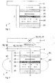
- Figs. 1 and 3 illustrate a magnetic random access memory (MRAM) cell 1 comprising a magnetic tunnel junction 2, according to an embodiment.
- the magnetic tunnel junction 2 comprises a stack including a first magnetic layer 21 having a first magnetization 210, a second magnetic layer 23 having a second magnetization 230 and a tunnel barrier layer 22 comprised between the first and second magnetic layer (21, 23).
- the first magnetization 210 can be is freely switchable such that the first magnetic layer 21 corresponds to a sense layer.
- the first magnetization 210 can be fixed in the whole range of temperature and magnetic field used during writing of the MRAM cell 1. In that latter case, the first magnetic layer 21 corresponds to a reference layer.
- the second magnetic layer 23, or storage layer, is exchange-coupled with an antiferromagnetic layer 24 such that the second magnetization 230 is pinned at a low temperature threshold and freely orientable at a high temperature threshold.
- the MRAM cell 1 can be used as a self-referenced MRAM cell.
- the storage layer 23 can comprise one or more of a CoFe, CoFeB or NiFe layer, or more generally a Co, Ni or Fe -based alloy.
- the antiferromagnetic layer 24 can comprise a manganese-based alloy, such as IrMn, PtMn or FeMn, a multilayer structure comprising a combination of manganese-based alloys, or any other suitable materials.
- the stack can further include a seed layer 25 comprising a NiFe -based alloy and being arranged such that the antiferromagnetic layer 24 is comprised between the seed layer 25 and the storage layer 23.
- the thicknesses of the seed layer 25 can be between 1 nm and 10 nm.
- the seed layer 25 comprises a NixFey alloy.
- x is equal to 81 and y is equal to 19.
- the thicknesses of the seed layer 25 can be between 1 nm and 10 nm.
- the NiFe -based alloy of the seed layer 25 further comprises nitrogen.
- Nitrogen can be incorporated in the NiFe film structure by introducing a nitrogen flow in the argon plasma during the sputtering process of the seed layer 25 Adding nitrogen in the NiFe seed layer 25 results in a reduced roughness of the seed layer 25, for example below 0.3 nm RMS.
- Other advantages of adding nitrogen to the seed layer 25 include reducing the saturation magnetization of the seed layer 25 , for example from 800 emu/cm 3 down to 0 emu/cm 3 for nonmagnetic layer, and increasing the electrical resistivity of the seed layer 25, for example from 23.5 ⁇ ohm.cm up to about 0.5 mohm.cm.
- the increased electrical resistivity of the seed layer 25 improves heating of the magnetic tunnel junction 2 during a write operation (see below).
- the increased electrical resistivity has a positive impact on the local heating of the antiferromagnetic layer 24.
- the seed layer 25 comprising the NiFeN composition has reduced Néel coupling compared to the seed layer 25 comprising NiFe.
- the reduction in Néel coupling results from the reduced roughness of the NiFeN seed layer 25.
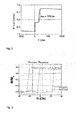
- the seed layer 25 comprises a NiFe alloy exhibiting a Néel coupling H Néel , NiFe of about -15 Oe with the magnetic tunnel junction 2 wherein the seed layer 25 comprises a NiFeN alloy exhibiting a Néel coupling H Néel , NiFeN of about 5 Oe.
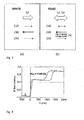
- Fig. 4 reports a hysteresis loop measured experimentally for the magnetic tunnel junction 2 wherein the seed layer comprises a NiFe alloy, the antiferromagnetic layer 24 comprises an IrMn alloy and the storage layer 23 comprises a CoFe alloy.
- Fig. 5 report another hysteresis loop measured experimentally for the same magnetic tunnel junction 2 as the one of Fig. 4 but wherein the storage layer 23 comprises a NiFe alloy, Comparison of Figs. 4 and 5 shows that the exchange bias field between antiferromagnetic layer 24 and the storage layer 23 measured in Fig. 4 (1145 Oe) is almost one order of magnitude larger than the exchange bias field measured in Fig. 5 (175 Oe).
- the most important parameter describing the exchange bias interaction is the exchange coupling constant, J ex , which is summarized in Table 1 for different combinations of seed layer 25 and ferromagnetic storage layer 23 in the presence of a IrMn antiferromagnetic layer 24.
- the storage layer 23 comprises a storage interface layer 26 including a CoFe -based alloy.
- the thickness of the storage interface layer 26 is between 0.1 nm and 10 nm, but preferentially between 0.5 nm and 2 nm.
- the storage interface layer 26 including a CoFe -based alloy allows for increasing the exchange bias field between antiferromagnetic layer 24 and the storage layer 23 even in the case the storage layer comprise the NiFe alloy.
- the CoFe interface storage layer 26, located at the interface between the storage layer 23 and the antiferromagnetic layer 24, allows for increasing the exchange magnetic bias field H ex .
- Table 1 summarises values corresponding to the exchange bias interaction J ex for different configurations the stack.
- examples 1, 2 and 3 compare configurations of the stack comprising an IrMn antiferromagnetic layer 24 and a NiFe storage layer 23 (example 3), or CoFe storage layer 23 or storage interface layer 26 (examples 1 and 2)
- the stack configuration of example 1 does not include the seed layer 25.
- Examples 4 to 6 compare configurations of the stack comprising a PtMn antiferromagnetic layer 24, the NiFe seed layer 25 and a NiFe storage layer 23 (examples 4 and 6) or CoFe storage layer 23 or storage interface layer 26 (example 5).
- Table 1 also reports the value of the saturation magnetization of the storage layer M 5 in emu/cm 3 , and the thickness in nm of the storage layer 23 for each configuration of the magnetic tunnel junction 2.
- the highest exchange bias interaction J ex (highest exchange coupling between the antiferromagnetic layer 24 and the storage layer 23) is obtained for the NiFe/IrMn/CoFe stack configuration.
- a magnetic memory device (not represented) can comprise a plurality of the MRAM cell 1 arranged in rows and columns.
- the magnetic memory device can further comprise one or a plurality of the current line 3 that connect the MRAM cells 1 along a row (or column), and possibly one or a plurality of the field line 4 coupled to the MRAM cells 1 along a column (or row).
- a thermally assisted switching (TAS) write operation comprises:
- Heating the magnetic tunnel junction 2 can comprise passing a heating current 31 in the magnetic tunnel junction 2 via a current line 3 electrically connected to an end of the magnetic tunnel junction 2 (See Fig. 2 ).
- Switching the storage magnetization 230 is performed by applying the external write magnetic field 42.
- the write magnetic field 42 can be applied by passing a write current 41 in a field line 4 in communication with the magnetic tunnel junction 2.
- the field line is shown on top of the current line 3.
- the write current 41 can be passed in the current line 3 such that the field line 4 can be avoided.
- the magnetic field 42 is applied with a magnitude such as to saturate a seed magnetization 250 of the seed layer 25 in a direction according to the direction of the write magnetic field 42 (shown oriented toward the right hand side of the page in Fig. 2 ).
- the saturated seed magnetization 250 induces in turn a local seed magnetic stray field 60 coupling the storage magnetization 230 in a closed magnetic flux configuration (see Fig. 2 ).
- the magnetic field 42 also saturates the sense magnetization 210 of the sense layer 21 such as to induce a local sense magnetic stray field 61 also coupling the sense magnetization 210 with the storage magnetization 230 (see Fig. 2 ).
- the storage magnetization 230 is oriented in accordance with a net magnetic stray field that is the sum of the seed magnetic stray field 60 and sense magnetic stray field 61.
- the seed magnetic stray field 60 increases the net magnetic stray field used for switching of the storage magnetization 230 in comparison to when only the sense magnetic stray field 61 is used.
- Figs. 2 and 3a illustrate the parallel orientations of the sense and seed magnetizations 210, 250 during the write operation.
- the storage layer 23 is thus more effectively switched with the saturated seed magnetization 250 than when switched directly with the write magnetic field 42 generated by the field line 4.
- a self-referenced read operation of the MRAM cell 1 comprises:
- Figs. 2 and 3b illustrate the relative orientations of the sense and seed magnetizations 210, 250 during the read operation.
- the storage magnetization 230 is oriented antiparallel to the seed magnetization 250 such that the seed magnetic stray field 60 is opposed to a storage magnetic stray field 62 generated by the storage magnetization 230.
- the net magnetic stray field coupling the sense layer 21, corresponding to the sum of the seed magnetic stray field 60 and the storage magnetic stray field 62 is substantially null.
- the first and second read magnetic fields 52, 54 required for orienting the sense magnetization 210 can thus be reduced.
- the first read magnetic field 52 can be applied by passing a first read field current 51 having a first polarity in the field line 4 (or in the current line 3).
- the first direction of the sense magnetization 210 is then compared with the storage magnetization 230 by passing a sense current 32 in the magnetic tunnel junction 2 via the current line 3.
- the voltage measured across the magnetic tunnel junction 2 yields a corresponding first resistance value R 1 of the magnetic tunnel junction 2.
- the second read magnetic field 54 can be applied by passing a second read field current 53 having a second polarity in the field line 4 (or in the current line 3).
- the second direction of the sense magnetization 210 is then compared with the storage magnetization 230 by passing the sense current 32 in the magnetic tunnel junction 2. Measuring a voltage across the magnetic tunnel junction 2 when the sense current 32 is passed through the magnetic tunnel junction 2 yields a corresponding second resistance value R 2 of the magnetic tunnel junction 2.
- the write operation comprises only the step of applying the first read magnetic field 52 and of determining a first resistance value R 1 .
- the first resistance value R 1 can be compared to a reference resistance typically halfway between R min and R max .
Landscapes
- Engineering & Computer Science (AREA)
- Computer Hardware Design (AREA)
- Hall/Mr Elements (AREA)
- Mram Or Spin Memory Techniques (AREA)
Abstract
The present disclosure concerns a MRAM cell (1) comprising a magnetic tunnel junction (2) comprising: a sense layer (21) having a sense magnetization (210) that is freely switchable; a storage layer (23) having a storage magnetization (230); a tunnel barrier layer (22) comprised between the sense and the storage layers (21, 23); and an antiferromagnetic layer (24) pinning the storage layer (23) at a low temperature threshold and freeing it at a high temperature threshold; wherein the tunnel magnetic junction (2) further includes a seed layer (25) comprising a NiFe -based alloy and being arranged such that the antiferromagnetic layer (24) is comprised between the seed layer (25) and the storage layer (23). The present disclosure further concerns a magnetic memory device comprising a plurality of the MRAM cell (1) and a method for writing and a self-referenced method for reading the MRAM cell (1).
Description
- The present disclosure concerns a magnetic random access memory (MRAM) cell having enhanced exchange bias field between an antiferromagnetic layer and a storage layer of the MRAM cell. The present disclosure also concerns a method for writing and reading a thermally assisted MRAM cell.
- Spintronic devices such as MRAM cells and devices based on MRAM cells, spin transfer torque oscillators or magnetic logic units, usually comprise a magnetic tunnel junction including a reference or sense layer, a tunnel barrier layer and a storage layer exchange-coupled or not with an antiferromagnetic layer. The antiferromagnetic layer is arranged to pin a magnetization of the ferromagnetic layer at a low temperature threshold and frees it a high temperature threshold via a so-called exchange bias, appearing when the antiferromagnetic layer is in contact with the ferromagnetic layer. The exchange bias is thus of great importance in the functioning of spintronic devices.
- The exchange bias phenomenon is characterized by a shifted magnetization hysteresis loop measured for pinned ferromagnetic layer, as a function of an applied magnetic field. In general, the exchange bias is impacted by the crystallographic properties induced by seed layers. Moreover, a large roughness of the seed layers on which the antiferromagnetic layer is grown can play a negative role both on magnetic switching properties of the ferromagnetic layer and on the reliability of the tunnel barrier.
- The present disclosure concerns a MRAM cell comprising a magnetic tunnel junction having a stack comprising; a sense layer having a sense magnetization; a storage layer having a storage magnetization; a tunnel barrier layer comprised between the sense and the storage layers; and an antiferromagnetic layer pinning the storage layer at a low temperature threshold and freeing it at a high temperature threshold; wherein the tunnel magnetic junction further includes a seed layer comprising a NiFe -based alloy and being arranged such that the antiferromagnetic layer is comprised between the seed layer and the storage layer.
- The present disclosure further concerns a method for writing the MRAM cell comprising:
- heating the magnetic tunnel junction at the high temperature threshold;
- once the magnetic tunnel junction has reached the high temperature threshold, switching the storage magnetization in the written state; and
- cooling the magnetic tunnel junction to the low temperature threshold such as to freeze the storage magnetizations in the written state.
- The present also pertains to a method for reading the MRAM cell wherein the sense magnetization is freely switchable (i.e., the MRAM cell having a self-referenced configuration), the method comprising:
- applying a first read magnetic field adapted for aligning the sense magnetization in a first direction;
- determining a first resistance value of the magnetic tunnel junction;
- applying a second read magnetic field adapted for aligning the sense magnetization in a second direction opposed to the first direction;
- determining a second resistance value of the magnetic tunnel junction; and
- comparing the first and second resistance values such as to determine a tunnel magnetoresistance or magnetoresistance, wherein the magnetoresistance corresponds to the ratio of the first second resistance on the second resistance.
- The MRAM cell comprising the seed layer has a high exchange bias coupling field between the antiferromagnetic layer and the storage layer, the large exchange bias coupling field being favoured by the presence of NiFe-based seed layer. An enhanced exchange bias field is advantageous for improved data retention and prevents accidental switching of the cell in presence of large external parasitic fields. Advantageously, the NiFe seed layer can have a reduced roughness by incorporating nitrogen in the film during the growth of the seed layer.
- Moreover, if the selected seed layers are magnetized, they can be advantageously used for reducing the reading and the writing fields. In particular, for the MRAM cell having the self-reference configuration, the seed layer can have a magnetization that can be advantageously used for the dipolar writing of the magnetization of the storage layer. The self-referenced MRAM cell can further be advantageously read by using a reduced magnetic field due to a stray field from the seed layer cancelling or reducing astray field coming from the storage layer.
- The invention will be better understood with the aid of the description of an embodiment given by way of example and illustrated by the figures, in which:
-
Fig. 1 illustrates a magnetic tunnel junction comprising a storage layer, a sense layer and a seed layer, according to an embodiment; -
Fig. 2 represents a MRAM cell comprising the magnetic tunnel junction ofFig. 1 , according to an embodiment; -
Fig. 3 illustrates the orientations of the sense, storage and seed magnetizations during a write operation (a) and during a read operation (b); -
Fig. 4 shows an hysteresis loop for the magnetic tunnel junction ofFig. 1 wherein the storage layer comprises a CoFe alloy, according to an embodiment; -
Fig. 5 shows an hysteresis loop for the magnetic tunnel junction ofFig. 1 wherein the storage layer comprises a NiFe alloy, according to an embodiment; -
Fig. 6 compares a hysteresis loop for the magnetic tunnel junction wherein the seed layer comprises a NiFe alloy to the magnetic tunnel junction wherein the seed layer comprises a NiFeN alloy. -
Figs. 1 and3 illustrate a magnetic random access memory (MRAM)cell 1 comprising amagnetic tunnel junction 2, according to an embodiment. Themagnetic tunnel junction 2 comprises a stack including a firstmagnetic layer 21 having afirst magnetization 210, a secondmagnetic layer 23 having asecond magnetization 230 and atunnel barrier layer 22 comprised between the first and second magnetic layer (21, 23). Thefirst magnetization 210 can be is freely switchable such that the firstmagnetic layer 21 corresponds to a sense layer. Alternatively, thefirst magnetization 210 can be fixed in the whole range of temperature and magnetic field used during writing of theMRAM cell 1. In that latter case, the firstmagnetic layer 21 corresponds to a reference layer. The secondmagnetic layer 23, or storage layer, is exchange-coupled with anantiferromagnetic layer 24 such that thesecond magnetization 230 is pinned at a low temperature threshold and freely orientable at a high temperature threshold. In this configuration, theMRAM cell 1 can be used as a self-referenced MRAM cell. Thestorage layer 23 can comprise one or more of a CoFe, CoFeB or NiFe layer, or more generally a Co, Ni or Fe -based alloy. Theantiferromagnetic layer 24 can comprise a manganese-based alloy, such as IrMn, PtMn or FeMn, a multilayer structure comprising a combination of manganese-based alloys, or any other suitable materials. The stack can further include aseed layer 25 comprising a NiFe -based alloy and being arranged such that theantiferromagnetic layer 24 is comprised between theseed layer 25 and thestorage layer 23. The thicknesses of theseed layer 25 can be between 1 nm and 10 nm. - In an embodiment, the
seed layer 25 comprises a NixFey alloy. Preferably, x is equal to 81 and y is equal to 19. The thicknesses of theseed layer 25 can be between 1 nm and 10 nm. - In another embodiment, the NiFe -based alloy of the
seed layer 25 further comprises nitrogen. Nitrogen can be incorporated in the NiFe film structure by introducing a nitrogen flow in the argon plasma during the sputtering process of theseed layer 25 Adding nitrogen in theNiFe seed layer 25 results in a reduced roughness of theseed layer 25, for example below 0.3 nm RMS. Other advantages of adding nitrogen to theseed layer 25 include reducing the saturation magnetization of theseed layer 25 , for example from 800 emu/cm3 down to 0 emu/cm3 for nonmagnetic layer, and increasing the electrical resistivity of theseed layer 25, for example from 23.5 µohm.cm up to about 0.5 mohm.cm. The increased electrical resistivity of theseed layer 25 improves heating of themagnetic tunnel junction 2 during a write operation (see below). The increased electrical resistivity has a positive impact on the local heating of theantiferromagnetic layer 24. Theseed layer 25 comprising the NiFeN composition has reduced Néel coupling compared to theseed layer 25 comprising NiFe. The reduction in Néel coupling results from the reduced roughness of theNiFeN seed layer 25.Fig. 6 compares a hysteresis loop for themagnetic tunnel junction 2 wherein theseed layer 25 comprises a NiFe alloy exhibiting a Néel coupling HNéel,NiFe of about -15 Oe with themagnetic tunnel junction 2 wherein theseed layer 25 comprises a NiFeN alloy exhibiting a Néel coupling HNéel,NiFeN of about 5 Oe. -
Fig. 4 reports a hysteresis loop measured experimentally for themagnetic tunnel junction 2 wherein the seed layer comprises a NiFe alloy, theantiferromagnetic layer 24 comprises an IrMn alloy and thestorage layer 23 comprises a CoFe alloy.Fig. 5 report another hysteresis loop measured experimentally for the samemagnetic tunnel junction 2 as the one ofFig. 4 but wherein thestorage layer 23 comprises a NiFe alloy, Comparison ofFigs. 4 and5 shows that the exchange bias field betweenantiferromagnetic layer 24 and thestorage layer 23 measured inFig. 4 (1145 Oe) is almost one order of magnitude larger than the exchange bias field measured inFig. 5 (175 Oe). In any case, the most important parameter describing the exchange bias interaction is the exchange coupling constant, Jex, which is summarized in Table 1 for different combinations ofseed layer 25 andferromagnetic storage layer 23 in the presence of a IrMnantiferromagnetic layer 24. - In yet another embodiment, the
storage layer 23 comprises astorage interface layer 26 including a CoFe -based alloy. The thickness of thestorage interface layer 26 is between 0.1 nm and 10 nm, but preferentially between 0.5 nm and 2 nm. Thestorage interface layer 26 including a CoFe -based alloy allows for increasing the exchange bias field betweenantiferromagnetic layer 24 and thestorage layer 23 even in the case the storage layer comprise the NiFe alloy. The CoFeinterface storage layer 26, located at the interface between thestorage layer 23 and theantiferromagnetic layer 24, allows for increasing the exchange magnetic bias field Hex. - Table 1 summarises values corresponding to the exchange bias interaction Jex for different configurations the stack. In particular, examples 1, 2 and 3 compare configurations of the stack comprising an IrMn
antiferromagnetic layer 24 and a NiFe storage layer 23 (example 3), orCoFe storage layer 23 or storage interface layer 26 (examples 1 and 2) In contrast to examples 2 and 3, the stack configuration of example 1 does not include theseed layer 25. Examples 4 to 6 compare configurations of the stack comprising a PtMnantiferromagnetic layer 24, theNiFe seed layer 25 and a NiFe storage layer 23 (examples 4 and 6) orCoFe storage layer 23 or storage interface layer 26 (example 5). Table 1 also reports the value of the saturation magnetization of the storage layer M5 in emu/cm3, and the thickness in nm of thestorage layer 23 for each configuration of themagnetic tunnel junction 2. The highest exchange bias interaction Jex (highest exchange coupling between theantiferromagnetic layer 24 and the storage layer 23) is obtained for the NiFe/IrMn/CoFe stack configuration. - A magnetic memory device (not represented) can comprise a plurality of the
MRAM cell 1 arranged in rows and columns. The magnetic memory device can further comprise one or a plurality of thecurrent line 3 that connect theMRAM cells 1 along a row (or column), and possibly one or a plurality of thefield line 4 coupled to theMRAM cells 1 along a column (or row).Table 1 Configuration of the stack Saturation magnetization of storage layer, M5 (emu/cm3) Thickness of storage layer (nm) Exchange coupling constant, Jex (erg/cm2) 1 IrMn-/CoFe 1550 5 0.23 2 NiFe seed ArMn/CoFe 1550 1 0.589 3 NiFe seed /irMn/NiFe 800 2 0.032 4 NiFe seed /PtMn/NiFe 800 5 0.196 5 NiFe seed /PtMn/CoFeB 1150 5 0.43 6 NiFe seed /PtMn/NiFe 800 3 0.45 - According to an embodiment, a thermally assisted switching (TAS) write operation comprises:
- heating the
magnetic tunnel junction 2 to a high temperature threshold; - once the
magnetic tunnel junction 2 has reached the high temperature threshold, switching thestorage magnetizations 230 in the written state (write data); and - cooling the
magnetic tunnel junction 2 to the low temperature threshold such as to freeze thestorage magnetizations 230 in the written state. - Heating the
magnetic tunnel junction 2 can comprise passing a heating current 31 in themagnetic tunnel junction 2 via acurrent line 3 electrically connected to an end of the magnetic tunnel junction 2 (SeeFig. 2 ). - Switching the
storage magnetization 230 is performed by applying the external writemagnetic field 42. The writemagnetic field 42 can be applied by passing a write current 41 in afield line 4 in communication with themagnetic tunnel junction 2. In the example ofFig. 2 , the field line is shown on top of thecurrent line 3. Alternatively, the write current 41 can be passed in thecurrent line 3 such that thefield line 4 can be avoided. - In an embodiment, the
magnetic field 42 is applied with a magnitude such as to saturate aseed magnetization 250 of theseed layer 25 in a direction according to the direction of the write magnetic field 42 (shown oriented toward the right hand side of the page inFig. 2 ). The saturatedseed magnetization 250 induces in turn a local seed magneticstray field 60 coupling thestorage magnetization 230 in a closed magnetic flux configuration (seeFig. 2 ). During the write operation, themagnetic field 42 also saturates thesense magnetization 210 of thesense layer 21 such as to induce a local sense magneticstray field 61 also coupling thesense magnetization 210 with the storage magnetization 230 (seeFig. 2 ). Since both seed and sense magneticstray fields storage magnetization 230 is oriented in accordance with a net magnetic stray field that is the sum of the seed magneticstray field 60 and sense magneticstray field 61. Thus, the seed magneticstray field 60 increases the net magnetic stray field used for switching of thestorage magnetization 230 in comparison to when only the sense magneticstray field 61 is used.Figs. 2 and3a illustrate the parallel orientations of the sense andseed magnetizations - The distance between the
storage layer 23 and theseed layer 25 being small, typically in the nanometer range, thestorage layer 23 is thus more effectively switched with the saturatedseed magnetization 250 than when switched directly with the writemagnetic field 42 generated by thefield line 4. - According to an embodiment, a self-referenced read operation of the
MRAM cell 1 comprises: - applying a first read magnetic field 52 adapted for aligning the
sense magnetization 210 in a first direction, in accordance with the first orientation of the first read magnetic field 52; - determining a first resistance value R1 of the
magnetic tunnel junction 2; - applying a second read magnetic field 54 adapted for aligning the
sense magnetization 210 in a second direction opposed to the first direction, in accordance with the second orientation of the second read magnetic field 54; - determining a second resistance value R2 of the
magnetic tunnel junction 2; and - comparing the first and second resistance values R1, R2 such as to determine a tunnel magnetoresistance or magnetoresistance ∧R = R1/R2.
-
Figs. 2 and3b illustrate the relative orientations of the sense andseed magnetizations storage magnetization 230 is oriented antiparallel to theseed magnetization 250 such that the seed magneticstray field 60 is opposed to a storage magneticstray field 62 generated by thestorage magnetization 230. In this arrangement, the net magnetic stray field coupling thesense layer 21, corresponding to the sum of the seed magneticstray field 60 and the storage magneticstray field 62, is substantially null. The first and second read magnetic fields 52, 54 required for orienting thesense magnetization 210 can thus be reduced. - The first read magnetic field 52 can be applied by passing a first read field current 51 having a first polarity in the field line 4 (or in the current line 3). The first direction of the
sense magnetization 210 is then compared with thestorage magnetization 230 by passing a sense current 32 in themagnetic tunnel junction 2 via thecurrent line 3. The voltage measured across themagnetic tunnel junction 2 yields a corresponding first resistance value R1 of themagnetic tunnel junction 2. In the case thesense magnetization 210 is aligned substantially parallel to thestorage magnetization 230 the first resistance value R1 is small (R1 = Rmin). On the other hand, when thesense magnetization 210 is aligned substantially antiparallel to thestorage magnetization 230 the measured first resistance value is high (R1 = Rmax). - The second read magnetic field 54 can be applied by passing a second read field current 53 having a second polarity in the field line 4 (or in the current line 3). The second direction of the
sense magnetization 210 is then compared with thestorage magnetization 230 by passing the sense current 32 in themagnetic tunnel junction 2. Measuring a voltage across themagnetic tunnel junction 2 when the sense current 32 is passed through themagnetic tunnel junction 2 yields a corresponding second resistance value R2 of themagnetic tunnel junction 2. - Alternatively, the write operation comprises only the step of applying the first read magnetic field 52 and of determining a first resistance value R1. The first resistance value R1 can be compared to a reference resistance typically halfway between Rmin and Rmax.
Reference Numbers and symbols 1 MRAM cell 2 magnetic tunnel junction 21 first magnetic layer, sense layer 210 sense magnetization 22 tunnel barrier layer 23 second magnetic layer, storage layer 230 storage magnetization 24 antiferromagnetic layer 25 seed layer 250 seed magnetization 26 storage interface layer 31 heating current 32 sense current 51 first read field current 52 first read magnetic field 53 second read field current 54 second read magnetic field 60 seed magnetic stray field 61 sense magnetic stray field 62 storage magnetic stray field Jex exchange bias interaction Hex exchange magnetic bias field HNéel,NiFe Néel coupling HNéel,NiFeN Néel coupling M5 magnetization ∧R tunnel magnetoresistance R1 first resistance value R2 second resistance value
Claims (14)
- MRAM cell (1) comprising a magnetic tunnel junction (2) comprising a stack including:a sense layer (21) having a sense magnetization (210) that is freely alignable;a storage layer (23) having a storage magnetization (230);a tunnel barrier layer (22) comprised between the sense and the storage layers (21, 23); andan antiferromagnetic layer (24) pinning the storage layer (23) at a low temperature threshold and freeing it at a high temperature threshold; characterized in thatthe tunnel magnetic junction (2) further includes a seed layer (25) comprising a NiFe -based alloy and being arranged such that the antiferromagnetic layer (24) is comprised between the seed layer (25) and the storage layer (23).
- The MRAM cell (1) according to claim 1, wherein
the seed layer (25) comprises a NixFey alloy. - The MRAM cell (1) according to claim 2, wherein
the seed layer (25) comprises a Ni81Fe19 alloy. - The MRAM cell (1) according to any of the claims 1 to 3,
wherein
the thicknesses of the seed layer (25) varies between 1 nm and 10 nm. - The MRAM cell (1) according to any of the claims 1 to 4,
wherein
the seed layer (25) further comprises nitrogen. - The MRAM cell (1) according to any of the claims 1 to 5,
wherein
the storage layer (23) comprises a Co, Ni or Fe -based alloy or one or more of a CoFe, CoFeB or NiFe layer. - The MRAM cell (1) according to any of the claims 1 to 6,
wherein
the magnetic tunnel junction (2) further comprises a storage interface layer (26) comprising a CoFe alloy at the interface between the storage layer (23) and the antiferromagnetic layer (24). - The MRAM cell (1) according to claim 7, wherein
the storage interface layer (26) has a thickness between 0.1 nm and 10 nm, and preferably between 0.5 nm and 2 nm. - A magnetic memory device comprising a plurality of the MRAM cell (1) characterized by any one of claims 1 to 8.
- A method for writing the MRAM cell (1) characterized by any one of claims 1 to 8, comprising:heating the magnetic tunnel junction (2) at the high temperature threshold;once the magnetic tunnel junction (2) has reached the high temperature threshold, switching the storage magnetization (230) in the written state; andcooling the magnetic tunnel junction (2) to the low temperature threshold such as to freeze the storage magnetizations (230) in the written state.
- The method according to claim 10, wherein
switching the storage magnetization (230) comprises applying a write magnetic field (42) such as to saturate a seed magnetization (250) of the seed layer (25);
a magnetic stray field (60) induced by the saturated seed magnetization (250) switching the storage magnetization (230). - The method according to claim 11, wherein
the magnetic field (42) further saturates the sense magnetization (210) such as to induce a sense magnetic stray field (61) oriented in the same direction as the seed magnetic stray field (60) such that the storage magnetization (230) is oriented in accordance with a net magnetic stray field being the sum of the seed magnetic stray field (60) and sense magnetic stray field (61). - A method for reading the MRAM cell (1) characterized by any one of claims 1 to 8, wherein the sense magnetization (210) is freely switchable, the method comprising:applying a first read magnetic field (52) adapted for aligning the sense magnetization (210) in a first direction;determining a first resistance value (R1) of the magnetic tunnel junction (2);applying a second read magnetic field (54) adapted for aligning the sense magnetization (210) in a second direction opposed to the first direction;determining a second resistance value (R2) of the magnetic tunnel junction (2); andcomparing the first and second resistance values (R1, R2) such as to determine a tunnel magnetoresistance or magnetoresistance (ΔR= R1/R2).
- The method according to claim 13, wherein
applying the first and second read magnetic field (52, 54) further comprises orienting the seed magnetization (250) antiparallel to the storage magnetization (230), such that the net magnetic stray field coupling the sense layer (21), corresponding to the sum of the seed magnetic stray field (60) and a storage magnetic stray field (62) generated by the storage magnetization (230), is substantially null.
Priority Applications (1)
| Application Number | Priority Date | Filing Date | Title |
|---|---|---|---|
| EP12290374.3A EP2725579A1 (en) | 2012-10-29 | 2012-10-29 | TA-MRAM cell with seed layer having improved data retention, reduced writing and reading fields |
Applications Claiming Priority (1)
| Application Number | Priority Date | Filing Date | Title |
|---|---|---|---|
| EP12290374.3A EP2725579A1 (en) | 2012-10-29 | 2012-10-29 | TA-MRAM cell with seed layer having improved data retention, reduced writing and reading fields |
Publications (1)
| Publication Number | Publication Date |
|---|---|
| EP2725579A1 true EP2725579A1 (en) | 2014-04-30 |
Family
ID=47779804
Family Applications (1)
| Application Number | Title | Priority Date | Filing Date |
|---|---|---|---|
| EP12290374.3A Withdrawn EP2725579A1 (en) | 2012-10-29 | 2012-10-29 | TA-MRAM cell with seed layer having improved data retention, reduced writing and reading fields |
Country Status (1)
| Country | Link |
|---|---|
| EP (1) | EP2725579A1 (en) |
Citations (3)
| Publication number | Priority date | Publication date | Assignee | Title |
|---|---|---|---|---|
| JPH10188229A (en) * | 1996-12-25 | 1998-07-21 | Hitachi Ltd | Stack of antiferromagnetic layer and magnetic layer and magnetic head |
| US20080232003A1 (en) * | 2007-03-20 | 2008-09-25 | Fujitsu Limited | Magnetoresistance effect device, magnetic lamination structural body, and manufacture method for magnetic lamination structural body |
| EP2276034A2 (en) * | 2009-07-13 | 2011-01-19 | Crocus Technology S.A. | Self-referenced magnetic random access memory cell |
-
2012
- 2012-10-29 EP EP12290374.3A patent/EP2725579A1/en not_active Withdrawn
Patent Citations (3)
| Publication number | Priority date | Publication date | Assignee | Title |
|---|---|---|---|---|
| JPH10188229A (en) * | 1996-12-25 | 1998-07-21 | Hitachi Ltd | Stack of antiferromagnetic layer and magnetic layer and magnetic head |
| US20080232003A1 (en) * | 2007-03-20 | 2008-09-25 | Fujitsu Limited | Magnetoresistance effect device, magnetic lamination structural body, and manufacture method for magnetic lamination structural body |
| EP2276034A2 (en) * | 2009-07-13 | 2011-01-19 | Crocus Technology S.A. | Self-referenced magnetic random access memory cell |
Non-Patent Citations (3)
| Title |
|---|
| AN L H ET AL: "High Thermal Stable MRAM With a Synthetic Ferrimagnetic Pinned Layer", IEEE TRANSACTIONS ON MAGNETICS, IEEE SERVICE CENTER, NEW YORK, NY, US, vol. 40, no. 4, 1 July 2004 (2004-07-01), pages 2634 - 2636, XP011116926, ISSN: 0018-9464, DOI: 10.1109/TMAG.2004.825035 * |
| INOMATA K: "PRESENT AND FUTURE OF MAGNETIC RAM TECHNOLOGY", IEICE TRANSACTIONS ON ELECTRONICS, INSTITUTE OF ELECTRONICS, TOKYO, JP, vol. E84-C, no. 6, 1 June 2001 (2001-06-01), pages 740 - 746, XP001060103, ISSN: 0916-8524 * |
| WANG JIANGUO ET AL: "Low-current blocking temperature writing of double barrier magnetic random access memory cells", APPLIED PHYSICS LETTERS, AIP, AMERICAN INSTITUTE OF PHYSICS, MELVILLE, NY, US, vol. 84, no. 6, 9 February 2004 (2004-02-09), pages 945 - 947, XP012062056, ISSN: 0003-6951, DOI: 10.1063/1.1646211 * |
Similar Documents
| Publication | Publication Date | Title |
|---|---|---|
| USRE47975E1 (en) | Perpendicular magnetic tunnel junction (pMTJ) with in-plane magneto-static switching-enhancing layer | |
| US8758909B2 (en) | Scalable magnetoresistive element | |
| US11776726B2 (en) | Dipole-coupled spin-orbit torque structure | |
| US7965543B2 (en) | Method for reducing current density in a magnetoelectronic device | |
| US8331141B2 (en) | Multibit cell of magnetic random access memory with perpendicular magnetization | |
| EP1970911B1 (en) | Spin-polarised current driven magnetic memory device and memory | |
| US7973349B2 (en) | Magnetic device having multilayered free ferromagnetic layer | |
| US8670271B2 (en) | Magnetic stack having assist layers | |
| US8912614B2 (en) | Magnetic tunnel junction devices having magnetic layers formed on composite, obliquely deposited seed layers | |
| US8988934B2 (en) | Multibit cell of magnetic random access memory with perpendicular magnetization | |
| US7613036B2 (en) | Memory element utilizing magnetization switching caused by spin accumulation and spin RAM device using the memory element | |
| US20130307097A1 (en) | Magnetoresistive random access memory cell design | |
| US20110129691A1 (en) | Domain wall motion element and magnetic random access memory | |
| US8289756B2 (en) | Non volatile memory including stabilizing structures | |
| US9680088B2 (en) | Ferromagnetic tunnel junction element and method of driving ferromagnetic tunnel junction element | |
| US8344467B2 (en) | Storage element and storage device | |
| TWI482152B (en) | Memory device, memory device | |
| US20150287450A1 (en) | Thermally assisted mram cell and method for writing a plurality of bits in the mram cell | |
| US11631804B2 (en) | Magnetoresistive effect element and magnetic memory | |
| KR20130079198A (en) | Self-referenced mram cell and method for writing the cell using a spin transfer torque write operation | |
| US20160012874A1 (en) | Self-referenced mram cell that can be read with reduced power consumption | |
| US9679624B2 (en) | Magnetic random access memory (MRAM) cell with low power consumption | |
| JP2003188359A (en) | Magneto-resistive device including magnetically soft synthetic ferrimagnet reference layer | |
| JP4766835B2 (en) | Magnetic random access memory cell using magnetostatic coupling | |
| JP2005174969A5 (en) |
Legal Events
| Date | Code | Title | Description |
|---|---|---|---|
| PUAI | Public reference made under article 153(3) epc to a published international application that has entered the european phase |
Free format text: ORIGINAL CODE: 0009012 |
|
| 17P | Request for examination filed |
Effective date: 20121029 |
|
| AK | Designated contracting states |
Kind code of ref document: A1 Designated state(s): AL AT BE BG CH CY CZ DE DK EE ES FI FR GB GR HR HU IE IS IT LI LT LU LV MC MK MT NL NO PL PT RO RS SE SI SK SM TR |
|
| AX | Request for extension of the european patent |
Extension state: BA ME |
|
| STAA | Information on the status of an ep patent application or granted ep patent |
Free format text: STATUS: THE APPLICATION IS DEEMED TO BE WITHDRAWN |
|
| 18D | Application deemed to be withdrawn |
Effective date: 20141031 |