EP2725446A1 - Electronic circuit arrangement with ground and reference electric potential - Google Patents
Electronic circuit arrangement with ground and reference electric potential Download PDFInfo
- Publication number
- EP2725446A1 EP2725446A1 EP13275211.4A EP13275211A EP2725446A1 EP 2725446 A1 EP2725446 A1 EP 2725446A1 EP 13275211 A EP13275211 A EP 13275211A EP 2725446 A1 EP2725446 A1 EP 2725446A1
- Authority
- EP
- European Patent Office
- Prior art keywords
- voltage
- circuit part
- ground
- node
- supply voltage
- Prior art date
- Legal status (The legal status is an assumption and is not a legal conclusion. Google has not performed a legal analysis and makes no representation as to the accuracy of the status listed.)
- Withdrawn
Links
- 230000010355 oscillation Effects 0.000 claims description 4
- 238000002955 isolation Methods 0.000 description 6
- 238000004891 communication Methods 0.000 description 4
- 238000010586 diagram Methods 0.000 description 4
- 230000008901 benefit Effects 0.000 description 2
- 239000003990 capacitor Substances 0.000 description 2
- 238000013461 design Methods 0.000 description 1
- 238000005516 engineering process Methods 0.000 description 1
- 238000000034 method Methods 0.000 description 1
- 238000012986 modification Methods 0.000 description 1
- 230000004048 modification Effects 0.000 description 1
- 238000012545 processing Methods 0.000 description 1
- 239000004065 semiconductor Substances 0.000 description 1
- 230000000087 stabilizing effect Effects 0.000 description 1
- 239000000758 substrate Substances 0.000 description 1
Images

Classifications
-
- G—PHYSICS
- G05—CONTROLLING; REGULATING
- G05F—SYSTEMS FOR REGULATING ELECTRIC OR MAGNETIC VARIABLES
- G05F1/00—Automatic systems in which deviations of an electric quantity from one or more predetermined values are detected at the output of the system and fed back to a device within the system to restore the detected quantity to its predetermined value or values, i.e. retroactive systems
- G05F1/10—Regulating voltage or current
- G05F1/46—Regulating voltage or current wherein the variable actually regulated by the final control device is DC
- G05F1/56—Regulating voltage or current wherein the variable actually regulated by the final control device is DC using semiconductor devices in series with the load as final control devices
-
- G—PHYSICS
- G05—CONTROLLING; REGULATING
- G05F—SYSTEMS FOR REGULATING ELECTRIC OR MAGNETIC VARIABLES
- G05F5/00—Systems for regulating electric variables by detecting deviations in the electric input to the system and thereby controlling a device within the system to obtain a regulated output
Definitions
- the present invention relates to an electronic circuit arrangement which is applicable to an electronic shelf label (ESL) system and the like and having an isolated reference electric potential from the ground for ground isolation.
- ESL electronic shelf label
- an electronic shelf label (ESL) system is a system for automatically providing merchandise information and may include a plurality of tag devices (terminals indicating prices), a relay (e.g., a gateway) and a server.
- tag devices terminal indicating prices
- relay e.g., a gateway
- server e.g., a server
- the tags may establish a wireless network to perform wireless communication with the relay (GW, gateway), and the relay may perform wired or wireless communication with the server.
- the tag devices of such an electronic shelf label system may include a plurality of circuit chips and communication chips.
- a guard ring or a deep N well is used for reducing power noise coming through a substrate.
- a method of using a guard ring to reduce noise between blocks is effective, provided that the guard ring is thick and a spacing distance is sufficient, providing a guard ring for each block increases the number of the guard rings used and thus a chip area may be increased.
- Patent Document 1 relates to a mike circuit and discloses separated ground, but does not disclose a circuit having a separated reference electric potential for ground isolation.
- An aspect of the present invention provides an electronic circuit arrangement having a reference electric potential isolated from a ground for ground isolation.
- an electronic circuit arrangement including: a first circuit part disposed between a supply voltage node and a ground node and using the supply voltage as an operating voltage thereof so as to provide a predetermined reference voltage; and a second circuit part disposed between the supply voltage node and the reference voltage node and using a difference voltage between the supply voltage and the reference voltage as an operating voltage thereof.
- the first circuit part may generate the reference voltage to be lower than the supply voltage and higher than the ground potential.
- the first circuit part may include a regulator generating the predetermined reference voltage so that the difference voltage corresponds to the rated voltage of the second circuit part.
- the second circuit part may use the reference voltage as a reference electric potential.
- the second circuit part may include a voltage-controlled oscillator generating a predetermined oscillation signal by using the difference voltage as an operating voltage thereof.
- FIG. 1 is a block diagram of an electronic circuit arrangement according to an embodiment of the present invention.
- the electronic circuit arrangement may include a first circuit part 100 and a second circuit part 200.
- the first circuit part 100 has the ground as its reference electric potential, while the second circuit part 200 does not have the ground but has the reference voltage Vref provided from the first circuit part 100 as its reference electric potential.
- the first circuit part 100 is disposed between the supply voltage Vdd node and the ground node so that it may provide a predetermined reference voltage Vref to the reference electric potential node of the second circuit part 200 using the supply voltage Vdd as the operating voltage.
- the second circuit part 200 is disposed between the supply voltage Vdd node and the reference voltage Vref node so that it may use the difference voltage Vdif between the supply voltage Vdd and the reference voltage Vref as the operating voltage.
- the first and second circuit parts 100 and 200 share the ground so that they are influenced by phase noise through the ground.
- the reference electric potential node of the second circuit part 200 is connected not to the ground but to the reference voltage Vref node in order to receive the reference voltage Vref provided from the first circuit part 100.
- FIG. 2 is a block diagram in which an electronic circuit arrangement according to an embodiment of the present invention is implemented.
- the first circuit part 100 may generate the reference voltage Vref lower than the supply voltage Vdd and higher than the ground potential.
- the first circuit part 100 may include a regulator that generates the predetermined reference voltage Vref such that the difference voltage Vdif corresponds to the rated voltage of the second circuit part 200.
- the regulator is operated by the supply voltage Vdd of 3.0 V, generates the reference voltage Vref of 1.2 V, and provides it to the reference electric potential node of the second circuit part 200.
- the second circuit part 200 may be configured to use the reference voltage Vref as the reference electric potential.
- the second circuit part 200 may include a voltage-controlled oscillator VCO that uses the difference voltage Vdif as the operating voltage to generate a predetermined oscillation signal.
- the voltage-controlled oscillator VCO uses 1.8 V as the operating voltage which is the difference voltage Vdif between the supply voltage Vdd of 3.0 V and the reference voltage Vref of 1.2 V from the first circuit part 100.
- the voltage-controlled oscillator VCO may use the difference voltage Vdif of 1.8 V as the operating voltage so as to generate a predetermined oscillation signal.
- the embodiment of the present invention is designed to use a certain voltage as the reference electric potential instead of the lowest voltage GND which is vulnerable to noise.
- This design enables a power source to be connected to the main power of a chip so that a power noise source can be prevented.
- the ground GND and the ground GND of other circuit blocks since there is a difference between the ground GND and the ground GND of other circuit blocks, it is resistant to noise of other circuit blocks.
- the regulator does not have any load current so that no amplifier for amplitude or gain is necessary, and no large capacitor for stabilizing is required, it is not necessary to lead the output line of the regulator out of a chip so that I/O of the chip may be efficiently utilized. Further, the range of the operating voltage of the voltage-controlled oscillator VCO may be widened by designing the circuit to be varied according to the supply voltage Vdd.
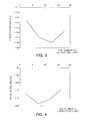
- FIGS. 3 and 4 are graphs showing phase noise characteristics.
- FIG. 3 is a graph showing phase noise in a case that the supply voltage Vdd is 2.0 V and the second circuit part 200 is a voltage-controlled oscillator
- FIG. 4 is a graph showing phase noise in a case that the supply voltage Vdd is 3.0 V and the second circuit part 200 is a voltage-controlled oscillator.
- the voltage-controlled oscillator according to the embodiment of the present invention exhibits an excellent phase noise of 100 dBc/Hz or less even with a higher operating voltage or a lower supply voltage, regardless of the number of capacitors used.
- power noise source can be blocked by way of using a reference electric potential separated from the ground for ground isolation, and thereby isolation between the ground and the reference electric potential can be obtained.
Landscapes
- Engineering & Computer Science (AREA)
- Physics & Mathematics (AREA)
- Electromagnetism (AREA)
- General Physics & Mathematics (AREA)
- Radar, Positioning & Navigation (AREA)
- Automation & Control Theory (AREA)
- Semiconductor Integrated Circuits (AREA)
Abstract
There is provided an electronic circuit arrangement with ground and reference electric potentials, the arrangement including: a first circuit part disposed between a supply voltage node and a ground node and using the supply voltage as an operating voltage thereof so as to provide a predetermined reference voltage; and a second circuit part disposed between the supply voltage node and the reference voltage node and using a difference voltage between the supply voltage and the reference voltage as an operating voltage thereof.
Description
- This application claims the benefit of Korean Patent Application No.
10-2012-0118083 filed on October 23, 2012 - The present invention relates to an electronic circuit arrangement which is applicable to an electronic shelf label (ESL) system and the like and having an isolated reference electric potential from the ground for ground isolation.
- In general, an electronic shelf label (ESL) system is a system for automatically providing merchandise information and may include a plurality of tag devices (terminals indicating prices), a relay (e.g., a gateway) and a server.
- The tags may establish a wireless network to perform wireless communication with the relay (GW, gateway), and the relay may perform wired or wireless communication with the server.
- The tag devices of such an electronic shelf label system may include a plurality of circuit chips and communication chips.
- As the technology of semiconductor processing evolves, line widths are getting smaller and most communication chips are fabricated as system on chips (SOCs). In addition, analog and digital circuits are integrated into a single chip. The biggest problem arising in the case of analog and digital circuits being integrated into a single chip is power noise.
- In particular, in a voltage-controlled oscillator generating frequencies, noise generated in a power source directly causes phase noise to be lowered. For this reason, the power source of a voltage controlled oscillator is physically separated from the power sources of other circuits.
- Often, in order to reduce clock noise in a digital circuit, a guard ring or a deep N well is used for reducing power noise coming through a substrate.
- In order to reduce noise between circuits, it is common to use separate independent power sources.
- However, the increased number of independent power sources results in an increased chip size, and isolation between blocks may not be obtained unless the ground is isolated.
- Further, although a method of using a guard ring to reduce noise between blocks is effective, provided that the guard ring is thick and a spacing distance is sufficient, providing a guard ring for each block increases the number of the guard rings used and thus a chip area may be increased.
- Patent Document 1 relates to a mike circuit and discloses separated ground, but does not disclose a circuit having a separated reference electric potential for ground isolation.
-
- (Patent Document 1) Korean Patent Laid-Open Publication No.
10-2005-0028587 - An aspect of the present invention provides an electronic circuit arrangement having a reference electric potential isolated from a ground for ground isolation.
- According to an aspect of the present invention, there is provided an electronic circuit arrangement including: a first circuit part disposed between a supply voltage node and a ground node and using the supply voltage as an operating voltage thereof so as to provide a predetermined reference voltage; and a second circuit part disposed between the supply voltage node and the reference voltage node and using a difference voltage between the supply voltage and the reference voltage as an operating voltage thereof.
- The first circuit part may generate the reference voltage to be lower than the supply voltage and higher than the ground potential.
- The first circuit part may include a regulator generating the predetermined reference voltage so that the difference voltage corresponds to the rated voltage of the second circuit part.
- The second circuit part may use the reference voltage as a reference electric potential.
- The second circuit part may include a voltage-controlled oscillator generating a predetermined oscillation signal by using the difference voltage as an operating voltage thereof.
- The above and other aspects, features and other advantages of the present invention will be more clearly understood from the following detailed description taken in conjunction with the accompanying drawings, in which:
-
FIG. 1 is a block diagram of an electronic circuit arrangement according to an embodiment of the present invention; -
FIG. 2 is a block diagram in which an electronic circuit arrangement according to an embodiment of the present invention is implemented; and -
FIGS. 3 and 4 are graphs showing phase noise characteristics. - Hereinafter, embodiments of the present invention will be described in detail with reference to the accompanying drawings. The invention may, however, be embodied in many different forms and should not be construed as being limited to the embodiments set forth herein. Rather, these embodiments are provided so that this disclosure will be thorough and complete, and will fully convey the scope of the invention to those skilled in the art. Throughout the drawings, the same or like reference numerals will be used to designate the same or like elements.
-
FIG. 1 is a block diagram of an electronic circuit arrangement according to an embodiment of the present invention. - Referring to
FIG. 1 , the electronic circuit arrangement according to the embodiment of the present invention may include afirst circuit part 100 and asecond circuit part 200. - The
first circuit part 100 has the ground as its reference electric potential, while thesecond circuit part 200 does not have the ground but has the reference voltage Vref provided from thefirst circuit part 100 as its reference electric potential. - The
first circuit part 100 is disposed between the supply voltage Vdd node and the ground node so that it may provide a predetermined reference voltage Vref to the reference electric potential node of thesecond circuit part 200 using the supply voltage Vdd as the operating voltage. - The
second circuit part 200 is disposed between the supply voltage Vdd node and the reference voltage Vref node so that it may use the difference voltage Vdif between the supply voltage Vdd and the reference voltage Vref as the operating voltage. - If the reference electric potential node of the
second circuit part 200 is connected to the ground as in the related art, the first andsecond circuit parts - In contrast, according to the embodiment of the present invention, the reference electric potential node of the
second circuit part 200 is connected not to the ground but to the reference voltage Vref node in order to receive the reference voltage Vref provided from thefirst circuit part 100. -
FIG. 2 is a block diagram in which an electronic circuit arrangement according to an embodiment of the present invention is implemented. - Referring to
FIG. 2 , thefirst circuit part 100 may generate the reference voltage Vref lower than the supply voltage Vdd and higher than the ground potential. - The
first circuit part 100 may include a regulator that generates the predetermined reference voltage Vref such that the difference voltage Vdif corresponds to the rated voltage of thesecond circuit part 200. - For example, assuming that the supply voltage Vdd is 3.0 V and the rated voltage of the
second circuit part 200 is 1.8 V, in case that thefirst circuit part 100 is a regulator, the regulator is operated by the supply voltage Vdd of 3.0 V, generates the reference voltage Vref of 1.2 V, and provides it to the reference electric potential node of thesecond circuit part 200. - The
second circuit part 200 may be configured to use the reference voltage Vref as the reference electric potential. - The
second circuit part 200 may include a voltage-controlled oscillator VCO that uses the difference voltage Vdif as the operating voltage to generate a predetermined oscillation signal. - For example, assuming that the supply voltage Vdd is 3.0 V and the rated voltage of the
second circuit part 200 is 1.8 V, in case that thesecond circuit part 200 is a voltage-controlled oscillator VCO, the voltage-controlled oscillator VCO uses 1.8 V as the operating voltage which is the difference voltage Vdif between the supply voltage Vdd of 3.0 V and the reference voltage Vref of 1.2 V from thefirst circuit part 100. - The voltage-controlled oscillator VCO may use the difference voltage Vdif of 1.8 V as the operating voltage so as to generate a predetermined oscillation signal.
- As described above, the embodiment of the present invention is designed to use a certain voltage as the reference electric potential instead of the lowest voltage GND which is vulnerable to noise. This design enables a power source to be connected to the main power of a chip so that a power noise source can be prevented. In addition, since there is a difference between the ground GND and the ground GND of other circuit blocks, it is resistant to noise of other circuit blocks.
- Moreover, since the regulator does not have any load current so that no amplifier for amplitude or gain is necessary, and no large capacitor for stabilizing is required, it is not necessary to lead the output line of the regulator out of a chip so that I/O of the chip may be efficiently utilized. Further, the range of the operating voltage of the voltage-controlled oscillator VCO may be widened by designing the circuit to be varied according to the supply voltage Vdd.
-
FIGS. 3 and 4 are graphs showing phase noise characteristics. -
FIG. 3 is a graph showing phase noise in a case that the supply voltage Vdd is 2.0 V and thesecond circuit part 200 is a voltage-controlled oscillator, andFIG. 4 is a graph showing phase noise in a case that the supply voltage Vdd is 3.0 V and thesecond circuit part 200 is a voltage-controlled oscillator. - As can be seen from
FIGS. 3 and 4 , the voltage-controlled oscillator according to the embodiment of the present invention exhibits an excellent phase noise of 100 dBc/Hz or less even with a higher operating voltage or a lower supply voltage, regardless of the number of capacitors used. - As set forth above, according to embodiments of the present invention, power noise source can be blocked by way of using a reference electric potential separated from the ground for ground isolation, and thereby isolation between the ground and the reference electric potential can be obtained.
- While the present invention has been shown and described in connection with the embodiments, it will be apparent to those skilled in the art that modifications and variations can be made without departing from the spirit and scope of the invention as defined by the appended claims.
Claims (5)
- An electronic circuit arrangement comprising:a first circuit part disposed between a supply voltage node and a ground node and using the supply voltage as an operating voltage thereof so as to provide a predetermined reference voltage; anda second circuit part disposed between the supply voltage node and the reference voltage node and using a difference voltage between the supply voltage and the reference voltage as an operating voltage thereof.
- The arrangement of claim 1, wherein the first circuit part generates the reference voltage to be lower than the supply voltage and higher than the ground potential.
- The arrangement of claim 1, wherein the first circuit part includes a regulator generating the predetermined reference voltage so that the difference voltage corresponds to the rated voltage of the second circuit part.
- The arrangement of claim 1, wherein the second circuit part uses the reference voltage as a reference electric potential.
- The arrangement of claim 1, wherein the second circuit part includes a voltage-controlled oscillator generating a predetermined oscillation signal by using the difference voltage as an operating voltage thereof.
Applications Claiming Priority (1)
| Application Number | Priority Date | Filing Date | Title |
|---|---|---|---|
| KR1020120118083A KR20140051714A (en) | 2012-10-23 | 2012-10-23 | Electronic circuit apparatus with ground and reference electric potential |
Publications (1)
| Publication Number | Publication Date |
|---|---|
| EP2725446A1 true EP2725446A1 (en) | 2014-04-30 |
Family
ID=49165682
Family Applications (1)
| Application Number | Title | Priority Date | Filing Date |
|---|---|---|---|
| EP13275211.4A Withdrawn EP2725446A1 (en) | 2012-10-23 | 2013-09-12 | Electronic circuit arrangement with ground and reference electric potential |
Country Status (2)
| Country | Link |
|---|---|
| EP (1) | EP2725446A1 (en) |
| KR (1) | KR20140051714A (en) |
Cited By (1)
| Publication number | Priority date | Publication date | Assignee | Title |
|---|---|---|---|---|
| CN119479568A (en) * | 2023-08-09 | 2025-02-18 | 格科微电子(上海)有限公司 | Power generation circuit, display drive circuit |
Citations (6)
| Publication number | Priority date | Publication date | Assignee | Title |
|---|---|---|---|---|
| US3581104A (en) * | 1970-03-05 | 1971-05-25 | Hornischfeger Corp | Voltage splitter circuit |
| JPS59188715A (en) * | 1983-04-08 | 1984-10-26 | Fujitsu Ltd | Constant-voltage circuit |
| WO2004102628A2 (en) * | 2003-05-08 | 2004-11-25 | The Trustees Of Columbia University In The City Of New York | Examiner |
| KR20050028587A (en) | 2003-09-19 | 2005-03-23 | 주식회사 팬택 | Mike circuit |
| US20070241737A1 (en) * | 2006-04-13 | 2007-10-18 | Novatek Microelectronics Corp. | Current source apparatus for reducing interference with noise |
| US20110115554A1 (en) * | 2009-11-18 | 2011-05-19 | Pelley Perry H | System having multiple voltage tiers and method therefor |
-
2012
- 2012-10-23 KR KR1020120118083A patent/KR20140051714A/en not_active Withdrawn
-
2013
- 2013-09-12 EP EP13275211.4A patent/EP2725446A1/en not_active Withdrawn
Patent Citations (6)
| Publication number | Priority date | Publication date | Assignee | Title |
|---|---|---|---|---|
| US3581104A (en) * | 1970-03-05 | 1971-05-25 | Hornischfeger Corp | Voltage splitter circuit |
| JPS59188715A (en) * | 1983-04-08 | 1984-10-26 | Fujitsu Ltd | Constant-voltage circuit |
| WO2004102628A2 (en) * | 2003-05-08 | 2004-11-25 | The Trustees Of Columbia University In The City Of New York | Examiner |
| KR20050028587A (en) | 2003-09-19 | 2005-03-23 | 주식회사 팬택 | Mike circuit |
| US20070241737A1 (en) * | 2006-04-13 | 2007-10-18 | Novatek Microelectronics Corp. | Current source apparatus for reducing interference with noise |
| US20110115554A1 (en) * | 2009-11-18 | 2011-05-19 | Pelley Perry H | System having multiple voltage tiers and method therefor |
Cited By (1)
| Publication number | Priority date | Publication date | Assignee | Title |
|---|---|---|---|---|
| CN119479568A (en) * | 2023-08-09 | 2025-02-18 | 格科微电子(上海)有限公司 | Power generation circuit, display drive circuit |
Also Published As
| Publication number | Publication date |
|---|---|
| KR20140051714A (en) | 2014-05-02 |
Similar Documents
| Publication | Publication Date | Title |
|---|---|---|
| US12013421B2 (en) | Electronic circuit and sensor system | |
| US8816768B2 (en) | Power module for envelope tracking | |
| KR101714941B1 (en) | Linear voltage regulator based on-die grid | |
| US9639133B2 (en) | Accurate power-on detector | |
| KR101818313B1 (en) | Two-stage low-dropout linear power supply systems and methods | |
| JP7059255B2 (en) | High speed driver with adaptive termination impedance | |
| JP2012190216A (en) | Constant-voltage power supply circuit | |
| US10181788B2 (en) | Rational conversion ratio converter | |
| US20160099645A1 (en) | Voltage regulator | |
| US20150022922A1 (en) | Power supply circuit for power control chips | |
| US11290059B2 (en) | Crystal oscillator interconnect architecture with noise immunity | |
| US20120161857A1 (en) | Charge pump circuit | |
| US10630297B2 (en) | Oscillator circuit and associated oscillator device | |
| KR20140051714A (en) | Electronic circuit apparatus with ground and reference electric potential | |
| Amin et al. | A wirelessly powered low‐power digital temperature sensor | |
| US9991882B2 (en) | Semiconductor apparatus | |
| JP2016092195A (en) | Power supply circuit, electronic circuit and integrated circuit | |
| CN110349928A (en) | System on chip, circuit and the method to power to the load | |
| US20120013414A1 (en) | Crystal oscillator circuit for adjusting resonant frequency of crystal oscillator | |
| US20200067462A1 (en) | High frequency amplifier | |
| JP6263435B2 (en) | Semiconductor integrated circuit | |
| US11764204B2 (en) | Electrostatic discharge and overdrive protection circuitry | |
| US20250096779A1 (en) | Filter circuitry and circuitry comprising the same | |
| JP6169804B2 (en) | Sensor device | |
| US9921592B2 (en) | Bandgap reference circuit with low output impedance stage and power-on detector |
Legal Events
| Date | Code | Title | Description |
|---|---|---|---|
| PUAI | Public reference made under article 153(3) epc to a published international application that has entered the european phase |
Free format text: ORIGINAL CODE: 0009012 |
|
| 17P | Request for examination filed |
Effective date: 20130912 |
|
| AK | Designated contracting states |
Kind code of ref document: A1 Designated state(s): AL AT BE BG CH CY CZ DE DK EE ES FI FR GB GR HR HU IE IS IT LI LT LU LV MC MK MT NL NO PL PT RO RS SE SI SK SM TR |
|
| AX | Request for extension of the european patent |
Extension state: BA ME |
|
| STAA | Information on the status of an ep patent application or granted ep patent |
Free format text: STATUS: THE APPLICATION IS DEEMED TO BE WITHDRAWN |
|
| 18D | Application deemed to be withdrawn |
Effective date: 20141031 |