EP2722925B1 - Compact twist for connecting orthogonal waveguides - Google Patents
Compact twist for connecting orthogonal waveguides Download PDFInfo
- Publication number
- EP2722925B1 EP2722925B1 EP13179001.6A EP13179001A EP2722925B1 EP 2722925 B1 EP2722925 B1 EP 2722925B1 EP 13179001 A EP13179001 A EP 13179001A EP 2722925 B1 EP2722925 B1 EP 2722925B1
- Authority
- EP
- European Patent Office
- Prior art keywords
- input
- bar
- output
- waveguide
- dipole
- Prior art date
- Legal status (The legal status is an assumption and is not a legal conclusion. Google has not performed a legal analysis and makes no representation as to the accuracy of the status listed.)
- Not-in-force
Links
- 230000005684 electric field Effects 0.000 claims description 24
- 230000005672 electromagnetic field Effects 0.000 claims description 20
- 230000001902 propagating effect Effects 0.000 claims description 8
- 238000003780 insertion Methods 0.000 claims description 7
- 230000037431 insertion Effects 0.000 claims description 7
- 239000004033 plastic Substances 0.000 description 15
- 239000002184 metal Substances 0.000 description 10
- 230000005855 radiation Effects 0.000 description 10
- 238000000034 method Methods 0.000 description 8
- 230000005670 electromagnetic radiation Effects 0.000 description 4
- 238000003754 machining Methods 0.000 description 3
- 239000011248 coating agent Substances 0.000 description 2
- 238000000576 coating method Methods 0.000 description 2
- 238000010586 diagram Methods 0.000 description 2
- 239000002991 molded plastic Substances 0.000 description 2
- 230000006978 adaptation Effects 0.000 description 1
- 239000004020 conductor Substances 0.000 description 1
- 230000008878 coupling Effects 0.000 description 1
- 238000010168 coupling process Methods 0.000 description 1
- 238000005859 coupling reaction Methods 0.000 description 1
- 239000003574 free electron Substances 0.000 description 1
- 238000004519 manufacturing process Methods 0.000 description 1
- 238000004806 packaging method and process Methods 0.000 description 1
- 230000010287 polarization Effects 0.000 description 1
- 239000000725 suspension Substances 0.000 description 1
Images




Classifications
-
- H—ELECTRICITY
- H01—ELECTRIC ELEMENTS
- H01P—WAVEGUIDES; RESONATORS, LINES, OR OTHER DEVICES OF THE WAVEGUIDE TYPE
- H01P1/00—Auxiliary devices
- H01P1/02—Bends; Corners; Twists
- H01P1/022—Bends; Corners; Twists in waveguides of polygonal cross-section
-
- H—ELECTRICITY
- H01—ELECTRIC ELEMENTS
- H01P—WAVEGUIDES; RESONATORS, LINES, OR OTHER DEVICES OF THE WAVEGUIDE TYPE
- H01P1/00—Auxiliary devices
- H01P1/06—Movable joints, e.g. rotating joints
- H01P1/062—Movable joints, e.g. rotating joints the relative movement being a rotation
- H01P1/063—Movable joints, e.g. rotating joints the relative movement being a rotation with a limited angle of rotation
- H01P1/065—Movable joints, e.g. rotating joints the relative movement being a rotation with a limited angle of rotation the axis of rotation being parallel to the transmission path, e.g. stepped twist
-
- H—ELECTRICITY
- H01—ELECTRIC ELEMENTS
- H01P—WAVEGUIDES; RESONATORS, LINES, OR OTHER DEVICES OF THE WAVEGUIDE TYPE
- H01P1/00—Auxiliary devices
- H01P1/165—Auxiliary devices for rotating the plane of polarisation
-
- H—ELECTRICITY
- H01—ELECTRIC ELEMENTS
- H01P—WAVEGUIDES; RESONATORS, LINES, OR OTHER DEVICES OF THE WAVEGUIDE TYPE
- H01P1/00—Auxiliary devices
- H01P1/165—Auxiliary devices for rotating the plane of polarisation
- H01P1/17—Auxiliary devices for rotating the plane of polarisation for producing a continuously rotating polarisation, e.g. circular polarisation
- H01P1/173—Auxiliary devices for rotating the plane of polarisation for producing a continuously rotating polarisation, e.g. circular polarisation using a conductive element
-
- H—ELECTRICITY
- H01—ELECTRIC ELEMENTS
- H01P—WAVEGUIDES; RESONATORS, LINES, OR OTHER DEVICES OF THE WAVEGUIDE TYPE
- H01P5/00—Coupling devices of the waveguide type
- H01P5/08—Coupling devices of the waveguide type for linking dissimilar lines or devices
- H01P5/082—Transitions between hollow waveguides of different shape, e.g. between a rectangular and a circular waveguide
-
- Y—GENERAL TAGGING OF NEW TECHNOLOGICAL DEVELOPMENTS; GENERAL TAGGING OF CROSS-SECTIONAL TECHNOLOGIES SPANNING OVER SEVERAL SECTIONS OF THE IPC; TECHNICAL SUBJECTS COVERED BY FORMER USPC CROSS-REFERENCE ART COLLECTIONS [XRACs] AND DIGESTS
- Y10—TECHNICAL SUBJECTS COVERED BY FORMER USPC
- Y10T—TECHNICAL SUBJECTS COVERED BY FORMER US CLASSIFICATION
- Y10T29/00—Metal working
- Y10T29/49—Method of mechanical manufacture
- Y10T29/49002—Electrical device making
- Y10T29/49016—Antenna or wave energy "plumbing" making
Definitions
- the axial orientation of the waveguide may be required to change from an H-plane orientation to an E-plane orientation or the other way around.
- an E-plane is the plane containing the electric field vector in the direction of maximum radiation.
- An H-plane is the plane containing the magnetic field vector in the direction of maximum radiation.
- the magnetizing field or H-plane is orthogonal to the E-plane.
- the electric field or E-plane determines the polarization and orientation of the radio wave.
- the E-plane usually coincides with the vertical/elevation plane and the H-plane coincides with the horizontal/azimuth plane.
- the E-plane usually coincides with the horizontal/azimuth plane and the H-plane coincides with the vertical/elevation plane.
- US 2004/0246062 discloses a waveguide unit including a vertically polarised waveguide, a horizontally polarised waveguide, and a waveguide type-polarised wave converter interposed between said waveguides.
- the waveguide type-polarised wave converter has a slit, the shape of which being a combination of two quadrate parts and a connecting part for connecting the two quadrate parts.
- Some systems require the rotation of the electro-magnetic fields from an H-plane orientation to an E-plane orientation.
- a twist or rotation of the E-field is done by a waveguide that physically forces the rotation of the orientation of the E-field (and H-field) by 90 degrees as the electro-magnetic (EM) radiation propagates along the length of the waveguide.
- EM electro-magnetic
- Some systems such as a power dividing network for an antenna array, require the rotation from an H-plane orientation to an E-plane orientation to occur over a very short distance so the twist (rotation of the E-field) occurs in the shortest length possible.
- Some shorter length twists are currently available.
- a quarter wavelength section orientated at 45 degrees is placed between the orthogonal waveguides.
- a resonant iris orientated at 45 degrees is placed between the orthogonal waveguides.
- a resonant iris can take various forms but is typically an approximately half wavelength slot at the desired frequency, separating the input and output sections of waveguide. Both the quarter wavelength section and the resonant iris have a narrow bandwidth and are sensitive to bandwidth.
- a resonant iris is also sensitive to machining tolerances due to narrow gaps in the iris.
- the present application relates to a compact interfacing device for rotating electro-magnetic fields between an input waveguide and an output waveguide.
- the interfacing device includes a support bar extending between and connected to opposing sides of a frame.
- the support bar has a support-bar length and a support-bar thickness.
- the frame encircles an interior space divided by the support bar.
- the frame has a frame thickness.
- the interfacing device also includes a dipole bar orientated orthogonal to the support bar.
- the dipole bar has a dipole-bar thickness and a dipole-bar length that is less than the support-bar length.
- the input waveguide interfaces an input-side of the frame and is arranged so that an extent of an input width of the input waveguide is orientated at first angle with respect to an extent of the dipole-bar length
- the output waveguide interfaces an output-side of the frame and is arranged so that an extent of an output width of the output waveguide is orientated at a second angle with respect to the extent of the dipole-bar length
- an input electric field aligned perpendicular to the extent of the input width is rotated upon propagating through the compact interfacing device so that an output electric field aligned perpendicular to the extent of the output width is coupled to the output waveguide.
- the second angle is equal to and opposite the first angle.
- the "compact interfacing device" described herein is also referred to herein as a "compact twist".
- the compact twist is operably positioned between an input waveguide and an orthogonally arranged output waveguide to rotate electro-magnetic fields over a short distance so as to couple electro-magnetic radiation emitted from an H-plane orientated input waveguide to a E-plane orientated output waveguide (or vice versa).
- This rotation of the EM radiation is referred to herein as a twisting of the EM fields.
- the compact twist is operably positioned between an input waveguide and an output waveguide arranged with an angle ⁇ between the largest extend of the input and output waveguides, so that the compact twist rotates electro-magnetic fields by the angle ⁇ over a short distance.
- the compact twist is operably positioned between an input waveguide and an output waveguide arranged at an angle, ⁇ , with respect to each other, where ⁇ does not equal either 0 degrees or 90 degrees. In this latter case, the compact twist is operable to rotate electro-magnetic fields by the angle ⁇ over a short distance. This embodiment is described below with reference to Figure 6 .
- a short distance is either: much less than the shortest dimension of the input waveguide supporting the electro-magnetic radiation incident on and rotated by the compact twist; or much less than a quarter of the guided wavelength.
- a short distance is 25% less than the shortest dimension of the input waveguide supporting the electro-magnetic radiation incident on and rotated by the compact twist.
- a short distance is 25% less than a quarter of the guided wavelength.
- a short distance is 10% less than the shortest dimension of the input waveguide supporting the electro-magnetic radiation incident on and rotated by the compact twist.
- a short distance is 10% less than a quarter of the guided wavelength.
- Figure 1 is an oblique view of one embodiment of a waveguide system 10 including a compact interfacing device 100, an input waveguide 130, and an orthogonally arranged output waveguide 140 in accordance with the present invention.
- Figure 2A is a top view of the waveguide system of Figure 1 .
- Figure 2B is a top view of the compact interfacing device of Figure 1 .
- the input waveguide 130 and the output waveguide 140 are not shown in Figure 2B .
- Figures 3-5 are various side views of the waveguide system of Figure 1 .
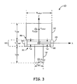
- Figure 3 is a side view of the waveguide system 10 as viewed along the y axis.
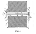
- Figure 4 is a first cross-sectional side view of the waveguide system 10 of Figures 1 and 2A .
- Figure 4 is a second cross-sectional side view of the waveguide system 10 of Figures 1 and 2A .
- the plane upon which the cross-section view of Figure 5 is taken is indicated by section line 5-5 in Figure 2A .
- the "compact interfacing device 100" is also referred to herein as "compact twist 100".
- the compact interfacing device 100 includes a frame 105, a support bar 110, and a dipole bar 115.
- the support bar 110 extends between and is connected to opposing sides 105-1 and 105-2 ( Figure 2B ) of the frame 105.
- a first end 110-1 of the support bar 110 connects to the side 105-1 of the frame 105.
- a second end 110-2 of the support bar 110 connects to the side 105-2 of the frame 105.
- the support bar 110 has a support-bar length L SB ( Figures 2A , 2B , and 4 ) and a support-bar thickness t SB ( Figures 3 and 4 ).
- the dipole bar 115 is orientated orthogonal to the support bar 110 and has a dipole-bar thickness t DB ( Figures 3 and 5 ) and a dipole-bar length L DB ( Figures 2A , 2B , and 5 ) that is less than the support-bar length L SB . As shown in Figure 2B , the dipole bar 115 intersects the support bar 110 at half the support-bar length L SB . Likewise, the support bar 110 intersects the dipole bar 115 at half the dipole-bar length L DB .
- the dipole bar 115 is formed from a conductive material such as metal or plastic coated with metal.
- the dipole-bar length L DB of the dipole bar 115 is on the order of half a wavelength ⁇ of the EM radiation that is rotated by the compact interfacing device 100.
- the signal incident on the dipole bar 115 from the input waveguide 130 induces an alternating current on the dipole bar 115, which is, in turn, coupled from the dipole bar 115 to the output waveguide 140.
- the frame 105 encircles an interior space represented generally at 200 ( Figs 2A and 2B ).
- the interior space 200 is divided in half by the support bar 110.
- the support bar 100 divides the interior space 200 into a first space represented generally at 202 and a second space represented generally at 204 ( Figure 2B ).
- the support bar 100 forms two approximately equal open areas 202 and 204 in the frame 105 on opposite sides of the support bar 100.
- the two open areas 202 and 204 are each partially bisected by respective portions of the dipole bar 115.
- the first open area 202 (first space 202) is partially bisected by the first portion 115-1 of the dipole bar 115
- the second open area 204 (second space 204) is partially bisected by the second portion 115-2 of the dipole bar 115.
- the interior space 200 of the frame 105 includes an insertion region 151 ( Figures 4 and 5 ) on a first side 116 of the dipole bar 115 and on a first side 111 of the support bar 110.
- the interior space 200 of the frame 105 includes an exit region 152 ( Figures 4 and 5 ) on a second side 117 of the dipole bar 115 and on a second side 112 of the support bar 110.
- the second side 117 of the dipole bar 115 opposes the first side 116 of the dipole bar 115.
- the second side 112 of the support bar 110 opposes the first side 111 of the support bar 110.
- the compact interfacing device 100 also includes flanges 301 and 302, which are only shown in Figures 4 and 5 to reduce the complexity of Figures 1 , 2A , and 3 .
- the compact interfacing device 100 includes a first flange 301 to position an output-face of the input waveguide 130 at the input-side represented generally at 351 of the frame 105.
- the compact interfacing device 100 includes a second flange 302 to position an input-face of the output waveguide 140 at an output-side represented generally at 352 of the frame 105. In this manner, the input waveguide 130 interfaces an input-side 351 of the frame 105 and the output waveguide 140 interfaces an output-side 352 of the frame 105.
- the input waveguide 130 has an input width W input , a thickness t input , and a length L IWG .
- the width W input has an extent that is parallel to the y axis shown in Figures 1 , 2A , and 3 .
- the thickness t input has an extent that is parallel to the x axis shown in Figures 1 , 2A , and 3 .
- the length L IWG has an extent that is parallel to the z axis.
- the output waveguide 140 has an output width W output , a thickness t output , and a length L OWG .
- the width W output has an extent that is parallel to the x axis shown in Figures 1 , 2A , and 3 .
- the thickness t output has an extent that is parallel to the y axis shown in Figures 1 , 2A , and 3 .
- the length L OWG has an extent that is parallel to the z axis.
- the waveguide system 10 is operably configured as shown in Figure 2A to rotate an EM field by twice the angle ⁇ 1 .
- the compact interfacing device 100 is configured to rotate electro-magnetic fields (E input -H input and E output -H output ) between the input waveguide 130 and the orthogonally arranged output waveguide 140.
- the compact interfacing device 100 inputs electro-magnetic fields E input -H input from an input waveguide 130, and rotates the input electro-magnetic fields E input -H input by 90 degrees, so that output electro-magnetic fields E output -H output are coupled to an orthogonally arranged output waveguide 140.
- the length L SB of the support bar 110 has an extent that is at an angle ⁇ 1 with reference to the y axis and the length L DB of the dipole bar 115 has an extent that is at an angle - ⁇ 1 with reference to the y axis.
- the input width W input of the input waveguide 130 is arranged so that an extent of the input width W input is orientated at a first angle - ⁇ 1 with respect to an extent (dipole-bar length L DB ) of the dipole bar 115.
- the angle ⁇ 1 is 45 degrees and the angle - ⁇ 1 is -45 degrees (the negative of the angle of ⁇ 1 degrees).
- the E-field E input propagating within the input waveguide 130 is oriented parallel to the x axis (e.g., parallel to the extent of the input thickness t input of the input waveguide 130).
- the E-field E input is input to the compact interfacing device 100 with an orientation of 45 degrees to the extent of the support-bar length L SB of the support bar 110 and with an orientation of 45 degrees to the extent of support-bar length L DB of the dipole bar 115.
- the input EM radiation (E input -H input ) propagates in the z direction toward the input side 351 ( Figures 3 and 5 ) of the compact twist 100.
- the input magnetic field (H input ) in input to the compact interfacing device 100.
- the compact twist 100 causes a 90 degree rotation (i.e., a rotation of twice the orientation of 45 degrees to the extent of the dipole-bar length L SB ) of the input magnetic field (H input ) so that the output magnetic field (H output ) is coupled to the output waveguide 140.
- the output EM radiation propagates in the z direction away from the output side 352 ( Figures 3 and 5 ) of the compact twist 100.
- the output waveguide 140 supports propagation of the output magnetic field (H output ) that is aligned parallel to the extent of the output thickness t output of the output waveguide 140.
- the support-bar thickness t SB is about equal to the dipole-bar thickness t DB and the frame thickness t f is greater than the support-bar thickness t SB and the dipole-bar thickness t DB .
- the frame thickness t f is an insertion length of the compact interfacing device 100 for rotating electro-magnetic fields.
- the dipole-bar thickness t DB is much less than input width W input of the input waveguide 130 and the output width W output of the output waveguide 140.
- the input width W input of the input waveguide 130 is about equal to the output width W output of the output waveguide 140.
- the input waveguide 130 is a single mode waveguide.
- the output waveguide 140 is a single mode waveguide.
- Figure 6 is an oblique view of one embodiment of a compact interfacing device 101 to rotate electro-magnetic fields by 2 ⁇ 3 for coupling from an input waveguide 130 and to an output waveguide 140 that is arranged with an orientation of 2 ⁇ 3 in accordance with the present invention.
- an extent of the width W input of the input waveguide 130 is arranged at an angle ⁇ 3 degrees from the extent of the dipole bar 115 and the extent of the width W output of the output waveguide 140 is arranged at an angle - ⁇ 3 degrees (the negative of the angle of ⁇ 3 degrees) from the extent of the dipole bar 115.
- the compact interfacing device 101 inputs electro-magnetic fields E input -H input from an input waveguide 130, and rotates the input electro-magnetic fields E input -H input by twice ⁇ 3 degrees, so that output electro-magnetic fields E output -H output are coupled to an output waveguide 140 that has a width W output that is orientated at 2 ⁇ 3 degrees from the width W input of the input waveguide 130.
- the angle ⁇ 3 or - ⁇ 3 degrees is always measured from the extent of the dipole bar 115 and the absolute value of ⁇ 3 is greater than 0 degrees and less than 90 degrees.
- Figure 7 is a flow diagram of a method 700 of making a compact interfacing device 100.
- Block 702 is optional.
- the dimensions of a compact interfacing device 100 are optimized for the frequency of operation. The optimizing can be done either empirically or by modeling. Method 700 is described with reference to Figure 2B .
- two open areas 202 and 204 are formed are in a frame 105 on opposite sides of a support bar having two ends connected to the frame 105.
- the two open areas 202 and 204 are partially bisected by respective portions 115-1 and 115-2 of a dipole bar 115.
- forming two open areas 202 and 204 in the frame 105 partially bisected by the dipole bar 115 includes machining a metal disc to form the two open areas partially bisected by the respective portions of the dipole bar.
- forming two open areas 202 and 204 in the frame 105 partially bisected by the dipole bar 115 includes forming a mold configured to form the frame, the support bar, and the dipole bar orientated orthogonal to the support bar. Then molten plastic is forced into the mold to form the frame, the support bar, and the dipole bar. The plastic is released from the mold after the plastic has set. The molded plastic is coated with metal. In this embodiment, the blocks 704 and 706 occur at the same time since the two open areas 202 and 204 are formed at about the same time as the portions 115-1 and 115-2 of the dipole bar 115 are formed.
- forming two open areas 202 and 204 in the frame 105 partially bisected by the dipole bar 115 includes printing the frame, the support bar, and the dipole bar in three dimensions (3D) in metal.
- forming two open areas 202 and 204 in the frame 105 partially bisected by the dipole bar 115 includes printing the frame, the support bar, and the dipole bar in three dimensions (3D) in plastic.
- the printed plastic frame, the plastic support bar, and the plastic dipole bar are coated with metal.
- FIG 8 is an oblique view of one embodiment of a compact interfacing device 101 in accordance with the present invention.
- the compact interfacing device 101 is formed within a support structure 85.
- the frame 105 is suspended (suspension features not shown) inside the support structure 85 with an open area 95 at least partially surrounding the the compact interfacing device 100.
- the frame 105 is part of the support structure 85.
- Studs 96-1 and 96-2 are alignment pins for the input waveguide 130 and the output waveguide 140.
- Flange holes 97 are also used to aide in the alignment of the input waveguide 130 and the output waveguide 140 to the compact interfacing device 100.
Landscapes
- Waveguide Aerials (AREA)
- Optical Integrated Circuits (AREA)
- Waveguides (AREA)
Description
- In the packaging of a waveguide system it is sometimes necessary to change the axial orientation of the waveguide by 90 degrees along the length of a waveguide run. For example, the axial orientation of the waveguide may be required to change from an H-plane orientation to an E-plane orientation or the other way around. For a linearly-polarized antenna, an E-plane is the plane containing the electric field vector in the direction of maximum radiation. An H-plane is the plane containing the magnetic field vector in the direction of maximum radiation. The magnetizing field or H-plane is orthogonal to the E-plane.
- The electric field or E-plane determines the polarization and orientation of the radio wave. For a vertically-polarized antenna, the E-plane usually coincides with the vertical/elevation plane and the H-plane coincides with the horizontal/azimuth plane. For a horizontally-polarized antenna, the E-plane usually coincides with the horizontal/azimuth plane and the H-plane coincides with the vertical/elevation plane.
-
US 2004/0246062 discloses a waveguide unit including a vertically polarised waveguide, a horizontally polarised waveguide, and a waveguide type-polarised wave converter interposed between said waveguides. The waveguide type-polarised wave converter has a slit, the shape of which being a combination of two quadrate parts and a connecting part for connecting the two quadrate parts. - Some systems require the rotation of the electro-magnetic fields from an H-plane orientation to an E-plane orientation. A twist or rotation of the E-field is done by a waveguide that physically forces the rotation of the orientation of the E-field (and H-field) by 90 degrees as the electro-magnetic (EM) radiation propagates along the length of the waveguide. A waveguide that physically forces the rotation of the E-field orientation requires a relatively long waveguide length.
- Some systems, such as a power dividing network for an antenna array, require the rotation from an H-plane orientation to an E-plane orientation to occur over a very short distance so the twist (rotation of the E-field) occurs in the shortest length possible. Some shorter length twists are currently available. In one example, a quarter wavelength section orientated at 45 degrees is placed between the orthogonal waveguides. In another example, a resonant iris orientated at 45 degrees is placed between the orthogonal waveguides. A resonant iris can take various forms but is typically an approximately half wavelength slot at the desired frequency, separating the input and output sections of waveguide. Both the quarter wavelength section and the resonant iris have a narrow bandwidth and are sensitive to bandwidth. A resonant iris is also sensitive to machining tolerances due to narrow gaps in the iris.
- The present application relates to a compact interfacing device for rotating electro-magnetic fields between an input waveguide and an output waveguide. The interfacing device includes a support bar extending between and connected to opposing sides of a frame. The support bar has a support-bar length and a support-bar thickness. The frame encircles an interior space divided by the support bar. The frame has a frame thickness. The interfacing device also includes a dipole bar orientated orthogonal to the support bar. The dipole bar has a dipole-bar thickness and a dipole-bar length that is less than the support-bar length. When the input waveguide interfaces an input-side of the frame and is arranged so that an extent of an input width of the input waveguide is orientated at first angle with respect to an extent of the dipole-bar length, and when the output waveguide interfaces an output-side of the frame and is arranged so that an extent of an output width of the output waveguide is orientated at a second angle with respect to the extent of the dipole-bar length, an input electric field aligned perpendicular to the extent of the input width is rotated upon propagating through the compact interfacing device so that an output electric field aligned perpendicular to the extent of the output width is coupled to the output waveguide. The second angle is equal to and opposite the first angle.
-
-
Figure 1 is an oblique view of one embodiment of a waveguide system including a compact interfacing device, an input waveguide, and an orthogonally arranged output waveguide in accordance with the present invention; -
Figure 2A is a top view of the waveguide system ofFigure 1 ; -
Figure 2B is a top view of the compact interfacing device ofFigure 1 ; -
Figures 3-5 are various side views of the waveguide system ofFigure 1 ; -
Figure 6 is a top view of one embodiment of a waveguide system including compact interfacing device, an input waveguide, and an output waveguide in accordance with the present invention; -
Figure 7 is a flow diagram of one embodiment of a method to make a compact interfacing device in accordance with the present invention; and -
Figure 8 is an oblique view of one embodiment of a compact interfacing device in accordance with the present invention. - In accordance with common practice, the various described features are not drawn to scale but are drawn to emphasize features relevant to the present invention. Like reference characters denote like elements throughout figures and text.
- In the following detailed description, reference is made to the accompanying drawings that form a part hereof, and in which is shown by way of illustration specific illustrative embodiments in which the invention may be practiced. These embodiments are described in sufficient detail to enable those skilled in the art to practice the invention, and it is to be understood that other embodiments may be utilized and that changes may be made without departing from the scope of the present invention. The following detailed description is, therefore, not to be taken in a limiting sense.
- The "compact interfacing device" described herein is also referred to herein as a "compact twist". In one embodiment, the compact twist is operably positioned between an input waveguide and an orthogonally arranged output waveguide to rotate electro-magnetic fields over a short distance so as to couple electro-magnetic radiation emitted from an H-plane orientated input waveguide to a E-plane orientated output waveguide (or vice versa). This rotation of the EM radiation is referred to herein as a twisting of the EM fields. In another implementation of this embodiment, the compact twist is operably positioned between an input waveguide and an output waveguide arranged with an angle θ between the largest extend of the input and output waveguides, so that the compact twist rotates electro-magnetic fields by the angle θ over a short distance. In one implementation of this embodiment, the compact twist is operably positioned between an input waveguide and an output waveguide arranged at an angle, θ, with respect to each other, where θ does not equal either 0 degrees or 90 degrees. In this latter case, the compact twist is operable to rotate electro-magnetic fields by the angle θ over a short distance. This embodiment is described below with reference to
Figure 6 . - As defined herein, "a short distance" is either: much less than the shortest dimension of the input waveguide supporting the electro-magnetic radiation incident on and rotated by the compact twist; or much less than a quarter of the guided wavelength. In one implementation of this embodiment, a short distance is 25% less than the shortest dimension of the input waveguide supporting the electro-magnetic radiation incident on and rotated by the compact twist. In another implementation of this embodiment, a short distance is 25% less than a quarter of the guided wavelength. In yet another implementation of this embodiment, a short distance is 10% less than the shortest dimension of the input waveguide supporting the electro-magnetic radiation incident on and rotated by the compact twist. In yet another implementation of this embodiment, a short distance is 10% less than a quarter of the guided wavelength.
-
Figure 1 is an oblique view of one embodiment of awaveguide system 10 including acompact interfacing device 100, aninput waveguide 130, and an orthogonally arrangedoutput waveguide 140 in accordance with the present invention.Figure 2A is a top view of the waveguide system ofFigure 1 .Figure 2B is a top view of the compact interfacing device ofFigure 1 . Theinput waveguide 130 and theoutput waveguide 140 are not shown inFigure 2B .Figures 3-5 are various side views of the waveguide system ofFigure 1 .Figure 3 is a side view of thewaveguide system 10 as viewed along the y axis.Figure 4 is a first cross-sectional side view of thewaveguide system 10 ofFigures 1 and2A . The plane upon which the cross-section view ofFigure 4 is taken is indicated by section line 4-4 inFigure 2A .Figure 5 is a second cross-sectional side view of thewaveguide system 10 ofFigures 1 and2A . The plane upon which the cross-section view ofFigure 5 is taken is indicated by section line 5-5 inFigure 2A . The "compact interfacing device 100" is also referred to herein as "compact twist 100". - The
compact interfacing device 100 includes aframe 105, asupport bar 110, and adipole bar 115. Thesupport bar 110 extends between and is connected to opposing sides 105-1 and 105-2 (Figure 2B ) of theframe 105. A first end 110-1 of thesupport bar 110 connects to the side 105-1 of theframe 105. A second end 110-2 of thesupport bar 110 connects to the side 105-2 of theframe 105. Thesupport bar 110 has a support-bar length LSB (Figures 2A ,2B , and4 ) and a support-bar thickness tSB (Figures 3 and4 ). - The
dipole bar 115 is orientated orthogonal to thesupport bar 110 and has a dipole-bar thickness tDB (Figures 3 and5 ) and a dipole-bar length LDB (Figures 2A ,2B , and5 ) that is less than the support-bar length LSB. As shown inFigure 2B , thedipole bar 115 intersects thesupport bar 110 at half the support-bar length LSB. Likewise, thesupport bar 110 intersects thedipole bar 115 at half the dipole-bar length LDB. Thedipole bar 115 is formed from a conductive material such as metal or plastic coated with metal. The dipole-bar length LDB of thedipole bar 115 is on the order of half a wavelength λ of the EM radiation that is rotated by thecompact interfacing device 100. The EM radiation incident on thedipole bar 115 causes the free electrons in thedipole bar 115 to oscillate. Specifically, when EM radiation with a wavelength of about λ= 2 LDB is incident on thedipole bar 115, the incident radiation generates an alternating current I = I0eiω in thedipole bar 115, where ω=2πf is the angular frequency, and the EM wavelength is λ=c/f. The signal incident on thedipole bar 115 from theinput waveguide 130 induces an alternating current on thedipole bar 115, which is, in turn, coupled from thedipole bar 115 to theoutput waveguide 140. - The
frame 105 encircles an interior space represented generally at 200 (Figs 2A and2B ). Theinterior space 200 is divided in half by thesupport bar 110. As shown inFigure 2B , thesupport bar 100 divides theinterior space 200 into a first space represented generally at 202 and a second space represented generally at 204 (Figure 2B ). Thus, thesupport bar 100 forms two approximately equalopen areas frame 105 on opposite sides of thesupport bar 100. The twoopen areas dipole bar 115. Specifically, the first open area 202 (first space 202) is partially bisected by the first portion 115-1 of thedipole bar 115 and the second open area 204 (second space 204) is partially bisected by the second portion 115-2 of thedipole bar 115. - The
interior space 200 of theframe 105 includes an insertion region 151 (Figures 4 and5 ) on afirst side 116 of thedipole bar 115 and on afirst side 111 of thesupport bar 110. Theinterior space 200 of theframe 105 includes an exit region 152 (Figures 4 and5 ) on asecond side 117 of thedipole bar 115 and on asecond side 112 of thesupport bar 110. Thesecond side 117 of thedipole bar 115 opposes thefirst side 116 of thedipole bar 115. Thesecond side 112 of thesupport bar 110 opposes thefirst side 111 of thesupport bar 110. - In one implementation of this embodiment, the
compact interfacing device 100 also includesflanges Figures 4 and5 to reduce the complexity ofFigures 1 ,2A , and3 . As shown inFigures 4 and5 , thecompact interfacing device 100 includes afirst flange 301 to position an output-face of theinput waveguide 130 at the input-side represented generally at 351 of theframe 105. Thecompact interfacing device 100 includes asecond flange 302 to position an input-face of theoutput waveguide 140 at an output-side represented generally at 352 of theframe 105. In this manner, theinput waveguide 130 interfaces an input-side 351 of theframe 105 and theoutput waveguide 140 interfaces an output-side 352 of theframe 105. - The
input waveguide 130 has an input width Winput, a thickness tinput, and a length LIWG. The width Winput has an extent that is parallel to the y axis shown inFigures 1 ,2A , and3 . The thickness tinput has an extent that is parallel to the x axis shown inFigures 1 ,2A , and3 . The length LIWG has an extent that is parallel to the z axis. - The
output waveguide 140 has an output width Woutput, a thickness toutput, and a length LOWG. The width Woutput has an extent that is parallel to the x axis shown inFigures 1 ,2A , and3 . The thickness toutput has an extent that is parallel to the y axis shown inFigures 1 ,2A , and3 . The length LOWG has an extent that is parallel to the z axis. - The
waveguide system 10 is operably configured as shown inFigure 2A to rotate an EM field by twice the angle θ1. Thecompact interfacing device 100 is configured to rotate electro-magnetic fields (Einput-Hinput and Eoutput-Houtput) between theinput waveguide 130 and the orthogonally arrangedoutput waveguide 140. Specifically, thecompact interfacing device 100 inputs electro-magnetic fields Einput-Hinput from aninput waveguide 130, and rotates the input electro-magnetic fields Einput-Hinput by 90 degrees, so that output electro-magnetic fields Eoutput-Houtput are coupled to an orthogonally arrangedoutput waveguide 140. - As shown in
Figure 2A , the length LSB of thesupport bar 110 has an extent that is at an angle θ1 with reference to the y axis and the length LDB of thedipole bar 115 has an extent that is at an angle -θ1 with reference to the y axis. As shown inFigure 2A , the input width Winput of theinput waveguide 130 is arranged so that an extent of the input width Winput is orientated at a first angle -θ1 with respect to an extent (dipole-bar length LDB) of thedipole bar 115. The output width Woutput of theoutput waveguide 140 is arranged so that an extent of the output width Woutput is orientated at a second angle θ2 = θ1 with respect to the extent (dipole-bar length LDB) of thedipole bar 115. - In the exemplary embodiment shown in
Figure 2A , the angle θ1 is 45 degrees and the angle -θ1 is -45 degrees (the negative of the angle of θ1 degrees). As shown inFigures 1 ,2A , and3 , the E-field Einput propagating within theinput waveguide 130 is oriented parallel to the x axis (e.g., parallel to the extent of the input thickness tinput of the input waveguide 130). Thus, as shown inFigures 1 ,2A , and3 , the E-field Einput is input to thecompact interfacing device 100 with an orientation of 45 degrees to the extent of the support-bar length LSB of thesupport bar 110 and with an orientation of 45 degrees to the extent of support-bar length LDB of thedipole bar 115. - The input EM radiation (Einput-Hinput) propagates in the z direction toward the input side 351 (
Figures 3 and5 ) of thecompact twist 100. The input magnetic field (Hinput) in input to thecompact interfacing device 100. Thecompact twist 100 causes a 90 degree rotation (i.e., a rotation of twice the orientation of 45 degrees to the extent of the dipole-bar length LSB) of the input magnetic field (Hinput) so that the output magnetic field (Houtput) is coupled to theoutput waveguide 140. - The output EM radiation (Eoutput-Houtput) propagates in the z direction away from the output side 352 (
Figures 3 and5 ) of thecompact twist 100. Theoutput waveguide 140 supports propagation of the output magnetic field (Houtput) that is aligned parallel to the extent of the output thickness toutput of theoutput waveguide 140. - In one implementation of this embodiment, the support-bar thickness tSB is about equal to the dipole-bar thickness tDB and the frame thickness tf is greater than the support-bar thickness tSB and the dipole-bar thickness tDB. The frame thickness tf is an insertion length of the
compact interfacing device 100 for rotating electro-magnetic fields. The dipole-bar thickness tDB is much less than input width Winput of theinput waveguide 130 and the output width Woutput of theoutput waveguide 140. In yet another implementation of this embodiment, the input width Winput of theinput waveguide 130 is about equal to the output width Woutput of theoutput waveguide 140. In yet another implementation of this embodiment, theinput waveguide 130 is a single mode waveguide. In yet another implementation of this embodiment, theoutput waveguide 140 is a single mode waveguide. -
Figure 6 is an oblique view of one embodiment of acompact interfacing device 101 to rotate electro-magnetic fields by 2θ3 for coupling from aninput waveguide 130 and to anoutput waveguide 140 that is arranged with an orientation of 2θ3 in accordance with the present invention. As shown inFigure 6 , an extent of the width Winput of theinput waveguide 130 is arranged at an angle θ3 degrees from the extent of thedipole bar 115 and the extent of the width Woutput of theoutput waveguide 140 is arranged at an angle -θ3 degrees (the negative of the angle of θ3 degrees) from the extent of thedipole bar 115. Thecompact interfacing device 101 inputs electro-magnetic fields Einput-Hinput from aninput waveguide 130, and rotates the input electro-magnetic fields Einput-Hinput by twice θ3 degrees, so that output electro-magnetic fields Eoutput-Houtput are coupled to anoutput waveguide 140 that has a width Woutput that is orientated at 2θ3 degrees from the width Winput of theinput waveguide 130. It is to be noted that the angle θ3 or -θ3 degrees is always measured from the extent of thedipole bar 115 and the absolute value of θ3 is greater than 0 degrees and less than 90 degrees. -
Figure 7 is a flow diagram of amethod 700 of making acompact interfacing device 100.Block 702 is optional. Atblock 702, the dimensions of acompact interfacing device 100 are optimized for the frequency of operation. The optimizing can be done either empirically or by modeling.Method 700 is described with reference toFigure 2B . - At
block 704, twoopen areas frame 105 on opposite sides of a support bar having two ends connected to theframe 105. Atblock 706, the twoopen areas dipole bar 115. In one implementation of this embodiment, forming twoopen areas frame 105 partially bisected by thedipole bar 115 includes machining a metal disc to form the two open areas partially bisected by the respective portions of the dipole bar. - In another implementation of this embodiment, forming two
open areas frame 105 partially bisected by thedipole bar 115 includes forming a mold configured to form the frame, the support bar, and the dipole bar orientated orthogonal to the support bar. Then molten plastic is forced into the mold to form the frame, the support bar, and the dipole bar. The plastic is released from the mold after the plastic has set. The molded plastic is coated with metal. In this embodiment, theblocks open areas dipole bar 115 are formed. - In yet another implementation of this embodiment, forming two
open areas frame 105 partially bisected by thedipole bar 115 includes printing the frame, the support bar, and the dipole bar in three dimensions (3D) in metal. - In yet another implementation of this embodiment, forming two
open areas frame 105 partially bisected by thedipole bar 115 includes printing the frame, the support bar, and the dipole bar in three dimensions (3D) in plastic. The printed plastic frame, the plastic support bar, and the plastic dipole bar are coated with metal. -
Figure 8 is an oblique view of one embodiment of acompact interfacing device 101 in accordance with the present invention. As shown inFigure 8 , thecompact interfacing device 101 is formed within asupport structure 85. Theframe 105 is suspended (suspension features not shown) inside thesupport structure 85 with anopen area 95 at least partially surrounding the thecompact interfacing device 100. In one implementation of this embodiment, theframe 105 is part of thesupport structure 85. Studs 96-1 and 96-2 are alignment pins for theinput waveguide 130 and theoutput waveguide 140. Flange holes 97 are also used to aide in the alignment of theinput waveguide 130 and theoutput waveguide 140 to thecompact interfacing device 100. -
- Example 1 includes a compact interfacing device for rotating electro-magnetic fields between an input waveguide and an output waveguide, the interfacing device comprising: a support bar extending between and connected to opposing sides of a frame, the support bar having a support-bar length and a support-bar thickness; the frame encircling an interior space divided by the support bar, the frame having a frame thickness; and a dipole bar orientated orthogonal to the support bar, the dipole bar having a dipole-bar thickness and a dipole-bar length that is less than the support-bar length, wherein when the input waveguide interfaces an input-side of the frame and is arranged so that an extent of an input width of the input waveguide is orientated at first angle with respect to an extent of the dipole-bar length, and when the output waveguide interfaces an output-side of the frame and is arranged so that an extent of an output width of the output waveguide is orientated at a second angle with respect to the extent of the dipole-bar length, the second angle being equal to and opposite the first angle, an input electric field aligned perpendicular to the extent of the input width is rotated upon propagating through the compact interfacing device so that an output electric field aligned perpendicular to the extent of the output width is coupled to the output waveguide.
- Example 2 includes the compact interfacing device of Example 1, further comprising: a first flange to position an output-face of the input waveguide at the input-side of the frame; and a second flange to position an input-face of the output waveguide at an output side of the frame.
- Example 3 includes the compact interfacing device of any of Examples 1-2, wherein the dipole bar intersects the support bar at half the support-bar length.
- Example 4 includes the compact interfacing device of any of Examples 1-3, wherein the support-bar thickness is about equal to the dipole-bar thickness and wherein the frame thickness is greater than the support-bar thickness and the dipole-bar thickness, wherein the frame thickness is an insertion length of the compact interfacing device for rotating electro-magnetic fields, wherein the dipole-bar thickness is much less than the input width and the output width.
- Example 5 includes the compact interfacing device of any of Examples 1-4, wherein the first angle is 45 degrees and the second angle is -45 degrees.
- Example 6 includes the compact interfacing device of any of Examples 1-5, wherein the dipole-bar length is on the order of half a wavelength of the rotated electro-magnetic fields.
- Example 7 includes the compact interfacing device of any of Examples 1-6, wherein the input width is about equal to the output width.
- Example 8 includes the compact interfacing device of any of Examples 1-7, wherein the input waveguide is a single mode waveguide.
- Example 9 includes the compact interfacing device of any of Examples 1-8, wherein the output waveguide is a single mode waveguide.
- Example 10 includes a method of making a compact interfacing device, the method comprising: forming two open areas in a frame on opposite sides of a support bar having two ends connected to the frame; and partially bisecting the two open areas by respective portions of a dipole bar.
- Example 11 includes the method of Example 10, wherein forming two open areas in the frame comprises: machining a metal disc, to form the two open areas partially bisected by the respective portions of the dipole bar.
- Example 12 includes the method of Example 10, wherein forming two open areas in the frame comprises: forming a mold configured to form the frame, the support bar extending between and connected to opposing sides of the frame, and the dipole bar orientated orthogonal to the support bar, the dipole bar being unattached to the frame; forcing molten plastic into the mold to form the frame, the support bar, and the dipole bar; releasing the plastic from the mold after the plastic has set; and coating the molded plastic with metal.
- Example 13 includes the method of Example 10, wherein forming two open areas in the frame comprises: printing the frame, the support bar, and the dipole bar in three dimensions (3D) in metal.
- Example 14 includes the method of Example 10, wherein forming two open areas in the frame comprises: printing the frame, the support bar, and the dipole bar in three dimensions (3D) in plastic; and coating the printed plastic frame, the plastic support bar, and the plastic dipole bar with metal.
- Example 15 includes a waveguide system comprising: an input waveguide configured to support an input electric field propagating along a length of the input waveguide, the input electric field being perpendicular to an extent of an input width of the input waveguide; an output waveguide configured to support an output electric field propagating along a length of the output waveguide, the output electric field being perpendicular to an extent of an output width of the output waveguide, wherein the extent of the input width is orientated at a first angle with respect to the extent of the output width; and a compact interfacing device positioned between the input waveguide and the output waveguide, wherein the compact interfacing device is configured to rotate the input electric field by the first angle, and wherein the compact interfacing device has an insertion length that is much less than the shortest dimension of the input waveguide and much less than the shortest dimension of the output waveguide.
- Example 16 includes the waveguide system of Example 15, wherein interfacing device comprises: a support bar extending between and connected to opposing sides of a frame, the support bar having a support-bar length and a support-bar thickness; a dipole bar orientated orthogonal to the support bar, the dipole bar having a dipole-bar thickness and a dipole-bar length that is less than the support-bar length; and the frame encircling an interior space divided by the support bar, the frame having a frame thickness, wherein the dipole-bar thickness is greater than the support-bar thickness and greater than the frame thickness, wherein when the extent of the input width is orientated at a second angle with respect to an extent of the dipole-bar length, the second angle being half of the first angle, and when the extent of the output width is orientated at the negative of the second angle with respect to the extent of the dipole-bar length, then the input electric field supported in the input waveguide is rotated through the first angle by the interfacing device so that the output electric field is supported in the output waveguide.
- Example 16 includes the waveguide system of Example 15, wherein the interfacing device comprises: a support bar extending between and connected to opposing sides of a frame, the support bar having a support-bar length and a support-bar thickness; a dipole bar orientated orthogonal to the support bar, the dipole bar having a dipole-bar thickness and a dipole-bar length that is less than the support-bar length; and the frame encircling an interior space divided by the support bar, the frame having a frame thickness, wherein the frame thickness is greater than the support-bar thickness and greater than the dipole-bar thickness, wherein when the input waveguide having an input width is arranged so that an extent of the input width is orientated at a second angle with respect to an extent of the dipole-bar length, the second angle being half of the first angle; and when the output waveguide having an output width is arranged so that an extent of the output width is orientated at the opposite of the second angle with respect to the extent of the dipole-bar length, then an input electric field supported in the input waveguide and aligned to propagate perpendicular to the extent of the input width, is coupled to the output waveguide, and wherein an output electric field supported in the output waveguide is aligned to propagate perpendicular to the extent of the output width.
- Example 17 includes the waveguide system of any of Examples 15-16, wherein the interior space of the frame is divided by the support bar into a first open region and a second open region, and wherein a first portion of the dipole bar partially bisects the first open region, and wherein a second portion of the dipole bar partially bisects the second open region.
- Example 18 includes the waveguide system of any of Examples 15-17, wherein the interior space of the frame includes: an insertion region on a first side of the dipole bar and on a first side of the support bar; and an exit region on a second side of the dipole bar and on a second side of the support bar, the second side of the dipole bar opposing the first side of the dipole bar and the second side of the support bar opposing the first side of the support bar.
- Example 19 includes the waveguide system of any of Examples 15-18, wherein the dipole bar intersects the support bar at half the support-bar length.
- Example 20 includes the waveguide system of any of Examples 15-16, wherein the support-bar thickness is much less than the input width and the output width, and wherein the frame thickness is much less than the input width and the output width.
- Although specific embodiments have been illustrated and described herein, it will be appreciated by those of ordinary skill in the art that any arrangement, which is calculated to achieve the same purpose, may be substituted for the specific embodiment shown. This application is intended to cover any adaptations or variations of the present invention. Therefore, it is manifestly intended that this invention be limited only by the claims and the equivalents thereof.
Claims (10)
- A compact interfacing device (100) for rotating electro-magnetic fields (Einput-Hinput, Eoutput-Houtput) between an input waveguide (130) and an output waveguide (140), the interfacing device comprising:a support bar (110) extending between and connected to opposing sides (105-1, 105-2) of a frame (105), the support bar having a support-bar length (LSB) and a support-bar thickness (tSB);the frame (105) encircling an interior space (200) divided by the support bar, the frame having a frame thickness (tf); anda dipole bar (115) orientated orthogonal to the support bar (110), the dipole bar having a dipole-bar thickness (tDB) and a dipole-bar length (LDB) that is less than the support-bar length, whereinwhen the input waveguide (130) interfaces an input-side (351) of the frame and is arranged so that an extent of an input width (Winput) of the input waveguide is orientated at first angle (θ1) with respect to an extent of the dipole-bar length, andwhen the output waveguide (140) interfaces an output-side (352) of the frame and is arranged so that an extent of an output width (Woutput) of the output waveguide is orientated at a second angle (-θ1) with respect to the extent of the dipole-bar length, the second angle (-θ1) being equal to and opposite the first angle (θ1),an input electric field (Einput) aligned perpendicular to the extent of the input width is rotated upon propagating through the compact interfacing device so that an output electric field (Eoutput) aligned perpendicular to the extent of the output width is coupled to the output waveguide.
- The compact interfacing device (100) of claim 1, further comprising:a first flange (301) to position an output-face of the input waveguide (130) at the input-side (351) of the frame (105); anda second flange (302) to position an input-face of the output waveguide (140) at an output side (352) of the frame.
- The compact interfacing device (100) of claim 1, wherein the dipole bar (115) intersects the support bar (110) at half the support-bar length (LSB).
- The compact interfacing device (100) of claim 1, wherein the support-bar thickness (tSB) is about equal to the dipole-bar thickness (tDB) and wherein the frame thickness (tf) is greater than the support-bar thickness (tSB) and the dipole-bar thickness (tDB), wherein the frame thickness is an insertion length (tf) of the compact interfacing device (100) for rotating electro-magnetic fields (Einput-Hinput, Eoutput-Houtput), wherein the dipole-bar thickness is much less than the input width and the output width.
- The compact interfacing device (100) of claim 1, wherein the first angle is 45 degrees and the second angle is -45 degrees.
- The compact interfacing device (100) of claim 1, wherein the dipole-bar length (LDB) is on the order of half a wavelength λ of the rotated electro-magnetic fields (Einput-Hinput, Eoutput-Houtput).
- The compact interfacing device (100) of claim 1, wherein the input width is about equal to the output width.
- The compact interfacing device (100) of claim 1, wherein the input waveguide (130) is a single mode waveguide (130) and the output waveguide (140) is a single mode waveguide.
- A waveguide system (10) including the compact interfacing (100) device of claim 1, the waveguide system (10) comprising:an input waveguide (130) configured to support an input electric field (Einput) propagating along a length (LIWG) of the input waveguide, the input electric field being perpendicular to an extent of an input width (Winput) of the input waveguide;an output waveguide (140) configured to support an output electric field (Eoutput) propagating along a length (LOWG) of the output waveguide, the output electric field being perpendicular to an extent of an output width (Woutput) of the output waveguide, wherein the extent of the input width is orientated at a first angle (2θ3) with respect to the extent of the output width; andthe compact interfacing (100) device positioned between the input waveguide (130) and the output waveguide (140), wherein the compact interfacing device is configured to rotate the input electric field by the first angle (2θ3), and wherein the compact interfacing device has an insertion length (tf) that is much less than the shortest dimension of the input waveguide and much less than the shortest dimension of the output waveguide.
- The waveguide system (10) of claim 9, wherein the interfacing device (100) comprises:a support bar (100) extending between and connected to opposing sides (105-1, 105-2) of a frame (105), the support bar having a support-bar length (LSB) and a support-bar thickness (tSB);a dipole bar (115) orientated orthogonal to the support bar (110), the dipole bar having a dipole-bar thickness (tDB) and a dipole-bar length (LDB) that is less than the support-bar length; andthe frame (105) encircling an interior space (200) divided by the support bar, the frame having a frame thickness (tf), wherein the frame thickness is greater than the support-bar thickness and greater than the dipole-bar thickness, wherein when the extent of the input width (Winput) is orientated at a second angle (θ3) with respect to an extent of the dipole-bar length, the second angle being half of the first angle (2θ3), andwhen the extent of the output width (Woutput) is orientated at the negative of the second angle (-θ3) with respect to the extent of the dipole-bar length,then the input electric field (Einput) supported in the input waveguide (130) is rotated through the first angle (2θ3) by the interfacing device (100) so that the output electric field (Eoutput) is supported in the output waveguide (140).
Applications Claiming Priority (1)
| Application Number | Priority Date | Filing Date | Title |
|---|---|---|---|
| US13/652,684 US9203128B2 (en) | 2012-10-16 | 2012-10-16 | Compact twist for connecting orthogonal waveguides |
Publications (2)
| Publication Number | Publication Date |
|---|---|
| EP2722925A1 EP2722925A1 (en) | 2014-04-23 |
| EP2722925B1 true EP2722925B1 (en) | 2015-01-28 |
Family
ID=48917393
Family Applications (1)
| Application Number | Title | Priority Date | Filing Date |
|---|---|---|---|
| EP13179001.6A Not-in-force EP2722925B1 (en) | 2012-10-16 | 2013-08-01 | Compact twist for connecting orthogonal waveguides |
Country Status (4)
| Country | Link |
|---|---|
| US (1) | US9203128B2 (en) |
| EP (1) | EP2722925B1 (en) |
| JP (1) | JP2014082751A (en) |
| CA (1) | CA2823122A1 (en) |
Families Citing this family (7)
| Publication number | Priority date | Publication date | Assignee | Title |
|---|---|---|---|---|
| US9105952B2 (en) | 2012-10-17 | 2015-08-11 | Honeywell International Inc. | Waveguide-configuration adapters |
| US9406987B2 (en) | 2013-07-23 | 2016-08-02 | Honeywell International Inc. | Twist for connecting orthogonal waveguides in a single housing structure |
| US10056698B2 (en) | 2014-10-20 | 2018-08-21 | Honeywell International Inc. | Multiple beam antenna systems with embedded active transmit and receive RF modules |
| RU2626726C1 (en) * | 2016-07-12 | 2017-07-31 | Акционерное общество "Концерн воздушно-космической обороны "Алмаз-Антей"(АО "Концерн ВКО "Алмаз-Антей") | Compact 90-degree twisting in the rectangular waveguide |
| CN106602194B (en) * | 2016-11-09 | 2022-02-18 | 迈特通信设备(苏州)有限公司 | E-H conversion waveguide device |
| CN115732873B (en) * | 2022-11-17 | 2023-07-21 | 电子科技大学 | An Ultra-Wideband Thin-Plate 90° Twisted Waveguide |
| US12555915B2 (en) | 2024-07-24 | 2026-02-17 | Keysight Technologies, Inc. | Systems and methods for rotating polarization of radio frequency waves |
Family Cites Families (26)
| Publication number | Priority date | Publication date | Assignee | Title |
|---|---|---|---|---|
| US2729794A (en) | 1950-10-20 | 1956-01-03 | Sperry Rand Corp | High frequency apparatus |
| US2975383A (en) | 1957-11-04 | 1961-03-14 | Gen Motors Corp | Waveguide polarization converter |
| JPS60130902A (en) * | 1983-12-19 | 1985-07-12 | Fujitsu Ltd | Dual polarization waveguide |
| DE3537354A1 (en) | 1985-10-19 | 1987-04-23 | Licentia Gmbh | Arrangement for rotating the polarisation plane of electromagnetic waves |
| SE463489B (en) | 1989-04-12 | 1990-11-26 | Ericsson Telefon Ab L M | FAILURING TRANSITIONAL TRANSITION |
| US6087908A (en) | 1998-09-11 | 2000-07-11 | Channel Master Llc | Planar ortho-mode transducer |
| US6031434A (en) | 1998-09-18 | 2000-02-29 | Hughes Electronics Corporation | Coaxially configured OMT-multiplexer assembly |
| US6225875B1 (en) | 1998-10-06 | 2001-05-01 | Hughes Electronics Corporation | Dual sidewall coupled orthomode transducer having septum offset from the transducer axis |
| US6313714B1 (en) | 1999-10-15 | 2001-11-06 | Trw Inc. | Waveguide coupler |
| JP3706522B2 (en) | 2000-02-25 | 2005-10-12 | シャープ株式会社 | Waveguide device for satellite receiving converter |
| DE10032172A1 (en) | 2000-07-01 | 2002-01-17 | Marconi Comm Gmbh | Transition for orthogonally oriented waveguides |
| US6724277B2 (en) | 2001-01-24 | 2004-04-20 | Raytheon Company | Radio frequency antenna feed structures having a coaxial waveguide and asymmetric septum |
| EP1296404A1 (en) | 2001-09-19 | 2003-03-26 | Marconi Communications GmbH | Waveguide twist with orthogonal rotation of both direction and polarisation |
| JP4060228B2 (en) | 2003-04-04 | 2008-03-12 | 三菱電機株式会社 | Waveguide type demultiplexer |
| JP3884725B2 (en) | 2003-06-03 | 2007-02-21 | 三菱電機株式会社 | Waveguide device |
| JP4154535B2 (en) | 2003-10-06 | 2008-09-24 | 株式会社村田製作所 | Twisted waveguide and radio equipment |
| GB2432461A (en) | 2005-11-17 | 2007-05-23 | Marconi Comm Gmbh | T-shape waveguide twist-transformer junction |
| US7656359B2 (en) | 2006-05-24 | 2010-02-02 | Wavebender, Inc. | Apparatus and method for antenna RF feed |
| US7397323B2 (en) | 2006-07-12 | 2008-07-08 | Wide Sky Technology, Inc. | Orthomode transducer |
| FR2904478B1 (en) | 2006-07-28 | 2010-04-23 | Cit Alcatel | ORTHOMODE TRANSDUCTION DEVICE COMPRISING OPTIMIZED IN THE MESH PLAN FOR AN ANTENNA |
| US7847652B1 (en) | 2008-03-27 | 2010-12-07 | Victory Microwave Corporation | Compact orthomode transducer with improved cross-polarization isolation |
| US8013687B2 (en) | 2008-04-04 | 2011-09-06 | Optim Microwave, Inc. | Ortho-mode transducer with TEM probe for coaxial waveguide |
| WO2010061008A1 (en) | 2008-11-03 | 2010-06-03 | Radiacion Y Microondas, S.A. | Compact orthomode transducer |
| EP2214251B1 (en) | 2009-02-02 | 2012-01-18 | Centre National D'etudes Spatiales | A waveguide orthomode transducer |
| ES2425201T3 (en) | 2010-02-16 | 2013-10-14 | Radiacion Y Microondas, S.A. | Bow tie twist with multiple bow-shaped sections |
| US9105952B2 (en) | 2012-10-17 | 2015-08-11 | Honeywell International Inc. | Waveguide-configuration adapters |
-
2012
- 2012-10-16 US US13/652,684 patent/US9203128B2/en active Active
-
2013
- 2013-08-01 EP EP13179001.6A patent/EP2722925B1/en not_active Not-in-force
- 2013-08-06 JP JP2013163141A patent/JP2014082751A/en active Pending
- 2013-08-08 CA CA2823122A patent/CA2823122A1/en not_active Abandoned
Also Published As
| Publication number | Publication date |
|---|---|
| JP2014082751A (en) | 2014-05-08 |
| EP2722925A1 (en) | 2014-04-23 |
| CA2823122A1 (en) | 2014-04-16 |
| US20140104017A1 (en) | 2014-04-17 |
| US9203128B2 (en) | 2015-12-01 |
Similar Documents
| Publication | Publication Date | Title |
|---|---|---|
| EP2722925A1 (en) | Compact twist for connecting orthogonal waveguides | |
| US2455158A (en) | Wave guide coupling device | |
| CN102084540A (en) | Multimode Resonant Filter | |
| US4380014A (en) | Feed horn for reflector antennae | |
| US9105952B2 (en) | Waveguide-configuration adapters | |
| US20110105019A1 (en) | Radio and antenna system and dual-mode microwave coupler | |
| US20190198963A1 (en) | Rf waveguide twist | |
| IT8267377A1 (en) | WAVEGUIDE DEVICE FOR SEPARATION OF RADIO FREQUENCY SIGNALS OF DIFFERENT FREQUENCIES AND POLARIZATIONS | |
| US6577207B2 (en) | Dual-band electromagnetic coupler | |
| US9812748B2 (en) | Twist for connecting orthogonal waveguides in a single housing structure | |
| US4077039A (en) | Launching and/or receiving network for an antenna feedhorn | |
| US20140340165A1 (en) | Ferrite circulator with integrated e-plane transition | |
| IT8349087A1 (en) | MILLIMETRIC WAVE PHASE SHIFT DEVICE. | |
| US4630059A (en) | Four-port network coupling arrangement for microwave antennas employing monopulse tracking | |
| GB1356260A (en) | Tunable microwave filters | |
| EP4121815B1 (en) | Hybrid circulator | |
| JPS6223201A (en) | Twisted waveguide | |
| GB803621A (en) | Improvements in or relating to electromagnetic wave devices | |
| US4907010A (en) | Directionally sensitive receiving antenna employing gyrotropic material | |
| US3089102A (en) | Dual polarized horn | |
| US3154754A (en) | Circuit for distributing power between two mutually orthogonal polarization paths employing a rotatable absorbing strip | |
| CN221666933U (en) | A quick-lock horn antenna laser pointer | |
| JPS5813001A (en) | Directional filter | |
| JPH03253101A (en) | Polarizer/demultiplexer | |
| KR20250061234A (en) | Plasma generator using resonant waveguide capable of bidirectional incident microwave phase change |
Legal Events
| Date | Code | Title | Description |
|---|---|---|---|
| PUAI | Public reference made under article 153(3) epc to a published international application that has entered the european phase |
Free format text: ORIGINAL CODE: 0009012 |
|
| 17P | Request for examination filed |
Effective date: 20130801 |
|
| AK | Designated contracting states |
Kind code of ref document: A1 Designated state(s): AL AT BE BG CH CY CZ DE DK EE ES FI FR GB GR HR HU IE IS IT LI LT LU LV MC MK MT NL NO PL PT RO RS SE SI SK SM TR |
|
| AX | Request for extension of the european patent |
Extension state: BA ME |
|
| GRAP | Despatch of communication of intention to grant a patent |
Free format text: ORIGINAL CODE: EPIDOSNIGR1 |
|
| INTG | Intention to grant announced |
Effective date: 20140929 |
|
| GRAS | Grant fee paid |
Free format text: ORIGINAL CODE: EPIDOSNIGR3 |
|
| GRAA | (expected) grant |
Free format text: ORIGINAL CODE: 0009210 |
|
| AK | Designated contracting states |
Kind code of ref document: B1 Designated state(s): AL AT BE BG CH CY CZ DE DK EE ES FI FR GB GR HR HU IE IS IT LI LT LU LV MC MK MT NL NO PL PT RO RS SE SI SK SM TR |
|
| REG | Reference to a national code |
Ref country code: GB Ref legal event code: FG4D |
|
| REG | Reference to a national code |
Ref country code: CH Ref legal event code: EP |
|
| REG | Reference to a national code |
Ref country code: IE Ref legal event code: FG4D |
|
| REG | Reference to a national code |
Ref country code: DE Ref legal event code: R096 Ref document number: 602013000930 Country of ref document: DE Effective date: 20150312 |
|
| REG | Reference to a national code |
Ref country code: AT Ref legal event code: REF Ref document number: 708585 Country of ref document: AT Kind code of ref document: T Effective date: 20150315 |
|
| REG | Reference to a national code |
Ref country code: AT Ref legal event code: MK05 Ref document number: 708585 Country of ref document: AT Kind code of ref document: T Effective date: 20150128 |
|
| REG | Reference to a national code |
Ref country code: NL Ref legal event code: VDEP Effective date: 20150128 |
|
| REG | Reference to a national code |
Ref country code: FR Ref legal event code: PLFP Year of fee payment: 3 |
|
| REG | Reference to a national code |
Ref country code: LT Ref legal event code: MG4D |
|
| PG25 | Lapsed in a contracting state [announced via postgrant information from national office to epo] |
Ref country code: LT Free format text: LAPSE BECAUSE OF FAILURE TO SUBMIT A TRANSLATION OF THE DESCRIPTION OR TO PAY THE FEE WITHIN THE PRESCRIBED TIME-LIMIT Effective date: 20150128 Ref country code: BG Free format text: LAPSE BECAUSE OF FAILURE TO SUBMIT A TRANSLATION OF THE DESCRIPTION OR TO PAY THE FEE WITHIN THE PRESCRIBED TIME-LIMIT Effective date: 20150428 Ref country code: ES Free format text: LAPSE BECAUSE OF FAILURE TO SUBMIT A TRANSLATION OF THE DESCRIPTION OR TO PAY THE FEE WITHIN THE PRESCRIBED TIME-LIMIT Effective date: 20150128 Ref country code: SE Free format text: LAPSE BECAUSE OF FAILURE TO SUBMIT A TRANSLATION OF THE DESCRIPTION OR TO PAY THE FEE WITHIN THE PRESCRIBED TIME-LIMIT Effective date: 20150128 Ref country code: FI Free format text: LAPSE BECAUSE OF FAILURE TO SUBMIT A TRANSLATION OF THE DESCRIPTION OR TO PAY THE FEE WITHIN THE PRESCRIBED TIME-LIMIT Effective date: 20150128 Ref country code: HR Free format text: LAPSE BECAUSE OF FAILURE TO SUBMIT A TRANSLATION OF THE DESCRIPTION OR TO PAY THE FEE WITHIN THE PRESCRIBED TIME-LIMIT Effective date: 20150128 Ref country code: NO Free format text: LAPSE BECAUSE OF FAILURE TO SUBMIT A TRANSLATION OF THE DESCRIPTION OR TO PAY THE FEE WITHIN THE PRESCRIBED TIME-LIMIT Effective date: 20150428 |
|
| PG25 | Lapsed in a contracting state [announced via postgrant information from national office to epo] |
Ref country code: RS Free format text: LAPSE BECAUSE OF FAILURE TO SUBMIT A TRANSLATION OF THE DESCRIPTION OR TO PAY THE FEE WITHIN THE PRESCRIBED TIME-LIMIT Effective date: 20150128 Ref country code: AT Free format text: LAPSE BECAUSE OF FAILURE TO SUBMIT A TRANSLATION OF THE DESCRIPTION OR TO PAY THE FEE WITHIN THE PRESCRIBED TIME-LIMIT Effective date: 20150128 Ref country code: IS Free format text: LAPSE BECAUSE OF FAILURE TO SUBMIT A TRANSLATION OF THE DESCRIPTION OR TO PAY THE FEE WITHIN THE PRESCRIBED TIME-LIMIT Effective date: 20150528 Ref country code: NL Free format text: LAPSE BECAUSE OF FAILURE TO SUBMIT A TRANSLATION OF THE DESCRIPTION OR TO PAY THE FEE WITHIN THE PRESCRIBED TIME-LIMIT Effective date: 20150128 Ref country code: LV Free format text: LAPSE BECAUSE OF FAILURE TO SUBMIT A TRANSLATION OF THE DESCRIPTION OR TO PAY THE FEE WITHIN THE PRESCRIBED TIME-LIMIT Effective date: 20150128 Ref country code: GR Free format text: LAPSE BECAUSE OF FAILURE TO SUBMIT A TRANSLATION OF THE DESCRIPTION OR TO PAY THE FEE WITHIN THE PRESCRIBED TIME-LIMIT Effective date: 20150429 Ref country code: PL Free format text: LAPSE BECAUSE OF FAILURE TO SUBMIT A TRANSLATION OF THE DESCRIPTION OR TO PAY THE FEE WITHIN THE PRESCRIBED TIME-LIMIT Effective date: 20150128 |
|
| REG | Reference to a national code |
Ref country code: DE Ref legal event code: R097 Ref document number: 602013000930 Country of ref document: DE |
|
| PG25 | Lapsed in a contracting state [announced via postgrant information from national office to epo] |
Ref country code: SK Free format text: LAPSE BECAUSE OF FAILURE TO SUBMIT A TRANSLATION OF THE DESCRIPTION OR TO PAY THE FEE WITHIN THE PRESCRIBED TIME-LIMIT Effective date: 20150128 Ref country code: CZ Free format text: LAPSE BECAUSE OF FAILURE TO SUBMIT A TRANSLATION OF THE DESCRIPTION OR TO PAY THE FEE WITHIN THE PRESCRIBED TIME-LIMIT Effective date: 20150128 Ref country code: EE Free format text: LAPSE BECAUSE OF FAILURE TO SUBMIT A TRANSLATION OF THE DESCRIPTION OR TO PAY THE FEE WITHIN THE PRESCRIBED TIME-LIMIT Effective date: 20150128 Ref country code: RO Free format text: LAPSE BECAUSE OF FAILURE TO SUBMIT A TRANSLATION OF THE DESCRIPTION OR TO PAY THE FEE WITHIN THE PRESCRIBED TIME-LIMIT Effective date: 20150128 Ref country code: DK Free format text: LAPSE BECAUSE OF FAILURE TO SUBMIT A TRANSLATION OF THE DESCRIPTION OR TO PAY THE FEE WITHIN THE PRESCRIBED TIME-LIMIT Effective date: 20150128 |
|
| PLBE | No opposition filed within time limit |
Free format text: ORIGINAL CODE: 0009261 |
|
| STAA | Information on the status of an ep patent application or granted ep patent |
Free format text: STATUS: NO OPPOSITION FILED WITHIN TIME LIMIT |
|
| RAP2 | Party data changed (patent owner data changed or rights of a patent transferred) |
Owner name: HONEYWELL INTERNATIONAL INC. |
|
| 26N | No opposition filed |
Effective date: 20151029 |
|
| PG25 | Lapsed in a contracting state [announced via postgrant information from national office to epo] |
Ref country code: SI Free format text: LAPSE BECAUSE OF FAILURE TO SUBMIT A TRANSLATION OF THE DESCRIPTION OR TO PAY THE FEE WITHIN THE PRESCRIBED TIME-LIMIT Effective date: 20150128 |
|
| PG25 | Lapsed in a contracting state [announced via postgrant information from national office to epo] |
Ref country code: LU Free format text: LAPSE BECAUSE OF FAILURE TO SUBMIT A TRANSLATION OF THE DESCRIPTION OR TO PAY THE FEE WITHIN THE PRESCRIBED TIME-LIMIT Effective date: 20150801 Ref country code: MC Free format text: LAPSE BECAUSE OF FAILURE TO SUBMIT A TRANSLATION OF THE DESCRIPTION OR TO PAY THE FEE WITHIN THE PRESCRIBED TIME-LIMIT Effective date: 20150128 |
|
| PG25 | Lapsed in a contracting state [announced via postgrant information from national office to epo] |
Ref country code: BE Free format text: LAPSE BECAUSE OF FAILURE TO SUBMIT A TRANSLATION OF THE DESCRIPTION OR TO PAY THE FEE WITHIN THE PRESCRIBED TIME-LIMIT Effective date: 20150128 |
|
| REG | Reference to a national code |
Ref country code: IE Ref legal event code: MM4A |
|
| REG | Reference to a national code |
Ref country code: FR Ref legal event code: PLFP Year of fee payment: 4 |
|
| PG25 | Lapsed in a contracting state [announced via postgrant information from national office to epo] |
Ref country code: IE Free format text: LAPSE BECAUSE OF NON-PAYMENT OF DUE FEES Effective date: 20150801 |
|
| PGFP | Annual fee paid to national office [announced via postgrant information from national office to epo] |
Ref country code: DE Payment date: 20160831 Year of fee payment: 4 Ref country code: IT Payment date: 20160831 Year of fee payment: 4 |
|
| PGFP | Annual fee paid to national office [announced via postgrant information from national office to epo] |
Ref country code: FR Payment date: 20160719 Year of fee payment: 4 |
|
| PG25 | Lapsed in a contracting state [announced via postgrant information from national office to epo] |
Ref country code: MT Free format text: LAPSE BECAUSE OF FAILURE TO SUBMIT A TRANSLATION OF THE DESCRIPTION OR TO PAY THE FEE WITHIN THE PRESCRIBED TIME-LIMIT Effective date: 20150128 |
|
| REG | Reference to a national code |
Ref country code: CH Ref legal event code: PL |
|
| PG25 | Lapsed in a contracting state [announced via postgrant information from national office to epo] |
Ref country code: LI Free format text: LAPSE BECAUSE OF NON-PAYMENT OF DUE FEES Effective date: 20160831 Ref country code: CH Free format text: LAPSE BECAUSE OF NON-PAYMENT OF DUE FEES Effective date: 20160831 |
|
| PG25 | Lapsed in a contracting state [announced via postgrant information from national office to epo] |
Ref country code: HU Free format text: LAPSE BECAUSE OF FAILURE TO SUBMIT A TRANSLATION OF THE DESCRIPTION OR TO PAY THE FEE WITHIN THE PRESCRIBED TIME-LIMIT; INVALID AB INITIO Effective date: 20130801 |
|
| PG25 | Lapsed in a contracting state [announced via postgrant information from national office to epo] |
Ref country code: CY Free format text: LAPSE BECAUSE OF FAILURE TO SUBMIT A TRANSLATION OF THE DESCRIPTION OR TO PAY THE FEE WITHIN THE PRESCRIBED TIME-LIMIT Effective date: 20150128 |
|
| REG | Reference to a national code |
Ref country code: DE Ref legal event code: R119 Ref document number: 602013000930 Country of ref document: DE |
|
| GBPC | Gb: european patent ceased through non-payment of renewal fee |
Effective date: 20170801 |
|
| REG | Reference to a national code |
Ref country code: FR Ref legal event code: ST Effective date: 20180430 |
|
| PG25 | Lapsed in a contracting state [announced via postgrant information from national office to epo] |
Ref country code: SM Free format text: LAPSE BECAUSE OF FAILURE TO SUBMIT A TRANSLATION OF THE DESCRIPTION OR TO PAY THE FEE WITHIN THE PRESCRIBED TIME-LIMIT Effective date: 20150128 |
|
| PG25 | Lapsed in a contracting state [announced via postgrant information from national office to epo] |
Ref country code: MK Free format text: LAPSE BECAUSE OF FAILURE TO SUBMIT A TRANSLATION OF THE DESCRIPTION OR TO PAY THE FEE WITHIN THE PRESCRIBED TIME-LIMIT Effective date: 20150128 Ref country code: TR Free format text: LAPSE BECAUSE OF FAILURE TO SUBMIT A TRANSLATION OF THE DESCRIPTION OR TO PAY THE FEE WITHIN THE PRESCRIBED TIME-LIMIT Effective date: 20150128 Ref country code: PT Free format text: LAPSE BECAUSE OF FAILURE TO SUBMIT A TRANSLATION OF THE DESCRIPTION OR TO PAY THE FEE WITHIN THE PRESCRIBED TIME-LIMIT Effective date: 20150128 |
|
| PG25 | Lapsed in a contracting state [announced via postgrant information from national office to epo] |
Ref country code: DE Free format text: LAPSE BECAUSE OF NON-PAYMENT OF DUE FEES Effective date: 20180301 Ref country code: GB Free format text: LAPSE BECAUSE OF NON-PAYMENT OF DUE FEES Effective date: 20170801 |
|
| PG25 | Lapsed in a contracting state [announced via postgrant information from national office to epo] |
Ref country code: FR Free format text: LAPSE BECAUSE OF NON-PAYMENT OF DUE FEES Effective date: 20170831 Ref country code: IT Free format text: LAPSE BECAUSE OF NON-PAYMENT OF DUE FEES Effective date: 20170801 |
|
| PG25 | Lapsed in a contracting state [announced via postgrant information from national office to epo] |
Ref country code: AL Free format text: LAPSE BECAUSE OF FAILURE TO SUBMIT A TRANSLATION OF THE DESCRIPTION OR TO PAY THE FEE WITHIN THE PRESCRIBED TIME-LIMIT Effective date: 20150128 |
|
| P01 | Opt-out of the competence of the unified patent court (upc) registered |
Effective date: 20230525 |