EP2722878A1 - Semiconductor device and method for manufacturing semiconductor device - Google Patents
Semiconductor device and method for manufacturing semiconductor device Download PDFInfo
- Publication number
- EP2722878A1 EP2722878A1 EP12799958.9A EP12799958A EP2722878A1 EP 2722878 A1 EP2722878 A1 EP 2722878A1 EP 12799958 A EP12799958 A EP 12799958A EP 2722878 A1 EP2722878 A1 EP 2722878A1
- Authority
- EP
- European Patent Office
- Prior art keywords
- cooling unit
- semiconductor device
- protruding portion
- semiconductor module
- pipe
- Prior art date
- Legal status (The legal status is an assumption and is not a legal conclusion. Google has not performed a legal analysis and makes no representation as to the accuracy of the status listed.)
- Withdrawn
Links
Images


Classifications
-
- H—ELECTRICITY
- H10—SEMICONDUCTOR DEVICES; ELECTRIC SOLID-STATE DEVICES NOT OTHERWISE PROVIDED FOR
- H10W—GENERIC PACKAGES, INTERCONNECTIONS, CONNECTORS OR OTHER CONSTRUCTIONAL DETAILS OF DEVICES COVERED BY CLASS H10
- H10W40/00—Arrangements for thermal protection or thermal control
- H10W40/40—Arrangements for thermal protection or thermal control involving heat exchange by flowing fluids
- H10W40/47—Arrangements for thermal protection or thermal control involving heat exchange by flowing fluids by flowing liquids, e.g. forced water cooling
-
- H—ELECTRICITY
- H10—SEMICONDUCTOR DEVICES; ELECTRIC SOLID-STATE DEVICES NOT OTHERWISE PROVIDED FOR
- H10W—GENERIC PACKAGES, INTERCONNECTIONS, CONNECTORS OR OTHER CONSTRUCTIONAL DETAILS OF DEVICES COVERED BY CLASS H10
- H10W40/00—Arrangements for thermal protection or thermal control
- H10W40/70—Fillings or auxiliary members in containers or in encapsulations for thermal protection or control
- H10W40/77—Auxiliary members characterised by their shape
- H10W40/778—Auxiliary members characterised by their shape in encapsulations
-
- H—ELECTRICITY
- H10—SEMICONDUCTOR DEVICES; ELECTRIC SOLID-STATE DEVICES NOT OTHERWISE PROVIDED FOR
- H10W—GENERIC PACKAGES, INTERCONNECTIONS, CONNECTORS OR OTHER CONSTRUCTIONAL DETAILS OF DEVICES COVERED BY CLASS H10
- H10W95/00—Packaging processes not covered by the other groups of this subclass
-
- H—ELECTRICITY
- H10—SEMICONDUCTOR DEVICES; ELECTRIC SOLID-STATE DEVICES NOT OTHERWISE PROVIDED FOR
- H10W—GENERIC PACKAGES, INTERCONNECTIONS, CONNECTORS OR OTHER CONSTRUCTIONAL DETAILS OF DEVICES COVERED BY CLASS H10
- H10W74/00—Encapsulations, e.g. protective coatings
- H10W74/10—Encapsulations, e.g. protective coatings characterised by their shape or disposition
- H10W74/111—Encapsulations, e.g. protective coatings characterised by their shape or disposition the semiconductor body being completely enclosed
- H10W74/114—Encapsulations, e.g. protective coatings characterised by their shape or disposition the semiconductor body being completely enclosed by a substrate and the encapsulations
Definitions
- the present invention relates to a semiconductor device and a method for manufacturing the semiconductor device.
- Patent Document 1 Japanese Patent Application Publication Tokkai No. JP2010-62511
- An obj ect of the present invention is to provide a semiconductor device and a method for manufacturing the semiconductor device which are capable of suppressing the deformation of the pipe when performing the resin-molding.
- a protruding portion that protrudes from a side surface of the cooling unit and surrounds the pipe is provided on the side surface of the cooling unit.
- the semiconductor module and the cooling unit when performing the resin-molding, can be resin-molded with these semiconductor module and cooling unit clamped by a mold having aparting surface that is formed along a side surface of the protruding portion. Therefore, the clamping force acting on the pipe can be reduced, then the deformation of the pipe can be suppressed.
- Fig. 1 is a perspective view showing the semiconductor device according to an embodiment 1.
- Fig. 2 is a sectional view taken along a line S2 - S2 of Fig. 1 .
- Fig. 3 is a sectional view taken along a line S3 - S3 of Fig. 1 .
- Fig. 4 is a front view of a cooling unit of the embodiment 1.
- Fig. 5 is a perspective view showing a method for manufacturing the semiconductor device of the embodiment 1.
- a semi conductor device 1 has a power semiconductor module (hereinafter called a semiconductor module) 2, a cooling unit 3 and a resin mold layer 4.
- the semiconductor module 2 forms an upper arm or a lower arm that corresponds to each phase (U-phase, V-phase and W-phase) of an inverter that PWM-controls drive of a three-phase AC motor for travel of a vehicle.
- An upper and lower arm series circuit of an inverter circuit can be formed by a pair of the semiconductor modules 2, and a three-phase inverter circuit can be formed by combination of three pairs of semiconductor modules 2.
- the semiconductor module 2 has, as main components, a board (or a substrate) 5 having a metal pattern, an IGBT (Insulated Gate Bipolar Transistor) chip 6 that is a power semiconductor device, a diode chip 7, a gate terminal 8 and two lead terminals 9 and 10.
- a board (or a substrate) 5 having a metal pattern
- an IGBT (Insulated Gate Bipolar Transistor) chip 6 that is a power semiconductor device
- diode chip 7 a gate terminal 8
- two lead terminals 9 and 10 two lead terminals 9 and 10.
- the IGBT chip 6 and the diode chip 7 are bonded onto the board 5.
- the gate terminal 8 is a terminal that supplies a gate voltage to the IGBT chip 6, and the gate terminal 8 is connected to the IGBT chip 6 by a bonding wire (not shown) .
- the lead terminals 9 and 10 are bonded or joined onto the board 5.
- the gate terminal 8 and the two lead terminals 9 and 10 protrude outwards with respect to the resin mold layer 4.
- the cooling unit 3 is a unit to cool the semiconductor module 2 that generates heat (heats up), by absorbing the heat from the semiconductor module 2.
- the cooling unit 3 has a heat sink 12, a jacket 13 and pipes 14 and 15.
- the heat sink 12 is formed by material having a high heat radiation property, for instance, by aluminium alloy.
- the heat sink 12 has a base portion 16 and a heat radiating fin 17.
- the base portion 16 is formed into a rectangular plate shape.
- the base portion 16 is provided, on a lower surface side thereof, with the heat radiating fin 17 with the heat radiating fin 17 protruding from the lower surface side.
- An upper surface of the base portion 16 is flat, and the base portion 16 is directly joined to the semiconductor module 2.
- the jacket 13 is formed by material having a high heat radiation property, for instance, by aluminium alloy.
- the jacket 13 is formed into a rectangular box shape whose upper side is open.
- An accommodating portion 18 that accommodates therein the heat radiating fin 17 of the heat sink 12 is formed inside the jacket 13.
- a stepped portion 19, on which an outer peripheral edge of the base portion 16 is seated when the heat radiating fin 17 is accommodated in the accommodating portion 18 is provided at an upper end of the accommodating portion 18.
- the pipes 14 and 15 are pipes that cool the heat radiating fin 17 by flowing or circulating a refrigerant into or through the accommodating portion 18 of the heat sink 12.
- the pipes 14 and 15 are fixedly connected to openings 20a and 22a formed on side surfaces 20 and 22 respectively, which are positioned at short-sized sides of four sides of the jacket 13, of four side surfaces 20, 21, 22 and 23 of the jacket 13 by press-fitting or by welding such as brazing.
- Each of the openings 20a and 22a communicates with the accommodating portion 18.
- the pipes 14 and 15 are formed by, for instance, aluminum, stainless alloy or the like.
- the protruding portion 26 is formed into an isosceles trapezoid, awide size of an upper surface 29 of which is longer than a wide size of a lower surface 30 of which.
- the upper surface 29 and the lower surface 30 are formed or arranged parallel to an upper surface 27 andabottom surface 28 of the cooling unit 3 respectively.
- Two side surfaces 31 and 32 of the protruding portion 26 are formed or set so that a width of the protruding portion 26 gradually narrows from the upper surface 27 side toward the bottom surface 28 side of the cooling unit 3.
- a shape of the protruding portion 25 is the same as that of the protruding portion 26.
- the resin mold layer 4 is formed from PPS (poly-phenylene sulfide), epoxy resin or the like.
- the resin mold layer 4 is formed into a box shape that covers the semiconductor module 2 and the cooling unit 3.
- an outer peripheral edge portion of the board 5 of the semiconductor module 2, each of the gate terminal 8 and the lead terminals 9 and 10 of the semiconductor module 2, the pipes 14 and 15 of the cooling unit 3 and the protruding portions 25 and 26 of the cooling unit 3 are exposed from the resin mold layer 4.
- the heat sink 12 is accommodated in the jacket 13 of the cooling unit 3, and is fixed to the jacket 13 by welding such as brazing or by Friction Stir Welding (FSW). Then, the pipes 14 and 15 are fixed to the openings 20a and 22a of the side surfaces 20 and 22 by press-fitting or using a connecting manner such as brazing ( Fig. 5 (a) ). Subsequently, the semiconductor module 2 is joined to the base portion 16 of the heat sink 12 by high temperature soldering ( Fig. 5(b) ).
- the semiconductor module 2 and the cooling unit 3 are clamped by upper and lower molds 33 and 34, and by filling each cavity (each inside space) of the both upper and lower molds 33 and 34 with resin such as PPS (poly-phenylene sulfide) and epoxy resin by infusing the resin from gates 33a and 34a and by hardening the resin, the resin mold layer 4 is formed ( Figs. 5(C) and 5(d) ). Then, finally, by removing the both upper and lower molds 33 and 34, the semiconductor device 1 of the embodiment 1 can be obtained ( Fig. 5(e) ).
- resin such as PPS (poly-phenylene sulfide) and epoxy resin
- the semiconductor device 1 obtained by removing the both upper and lower molds 33 and 34 is trimmed off so that the gate terminal 8 and the lead terminals 9 and 10 are separate from each other and stick out independently of each other from an outer peripheral frame portion of the board 5 (not shown).
- a parting surface 35 of the upper mold 33 is formed substantially flat along a shape of an upper surface of the semiconductor module 2.
- a parting surface 36 of the lower mold 34 sections of the parting surface 36 which correspond to the side surfaces 21 and 23 of the jacket 13 are formed substantially flat along a shape of a lower surface of the semiconductor module 2, and sections of the parting surface 36 which correspond to the side surfaces 20 and 22 of the jacket 13 are formed along the shape of the lower surface of the semiconductor module 2 and shapes of the protruding portions 25 and 26 of the side surfaces 20 and 22.
- the parting surface 36 of the lower mold 34 is provided with recessed portions 37 and 38 which are formed along the both side surfaces 31 and 32 and the lower surface 30 of the protrudingportions 25 and 26.
- Shapes of the recessed portions 37 and 38 are formed or set so as to be slightly smaller than the shapes of the protruding portions 25 and 26.
- the shapes (outside shapes) of the protruding portions 25 and 26 are formed so as to be slightly greater than the shapes of the recessed portions 37 and 38.
- the parting surface (s) of the mold(s) is formed along the outside shape of the pipe. For this reason, the risk of deforming the pipe might arise due to the fact that the clamping force by the upper and lower molds directly acts on the pipe. Since the deformation of the pipe causes the decrease of the cooling efficiency due to the increase of the flow resistance of the pipe, the deformation of the pipe is undesirable.
- the protruding portions 25 and 26 are provided on the side surfaces 20 and 22 of the jacket 13 of the cooling unit 3, then the resin-molding of the semiconductor module and the cooling unit is performed with the protruding portions 25 and 26 fitted to the recessed portions 38 and 37 of the lower mold 34 respectively. That is, by exerting the clamping force by the upper and lower molds 33 and 34 on the protrudingportions 25 and26, it can be possible to prevent the clamping force from directly acting on the pipes 14 and 15 from the upper and lower molds 33 and 34, therefore the deformation of the pipes 14 and 15 can be suppressed.
- the outside shapes of the protruding portions 25 and 26 are formed so as to be greater than the shapes of the recessed portions 37 and 38 of the lower mold 34. Therefore, when clamping the semiconductor module 2 and the cooling unit 3 by the upper and lower molds 33 and 34, the recessed portions 37 and 38 of the parting surface 36 of the lower mold 34 are in absolute contact with or stick firmly to the lower surface 30 and the both side surfaces 31 and 32 of the protruding portions 25 and 26. It is thus possible to suppress the resin leakage and/or the reaching-out of or filling of redundant resin.
- the two side surfaces 31 and 32 of the protruding portions 25 and 26 are formed or set so that the widths of the protruding portions 25 and 26 gradually narrow from the upper surface 27 side toward the bottom surface 28 side of the coolingunit 3, apart of the clamping force of the upper and lower molds 33 and 34 separately acts on the protruding portions 25 and 26 in right and left directions, then adhesion between the recessed portions 38 and 37 of the lower mold 34 and the both side surfaces 31 and 32 of the protruding portions 25 and 26 can be increased.
- the pipes 14 and 15 can be arranged to be offset from a position of each of the gate terminal 8 and the lead terminals 9 and 10. It is therefore possible to improve degree of flexibility in the layout of the pipes 14 and 15 and the gate terminal 8 and the lead terminals 9 and 10.
- the semiconductor device 1 and the method for manufacturing the semiconductor device 1 of the embodiment 1 have the following effects.
- the recessed portions 37 and 38 of the parting surface 36 of the lower mold 34 are in absolute contact with or stick firmly to the lower surface 30 and the both side surfaces 31 and 32 of the protruding portions 25 and 26. It is thus possible to suppress the resin leakage and/or the reaching-out of or filling of redundant resin.
- Fig. 6 is a front view of a cooling unit according to the embodiment 2.
- Fig. 7 is a sectional view taken along a line S7 - S7 of Fig. 6 .
- the same element or the same component as that of the embodiment 1 is indicated by same name of the element or the component using same reference sign.
- the upper surface 29 of the protruding portion 26 is formed or set at the same position as the upper surface 27 of the jacket 13, and the lower surface 30 of the protruding portion 26 is formed or set at the same position as the bottom surface 28 of the jacket 13.
- a groove 41 that surrounds the pipe 15 is formed close to an outer peripheral edge of the protruding portion 26, and an elastic rib (a protruding line) 42 is provided at an outer side of the groove 41 (a groove 41 that surrounds the pipe 15 is formed close to an outer peripheral edge of the protruding portion 26, thereby providing an elastic rib (a protruding line) 42 at an outer side of the groove 41).
- An outside shape of the protruding portion 26 including the elastic rib 42 is set to be greater than the shapes of the recessed portions 37 and 38 of the lower mold 34.
- Abottom surface 41a of the groove 41 is set at a position which is on an inner side of the cooling unit 3 with respect to inner wall surfaces 33b and 34b of the upper and lower molds 33 and 34.
- a shape of the protruding portion 25 is the same as that of the protruding portion 26.
- the elastic rib 42 when clamping the semiconductor module 2 and the cooling unit 3 by the upper and lower molds 33 and 34, by the fact that the elastic rib 42 is elastically deformed within its elastic deforming region, the elastic rib 42 is absolute contact with or sticks firmly to the parting surfaces 35 and 36 of the upper and lower molds 33 and 34. That is, by an elastic force of the elastic rib 42, the elastic rib 42 and the parting surfaces 35 and 36 of the upper and lower molds 33 and 34 are surely contiguous with each other (both areas of the elastic rib 42 and the parting surfaces 35 and 36 of the upper and lower molds 33 and 34 surely touch each other by area contact). It is thus possible to surely suppress the resin leakage and/or the reaching-out of or filling of redundant resin.
- the elastic rib 42 can be elastically deformed throughout the entire circumference of the elastic rib 42, then the elastic rib 42 is absolute contact with or sticks more firmly to the parting surfaces 35 and 36 of the upper and lower molds 33 and 34.
- the elastic rib 42 is elastically deformed during the clamping of the semiconductor module 2 and the cooling unit 3 by the upper and lower molds 33 and 34, then a gap (rattle or backlash) of the mating surfaces between the upper and lower molds 33 and 34 and the semiconductor module 2 also between the upper and lower molds 33 and 34 and the cooling unit 3 is filled or absorbed. It is thus possible to allow relaxation of the dimensional tolerance of the mating surfaces between the upper and lower molds 33 and 34 and the semiconductor module 2 also between the upper and lower molds 33 and 34.
- a groove 41 is formed close to an outer peripheral edge of the protruding portion 25, 26, and an elastic rib 42 is provided at an outer side of the groove 41.
- a bottom surface 41a of the groove 41 is set at a position which is on an inner side of the cooling unit 3 with respect to the inner wall surface 33b, 34b of the mold 33, 34.
- the elastic rib 42 can be elastically deformed throughout the entire circumference of the elastic rib 42, then the elastic rib 42 is absolute contact with or sticks more firmly to the parting surfaces 35 and 36 of the upper and lower molds 33 and 34.
- the shape of the protruding portion is not limited as long as the protruding portion protrudes in the outward direction of the cooling unit and covers the outer peripheries of the pipe.
- it could be only an elastic rib (a protruding line) 43 that surrounds the pipe 14.
- the embodiment 2 shows, as an example, that the bottom surface of the groove is set at the position which is on the inner side of the cooling unit with respect to the inner wall surface of the mold, the bottom surface of the groove could be set at the same position as the inner wall surface of the mold.
- the groove and the elastic rib are formed throughout the entire circumference of the protruding portion.
- the groove and the elastic rib might be formed only at right and left sides of the protruding portion or only at upper and lower sides of the protruding portion.
- Fig. 9 is an example in which groove 44 and 45 and elastic ribs 46 and 47 are provided only on the side surfaces 31 and 32 of the protruding portion 25.
Landscapes
- Cooling Or The Like Of Semiconductors Or Solid State Devices (AREA)
- Encapsulation Of And Coatings For Semiconductor Or Solid State Devices (AREA)
- Structures Or Materials For Encapsulating Or Coating Semiconductor Devices Or Solid State Devices (AREA)
Abstract
Description
- The present invention relates to a semiconductor device and a method for manufacturing the semiconductor device.
- As a related art semiconductor device, a device that is formed as an integral component of a Semiconductor module and a cooling unit by resin-molding has been known. A pipe to circulate a refrigerant through a heat sink inside the cooling unit is provided on a side surface of the cooling unit with the pipe protruding from the side surface of the cooling unit. An example of technique concerning this related art semiconductor device is disclosed in Patent Document 1.
- Patent Document 1: Japanese Patent Application Publication Tokkai No.
JP2010-62511 - In the related art technique described above, when performing the resin-molding of the semiconductor module and the cooling unit, it is required that a parting surface of a mold be formed along an outside shape of the pipe. For this reason, when the semiconductor module and the cooling unit are clamped by the mold during the resin-molding, there is a risk that the pipe will be deformed due to the fact that a clamping force acts on the pipe. The deformation of the pipe causes a decrease of cooling efficiency due to an increase of a flow resistance of the pipe . An obj ect of the present invention is to provide a semiconductor device and a method for manufacturing the semiconductor device which are capable of suppressing the deformation of the pipe when performing the resin-molding.
- To achieve the object, in the present invention, a protruding portion that protrudes from a side surface of the cooling unit and surrounds the pipe is provided on the side surface of the cooling unit.
- Accordingly, in the present invention, when performing the resin-molding, the semiconductor module and the cooling unit can be resin-molded with these semiconductor module and cooling unit clamped by a mold having aparting surface that is formed along a side surface of the protruding portion. Therefore, the clamping force acting on the pipe can be reduced, then the deformation of the pipe can be suppressed.
-
- [
FIGURE 1] Fig. 1 is a perspective view showing a semiconductor device according to an embodiment 1. - [
FIGURE 2] Fig. 2 is a sectional view taken along a line S2 - S2 ofFig. 1 . - [
FIGURE 3] Fig. 3 is a sectional view taken along a line S3 - S3 ofFig. 1 . - [
FIGURE 4] Fig. 4 is a front view of a cooling unit of the embodiment 1. - [
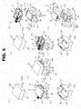
FIGURE 5] Fig. 5 is a perspective view showing a method for manufacturing the semiconductor device of the embodiment 1. - [
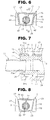
FIGURE 6] Fig. 6 is a front view of a cooling unit according to anembodiment 2. - [
FIGURE 7] Fig. 7 is a sectional view taken along a line s7 - S7 ofFig. 6 . - [
FIGURE 8] Fig. 8 is a front view of a cooling unit, which shows a shape of a protruding portion, according to another embodiment. - [
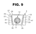
FIGURE 9] Fig. 9 is a front view of a cooling unit, which shows a shape of a protruding portion, according to another embodiment. - In the following description, embodiments of a semiconductor device and a method for manufacturing the semiconductor device of the present invention will be explained with reference to the drawings.
- First, a configuration of the semiconductor device will be explained.
-
Fig. 1 is a perspective view showing the semiconductor device according to an embodiment 1.Fig. 2 is a sectional view taken along a line S2 - S2 ofFig. 1 .Fig. 3 is a sectional view taken along a line S3 - S3 ofFig. 1 .Fig. 4 is a front view of a cooling unit of the embodiment 1.Fig. 5 is a perspective view showing a method for manufacturing the semiconductor device of the embodiment 1. - A semi conductor device 1 has a power semiconductor module (hereinafter called a semiconductor module) 2, a
cooling unit 3 and aresin mold layer 4. - The
semiconductor module 2 forms an upper arm or a lower arm that corresponds to each phase (U-phase, V-phase and W-phase) of an inverter that PWM-controls drive of a three-phase AC motor for travel of a vehicle. An upper and lower arm series circuit of an inverter circuit can be formed by a pair of thesemiconductor modules 2, and a three-phase inverter circuit can be formed by combination of three pairs ofsemiconductor modules 2. - As shown in
Fig. 5 , thesemiconductor module 2 has, as main components, a board (or a substrate) 5 having a metal pattern, an IGBT (Insulated Gate Bipolar Transistor)chip 6 that is a power semiconductor device, adiode chip 7, agate terminal 8 and twolead terminals - The
IGBT chip 6 and thediode chip 7 are bonded onto theboard 5. - The
gate terminal 8 is a terminal that supplies a gate voltage to theIGBT chip 6, and thegate terminal 8 is connected to theIGBT chip 6 by a bonding wire (not shown) . - The
lead terminals board 5. - Here, the
gate terminal 8 and the twolead terminals resin mold layer 4. - The
cooling unit 3 is a unit to cool thesemiconductor module 2 that generates heat (heats up), by absorbing the heat from thesemiconductor module 2. Thecooling unit 3 has aheat sink 12, ajacket 13 andpipes - The
heat sink 12 is formed by material having a high heat radiation property, for instance, by aluminium alloy. Theheat sink 12 has abase portion 16 and aheat radiating fin 17. Thebase portion 16 is formed into a rectangular plate shape. Thebase portion 16 is provided, on a lower surface side thereof, with theheat radiating fin 17 with the heat radiating fin 17 protruding from the lower surface side. An upper surface of thebase portion 16 is flat, and thebase portion 16 is directly joined to thesemiconductor module 2. - The
jacket 13 is formed by material having a high heat radiation property, for instance, by aluminium alloy. Thejacket 13 is formed into a rectangular box shape whose upper side is open. Anaccommodating portion 18 that accommodates therein theheat radiating fin 17 of theheat sink 12 is formed inside thejacket 13. Astepped portion 19, on which an outer peripheral edge of thebase portion 16 is seated when theheat radiating fin 17 is accommodated in theaccommodating portion 18 , is provided at an upper end of theaccommodating portion 18. - The
pipes heat radiating fin 17 by flowing or circulating a refrigerant into or through theaccommodating portion 18 of theheat sink 12. Thepipes openings side surfaces jacket 13, of fourside surfaces jacket 13 by press-fitting or by welding such as brazing. Each of theopenings accommodating portion 18. Thepipes - Protruding
portions cooling unit 3 and cover outer peripheries of thepipes side surfaces jacket 13. - As shown in
Fig. 4 , theprotruding portion 26 is formed into an isosceles trapezoid, awide size of anupper surface 29 of which is longer than a wide size of alower surface 30 of which. Theupper surface 29 and thelower surface 30 are formed or arranged parallel to anupper surface 27andabottom surface 28 of thecooling unit 3 respectively. Two side surfaces 31 and 32 of the protrudingportion 26 are formed or set so that a width of the protrudingportion 26 gradually narrows from theupper surface 27 side toward thebottom surface 28 side of thecooling unit 3. Here, a shape of the protrudingportion 25 is the same as that of the protrudingportion 26. - The
resin mold layer 4 is formed from PPS (poly-phenylene sulfide), epoxy resin or the like. Theresin mold layer 4 is formed into a box shape that covers thesemiconductor module 2 and thecooling unit 3. Here, an outer peripheral edge portion of theboard 5 of thesemiconductor module 2, each of thegate terminal 8 and thelead terminals semiconductor module 2, thepipes cooling unit 3 and the protrudingportions cooling unit 3 are exposed from theresin mold layer 4. - [Method for Manufacturing Semiconductor Device] Next, a method for manufacturing the semiconductor device 1 of the embodiment 1 will be explained with reference to
Fig. 5 . - First, the
heat sink 12 is accommodated in thejacket 13 of thecooling unit 3, and is fixed to thejacket 13 by welding such as brazing or by Friction Stir Welding (FSW). Then, thepipes openings Fig. 5 (a) ). Subsequently, thesemiconductor module 2 is joined to thebase portion 16 of theheat sink 12 by high temperature soldering (Fig. 5(b) ). - Next, the
semiconductor module 2 and thecooling unit 3 are clamped by upper andlower molds lower molds gates resin mold layer 4 is formed (Figs. 5(C) and 5(d) ). Then, finally, by removing the both upper andlower molds Fig. 5(e) ). - Here, the semiconductor device 1 obtained by removing the both upper and
lower molds gate terminal 8 and thelead terminals - Here, as shown in
Fig. 5(c) , aparting surface 35 of theupper mold 33 is formed substantially flat along a shape of an upper surface of thesemiconductor module 2. On the other hand, as for aparting surface 36 of thelower mold 34, sections of theparting surface 36 which correspond to the side surfaces 21 and 23 of thejacket 13 are formed substantially flat along a shape of a lower surface of thesemiconductor module 2, and sections of theparting surface 36 which correspond to the side surfaces 20 and 22 of thejacket 13 are formed along the shape of the lower surface of thesemiconductor module 2 and shapes of the protrudingportions parting surface 36 of thelower mold 34 is provided with recessedportions lower surface 30 of the protrudingportions 25 and 26. Shapes of the recessedportions portions portions portions - Next, function of the present embodiment will be explained.
- In the related art semiconductor device, in the case where the pipe for flowing or circulating the refrigerant is provided on the side surface of the cooling unit, when performing the resin-molding of the semiconductor module and the cooling unit, the parting surface (s) of the mold(s) is formed along the outside shape of the pipe. For this reason, the risk of deforming the pipe might arise due to the fact that the clamping force by the upper and lower molds directly acts on the pipe. Since the deformation of the pipe causes the decrease of the cooling efficiency due to the increase of the flow resistance of the pipe, the deformation of the pipe is undesirable. On the other hand, in a case where the clamping force is decreased to such an extent that the pipe are not deformed, sealing performance is degraded, and a resin leakage and/or reaching-out of or filling of redundant resin occur, then moldability will be deteriorated.
- In contrast to this, in the embodiment 1, the protruding
portions jacket 13 of thecooling unit 3, then the resin-molding of the semiconductor module and the cooling unit is performed with the protrudingportions portions lower mold 34 respectively. That is, by exerting the clamping force by the upper andlower molds protrudingportions 25 and26, it can be possible to prevent the clamping force from directly acting on thepipes lower molds pipes - In the embodiment 1, the outside shapes of the protruding
portions portions lower mold 34. Therefore, when clamping thesemiconductor module 2 and thecooling unit 3 by the upper andlower molds portions parting surface 36 of thelower mold 34 are in absolute contact with or stick firmly to thelower surface 30 and the both side surfaces 31 and 32 of the protrudingportions - Further, since the two
side surfaces portions portions upper surface 27 side toward thebottom surface 28 side of thecoolingunit 3, apart of the clamping force of the upper andlower molds portions portions lower mold 34 and the both side surfaces 31 and 32 of the protrudingportions - [Improvement of Degree of Flexibility in layout] In the case of the related art semiconductor device, it is required that the pipe and each terminal of the semiconductor module be arranged on the parting surface of the mold. That is, it is required that positions of the pipe and each terminal of the semiconductor module be adjusted to heights of the parting surfaces of the upper and lower molds. Thus, a lot of constraints of layout are imposed.
- In contrast to this, in the embodiment 1, since the protruding
portions jacket 13 of thecooling unit 3, thepipes gate terminal 8 and thelead terminals pipes gate terminal 8 and thelead terminals - Next, effects of the present embodiment will be explained.
- The semiconductor device 1 and the method for manufacturing the semiconductor device 1 of the embodiment 1 have the following effects.
- (1) A semiconductor device has: a
semiconductor module 2; acooling unit 3, thesemiconductor module 2 being joined to an upper surface of thecooling unit 3, and apipe side surface cooling unit 3; aresin mold layer 4 that covers outer peripheries of thesemiconductor module 2 and thecooling unit 3; and a protrudingportion side surface cooling unit 3 and protrudes from theside surface cooling unit 3 and surrounds thepipe
With this configuration, the deformation of thepipes
Further, it is possible to improve degree of flexibility in the layout of thepipes gate terminal 8 and thelead terminals - (2) An outside shape of the protruding
portion portion upper surface 27 side toward abottom surface 28 side of thecooling unit 3.
With this structure, the adhesion between the recessedportions lower mold 34 and the both side surfaces 31 and 32 of the protrudingportions - (3) A method for manufacturing a semiconductor device, the semiconductor device being obtained by resin-molding of a
semiconductor module 2 and acooling unit 3, thesemiconductor module 2 being joined to an upper surface of thecooling unit 3, and apipe side surface cooling unit 3, the method has: providing, on theside surface cooling unit 3, a protrudingportion side surface cooling unit 3 and surrounds thepipe semiconductor module 2 and thecooling unit 3 by upper andlower molds surface portion semiconductor module 2 and thecooling unit 3.
With this method, the deformation of thepipes
Further, it is possible to manufacture the semiconductor device that has high degree of flexibility in the layout of thepipes gate terminal 8 and thelead terminals - (4) A shape of the protruding
portion parting surface 36, which corresponds to the protrudingportion lower mold 34. - With this structure, the recessed
portions parting surface 36 of thelower mold 34 are in absolute contact with or stick firmly to thelower surface 30 and the both side surfaces 31 and 32 of the protrudingportions - Next, an
embodiment 2 will be explained with reference toFigs. 6 and 7. Fig. 6 is a front view of a cooling unit according to theembodiment 2.Fig. 7 is a sectional view taken along a line S7 - S7 ofFig. 6 . In theembodiment 2, the same element or the same component as that of the embodiment 1 is indicated by same name of the element or the component using same reference sign. - With regard to the protruding
portion 26, theupper surface 29 of the protrudingportion 26 is formed or set at the same position as theupper surface 27 of thejacket 13, and thelower surface 30 of the protrudingportion 26 is formed or set at the same position as thebottom surface 28 of thejacket 13. - In the
embodiment 2, agroove 41 that surrounds thepipe 15 is formed close to an outer peripheral edge of the protrudingportion 26, and an elastic rib (a protruding line) 42 is provided at an outer side of the groove 41 (agroove 41 that surrounds thepipe 15 is formed close to an outer peripheral edge of the protrudingportion 26, thereby providing an elastic rib (a protruding line) 42 at an outer side of the groove 41). An outside shape of the protrudingportion 26 including theelastic rib 42 is set to be greater than the shapes of the recessedportions lower mold 34. -
Abottom surface 41a of thegroove 41 is set at a position which is on an inner side of thecooling unit 3 with respect to inner wall surfaces 33b and 34b of the upper andlower molds portion 25 is the same as that of the protrudingportion 26. - In the
embodiment 2, since an area of theboard 5 of thepower semiconductor module 2 is set to the substantially same area as thebase portion 16 of theheat sink 12, theboard 5 is not exposed from theresin mold layer 4. - The other element or component and structure of the
embodiment 2 are the same as those of the embodiment 1. - Next, function of the present embodiment will be explained.
- In the
embodiment 2, when clamping thesemiconductor module 2 and thecooling unit 3 by the upper andlower molds elastic rib 42 is elastically deformed within its elastic deforming region, theelastic rib 42 is absolute contact with or sticks firmly to the parting surfaces 35 and 36 of the upper andlower molds elastic rib 42, theelastic rib 42 and the parting surfaces 35 and 36 of the upper andlower molds elastic rib 42 and the parting surfaces 35 and 36 of the upper andlower molds - In addition, since the
bottom surface 41a of thegroove 41 is set at the position which is on the inner side of thecooling unit 3 with respect to the inner wall surfaces 33b and 34b of the upper andlower molds elastic rib 42 can be elastically deformed throughout the entire circumference of theelastic rib 42, then theelastic rib 42 is absolute contact with or sticks more firmly to the parting surfaces 35 and 36 of the upper andlower molds - In general, since a high dimensional accuracy is required for the resin-molding in order that a gap which causes the resin leakage does not appear between the mold and the products, it is necessary to strictly manage or maintain dimensional tolerance of a mating surface with the mold, which might cause a problem of pushing up the cost of manufacturing.
- In contrast to this, in the case of the semiconductor device 1 of the
embodiment 2, theelastic rib 42 is elastically deformed during the clamping of thesemiconductor module 2 and thecooling unit 3 by the upper andlower molds lower molds semiconductor module 2 also between the upper andlower molds cooling unit 3 is filled or absorbed. It is thus possible to allow relaxation of the dimensional tolerance of the mating surfaces between the upper andlower molds semiconductor module 2 also between the upper andlower molds - Accordingly, this can suppress the pushing-up of the cost of manufacturing.
- Next, effects of the present embodiment will be explained.
- In addition to the effects (1) to (4) of the embodiment 1, the semiconductor device 1 and the method for manufacturing the semiconductor device 1 of the
embodiment 2 have the following effects. (5) Agroove 41 is formed close to an outer peripheral edge of the protrudingportion elastic rib 42 is provided at an outer side of thegroove 41. - With this structure, the resin leakage and/or the reaching-out of or filling of redundant resin can be suppressed, and the sealing performance can be improved.
- (6) A
bottom surface 41a of thegroove 41 is set at a position which is on an inner side of thecooling unit 3 with respect to theinner wall surface mold - With this structure, the
elastic rib 42 can be elastically deformed throughout the entire circumference of theelastic rib 42, then theelastic rib 42 is absolute contact with or sticks more firmly to the parting surfaces 35 and 36 of the upper andlower molds - Although the semiconductor device and the method for manufacturing the semiconductor device of the present invention have been described above by reference to certain embodiments of the invention, the present invention is not limited to the embodiments described above. Modifications and variations of the embodiments described above can be possible as the present invention.
- For instance, the shape of the protruding portion is not limited as long as the protruding portion protrudes in the outward direction of the cooling unit and covers the outer peripheries of the pipe. For example, as shown in
Fig. 8 , it could be only an elastic rib (a protruding line) 43 that surrounds thepipe 14. - Although the
embodiment 2 shows, as an example, that the bottom surface of the groove is set at the position which is on the inner side of the cooling unit with respect to the inner wall surface of the mold, the bottom surface of the groove could be set at the same position as the inner wall surface of the mold. - In the
embodiment 2, as an example, the groove and the elastic rib (the protruding line) are formed throughout the entire circumference of the protruding portion. However, the groove and the elastic rib might be formed only at right and left sides of the protruding portion or only at upper and lower sides of the protruding portion.Fig. 9 is an example in whichgroove elastic ribs portion 25. -
- 1
- semiconductor device
- 2
- power semiconductor module
- 3
- cooling unit
- 4
- resin mold layer
- 14, 15
- pipe
- 20, 22
- side surface
- 25, 26
- protruding portion
- 33
- upper mold
- 34
- lower mold
- 35, 36
- parting surface
Claims (6)
- A semiconductor device comprising:a semiconductor module;a cooling unit, the semiconductor module being joined to an upper surface of the cooling unit, and a pipe for circulating a refrigerant being fixed to a side surface of the cooling unit;a resin mold layer that covers outer peripheries of the semiconductor module and the cooling unit; anda protruding portion that is provided on the side surface of the cooling unit and protrudes from the side surface of the cooling unit and surrounds the pipe.
- The semiconductor device as claimed in claim 1, wherein:a groove is formed close to an outer peripheral edge of the protruding portion, anda protruding line is provided at an outer side of the groove.
- The semiconductor device as claimed in claim 1 or 2, wherein:an outside shape of the protruding portion is set so that a width of the protruding portion gradually narrows or widens from an upper surface side toward a bottom surface side of the cooling unit.
- A method for manufacturing a semiconductor device, the semiconductor device being obtained by resin-molding of a semiconductor module and a cooling unit, the semiconductor module being joined to an upper surface of the cooling unit, and a pipe for circulating a refrigerant being fixed to a side surface of the cooling unit, the method comprising:providing, on the side surface of the cooling unit, a protruding portion that protrudes from the side surface of the cooling unit and surrounds the pipe;clamping the semiconductor module and the cooling unit by a mold having a parting surface that is formed along a shape of the protruding portion; andperforming the resin-molding of the semiconductor module and the cooling unit.
- The method for manufacturing the semiconductor device as claimed in claim 4, wherein:a shape of the protruding portion is set to be greater than a shape of the parting surface, which corresponds to the protruding portion, of the mold.
- The method for manufacturing the semiconductor device as claimed in claim 4 or 5, wherein:a groove is formed close to an outer peripheral edge of the protruding portion,a protruding line is provided at an outer side of the groove, anda bottom surface of the groove is set at a same position as an inner wall surface of the mold or at a position which is on an inner side of the cooling unit with respect to the inner wall surface of the mold.
Applications Claiming Priority (2)
| Application Number | Priority Date | Filing Date | Title |
|---|---|---|---|
| JP2011134936A JP5642022B2 (en) | 2011-06-17 | 2011-06-17 | Semiconductor device and manufacturing method of semiconductor device |
| PCT/JP2012/061312 WO2012172875A1 (en) | 2011-06-17 | 2012-04-27 | Semiconductor device and method for manufacturing semiconductor device |
Publications (2)
| Publication Number | Publication Date |
|---|---|
| EP2722878A1 true EP2722878A1 (en) | 2014-04-23 |
| EP2722878A4 EP2722878A4 (en) | 2015-07-29 |
Family
ID=47356871
Family Applications (1)
| Application Number | Title | Priority Date | Filing Date |
|---|---|---|---|
| EP12799958.9A Withdrawn EP2722878A4 (en) | 2011-06-17 | 2012-04-27 | SEMICONDUCTOR DEVICE AND METHOD FOR MANUFACTURING SEMICONDUCTOR DEVICE |
Country Status (5)
| Country | Link |
|---|---|
| US (1) | US9437522B2 (en) |
| EP (1) | EP2722878A4 (en) |
| JP (1) | JP5642022B2 (en) |
| CN (1) | CN103608916B (en) |
| WO (1) | WO2012172875A1 (en) |
Families Citing this family (15)
| Publication number | Priority date | Publication date | Assignee | Title |
|---|---|---|---|---|
| JP5821702B2 (en) * | 2012-03-01 | 2015-11-24 | 株式会社豊田自動織機 | Cooler |
| JP6244646B2 (en) * | 2013-04-04 | 2017-12-13 | 睦月電機株式会社 | Heat exchanger |
| JP2015133402A (en) * | 2014-01-14 | 2015-07-23 | トヨタ自動車株式会社 | Manufacturing method of semiconductor module |
| JP6318857B2 (en) * | 2014-05-27 | 2018-05-09 | 富士通株式会社 | Heat sink and board unit |
| DE112015002587B4 (en) | 2014-06-26 | 2021-04-15 | Hitachi Automotive Systems, Ltd. | POWER SEMICONDUCTOR AND MANUFACTURING METHOD OF THE POWER SEMICONDUCTOR MODULE |
| JP2016076640A (en) * | 2014-10-08 | 2016-05-12 | カルソニックカンセイ株式会社 | Semiconductor cooling structure |
| US10624244B2 (en) | 2015-11-04 | 2020-04-14 | Preh Gmbh | Automotive power electronics assembly |
| DE102015226023A1 (en) * | 2015-12-18 | 2017-06-22 | Siemens Aktiengesellschaft | Liquid-cooled, electric drive component, powertrain, vehicle and process |
| US10045462B2 (en) * | 2016-08-11 | 2018-08-07 | Benjamin K. Sharfi | Isolating liquid cool shock protection |
| US20190357386A1 (en) * | 2018-05-16 | 2019-11-21 | GM Global Technology Operations LLC | Vascular polymeric assembly |
| JP7284566B2 (en) * | 2018-10-29 | 2023-05-31 | ローム株式会社 | semiconductor equipment |
| DE112021002397T5 (en) | 2020-10-14 | 2023-02-09 | Rohm Co., Ltd. | SEMICONDUCTOR MODULE |
| WO2022080055A1 (en) | 2020-10-14 | 2022-04-21 | ローム株式会社 | Semiconductor module |
| DE212021000238U1 (en) | 2020-10-14 | 2022-05-19 | Rohm Co., Ltd. | semiconductor module |
| CN116936486B (en) | 2020-10-14 | 2024-04-05 | 罗姆股份有限公司 | Semiconductor Modules |
Family Cites Families (14)
| Publication number | Priority date | Publication date | Assignee | Title |
|---|---|---|---|---|
| US2725505A (en) * | 1953-11-30 | 1955-11-29 | Rca Corp | Semiconductor power devices |
| JP4713025B2 (en) * | 2001-07-31 | 2011-06-29 | 株式会社ティラド | Connection structure between resin pipe and tank |
| JP4015975B2 (en) * | 2003-08-27 | 2007-11-28 | 三菱電機株式会社 | Semiconductor device |
| JP4464806B2 (en) * | 2004-12-08 | 2010-05-19 | 三菱電機株式会社 | Power converter |
| JP2006339229A (en) * | 2005-05-31 | 2006-12-14 | Toyota Motor Corp | Case suitable for cooling electronic components |
| JP2007081061A (en) * | 2005-09-13 | 2007-03-29 | Toshiba Corp | Semiconductor device, semiconductor chip, and manufacturing method of semiconductor chip |
| JP2007281215A (en) * | 2006-04-07 | 2007-10-25 | Matsushita Electric Ind Co Ltd | Heat receiving jacket, manufacturing method thereof, and cooling device provided with the same |
| JP2007329163A (en) | 2006-06-06 | 2007-12-20 | Sumitomo Electric Ind Ltd | Electronic devices |
| JP2008124430A (en) * | 2006-10-18 | 2008-05-29 | Hitachi Ltd | Power semiconductor module |
| JP5012389B2 (en) * | 2007-10-08 | 2012-08-29 | 株式会社デンソー | Power converter |
| JP5193712B2 (en) * | 2008-07-16 | 2013-05-08 | 本田技研工業株式会社 | Power module seal structure |
| JP2010062511A (en) | 2008-08-07 | 2010-03-18 | Calsonic Kansei Corp | Semiconductor device |
| JP2010212577A (en) * | 2009-03-12 | 2010-09-24 | Aisin Aw Co Ltd | Semiconductor module |
| JP5492638B2 (en) * | 2010-04-01 | 2014-05-14 | 株式会社デンソー | Power converter |
-
2011
- 2011-06-17 JP JP2011134936A patent/JP5642022B2/en not_active Expired - Fee Related
-
2012
- 2012-04-27 WO PCT/JP2012/061312 patent/WO2012172875A1/en not_active Ceased
- 2012-04-27 EP EP12799958.9A patent/EP2722878A4/en not_active Withdrawn
- 2012-04-27 US US14/126,077 patent/US9437522B2/en not_active Expired - Fee Related
- 2012-04-27 CN CN201280029711.0A patent/CN103608916B/en not_active Expired - Fee Related
Also Published As
| Publication number | Publication date |
|---|---|
| WO2012172875A1 (en) | 2012-12-20 |
| JP5642022B2 (en) | 2014-12-17 |
| US9437522B2 (en) | 2016-09-06 |
| CN103608916A (en) | 2014-02-26 |
| US20140225249A1 (en) | 2014-08-14 |
| CN103608916B (en) | 2016-08-24 |
| EP2722878A4 (en) | 2015-07-29 |
| JP2013004765A (en) | 2013-01-07 |
Similar Documents
| Publication | Publication Date | Title |
|---|---|---|
| US9437522B2 (en) | Semiconductor device and method for manufacturing semiconductor device | |
| JP6288254B2 (en) | Semiconductor module and manufacturing method thereof | |
| CN103348468B (en) | The manufacture method of semiconductor subassembly and semiconductor subassembly | |
| JP5273101B2 (en) | Semiconductor module and manufacturing method thereof | |
| CN102859682B (en) | Power model and power model manufacture method | |
| US8981552B2 (en) | Power converter, semiconductor device, and method for manufacturing power converter | |
| JP5115595B2 (en) | Manufacturing method of semiconductor module | |
| JP6208262B2 (en) | Power semiconductor device manufacturing method, power semiconductor device and power conversion device using the same | |
| JP6302803B2 (en) | Power semiconductor module, method for manufacturing the same, and power conversion device | |
| CN104247009A (en) | Semiconductor device and semiconductor device manufacturing method | |
| CN107924885B (en) | Construct | |
| WO2020105463A1 (en) | Semiconductor module, power conversion device, and method for manufacturing semiconductor module | |
| JP6228888B2 (en) | Power semiconductor module | |
| CN111146160A (en) | Semiconductor module and vehicle | |
| KR20150058015A (en) | Semiconductor device and method for manufacturing same | |
| JP2012151342A (en) | Semiconductor device | |
| JP5343775B2 (en) | Power semiconductor device | |
| EP2626896A1 (en) | Semiconductor device and method of producing semiconductor device | |
| JP5125530B2 (en) | Power converter | |
| CN105849903B (en) | Power inverter and power module | |
| JP7204919B2 (en) | Power module and manufacturing method thereof | |
| JP5899962B2 (en) | Semiconductor module and power conversion device | |
| JP7224505B1 (en) | power converter | |
| JP7835351B2 (en) | Coolers, semiconductor devices, and vehicles | |
| JP2014045014A (en) | Power semiconductor module, power conversion apparatus and power semiconductor module manufacturing method |
Legal Events
| Date | Code | Title | Description |
|---|---|---|---|
| PUAI | Public reference made under article 153(3) epc to a published international application that has entered the european phase |
Free format text: ORIGINAL CODE: 0009012 |
|
| 17P | Request for examination filed |
Effective date: 20140114 |
|
| AK | Designated contracting states |
Kind code of ref document: A1 Designated state(s): AL AT BE BG CH CY CZ DE DK EE ES FI FR GB GR HR HU IE IS IT LI LT LU LV MC MK MT NL NO PL PT RO RS SE SI SK SM TR |
|
| DAX | Request for extension of the european patent (deleted) | ||
| RA4 | Supplementary search report drawn up and despatched (corrected) |
Effective date: 20150630 |
|
| RIC1 | Information provided on ipc code assigned before grant |
Ipc: H01L 23/28 20060101ALI20150624BHEP Ipc: H01L 23/433 20060101ALI20150624BHEP Ipc: H01L 21/56 20060101ALI20150624BHEP Ipc: H01L 23/473 20060101AFI20150624BHEP |
|
| STAA | Information on the status of an ep patent application or granted ep patent |
Free format text: STATUS: THE APPLICATION HAS BEEN WITHDRAWN |
|
| 18W | Application withdrawn |
Effective date: 20171024 |