EP2722740A2 - Touch screen panel - Google Patents
Touch screen panel Download PDFInfo
- Publication number
- EP2722740A2 EP2722740A2 EP13186937.2A EP13186937A EP2722740A2 EP 2722740 A2 EP2722740 A2 EP 2722740A2 EP 13186937 A EP13186937 A EP 13186937A EP 2722740 A2 EP2722740 A2 EP 2722740A2
- Authority
- EP
- European Patent Office
- Prior art keywords
- routing wires
- numbered
- routing
- odd
- screen panel
- Prior art date
- Legal status (The legal status is an assumption and is not a legal conclusion. Google has not performed a legal analysis and makes no representation as to the accuracy of the status listed.)
- Withdrawn
Links
Images





Classifications
-
- G—PHYSICS
- G06—COMPUTING OR CALCULATING; COUNTING
- G06F—ELECTRIC DIGITAL DATA PROCESSING
- G06F3/00—Input arrangements for transferring data to be processed into a form capable of being handled by the computer; Output arrangements for transferring data from processing unit to output unit, e.g. interface arrangements
- G06F3/01—Input arrangements or combined input and output arrangements for interaction between user and computer
- G06F3/03—Arrangements for converting the position or the displacement of a member into a coded form
- G06F3/041—Digitisers, e.g. for touch screens or touch pads, characterised by the transducing means
- G06F3/0412—Digitisers structurally integrated in a display
-
- G—PHYSICS
- G06—COMPUTING OR CALCULATING; COUNTING
- G06F—ELECTRIC DIGITAL DATA PROCESSING
- G06F3/00—Input arrangements for transferring data to be processed into a form capable of being handled by the computer; Output arrangements for transferring data from processing unit to output unit, e.g. interface arrangements
- G06F3/01—Input arrangements or combined input and output arrangements for interaction between user and computer
- G06F3/03—Arrangements for converting the position or the displacement of a member into a coded form
- G06F3/041—Digitisers, e.g. for touch screens or touch pads, characterised by the transducing means
- G06F3/044—Digitisers, e.g. for touch screens or touch pads, characterised by the transducing means by capacitive means
- G06F3/0443—Digitisers, e.g. for touch screens or touch pads, characterised by the transducing means by capacitive means using a single layer of sensing electrodes
-
- G—PHYSICS
- G06—COMPUTING OR CALCULATING; COUNTING
- G06F—ELECTRIC DIGITAL DATA PROCESSING
- G06F3/00—Input arrangements for transferring data to be processed into a form capable of being handled by the computer; Output arrangements for transferring data from processing unit to output unit, e.g. interface arrangements
- G06F3/01—Input arrangements or combined input and output arrangements for interaction between user and computer
- G06F3/03—Arrangements for converting the position or the displacement of a member into a coded form
- G06F3/041—Digitisers, e.g. for touch screens or touch pads, characterised by the transducing means
- G06F3/044—Digitisers, e.g. for touch screens or touch pads, characterised by the transducing means by capacitive means
-
- G—PHYSICS
- G06—COMPUTING OR CALCULATING; COUNTING
- G06F—ELECTRIC DIGITAL DATA PROCESSING
- G06F3/00—Input arrangements for transferring data to be processed into a form capable of being handled by the computer; Output arrangements for transferring data from processing unit to output unit, e.g. interface arrangements
- G06F3/01—Input arrangements or combined input and output arrangements for interaction between user and computer
- G06F3/03—Arrangements for converting the position or the displacement of a member into a coded form
- G06F3/041—Digitisers, e.g. for touch screens or touch pads, characterised by the transducing means
- G06F3/044—Digitisers, e.g. for touch screens or touch pads, characterised by the transducing means by capacitive means
- G06F3/0445—Digitisers, e.g. for touch screens or touch pads, characterised by the transducing means by capacitive means using two or more layers of sensing electrodes, e.g. using two layers of electrodes separated by a dielectric layer
-
- G—PHYSICS
- G06—COMPUTING OR CALCULATING; COUNTING
- G06F—ELECTRIC DIGITAL DATA PROCESSING
- G06F3/00—Input arrangements for transferring data to be processed into a form capable of being handled by the computer; Output arrangements for transferring data from processing unit to output unit, e.g. interface arrangements
- G06F3/01—Input arrangements or combined input and output arrangements for interaction between user and computer
- G06F3/03—Arrangements for converting the position or the displacement of a member into a coded form
- G06F3/041—Digitisers, e.g. for touch screens or touch pads, characterised by the transducing means
- G06F3/044—Digitisers, e.g. for touch screens or touch pads, characterised by the transducing means by capacitive means
- G06F3/0446—Digitisers, e.g. for touch screens or touch pads, characterised by the transducing means by capacitive means using a grid-like structure of electrodes in at least two directions, e.g. using row and column electrodes
-
- H—ELECTRICITY
- H01—ELECTRIC ELEMENTS
- H01H—ELECTRIC SWITCHES; RELAYS; SELECTORS; EMERGENCY PROTECTIVE DEVICES
- H01H13/00—Switches having rectilinearly-movable operating part or parts adapted for pushing or pulling in one direction only, e.g. push-button switch
- H01H13/70—Switches having rectilinearly-movable operating part or parts adapted for pushing or pulling in one direction only, e.g. push-button switch having a plurality of operating members associated with different sets of contacts, e.g. keyboard
- H01H13/702—Switches having rectilinearly-movable operating part or parts adapted for pushing or pulling in one direction only, e.g. push-button switch having a plurality of operating members associated with different sets of contacts, e.g. keyboard with contacts carried by or formed from layers in a multilayer structure, e.g. membrane switches
- H01H13/704—Switches having rectilinearly-movable operating part or parts adapted for pushing or pulling in one direction only, e.g. push-button switch having a plurality of operating members associated with different sets of contacts, e.g. keyboard with contacts carried by or formed from layers in a multilayer structure, e.g. membrane switches characterised by the layers, e.g. by their material or structure
-
- B—PERFORMING OPERATIONS; TRANSPORTING
- B32—LAYERED PRODUCTS
- B32B—LAYERED PRODUCTS, i.e. PRODUCTS BUILT-UP OF STRATA OF FLAT OR NON-FLAT, e.g. CELLULAR OR HONEYCOMB, FORM
- B32B2457/00—Electrical equipment
- B32B2457/20—Displays, e.g. liquid crystal displays, plasma displays
- B32B2457/208—Touch screens
-
- G—PHYSICS
- G06—COMPUTING OR CALCULATING; COUNTING
- G06F—ELECTRIC DIGITAL DATA PROCESSING
- G06F2203/00—Indexing scheme relating to G06F3/00 - G06F3/048
- G06F2203/041—Indexing scheme relating to G06F3/041 - G06F3/045
- G06F2203/04111—Cross over in capacitive digitiser, i.e. details of structures for connecting electrodes of the sensing pattern where the connections cross each other, e.g. bridge structures comprising an insulating layer, or vias through substrate
-
- G—PHYSICS
- G06—COMPUTING OR CALCULATING; COUNTING
- G06F—ELECTRIC DIGITAL DATA PROCESSING
- G06F3/00—Input arrangements for transferring data to be processed into a form capable of being handled by the computer; Output arrangements for transferring data from processing unit to output unit, e.g. interface arrangements
- G06F3/01—Input arrangements or combined input and output arrangements for interaction between user and computer
- G06F3/03—Arrangements for converting the position or the displacement of a member into a coded form
- G06F3/041—Digitisers, e.g. for touch screens or touch pads, characterised by the transducing means
- G06F3/0416—Control or interface arrangements specially adapted for digitisers
- G06F3/04164—Connections between sensors and controllers, e.g. routing lines between electrodes and connection pads
Definitions
- Embodiments of the invention relate to a touch screen panel, and more particularly, to a touch screen panel having a routing wire structure capable of reducing a bezel size.
- Touch screen panels are classified into a resistive type, a capacitive type, an electromagnetic type, etc. based on a method for sensing a touched portion.
- the resistive touch screen panel determines a touched position by a voltage gradient based on changes of resistance in a state that a DC voltage is applied to metal electrodes formed on an upper plate or a lower plate.
- the capacitive touch screen panel senses a touched position based on changes in capacitance generated in an upper plate or a lower plate when the user touches an equipotential conductive film formed on the upper or lower plate.
- the electromagnetic touch screen panel senses a touched portion by reading an LC value induced when an electronic pen touches a conductive film.
- an optical touch screen panel, an ultrasonic touch screen panel, etc. are known.
- these types of touch screen panels include a touch area for touch recognition and a routing wiring area and a pad area which are formed outside the touch area so as to transmit and receive signals to and from touch electrodes formed in the touch area.
- the routing wiring area and the pad area are defined as a bezel area.
- the size of the bezel area increases as the number of channels for connecting routing wires increases due to an increase in the size of the touch area and widths of the routing wires increase.
- a related art touch screen panel is described below with reference to FIGs. 1A and 1B .
- FIG. 1A is a plane view of a related art touch screen panel, in which touch electrodes are formed on one surface of a transparent substrate.
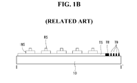
- FIG. 1B is a cross-sectional view taken along line I-I' of FIG. 1A .
- the related art touch screen panel includes a touch area A in which a touch operation is performed, a routing wiring area B in which routing wires and routing pads are formed so as to transmit and receive signals to and from the touch area A, and a pad area C.
- the touch area A includes a plurality of first touch electrode serials TS arranged in parallel in a first direction (for example, x-axis direction) on a transparent substrate 10, and a plurality of second touch electrode serials RS which are arranged in parallel in a second direction (for example, y-axis direction) on the transparent substrate 10 with an insulating layer INS interposed between the first and second touch electrode serials TS and RS and cross the first touch electrode serials TS.
- the plurality of first touch electrode serials TS and the plurality of second touch electrode serials RS cross each other and are disposed with the insulating layer INS interposed between them so that they do not contact each other.
- the routing wiring area B is formed outside the touch area A including the first and second touch electrode serials TS and RS.
- the routing wiring area B includes a plurality of first routing wires TW respectively connected to the plurality of first touch electrode serials TS and a plurality of second routing wires RW respectively connected to the plurality of second touch electrode serials RS.
- the pad area C includes a plurality of first routing pads TP respectively connected to the plurality of first routing wires TW and a plurality of second routing pads RP respectively connected to the plurality of second routing wires RW.
- FIGs. 2A to 2C Another related art touch screen panel is described below with reference to FIGs. 2A to 2C .
- FIG. 2A is a plane view of a related art touch screen panel, in which bar-shaped touch electrodes are formed on both surfaces of a transparent substrate.
- FIG. 2B is a cross-sectional view taken along line I-I' of FIG. 2A .
- FIG. 2C is a cross-sectional view taken along line II-II' of FIG. 2A .
- the related art touch screen panel includes a touch area A in which a touch operation is performed, a routing wiring area B in which routing wires and routing pads are formed so as to transmit and receive signals to and from the touch area A, and a pad area C.
- the touch area A includes a plurality of first touch electrode serials TS arranged in parallel in a first direction (for example, x-axis direction) on one surface of a transparent substrate 10, and a plurality of second touch electrode serials RS which are arranged in parallel in a second direction (for example, y-axis direction) on the other surface of the transparent substrate 10 and cross the first touch electrode serials TS.
- first direction for example, x-axis direction
- second touch electrode serials RS which are arranged in parallel in a second direction (for example, y-axis direction) on the other surface of the transparent substrate 10 and cross the first touch electrode serials TS.
- the routing wiring area B is formed outside the touch area A including the first and second touch electrode serials TS and RS.
- the routing wiring area B includes a plurality of first routing wires TW respectively connected to the plurality of first touch electrode serials TS on the one surface of the transparent substrate 10 and a plurality of second routing wires RW respectively connected to the plurality of second touch electrode serials RS on the other surface of the transparent substrate 10.
- the pad area C includes a plurality of first routing pads TP respectively connected to the plurality of first routing wires TW on the one surface of the transparent substrate 10 and a plurality of second routing pads RP respectively connected to the plurality of second routing wires RW on the other surface of the transparent substrate 10.
- the size of a bezel area is determined by widths of the first and second routing wires TW and RW formed in the routing wiring area B, a distance between the first and second routing wires TW and RW, and the sizes of the first and second routing pads TP and RP formed in the pad area C.
- the first and second routing pads TP and RP occupy only a portion of the bezel area and thus scarcely affect the size of the bezel area. Therefore, the widths of the routing wires TW and RW are substantially important to the size of the bezel area.
- the size of a bezel area is determined by widths of the first routing wires TW formed in the routing wiring area B, a distance between the first routing wires TW, and the sizes of the first routing pads TP formed in the pad area C, or widths of the second routing wires RW formed in the routing wiring area B, a distance between the second routing wires RW, and the sizes of the second routing pads RP formed in the pad area C.
- the first and second routing pads TP and RP occupy only a portion of the bezel area and thus scarcely affect the size of the bezel area. Therefore, the widths of the routing wires TW and RW are substantially important to the size of the bezel area.
- Embodiments of the invention provide a touch screen panel capable of reducing the size of a bezel area by forming first or second routing wires on not the same layer but different layers to reduce an entire area occupied by the first and second routing wires without reducing widths of the first and second routing wires.
- a touch screen panel comprising a substrate having a touch area and a routing wiring area, a plurality of first electrode serials which are formed in the touch area of the substrate and are arranged in a first direction, a plurality of second electrode serials which are formed in the touch area of the substrate and are arranged in a second direction crossing the first direction so that the plurality of second electrode serials do not contact the plurality of first electrode serials, a plurality of first routing wires which are formed in the routing wiring area of the substrate and are respectively connected to one ends of the plurality of first electrode serials, and a plurality of second routing wires which are formed in the routing wiring area of the substrate and are respectively connected to one ends of the plurality of second electrode serials, wherein odd-numbered first routing wires and even-numbered first routing wires of the plurality of first routing wires are formed on different layers.
- Odd-numbered second routing wires and even-numbered second routing wires of the plurality of second routing wires are formed on different layers.
- the touch screen panel further comprises an insulating layer formed at crossings of the plurality of first electrode serials and the plurality of second electrode serials so that the plurality of first electrode serials do not contact the plurality of second electrode serials.
- the odd-numbered first routing wires and the even-numbered first routing wires of the plurality of first routing wires are separated from each other by the insulating layer.
- the odd-numbered second routing wires and the even-numbered second routing wires of the plurality of second routing wires are separated from each other by the insulating layer.
- the plurality of first electrode serials are formed on a first surface of the substrate, and the plurality of second electrode serials are formed on a second surface opposite the first surface of the substrate.
- the odd-numbered first routing wires and the even-numbered first routing wires of the plurality of first routing wires are formed on the first surface and the second surface of the substrate.
- the odd-numbered second routing wires and the even-numbered second routing wires of the plurality of second routing wires are formed on the first surface and the second surface of the substrate.
- the odd-numbered first routing wires or the even-numbered first routing wires formed on the first surface or the second surface of the substrate are respectively connected to odd-numbered first electrode serials or even-numbered first electrode serials formed on the first surface or the second surface of the substrate through a contact hole formed in the substrate.
- the odd-numbered second routing wires or the even-numbered second routing wires formed on the first surface or the second surface of the substrate are respectively connected to odd-numbered second electrode serials or even-numbered second electrode serials formed on the first surface or the second surface of the substrate through a contact hole formed in the substrate.
- the odd-numbered routing wires and the even-numbered routing wires are formed on not the same layer but different layers, it is not necessary to secure a distance between the odd-numbered routing wires and the even-numbered routing wires so that they do not contact each other.
- the size of the routing wiring area occupied by the routing wires may decrease, and thus the size of a bezel area may decrease.
- FIG. 1A is a plane view of a related art touch screen panel, in which touch electrodes are formed on one surface of a transparent substrate;
- FIG. 1B is a cross-sectional view taken along line I-I' of FIG. 1A ;
- FIG. 2A is a plane view of a related art touch screen panel, in which bar-shaped touch electrodes are formed on both surfaces of a transparent substrate;
- FIG. 2B is a cross-sectional view taken along line I-I' of FIG. 2A ;
- FIG. 2C is a cross-sectional view taken along line II-II' of FIG. 2A ;
- FIG. 3A is a plane view of a touch screen panel according to a first embodiment of the invention.
- FIG. 3B is a cross-sectional view showing a portion R1 of FIG. 3A ;
- FIG. 3C is a cross-sectional view showing a portion R2 of FIG. 3A ;
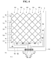
- FIG. 4 is a plane view showing a modification embodiment of the touch screen panel according to the first embodiment of the invention.
- FIG. 5 is a cross-sectional view showing an example of applying a window cover to the touch screen panel according to the first embodiment of the invention
- FIG. 6 is a cross-sectional view showing another example of applying a window cover to the touch screen panel according to the first embodiment of the invention.
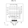
- FIG. 7A is a plane view of a touch screen panel according to a second embodiment of the invention.
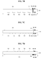
- FIGs. 7B and 7C are cross-sectional views taken along line I-I' of FIG. 7A ;
- FIG. 7D is a cross-sectional view taken along line II-II' of FIG. 7A ;
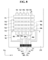
- FIG. 8 is a plane view showing a modification embodiment of the touch screen panel according to the second embodiment of the invention.
- FIG. 9 is a cross-sectional view showing an example of applying a window cover to the touch screen panel according to the second embodiment of the invention.
- FIG. 3A is a plane view of the touch screen panel according to the first embodiment of the invention.
- FIG. 3B is a cross-sectional view showing a portion R1 of FIG. 3A .
- FIG. 3C is a cross-sectional view showing a portion R2 of FIG. 3A .
- the touch screen panel according to the first embodiment of the invention includes a touch area A in which a touch operation is performed, a routing wiring area B in which routing wires used to transmit and receive a touch driving signal and a touch sensing signal are formed, and a pad area C for the connection to a touch controller.
- the touch area A includes a plurality of first touch electrode serials TS arranged in parallel in a first direction (for example, x-axis direction) on a transparent substrate 100, and a plurality of second touch electrode serials RS which are arranged in parallel in a second direction (for example, y-axis direction) on the transparent substrate 100 to cross the first touch electrode serials TS.
- An insulating layer INS is interposed between the first and second touch electrode serials TS and RS.
- Each of the first touch electrode serials TS includes a plurality of first electrode patterns Tx and a plurality of first connecting patterns Tc for connecting the adjacent first electrode patterns Tx.
- Each of the second touch electrode serials RS includes a plurality of second electrode patterns Rx and a plurality of second connecting patterns Rc for connecting the adjacent second electrode patterns Rx.
- the first connecting patterns Tc of the first touch electrode serial TS and the second connecting patterns Rc of the second touch electrode serial RS are disposed with the insulating layer INS interposed between them and cross each other, so that they do not contact each other.
- the first electrode patterns Tx of the first touch electrode serial TS are formed on the insulating layer INS, and the first connecting patterns Tc are formed on the transparent substrate 100.
- the adjacent first electrode patterns Tx are connected to each other by the first connecting pattern Tc exposed through a first contact hole CH1 formed in the insulating layer INS.
- the second electrode patterns Rx and the second connecting patterns Rc of the second touch electrode serial RS are formed on the insulating layer INS.
- FIG. 3A shows that the first and second electrode patterns Tx and Rx are formed on the insulating layer INS and the adjacent first electrode patterns Tx are connected to each other by the first connecting pattern Tc.
- the embodiment of the invention is not limited thereto.
- all of the first and second electrode patterns Tx and Rx may be formed on the transparent substrate 100, and an insulating pattern may be formed only at crossings of the first and second connecting patterns Tc and Rc so that the first and second electrode patterns Tx and Rx do not contact each other.
- FIG. 3A shows that the first and second electrode patterns Tx and Rx have a rectangle shape.
- the embodiment of the invention is not limited thereto.
- the first and second electrode patterns Tx and Rx may have various shapes including a triangle shape, a hive shape, a polygon shape, and a combination thereof.
- the routing wiring area B is formed outside the touch area A including the first and second touch electrode serials TS and RS.
- the routing wiring area B includes a plurality of first routing wires TW1 to TW5 and a plurality of second routing wires RW1 to RW5.
- the plurality of first routing wires TW1 to TW5 are alternately formed on the transparent substrate 100 and the insulating layer INS.
- the odd-numbered first routing wires TW1, TW3, and TW5 are formed on the insulating layer INS
- the even-numbered first routing wires TW2 and TW4 are formed on the transparent substrate 100.
- One ends of the odd-numbered first routing wires TW1, TW3, and TW5 formed on the insulating layer INS are respectively connected to the odd-numbered first electrode serials TS1, TS3, and TS5 on the insulating layer INS.
- One ends of the even-numbered first routing wires TW2 and TW4 formed on the transparent substrate 100 are respectively connected to the even-numbered first electrode serials TS2 and TS4 through a second contact hole CH2 of the insulating layer INS.
- the plurality of second routing wires RW1 to RW5 are alternately formed on the transparent substrate 100 and the insulating layer INS.
- the odd-numbered second routing wires RW1, RW3, and RW5 are formed on the insulating layer INS
- the even-numbered second routing wires RW2 and RW4 are formed on the transparent substrate 100.
- One ends of the odd-numbered second routing wires RW1, RW3, and RW5 formed on the insulating layer INS are respectively connected to the odd-numbered second electrode serials RS1, RS3, and RS5 on the insulating layer INS.
- One ends of the even-numbered second routing wires RW2 and RW4 formed on the transparent substrate 100 are respectively connected to the even-numbered second electrode serials RS2 and RS4 through a contact hole (not shown) of the insulating layer INS.
- the first embodiment of the invention described the touch screen panel, in which the plurality of first and second routing wires TW1 to TW5 and RW1 to RW5 are alternately formed on the transparent substrate 100 and the insulating layer INS, but is not limited thereto. It should be understood that the fact, that the plurality of first and second routing wires TW1 to TW5 and RW1 to RW5 are dividedly formed on the transparent substrate 100 and the insulating layer INS, is pertained in the scope of the embodiments of the invention.
- the pad area C is formed outside the routing wiring area B and includes a plurality of first routing pads TP1 to TP5 and a plurality of second routing pads RP1 to RP5.
- the plurality of first routing pads TP1 to TP5 are respectively connected to the other ends of the plurality of first routing wires TW1 to TW5, and the plurality of second routing pads RP1 to RP5 are respectively connected to the other ends of the plurality of second routing wires RW1 to RW5.
- the first routing wires TW1 to TW5 are alternately formed on the transparent substrate 100 and the insulating layer INS, and also the second routing wires RW1 to RW5 are alternately formed on the transparent substrate 100 and the insulating layer INS. Therefore, the odd-numbered first routing wires TW1, TW3, and TW5 and the even-numbered first routing wires TW2 and TW4 are formed on the different layers, and also the odd-numbered second routing wires RW1, RW3, and RW5 and the even-numbered second routing wires RW2 and RW4 are formed on the different layers. Hence, it is not necessary to secure a distance between the odd-numbered routing wires and the even-numbered routing wires.
- odd-numbered first routing wires and even-numbered first routing wires are formed on the same layer, and odd-numbered second routing wires and even-numbered second routing wires are formed on the same layer. Therefore, the odd-numbered routing wires and the even-numbered routing wires have to be separated from each other at a predetermined distance, so that they do not contact each other.
- the odd-numbered routing wires and the even-numbered routing wires may not contact each other because they are formed on and under the insulating layer respectively. Therefore, the size of the routing wiring area B occupied by the routing wires may decrease, and thus the size of the bezel area may decrease.
- the touch screen panel according to the first embodiment of the invention shown in FIGs. 3A to 3C described that the odd-numbered first routing wires and the odd-numbered second routing wires are formed on the insulating layer, and the even-numbered first routing wires and the even-numbered second routing wires are formed on the transparent substrate, as an example of configuration, but is not limited thereto.
- the odd-numbered first routing wires and the even-numbered second routing wires may be formed on the insulating layer, and the even-numbered first routing wires and the odd-numbered second routing wires may be formed on the transparent substrate.
- the even-numbered first routing wires and the even-numbered second routing wires may be formed on the insulating layer, and the odd-numbered first routing wires and the odd-numbered second routing wires may be formed on the transparent substrate.
- the even-numbered first routing wires and the odd-numbered second routing wires may be formed on the insulating layer, and the odd-numbered first routing wires and the even-numbered second routing wires may be formed on the transparent substrate.
- FIG. 4 is a plane view showing a modification embodiment of the touch screen panel according to the first embodiment of the invention.
- the modification embodiment shown in FIG. 4 is different from the first embodiment of the invention, in that the first routing wires TW1 to TW5 are dividedly formed on both sides of the touch area A. Thus, only a difference between the first embodiment and the modification embodiment of the invention is described below.
- some TW1 and TW2 of the first routing wires TW1 to TW5 are formed on the left side of the touch area A, and the remaining first routing wires TW3, TW4, and TW5 are formed on the right side of the touch area A.
- the odd-numbered first routing wires TW1, TW3, and TW5 and the even-numbered first routing wires TW2 and TW4 are alternately formed on the transparent substrate 100 and the insulating layer (not shown).
- the first embodiment shown in FIG. 3A and the modification embodiment shown in FIG. 4 illustrate that the first routing wires are connected only to one end of the first electrode serial, but are not limited thereto.
- the embodiments of the invention may be applied to a double routing wiring structure, in which the first routing wires are connected to both ends of the first electrode serial and signals are transmitted and received through the both ends of the first electrode serial.
- the odd-numbered first routing wires and the even-numbered second routing wires are alternately formed on the insulating layer and the transparent substrate.
- the same effect as the first embodiment of the invention may be obtained.
- FIG. 5 is a cross-sectional view showing an example of applying a window cover to the touch screen panel according to the first embodiment of the invention.
- FIG. 6 is a cross-sectional view showing another example of applying a window cover to the touch screen panel according to the first embodiment of the invention.
- the touch screen panel according to the first embodiment of the invention is attached to a window cover WC, such as a reinforced glass, using an adhesive AD and thus may be used more stably.
- a window cover WC such as a reinforced glass
- the touch screen panel uses a window cover WC, such as a reinforced glass, instead of the transparent substrate 100 shown in FIG. 3A .
- a window cover WC such as a reinforced glass
- the first and second electrode serials TS1 to TS5 and RS1 to RS5 the first and second routing wires TW1 to TW5 and RW1 to RW5, and the first and second routing pads TP1 to TP5 and RP1 to RP5 are directly formed on the window cover WC, the effect capable of protecting the touch screen panel may be obtained by the window cover WC.
- FIG. 7A is a plane view of the touch screen panel according to the second embodiment of the invention.
- FIGs. 7B and 7C are cross-sectional views taken along line I-I' of FIG. 7A .
- FIG. 7D is a cross-sectional view taken along line II-II' of FIG. 7A .
- the touch screen panel according to the second embodiment of the invention includes a touch area A in which a touch operation is performed, a routing wiring area B in which routing wires used to transmit and receive a touch driving signal and a touch sensing signal are formed, and a pad area C for the connection to a touch controller.
- the touch area A includes a plurality of first touch electrode serials TS arranged in parallel in a first direction (for example, x-axis direction) on one surface of a transparent substrate 200, and a plurality of second touch electrode serials RS which are arranged in parallel in a second direction (for example, y-axis direction) on the other surface of the transparent substrate 200 to cross the first touch electrode serials TS.
- first direction for example, x-axis direction
- second touch electrode serials RS which are arranged in parallel in a second direction (for example, y-axis direction) on the other surface of the transparent substrate 200 to cross the first touch electrode serials TS.
- FIG. 7A shows that the first and second touch electrode serials TS and RS have a bar shape.
- each of the first and second touch electrode serials TS and RS may include a plurality of electrode patterns having a triangle shape, a hive shape, a polygon shape, a circle shape, an oral shape, or a combination thereof.
- the routing wiring area B is formed outside the touch area A including the first and second touch electrode serials TS and RS.
- the routing wiring area B includes a plurality of first routing wires TW1 to TW5 and a plurality of second routing wires RW1 to RW5.
- the plurality of first routing wires TW1 to TW5 are alternately formed on one surface and the other surface of the transparent substrate 200.
- the odd-numbered first routing wires TW1, TW3, and TW5 are formed on one surface (for example, a lower surface of the transparent substrate 200 in FIGs. 7A to 7C ) of the transparent substrate 200
- the even-numbered first routing wires TW2 and TW4 are formed on the other surface (for example, an upper surface of the transparent substrate 200 in FIGs. 7A to 7C ) of the transparent substrate 200.
- One ends of the odd-numbered first routing wires TW1, TW3, and TW5 formed on the lower surface of the transparent substrate 200 are respectively connected to the odd-numbered first electrode serials TS1, TS3, and TS5 on the upper surface of the transparent substrate 200 through a contact hole CH.
- the first electrode serials TS1 to TS5 are formed on the upper surface of the transparent substrate 200, and the odd-numbered first routing wires TW1, TW3, and TW5 are formed on the lower surface of the transparent substrate 200. Therefore, the transparent substrate 200 has the contact holes CH for respectively connecting the odd-numbered first routing wires TW1, TW3, and TW5 to the odd-numbered first electrode serials TS1, TS3, and TS5.
- odd-numbered 1-1 routing wires for example, fifth 1-1 routing wires TW5a in FIG. 7B
- odd-numbered 1-2 routing wires are formed on the upper surface of the transparent substrate 200 and in the contact hole CH, so that the odd-numbered 1-2 routing wires TW5b are connected to the odd-numbered first electrode serials TS1, TS3, and TS5 and the odd-numbered 1-1 routing wires TW5a.
- odd-numbered 1-1 routing wires TW5a may be formed on the lower surface of the transparent substrate 200 and in the contact hole CH
- odd-numbered 1-2 routing wires TW5b may be formed on the upper surface of the transparent substrate 200, so that the odd-numbered 1-2 routing wires TW5b are connected to the odd-numbered first electrode serials TS1, TS3, and TS5 and the odd-numbered 1-1 routing wires TW5a.
- the odd-numbered first routing wires TW1, TW3, and TW5 may be formed only on the lower surface of the transparent substrate 200, and the odd-numbered first electrode serials TS1, TS3, and TS5 formed on the transparent substrate 200 may be respectively connected to the odd-numbered first routing wires TW1, TW3, and TW5 through the contact holes CH.
- One ends of the even-numbered first routing wires TW2 and TW4 formed on the upper surface of the transparent substrate 200 are respectively connected to the even-numbered first electrode serials TS2 and TS4 formed on the upper surface of the transparent substrate 200.
- the plurality of second routing wires RW1 to RW5 are alternately formed on one surface and the other surface of the transparent substrate 200.
- the odd-numbered second routing wires RW1, RW3, and RW5 are formed on one surface (for example, the lower surface) of the transparent substrate 200, and the even-numbered second routing wires RW2 and RW4 are formed on the other surface (for example, the upper surface) of the transparent substrate 200.
- One ends of the odd-numbered second routing wires RW1, RW3, and RW5 formed on the lower surface of the transparent substrate 200 are respectively connected to the odd-numbered second electrode serials RS1, RS3, and RS5 on the lower surface of the transparent substrate 200.
- one ends of the even-numbered second routing wires RW2 and RW4 formed on the upper surface of the transparent substrate 200 are respectively connected to the even-numbered second electrode serials RS2 and RS4 through a contact hole (not shown) formed in the transparent substrate 200.
- connection relationship between the second electrode serials RS1 to RS5 formed on the lower surface of the transparent substrate 200 and the second routing wires RW1 to RW5 is similar to a connection relationship between the first electrode serials TS1 to TS5 formed on the upper surface of the transparent substrate 200 and the first routing wires TW1 to TW5, a description of the connection relationship is omitted.
- the pad area C is formed outside the routing wiring area B and includes a plurality of first routing pads TP1 to TP5 and a plurality of second routing pads RP1 to RP5.
- the plurality of first routing pads TP1 to TP5 are respectively connected to the other ends of the plurality of first routing wires TW1 to TW5, and the plurality of second routing pads RP1 to RP5 are respectively connected to the other ends of the plurality of second routing wires RW1 to RW5.
- the first routing wires TW1 to TW5 are alternately formed on one surface (for example, the lower surface) and the other surface (for example, the upper surface) of the transparent substrate 200, and also the second routing wires RW1 to RW5 are alternately formed on one surface (for example, the lower surface) and the other surface (for example, the upper surface) of the transparent substrate 200. Therefore, the odd-numbered first routing wires TW1, TW3, and TW5 and the even-numbered first routing wires TW2 and TW4 are formed on the different layers, and also the odd-numbered second routing wires RW1, RW3, and RW5 and the even-numbered second routing wires RW2 and RW4 are formed on the different layers. Hence, it is not necessary to secure a distance between the odd-numbered routing wires and the even-numbered routing wires so that they do not contact each other.
- the odd-numbered first routing wires and the even-numbered first routing wires are formed on the same layer, and the odd-numbered second routing wires and the even-numbered second routing wires are formed on the same layer. Therefore, the odd-numbered routing wires and the even-numbered routing wires have to be separated from each other at a predetermined distance, so that they do not contact each other.
- the touch screen panel according to the second embodiment of the invention although a distance between the odd-numbered routing wires and the even-numbered routing wires is not secured, the odd-numbered routing wires and the even-numbered routing wires not contact each other because they are separated from each other. Therefore, the size of the routing wiring area B occupied by the routing wires may decrease, and thus the size of the bezel area may decrease.
- the touch screen panel according to the second embodiment of the invention shown in FIGs. 7A to 7D described that the odd-numbered first routing wires and the odd-numbered second routing wires are formed on one surface (for example, the lower surface) of the transparent substrate, and the even-numbered first routing wires and the even-numbered second routing wires are formed on the other surface (for example, the upper surface) of the transparent substrate, as an example of configuration, but is not limited thereto.
- the odd-numbered first routing wires and the even-numbered second routing wires may be formed on one surface (for example, the lower surface) of the transparent substrate, and the even-numbered first routing wires and the odd-numbered second routing wires may be formed on the other surface (for example, the upper surface) of the transparent substrate.
- the even-numbered first routing wires and the even-numbered second routing wires may be formed on one surface (for example, the lower surface) of the transparent substrate, and the odd-numbered first routing wires and the odd-numbered second routing wires may be formed on the other surface (for example, the upper surface) of the transparent substrate.
- the even-numbered first routing wires and the odd-numbered second routing wires may be formed on one surface (for example, the lower surface) of the transparent substrate, and the odd-numbered first routing wires and the even-numbered second routing wires may be formed on the other surface (for example, the upper surface) of the transparent substrate.
- FIG. 8 is a plane view showing a modification embodiment of the touch screen panel according to the second embodiment of the invention.
- the modification embodiment shown in FIG. 8 is different from the second embodiment of the invention, in that the first routing wires TW1 to TW5 are dividedly formed on both sides of the touch area A. Thus, only a difference between the second embodiment and the modification embodiment of the invention is described below.
- some TW1 and TW2 of the first routing wires TW1 to TW5 are formed on the left side of the touch area A, and the remaining first routing wires TW3, TW4, and TW5 are formed on the right side of the touch area A.
- the odd-numbered first routing wires TW1, TW3, and TW5 and the even-numbered first routing wires TW2 and TW4 are alternately formed on one surface and the other surface of a transparent substrate 200.
- the second embodiment shown in FIG. 7A and the modification embodiment shown in FIG. 8 illustrate that the first routing wires are connected only to one end of the first electrode serial, but are not limited thereto.
- the embodiments of the invention may be applied to a double routing wiring structure, in which the first routing wires are connected to both ends of the first electrode serial and signals are transmitted and received through the both ends of the first electrode serial.
- the odd-numbered first routing wires and the even-numbered second routing wires are alternately formed on one surface (for example, the lower surface) and the other surface (for example, the upper surface) of the transparent substrate.
- the same effect as the second embodiment of the invention may be obtained.
- FIG. 9 is a cross-sectional view showing an example of applying a window cover to the touch screen panel according to the second embodiment of the invention.
- the touch screen panel according to the second embodiment of the invention is attached to a window cover WC, such as a reinforced glass, using an adhesive AD and thus may be used more stably.
- a window cover WC such as a reinforced glass
- the odd-numbered routing wires and the even-numbered routing wires are formed on not the same layer but the different layers, it is not necessary to secure a distance between the odd-numbered routing wires and the even-numbered routing wires so that they do not contact each other.
- the size of the routing wiring area occupied by the routing wires may decrease, and thus the size of the bezel area may decrease.
- the routing wires may occupy about 2 mm of the bezel area of the touch screen panel.
- the adjacent routing wires are formed on the different layers. Therefore, assuming that a separation distance between the adjacent routing wires is reduced to 10 ⁇ m and the total number of channels is 51, the routing wires may occupy about 1 mm of the bezel area of the touch screen panel.
- the embodiments of the invention can reduce the bezel area to about 1/2 of the related art touch screen panel.
- first touch electrode serial is a driving electrode serial
- second touch electrode serial is a sensing electrode serial
- the number of first and second touch electrode serials, the number of first and second routing wires, and the number of first and second routing pads described in the embodiments of the invention are merely an example. The numbers may increase or decrease, if necessary or desired. Accordingly, the scope of the present invention should not be limited by the exemplary embodiments, but should be defined by the appended claims.
Landscapes
- Engineering & Computer Science (AREA)
- General Engineering & Computer Science (AREA)
- Theoretical Computer Science (AREA)
- Human Computer Interaction (AREA)
- Physics & Mathematics (AREA)
- General Physics & Mathematics (AREA)
- Position Input By Displaying (AREA)
- Structure Of Printed Boards (AREA)
Abstract
Description
- Embodiments of the invention relate to a touch screen panel, and more particularly, to a touch screen panel having a routing wire structure capable of reducing a bezel size.
- Recently, various input devices such as a keyboard, a mouse, a trackball, a joystick, and a digitizer have been used to configure an interface between users and home appliances or various kinds of information communication equipments. However, the above-described input devices cause inconveniences of learning how to use them and taking up space, thus making it difficult to improve the degree of completion of the product. Thus, demand for input devices with a simple and convenient interface and capable of reducing malfunction due to inaccurate input is growing daily. In response to this demand, a touch screen panel for enabling a user to input information by directly touching the screen with his or her hand or a pen was suggested.
- Touch screen panels are classified into a resistive type, a capacitive type, an electromagnetic type, etc. based on a method for sensing a touched portion. The resistive touch screen panel determines a touched position by a voltage gradient based on changes of resistance in a state that a DC voltage is applied to metal electrodes formed on an upper plate or a lower plate. The capacitive touch screen panel senses a touched position based on changes in capacitance generated in an upper plate or a lower plate when the user touches an equipotential conductive film formed on the upper or lower plate. The electromagnetic touch screen panel senses a touched portion by reading an LC value induced when an electronic pen touches a conductive film. In addition, an optical touch screen panel, an ultrasonic touch screen panel, etc. are known.
- In general, these types of touch screen panels include a touch area for touch recognition and a routing wiring area and a pad area which are formed outside the touch area so as to transmit and receive signals to and from touch electrodes formed in the touch area. In the disclosure, the routing wiring area and the pad area are defined as a bezel area. The size of the bezel area increases as the number of channels for connecting routing wires increases due to an increase in the size of the touch area and widths of the routing wires increase.
- A related art touch screen panel is described below with reference to
FIGs. 1A and1B . -
FIG. 1A is a plane view of a related art touch screen panel, in which touch electrodes are formed on one surface of a transparent substrate.FIG. 1B is a cross-sectional view taken along line I-I' ofFIG. 1A . - As shown in
FIGs. 1A and1B , the related art touch screen panel includes a touch area A in which a touch operation is performed, a routing wiring area B in which routing wires and routing pads are formed so as to transmit and receive signals to and from the touch area A, and a pad area C. - The touch area A includes a plurality of first touch electrode serials TS arranged in parallel in a first direction (for example, x-axis direction) on a
transparent substrate 10, and a plurality of second touch electrode serials RS which are arranged in parallel in a second direction (for example, y-axis direction) on thetransparent substrate 10 with an insulating layer INS interposed between the first and second touch electrode serials TS and RS and cross the first touch electrode serials TS. In other words, the plurality of first touch electrode serials TS and the plurality of second touch electrode serials RS cross each other and are disposed with the insulating layer INS interposed between them so that they do not contact each other. - The routing wiring area B is formed outside the touch area A including the first and second touch electrode serials TS and RS. The routing wiring area B includes a plurality of first routing wires TW respectively connected to the plurality of first touch electrode serials TS and a plurality of second routing wires RW respectively connected to the plurality of second touch electrode serials RS.
- The pad area C includes a plurality of first routing pads TP respectively connected to the plurality of first routing wires TW and a plurality of second routing pads RP respectively connected to the plurality of second routing wires RW.
- Another related art touch screen panel is described below with reference to
FIGs. 2A to 2C . -
FIG. 2A is a plane view of a related art touch screen panel, in which bar-shaped touch electrodes are formed on both surfaces of a transparent substrate.FIG. 2B is a cross-sectional view taken along line I-I' ofFIG. 2A .FIG. 2C is a cross-sectional view taken along line II-II' ofFIG. 2A . - As shown in
FIGs. 2A to 2C , the related art touch screen panel includes a touch area A in which a touch operation is performed, a routing wiring area B in which routing wires and routing pads are formed so as to transmit and receive signals to and from the touch area A, and a pad area C. - The touch area A includes a plurality of first touch electrode serials TS arranged in parallel in a first direction (for example, x-axis direction) on one surface of a
transparent substrate 10, and a plurality of second touch electrode serials RS which are arranged in parallel in a second direction (for example, y-axis direction) on the other surface of thetransparent substrate 10 and cross the first touch electrode serials TS. - The routing wiring area B is formed outside the touch area A including the first and second touch electrode serials TS and RS. The routing wiring area B includes a plurality of first routing wires TW respectively connected to the plurality of first touch electrode serials TS on the one surface of the
transparent substrate 10 and a plurality of second routing wires RW respectively connected to the plurality of second touch electrode serials RS on the other surface of thetransparent substrate 10. - The pad area C includes a plurality of first routing pads TP respectively connected to the plurality of first routing wires TW on the one surface of the
transparent substrate 10 and a plurality of second routing pads RP respectively connected to the plurality of second routing wires RW on the other surface of thetransparent substrate 10. - In the touch screen panel shown in
FIGs. 1A and1B , because the first and second routing wires TW and RW and the first and second routing pads TP and RP are formed on the same layer, the size of a bezel area is determined by widths of the first and second routing wires TW and RW formed in the routing wiring area B, a distance between the first and second routing wires TW and RW, and the sizes of the first and second routing pads TP and RP formed in the pad area C. However, the first and second routing pads TP and RP occupy only a portion of the bezel area and thus scarcely affect the size of the bezel area. Therefore, the widths of the routing wires TW and RW are substantially important to the size of the bezel area. - Further, in the touch screen panel shown in
FIGs. 2A to 2C , because the first routing wires TW and the first routing pads TP are formed on the same layer and the second routing wires RW and the second routing pads RP are formed on the same layer, the size of a bezel area is determined by widths of the first routing wires TW formed in the routing wiring area B, a distance between the first routing wires TW, and the sizes of the first routing pads TP formed in the pad area C, or widths of the second routing wires RW formed in the routing wiring area B, a distance between the second routing wires RW, and the sizes of the second routing pads RP formed in the pad area C. The first and second routing pads TP and RP occupy only a portion of the bezel area and thus scarcely affect the size of the bezel area. Therefore, the widths of the routing wires TW and RW are substantially important to the size of the bezel area. - However, when the widths of the routing wires decrease so as to reduce the size of the bezel area, resistances of the routing wires increase. Hence, a performance of the touch screen panel is reduced.
- Embodiments of the invention provide a touch screen panel capable of reducing the size of a bezel area by forming first or second routing wires on not the same layer but different layers to reduce an entire area occupied by the first and second routing wires without reducing widths of the first and second routing wires.
- In one aspect, there is a touch screen panel comprising a substrate having a touch area and a routing wiring area, a plurality of first electrode serials which are formed in the touch area of the substrate and are arranged in a first direction, a plurality of second electrode serials which are formed in the touch area of the substrate and are arranged in a second direction crossing the first direction so that the plurality of second electrode serials do not contact the plurality of first electrode serials, a plurality of first routing wires which are formed in the routing wiring area of the substrate and are respectively connected to one ends of the plurality of first electrode serials, and a plurality of second routing wires which are formed in the routing wiring area of the substrate and are respectively connected to one ends of the plurality of second electrode serials, wherein odd-numbered first routing wires and even-numbered first routing wires of the plurality of first routing wires are formed on different layers.
- Odd-numbered second routing wires and even-numbered second routing wires of the plurality of second routing wires are formed on different layers.
- The touch screen panel further comprises an insulating layer formed at crossings of the plurality of first electrode serials and the plurality of second electrode serials so that the plurality of first electrode serials do not contact the plurality of second electrode serials. The odd-numbered first routing wires and the even-numbered first routing wires of the plurality of first routing wires are separated from each other by the insulating layer.
- The odd-numbered second routing wires and the even-numbered second routing wires of the plurality of second routing wires are separated from each other by the insulating layer.
- The plurality of first electrode serials are formed on a first surface of the substrate, and the plurality of second electrode serials are formed on a second surface opposite the first surface of the substrate.
- The odd-numbered first routing wires and the even-numbered first routing wires of the plurality of first routing wires are formed on the first surface and the second surface of the substrate.
- The odd-numbered second routing wires and the even-numbered second routing wires of the plurality of second routing wires are formed on the first surface and the second surface of the substrate.
- The odd-numbered first routing wires or the even-numbered first routing wires formed on the first surface or the second surface of the substrate are respectively connected to odd-numbered first electrode serials or even-numbered first electrode serials formed on the first surface or the second surface of the substrate through a contact hole formed in the substrate.
- The odd-numbered second routing wires or the even-numbered second routing wires formed on the first surface or the second surface of the substrate are respectively connected to odd-numbered second electrode serials or even-numbered second electrode serials formed on the first surface or the second surface of the substrate through a contact hole formed in the substrate.
- In the touch screen panel according to the embodiments of the invention, because the odd-numbered routing wires and the even-numbered routing wires are formed on not the same layer but different layers, it is not necessary to secure a distance between the odd-numbered routing wires and the even-numbered routing wires so that they do not contact each other. Thus, the size of the routing wiring area occupied by the routing wires may decrease, and thus the size of a bezel area may decrease.
- The accompanying drawings, which are included to provide a further understanding of the invention and are incorporated in and constitute a part of this specification, illustrate embodiments of the invention and together with the description serve to explain the principles of the invention. In the drawings:
-
FIG. 1A is a plane view of a related art touch screen panel, in which touch electrodes are formed on one surface of a transparent substrate; -
FIG. 1B is a cross-sectional view taken along line I-I' ofFIG. 1A ; -
FIG. 2A is a plane view of a related art touch screen panel, in which bar-shaped touch electrodes are formed on both surfaces of a transparent substrate; -
FIG. 2B is a cross-sectional view taken along line I-I' ofFIG. 2A ; -
FIG. 2C is a cross-sectional view taken along line II-II' ofFIG. 2A ; -
FIG. 3A is a plane view of a touch screen panel according to a first embodiment of the invention; -
FIG. 3B is a cross-sectional view showing a portion R1 ofFIG. 3A ; -
FIG. 3C is a cross-sectional view showing a portion R2 ofFIG. 3A ; -
FIG. 4 is a plane view showing a modification embodiment of the touch screen panel according to the first embodiment of the invention; -
FIG. 5 is a cross-sectional view showing an example of applying a window cover to the touch screen panel according to the first embodiment of the invention; -
FIG. 6 is a cross-sectional view showing another example of applying a window cover to the touch screen panel according to the first embodiment of the invention; -
FIG. 7A is a plane view of a touch screen panel according to a second embodiment of the invention; -
FIGs. 7B and 7C are cross-sectional views taken along line I-I' ofFIG. 7A ; -
FIG. 7D is a cross-sectional view taken along line II-II' ofFIG. 7A ; -
FIG. 8 is a plane view showing a modification embodiment of the touch screen panel according to the second embodiment of the invention; and -
FIG. 9 is a cross-sectional view showing an example of applying a window cover to the touch screen panel according to the second embodiment of the invention. - Reference will now be made in detail to embodiments of the invention, examples of which are illustrated in the accompanying drawings. Wherever possible, the same reference numbers will be used throughout the drawings to refer to the same or like parts. It will be paid attention that detailed description of known arts will be omitted if it is determined that the arts can mislead the embodiments of the invention.
- A touch screen panel according to a first embodiment of the invention is described below with reference to
FIGs. 3A to 3C .FIG. 3A is a plane view of the touch screen panel according to the first embodiment of the invention.FIG. 3B is a cross-sectional view showing a portion R1 ofFIG. 3A .FIG. 3C is a cross-sectional view showing a portion R2 ofFIG. 3A . - As shown in
FIGs. 3A to 3C , the touch screen panel according to the first embodiment of the invention includes a touch area A in which a touch operation is performed, a routing wiring area B in which routing wires used to transmit and receive a touch driving signal and a touch sensing signal are formed, and a pad area C for the connection to a touch controller. - The touch area A includes a plurality of first touch electrode serials TS arranged in parallel in a first direction (for example, x-axis direction) on a
transparent substrate 100, and a plurality of second touch electrode serials RS which are arranged in parallel in a second direction (for example, y-axis direction) on thetransparent substrate 100 to cross the first touch electrode serials TS. An insulating layer INS is interposed between the first and second touch electrode serials TS and RS. - Each of the first touch electrode serials TS includes a plurality of first electrode patterns Tx and a plurality of first connecting patterns Tc for connecting the adjacent first electrode patterns Tx. Each of the second touch electrode serials RS includes a plurality of second electrode patterns Rx and a plurality of second connecting patterns Rc for connecting the adjacent second electrode patterns Rx. The first connecting patterns Tc of the first touch electrode serial TS and the second connecting patterns Rc of the second touch electrode serial RS are disposed with the insulating layer INS interposed between them and cross each other, so that they do not contact each other.
- The first electrode patterns Tx of the first touch electrode serial TS are formed on the insulating layer INS, and the first connecting patterns Tc are formed on the
transparent substrate 100. The adjacent first electrode patterns Tx are connected to each other by the first connecting pattern Tc exposed through a first contact hole CH1 formed in the insulating layer INS. The second electrode patterns Rx and the second connecting patterns Rc of the second touch electrode serial RS are formed on the insulating layer INS. -
FIG. 3A shows that the first and second electrode patterns Tx and Rx are formed on the insulating layer INS and the adjacent first electrode patterns Tx are connected to each other by the first connecting pattern Tc. However, the embodiment of the invention is not limited thereto. For example, all of the first and second electrode patterns Tx and Rx may be formed on thetransparent substrate 100, and an insulating pattern may be formed only at crossings of the first and second connecting patterns Tc and Rc so that the first and second electrode patterns Tx and Rx do not contact each other. - Further,
FIG. 3A shows that the first and second electrode patterns Tx and Rx have a rectangle shape. However, the embodiment of the invention is not limited thereto. For example, the first and second electrode patterns Tx and Rx may have various shapes including a triangle shape, a hive shape, a polygon shape, and a combination thereof. - The routing wiring area B is formed outside the touch area A including the first and second touch electrode serials TS and RS. The routing wiring area B includes a plurality of first routing wires TW1 to TW5 and a plurality of second routing wires RW1 to RW5.
- The plurality of first routing wires TW1 to TW5 are alternately formed on the
transparent substrate 100 and the insulating layer INS. In an example illustrated inFIGs. 3B and 3C , the odd-numbered first routing wires TW1, TW3, and TW5 are formed on the insulating layer INS, and the even-numbered first routing wires TW2 and TW4 are formed on thetransparent substrate 100. One ends of the odd-numbered first routing wires TW1, TW3, and TW5 formed on the insulating layer INS are respectively connected to the odd-numbered first electrode serials TS1, TS3, and TS5 on the insulating layer INS. One ends of the even-numbered first routing wires TW2 and TW4 formed on thetransparent substrate 100 are respectively connected to the even-numbered first electrode serials TS2 and TS4 through a second contact hole CH2 of the insulating layer INS. - In the same manner as the first routing wires TW1 to TW5, the plurality of second routing wires RW1 to RW5 are alternately formed on the
transparent substrate 100 and the insulating layer INS. In the example illustrated inFIGs. 3B and 3C , the odd-numbered second routing wires RW1, RW3, and RW5 are formed on the insulating layer INS, and the even-numbered second routing wires RW2 and RW4 are formed on thetransparent substrate 100. One ends of the odd-numbered second routing wires RW1, RW3, and RW5 formed on the insulating layer INS are respectively connected to the odd-numbered second electrode serials RS1, RS3, and RS5 on the insulating layer INS. One ends of the even-numbered second routing wires RW2 and RW4 formed on thetransparent substrate 100 are respectively connected to the even-numbered second electrode serials RS2 and RS4 through a contact hole (not shown) of the insulating layer INS. - The first embodiment of the invention described the touch screen panel, in which the plurality of first and second routing wires TW1 to TW5 and RW1 to RW5 are alternately formed on the
transparent substrate 100 and the insulating layer INS, but is not limited thereto. It should be understood that the fact, that the plurality of first and second routing wires TW1 to TW5 and RW1 to RW5 are dividedly formed on thetransparent substrate 100 and the insulating layer INS, is pertained in the scope of the embodiments of the invention. - The pad area C is formed outside the routing wiring area B and includes a plurality of first routing pads TP1 to TP5 and a plurality of second routing pads RP1 to RP5.
- The plurality of first routing pads TP1 to TP5 are respectively connected to the other ends of the plurality of first routing wires TW1 to TW5, and the plurality of second routing pads RP1 to RP5 are respectively connected to the other ends of the plurality of second routing wires RW1 to RW5.
- In the touch screen panel according to the first embodiment of the invention, the first routing wires TW1 to TW5 are alternately formed on the
transparent substrate 100 and the insulating layer INS, and also the second routing wires RW1 to RW5 are alternately formed on thetransparent substrate 100 and the insulating layer INS. Therefore, the odd-numbered first routing wires TW1, TW3, and TW5 and the even-numbered first routing wires TW2 and TW4 are formed on the different layers, and also the odd-numbered second routing wires RW1, RW3, and RW5 and the even-numbered second routing wires RW2 and RW4 are formed on the different layers. Hence, it is not necessary to secure a distance between the odd-numbered routing wires and the even-numbered routing wires. - On the other hand, in a related art touch screen panel, odd-numbered first routing wires and even-numbered first routing wires are formed on the same layer, and odd-numbered second routing wires and even-numbered second routing wires are formed on the same layer. Therefore, the odd-numbered routing wires and the even-numbered routing wires have to be separated from each other at a predetermined distance, so that they do not contact each other.
- Accordingly, in the touch screen panel according to the first embodiment of the invention, although a distance between the odd-numbered routing wires and the even-numbered routing wires is not secured, the odd-numbered routing wires and the even-numbered routing wires not contact each other because they are formed on and under the insulating layer respectively. Therefore, the size of the routing wiring area B occupied by the routing wires may decrease, and thus the size of the bezel area may decrease.
- The touch screen panel according to the first embodiment of the invention shown in
FIGs. 3A to 3C described that the odd-numbered first routing wires and the odd-numbered second routing wires are formed on the insulating layer, and the even-numbered first routing wires and the even-numbered second routing wires are formed on the transparent substrate, as an example of configuration, but is not limited thereto. For example, the odd-numbered first routing wires and the even-numbered second routing wires may be formed on the insulating layer, and the even-numbered first routing wires and the odd-numbered second routing wires may be formed on the transparent substrate. Alternatively, the even-numbered first routing wires and the even-numbered second routing wires may be formed on the insulating layer, and the odd-numbered first routing wires and the odd-numbered second routing wires may be formed on the transparent substrate. Alternatively, the even-numbered first routing wires and the odd-numbered second routing wires may be formed on the insulating layer, and the odd-numbered first routing wires and the even-numbered second routing wires may be formed on the transparent substrate. -
FIG. 4 is a plane view showing a modification embodiment of the touch screen panel according to the first embodiment of the invention. The modification embodiment shown inFIG. 4 is different from the first embodiment of the invention, in that the first routing wires TW1 to TW5 are dividedly formed on both sides of the touch area A. Thus, only a difference between the first embodiment and the modification embodiment of the invention is described below. - As shown in
FIG. 4 , some TW1 and TW2 of the first routing wires TW1 to TW5 are formed on the left side of the touch area A, and the remaining first routing wires TW3, TW4, and TW5 are formed on the right side of the touch area A. In the same manner as the first embodiment shown inFIG. 3A , the odd-numbered first routing wires TW1, TW3, and TW5 and the even-numbered first routing wires TW2 and TW4 are alternately formed on thetransparent substrate 100 and the insulating layer (not shown). - The first embodiment shown in
FIG. 3A and the modification embodiment shown inFIG. 4 illustrate that the first routing wires are connected only to one end of the first electrode serial, but are not limited thereto. For example, the embodiments of the invention may be applied to a double routing wiring structure, in which the first routing wires are connected to both ends of the first electrode serial and signals are transmitted and received through the both ends of the first electrode serial. In this instance, the odd-numbered first routing wires and the even-numbered second routing wires are alternately formed on the insulating layer and the transparent substrate. Hence, the same effect as the first embodiment of the invention may be obtained. - Examples of applying a window cover, such as a reinforced glass, to the touch screen panel according to the first embodiment and the modification embodiment of the invention are described below with reference to
FIGs. 5 and 6. FIG. 5 is a cross-sectional view showing an example of applying a window cover to the touch screen panel according to the first embodiment of the invention.FIG. 6 is a cross-sectional view showing another example of applying a window cover to the touch screen panel according to the first embodiment of the invention. - As shown in
FIG. 5 , the touch screen panel according to the first embodiment of the invention is attached to a window cover WC, such as a reinforced glass, using an adhesive AD and thus may be used more stably. As described above, an additional effect capable of protecting the touch screen panel may be obtained by attaching the window cover WC to the touch screen panel. - As shown in
FIG. 6 , the touch screen panel uses a window cover WC, such as a reinforced glass, instead of thetransparent substrate 100 shown inFIG. 3A . In this instance, because the first and second electrode serials TS1 to TS5 and RS1 to RS5, the first and second routing wires TW1 to TW5 and RW1 to RW5, and the first and second routing pads TP1 to TP5 and RP1 to RP5 are directly formed on the window cover WC, the effect capable of protecting the touch screen panel may be obtained by the window cover WC. - Next, a touch screen panel according to a second embodiment of the invention is described with reference to
FIGs. 7A to 7D .FIG. 7A is a plane view of the touch screen panel according to the second embodiment of the invention.FIGs. 7B and 7C are cross-sectional views taken along line I-I' ofFIG. 7A .FIG. 7D is a cross-sectional view taken along line II-II' ofFIG. 7A . - As shown in
FIGs. 7A to 7D , the touch screen panel according to the second embodiment of the invention includes a touch area A in which a touch operation is performed, a routing wiring area B in which routing wires used to transmit and receive a touch driving signal and a touch sensing signal are formed, and a pad area C for the connection to a touch controller. - The touch area A includes a plurality of first touch electrode serials TS arranged in parallel in a first direction (for example, x-axis direction) on one surface of a
transparent substrate 200, and a plurality of second touch electrode serials RS which are arranged in parallel in a second direction (for example, y-axis direction) on the other surface of thetransparent substrate 200 to cross the first touch electrode serials TS. -
FIG. 7A shows that the first and second touch electrode serials TS and RS have a bar shape. However, the embodiment of the invention is not limited thereto. For example, each of the first and second touch electrode serials TS and RS may include a plurality of electrode patterns having a triangle shape, a hive shape, a polygon shape, a circle shape, an oral shape, or a combination thereof. - The routing wiring area B is formed outside the touch area A including the first and second touch electrode serials TS and RS. The routing wiring area B includes a plurality of first routing wires TW1 to TW5 and a plurality of second routing wires RW1 to RW5.
- The plurality of first routing wires TW1 to TW5 are alternately formed on one surface and the other surface of the
transparent substrate 200. In an example illustrated inFIGs. 7B and 7C , the odd-numbered first routing wires TW1, TW3, and TW5 are formed on one surface (for example, a lower surface of thetransparent substrate 200 inFIGs. 7A to 7C ) of thetransparent substrate 200, and the even-numbered first routing wires TW2 and TW4 are formed on the other surface (for example, an upper surface of thetransparent substrate 200 inFIGs. 7A to 7C ) of thetransparent substrate 200. One ends of the odd-numbered first routing wires TW1, TW3, and TW5 formed on the lower surface of thetransparent substrate 200 are respectively connected to the odd-numbered first electrode serials TS1, TS3, and TS5 on the upper surface of thetransparent substrate 200 through a contact hole CH. - In the touch screen panel shown in
FIG. 7A , the first electrode serials TS1 to TS5 are formed on the upper surface of thetransparent substrate 200, and the odd-numbered first routing wires TW1, TW3, and TW5 are formed on the lower surface of thetransparent substrate 200. Therefore, thetransparent substrate 200 has the contact holes CH for respectively connecting the odd-numbered first routing wires TW1, TW3, and TW5 to the odd-numbered first electrode serials TS1, TS3, and TS5. - In this instance, as shown in
FIG. 7B , odd-numbered 1-1 routing wires (for example, fifth 1-1 routing wires TW5a inFIG. 7B ) are formed on the lower surface of thetransparent substrate 200. Further, odd-numbered 1-2 routing wires (for example, fifth 1-2 routing wires TW5b inFIG. 7B ) are formed on the upper surface of thetransparent substrate 200 and in the contact hole CH, so that the odd-numbered 1-2 routing wires TW5b are connected to the odd-numbered first electrode serials TS1, TS3, and TS5 and the odd-numbered 1-1 routing wires TW5a. - It is a matter of course that the odd-numbered 1-1 routing wires TW5a may be formed on the lower surface of the
transparent substrate 200 and in the contact hole CH, and the odd-numbered 1-2 routing wires TW5b may be formed on the upper surface of thetransparent substrate 200, so that the odd-numbered 1-2 routing wires TW5b are connected to the odd-numbered first electrode serials TS1, TS3, and TS5 and the odd-numbered 1-1 routing wires TW5a. - Alternatively, as shown in
FIG. 7C , the odd-numbered first routing wires TW1, TW3, and TW5 may be formed only on the lower surface of thetransparent substrate 200, and the odd-numbered first electrode serials TS1, TS3, and TS5 formed on thetransparent substrate 200 may be respectively connected to the odd-numbered first routing wires TW1, TW3, and TW5 through the contact holes CH. - One ends of the even-numbered first routing wires TW2 and TW4 formed on the upper surface of the
transparent substrate 200 are respectively connected to the even-numbered first electrode serials TS2 and TS4 formed on the upper surface of thetransparent substrate 200. - In the same manner as the first routing wires TW1 to TW5, the plurality of second routing wires RW1 to RW5 are alternately formed on one surface and the other surface of the
transparent substrate 200. The odd-numbered second routing wires RW1, RW3, and RW5 are formed on one surface (for example, the lower surface) of thetransparent substrate 200, and the even-numbered second routing wires RW2 and RW4 are formed on the other surface (for example, the upper surface) of thetransparent substrate 200. - One ends of the odd-numbered second routing wires RW1, RW3, and RW5 formed on the lower surface of the
transparent substrate 200 are respectively connected to the odd-numbered second electrode serials RS1, RS3, and RS5 on the lower surface of thetransparent substrate 200. Further, one ends of the even-numbered second routing wires RW2 and RW4 formed on the upper surface of thetransparent substrate 200 are respectively connected to the even-numbered second electrode serials RS2 and RS4 through a contact hole (not shown) formed in thetransparent substrate 200. Since a detailed connection relationship between the second electrode serials RS1 to RS5 formed on the lower surface of thetransparent substrate 200 and the second routing wires RW1 to RW5 is similar to a connection relationship between the first electrode serials TS1 to TS5 formed on the upper surface of thetransparent substrate 200 and the first routing wires TW1 to TW5, a description of the connection relationship is omitted. - The pad area C is formed outside the routing wiring area B and includes a plurality of first routing pads TP1 to TP5 and a plurality of second routing pads RP1 to RP5.
- The plurality of first routing pads TP1 to TP5 are respectively connected to the other ends of the plurality of first routing wires TW1 to TW5, and the plurality of second routing pads RP1 to RP5 are respectively connected to the other ends of the plurality of second routing wires RW1 to RW5.
- In the touch screen panel according to the second embodiment of the invention, the first routing wires TW1 to TW5 are alternately formed on one surface (for example, the lower surface) and the other surface (for example, the upper surface) of the
transparent substrate 200, and also the second routing wires RW1 to RW5 are alternately formed on one surface (for example, the lower surface) and the other surface (for example, the upper surface) of thetransparent substrate 200. Therefore, the odd-numbered first routing wires TW1, TW3, and TW5 and the even-numbered first routing wires TW2 and TW4 are formed on the different layers, and also the odd-numbered second routing wires RW1, RW3, and RW5 and the even-numbered second routing wires RW2 and RW4 are formed on the different layers. Hence, it is not necessary to secure a distance between the odd-numbered routing wires and the even-numbered routing wires so that they do not contact each other. - On the other hand, in the related art touch screen panel, the odd-numbered first routing wires and the even-numbered first routing wires are formed on the same layer, and the odd-numbered second routing wires and the even-numbered second routing wires are formed on the same layer. Therefore, the odd-numbered routing wires and the even-numbered routing wires have to be separated from each other at a predetermined distance, so that they do not contact each other.
- Accordingly, in the touch screen panel according to the second embodiment of the invention, although a distance between the odd-numbered routing wires and the even-numbered routing wires is not secured, the odd-numbered routing wires and the even-numbered routing wires not contact each other because they are separated from each other. Therefore, the size of the routing wiring area B occupied by the routing wires may decrease, and thus the size of the bezel area may decrease.
- The touch screen panel according to the second embodiment of the invention shown in
FIGs. 7A to 7D described that the odd-numbered first routing wires and the odd-numbered second routing wires are formed on one surface (for example, the lower surface) of the transparent substrate, and the even-numbered first routing wires and the even-numbered second routing wires are formed on the other surface (for example, the upper surface) of the transparent substrate, as an example of configuration, but is not limited thereto. - For example, the odd-numbered first routing wires and the even-numbered second routing wires may be formed on one surface (for example, the lower surface) of the transparent substrate, and the even-numbered first routing wires and the odd-numbered second routing wires may be formed on the other surface (for example, the upper surface) of the transparent substrate. Alternatively, the even-numbered first routing wires and the even-numbered second routing wires may be formed on one surface (for example, the lower surface) of the transparent substrate, and the odd-numbered first routing wires and the odd-numbered second routing wires may be formed on the other surface (for example, the upper surface) of the transparent substrate. Alternatively, the even-numbered first routing wires and the odd-numbered second routing wires may be formed on one surface (for example, the lower surface) of the transparent substrate, and the odd-numbered first routing wires and the even-numbered second routing wires may be formed on the other surface (for example, the upper surface) of the transparent substrate.
-
FIG. 8 is a plane view showing a modification embodiment of the touch screen panel according to the second embodiment of the invention. The modification embodiment shown inFIG. 8 is different from the second embodiment of the invention, in that the first routing wires TW1 to TW5 are dividedly formed on both sides of the touch area A. Thus, only a difference between the second embodiment and the modification embodiment of the invention is described below. - As shown in
FIG. 8 , some TW1 and TW2 of the first routing wires TW1 to TW5 are formed on the left side of the touch area A, and the remaining first routing wires TW3, TW4, and TW5 are formed on the right side of the touch area A. In the same manner as the second embodiment shown inFIG. 7A , the odd-numbered first routing wires TW1, TW3, and TW5 and the even-numbered first routing wires TW2 and TW4 are alternately formed on one surface and the other surface of atransparent substrate 200. - The second embodiment shown in
FIG. 7A and the modification embodiment shown inFIG. 8 illustrate that the first routing wires are connected only to one end of the first electrode serial, but are not limited thereto. For example, the embodiments of the invention may be applied to a double routing wiring structure, in which the first routing wires are connected to both ends of the first electrode serial and signals are transmitted and received through the both ends of the first electrode serial. In this instance, the odd-numbered first routing wires and the even-numbered second routing wires are alternately formed on one surface (for example, the lower surface) and the other surface (for example, the upper surface) of the transparent substrate. Hence, the same effect as the second embodiment of the invention may be obtained. - Examples of applying a window cover, such as a reinforced glass, to the touch screen panel according to the second embodiment and the modification embodiment of the invention are described below with reference to
FIG. 9. FIG. 9 is a cross-sectional view showing an example of applying a window cover to the touch screen panel according to the second embodiment of the invention. - As shown in
FIG. 9 , the touch screen panel according to the second embodiment of the invention is attached to a window cover WC, such as a reinforced glass, using an adhesive AD and thus may be used more stably. As described above, an additional effect capable of protecting the touch screen panel may be obtained by attaching the window cover WC to the touch screen panel. - As described above, in the touch screen panel according to the embodiments of the invention, because the odd-numbered routing wires and the even-numbered routing wires are formed on not the same layer but the different layers, it is not necessary to secure a distance between the odd-numbered routing wires and the even-numbered routing wires so that they do not contact each other. Thus, the size of the routing wiring area occupied by the routing wires may decrease, and thus the size of the bezel area may decrease.
- For example, in the related art touch screen panel, assuming that a width of the routing wire is 10 µm, a proper separation distance between the adjacent routing wires is 30 µm, and the total number of channels is 51, the routing wires may occupy about 2 mm of the bezel area of the touch screen panel. On the other hand, in the touch screen panel according to the embodiments of the invention, the adjacent routing wires are formed on the different layers. Therefore, assuming that a separation distance between the adjacent routing wires is reduced to 10 µm and the total number of channels is 51, the routing wires may occupy about 1 mm of the bezel area of the touch screen panel. Hence, the embodiments of the invention can reduce the bezel area to about 1/2 of the related art touch screen panel.
- Although embodiments have been described with reference to a number of illustrative embodiments thereof, it should be understood that numerous other modifications and embodiments can be devised by those skilled in the related art. For example, the embodiments of the invention described that the first touch electrode serial is a driving electrode serial and the second touch electrode serial is a sensing electrode serial, but the reverse case is possible. Further, it should be understood that the number of first and second touch electrode serials, the number of first and second routing wires, and the number of first and second routing pads described in the embodiments of the invention are merely an example. The numbers may increase or decrease, if necessary or desired. Accordingly, the scope of the present invention should not be limited by the exemplary embodiments, but should be defined by the appended claims.
Claims (9)
- A touch screen panel comprising:a substrate having a touch area and a routing wiring area;a plurality of first electrode serials which are formed in the touch area of the substrate and are arranged in a first direction;a plurality of second electrode serials which are formed in the touch area of the substrate and are arranged in a second direction crossing the first direction so that the plurality of second electrode serials do not contact the plurality of first electrode serials;a plurality of first routing wires which are formed in the routing wiring area of the substrate and are respectively connected to one ends of the plurality of first electrode serials; anda plurality of second routing wires which are formed in the routing wiring area of the substrate and are respectively connected to one ends of the plurality of second electrode serials,wherein odd-numbered first routing wires and even-numbered first routing wires of the plurality of first routing wires are formed on different layers.
- The touch screen panel of claim 1, wherein odd-numbered second routing wires and even-numbered second routing wires of the plurality of second routing wires are formed on different layers.
- The touch screen panel of claim 1 or 2, further comprising an insulating layer formed at crossings of the plurality of first electrode serials and the plurality of second electrode serials so that the plurality of first electrode serials do not contact the plurality of second electrode serials,
wherein the odd-numbered first routing wires and the even-numbered first routing wires of the plurality of first routing wires are separated from each other by the insulating layer. - The touch screen panel of claim 3, wherein odd-numbered second routing wires and even-numbered second routing wires of the plurality of second routing wires are separated from each other by the insulating layer.
- The touch screen panel of claim 1, wherein the plurality of first electrode serials are formed on a first surface of the substrate,
wherein the plurality of second electrode serials are formed on a second surface opposite the first surface of the substrate. - The touch screen panel of claim 5, wherein the odd-numbered first routing wires and the even-numbered first routing wires of the plurality of first routing wires are formed on the first surface and the second surface of the substrate.
- The touch screen panel of claim 5 or 6, wherein odd-numbered second routing wires and even-numbered second routing wires of the plurality of second routing wires are formed on the first surface and the second surface of the substrate.
- The touch screen panel of claim 7, wherein the odd-numbered first routing wires or the even-numbered first routing wires formed on the first surface or the second surface of the substrate are respectively connected to odd-numbered first electrode serials or even-numbered first electrode serials formed on the first surface or the second surface of the substrate through a contact hole formed in the substrate.
- The touch screen panel of claim 7, wherein the odd-numbered second routing wires or the even-numbered second routing wires formed on the first surface or the second surface of the substrate are respectively connected to odd-numbered second electrode serials or even-numbered second electrode serials formed on the first surface or the second surface of the substrate through a contact hole formed in the substrate.
Applications Claiming Priority (1)
| Application Number | Priority Date | Filing Date | Title |
|---|---|---|---|
| KR1020120116811A KR101981531B1 (en) | 2012-10-19 | 2012-10-19 | Touch screen panel |
Publications (2)
| Publication Number | Publication Date |
|---|---|
| EP2722740A2 true EP2722740A2 (en) | 2014-04-23 |
| EP2722740A3 EP2722740A3 (en) | 2015-02-25 |
Family
ID=49322197
Family Applications (1)
| Application Number | Title | Priority Date | Filing Date |
|---|---|---|---|
| EP13186937.2A Withdrawn EP2722740A3 (en) | 2012-10-19 | 2013-10-01 | Touch screen panel |
Country Status (4)
| Country | Link |
|---|---|
| US (1) | US9240297B2 (en) |
| EP (1) | EP2722740A3 (en) |
| KR (1) | KR101981531B1 (en) |
| CN (1) | CN103777809B (en) |
Families Citing this family (13)
| Publication number | Priority date | Publication date | Assignee | Title |
|---|---|---|---|---|
| DE102013104644B4 (en) * | 2013-05-06 | 2020-06-04 | Polylc Gmbh & Co. Kg | Layer electrode for touch screens |
| KR102355326B1 (en) * | 2014-07-24 | 2022-01-26 | 삼성디스플레이 주식회사 | Touch screen panel and fabrication method of the same |
| KR102387980B1 (en) * | 2015-04-14 | 2022-04-18 | 삼성디스플레이 주식회사 | Touch panel and display device |
| CN106201106B (en) * | 2016-07-29 | 2019-03-19 | 上海天马微电子有限公司 | Touch display panel |
| CN106873835B (en) * | 2017-02-23 | 2020-05-05 | 武汉华星光电技术有限公司 | Touch panel, manufacturing method thereof and touch display screen |
| JP2018147348A (en) * | 2017-03-08 | 2018-09-20 | 株式会社ジャパンディスプレイ | Display device |
| US10656761B2 (en) * | 2017-04-26 | 2020-05-19 | Dell Products L.P. | Touch screen and method of compensating for differences in routing trace path lengths |
| KR102377527B1 (en) * | 2017-09-01 | 2022-03-24 | 삼성디스플레이 주식회사 | Input sensing unit and display device having the same |
| CN109917957B (en) * | 2019-02-27 | 2023-11-21 | 上海天马微电子有限公司 | Touch panel, manufacturing method and repairing method thereof and touch device |
| KR102830839B1 (en) * | 2019-12-30 | 2025-07-04 | 엘지디스플레이 주식회사 | Touch Film And Method Of Fabricating Touch Display Device Using The Same |
| CN113129770A (en) * | 2020-01-16 | 2021-07-16 | 重庆康佳光电技术研究院有限公司 | Display back plate, display equipment and splicing display equipment |
| KR102909136B1 (en) * | 2020-05-14 | 2026-01-09 | 삼성디스플레이 주식회사 | Touch sensor and display device including the same |
| CN113835566A (en) * | 2021-09-27 | 2021-12-24 | Tcl华星光电技术有限公司 | Substrate and display panel |
Citations (1)
| Publication number | Priority date | Publication date | Assignee | Title |
|---|---|---|---|---|
| WO2012015177A2 (en) * | 2010-07-30 | 2012-02-02 | 일진디스플레이(주) | Electrode line structure and capacitive touch sensor using same |
Family Cites Families (12)
| Publication number | Priority date | Publication date | Assignee | Title |
|---|---|---|---|---|
| CN1301426C (en) * | 2003-08-19 | 2007-02-21 | 友达光电股份有限公司 | Liquid crystal display panel with narrow frame design and manufacturing method thereof |
| KR100898221B1 (en) * | 2007-04-30 | 2009-05-18 | 안영수 | Capacitive touch screen and manufacturing method |
| US8400408B2 (en) * | 2007-06-13 | 2013-03-19 | Apple Inc. | Touch screens with transparent conductive material resistors |
| US7538288B1 (en) * | 2008-03-31 | 2009-05-26 | Mildex Optical Inc. | Touch panel |
| JP5036865B2 (en) * | 2008-05-16 | 2012-09-26 | シャープ株式会社 | Active matrix substrate, display device, active matrix substrate inspection method, and display device inspection method |
| CN101639594A (en) * | 2008-08-01 | 2010-02-03 | 群康科技(深圳)有限公司 | Liquid crystal display device |
| JP5084698B2 (en) * | 2008-10-29 | 2012-11-28 | 京セラ株式会社 | Touch panel and touch panel display device |
| WO2010075308A2 (en) * | 2008-12-26 | 2010-07-01 | Atmel Corporation | Multiple electrode touch sensitive device |
| KR101093326B1 (en) * | 2010-02-18 | 2011-12-14 | 삼성모바일디스플레이주식회사 | Touch screen panel and its manufacturing method |
| CN201788340U (en) * | 2010-05-26 | 2011-04-06 | 福州华映视讯有限公司 | Active component array substrate |
| CN102279688A (en) * | 2010-06-12 | 2011-12-14 | 深圳欧菲光科技股份有限公司 | Conducting circuits for resistance type touch screen with multi-point touch control |
| KR101719368B1 (en) * | 2010-07-14 | 2017-03-24 | 엘지디스플레이 주식회사 | Electrostatic capacity type touch screen panel and method of manufacturing the same |
-
2012
- 2012-10-19 KR KR1020120116811A patent/KR101981531B1/en active Active
-
2013
- 2013-10-01 EP EP13186937.2A patent/EP2722740A3/en not_active Withdrawn
- 2013-10-09 US US14/049,586 patent/US9240297B2/en active Active
- 2013-10-11 CN CN201310473376.XA patent/CN103777809B/en not_active Expired - Fee Related
Patent Citations (1)
| Publication number | Priority date | Publication date | Assignee | Title |
|---|---|---|---|---|
| WO2012015177A2 (en) * | 2010-07-30 | 2012-02-02 | 일진디스플레이(주) | Electrode line structure and capacitive touch sensor using same |
Also Published As
| Publication number | Publication date |
|---|---|
| KR101981531B1 (en) | 2019-05-23 |
| US9240297B2 (en) | 2016-01-19 |
| EP2722740A3 (en) | 2015-02-25 |
| US20140110236A1 (en) | 2014-04-24 |
| CN103777809B (en) | 2017-07-04 |
| KR20140050418A (en) | 2014-04-29 |
| CN103777809A (en) | 2014-05-07 |
Similar Documents
| Publication | Publication Date | Title |
|---|---|---|
| US9240297B2 (en) | Touch screen panel | |
| KR102247135B1 (en) | Electrostatic capacitive type touch-sensitive panel for display device | |
| CN103777810B (en) | Metal mesh type touch screen panel | |
| CN104423760B (en) | For the capacitance type contact type panel of display device | |
| US8614680B2 (en) | Touch substrate and touch display panel | |
| JP5591834B2 (en) | Touch panel sensor | |
| KR102043847B1 (en) | Electrostatic capacitive type touch screen panel | |
| JP5684728B2 (en) | Input device | |
| TWI426427B (en) | Touch panel | |
| US20140293163A1 (en) | Touch panel | |
| JP6630433B2 (en) | Input device | |
| US9395854B2 (en) | Touch sensing panel | |
| CN101925872A (en) | Touch sensor board with split electrode structure and touch sensor device provided with the electrode structure | |
| CN103135831B (en) | touch panel | |
| KR20140063315A (en) | Mutual capacitance type touch sreen panel | |
| KR20150009420A (en) | Touch window | |
| CN112654954A (en) | Touch panel, manufacturing method thereof and electronic device | |
| US20140210768A1 (en) | Single Layer Touch Sensor | |
| KR20130019105A (en) | Touch screen panel for display device | |
| CN108874222A (en) | Touch substrate, touch screen and touch device | |
| KR102262553B1 (en) | Touch panel | |
| KR20140037528A (en) | Display device including mesh type touch sensor | |
| KR20150066860A (en) | Touch sensor integrated type flat panel display | |
| KR20130003215A (en) | Touch screen panel for display device | |
| KR102052745B1 (en) | Display Device with Thin Film Touch Sensor |
Legal Events
| Date | Code | Title | Description |
|---|---|---|---|
| PUAI | Public reference made under article 153(3) epc to a published international application that has entered the european phase |
Free format text: ORIGINAL CODE: 0009012 |
|
| AK | Designated contracting states |
Kind code of ref document: A2 Designated state(s): AL AT BE BG CH CY CZ DE DK EE ES FI FR GB GR HR HU IE IS IT LI LT LU LV MC MK MT NL NO PL PT RO RS SE SI SK SM TR |
|
| AX | Request for extension of the european patent |
Extension state: BA ME |
|
| 17P | Request for examination filed |
Effective date: 20140327 |
|
| RBV | Designated contracting states (corrected) |
Designated state(s): AL AT BE BG CH CY CZ DE DK EE ES FI FR GB GR HR HU IE IS IT LI LT LU LV MC MK MT NL NO PL PT RO RS SE SI SK SM TR |
|
| PUAL | Search report despatched |
Free format text: ORIGINAL CODE: 0009013 |
|
| RIC1 | Information provided on ipc code assigned before grant |
Ipc: G06F 3/041 20060101ALI20150115BHEP Ipc: G06F 3/044 20060101AFI20150115BHEP |
|
| AK | Designated contracting states |
Kind code of ref document: A3 Designated state(s): AL AT BE BG CH CY CZ DE DK EE ES FI FR GB GR HR HU IE IS IT LI LT LU LV MC MK MT NL NO PL PT RO RS SE SI SK SM TR |
|
| AX | Request for extension of the european patent |
Extension state: BA ME |
|
| 17Q | First examination report despatched |
Effective date: 20160114 |
|
| STAA | Information on the status of an ep patent application or granted ep patent |
Free format text: STATUS: THE APPLICATION IS DEEMED TO BE WITHDRAWN |
|
| 18D | Application deemed to be withdrawn |
Effective date: 20160525 |