EP2722639A1 - Method for measuring layer thickness of multilayer ceramic - Google Patents
Method for measuring layer thickness of multilayer ceramic Download PDFInfo
- Publication number
- EP2722639A1 EP2722639A1 EP13188420.7A EP13188420A EP2722639A1 EP 2722639 A1 EP2722639 A1 EP 2722639A1 EP 13188420 A EP13188420 A EP 13188420A EP 2722639 A1 EP2722639 A1 EP 2722639A1
- Authority
- EP
- European Patent Office
- Prior art keywords
- layer
- terahertz wave
- layer thickness
- peak
- ceramic
- Prior art date
- Legal status (The legal status is an assumption and is not a legal conclusion. Google has not performed a legal analysis and makes no representation as to the accuracy of the status listed.)
- Withdrawn
Links
- 239000000919 ceramic Substances 0.000 title claims abstract description 74
- 238000000034 method Methods 0.000 title claims abstract description 53
- 230000001678 irradiating effect Effects 0.000 claims abstract description 5
- 229910010293 ceramic material Inorganic materials 0.000 claims description 4
- 239000010410 layer Substances 0.000 description 164
- 239000000523 sample Substances 0.000 description 66
- 230000003287 optical effect Effects 0.000 description 45
- 229910001233 yttria-stabilized zirconia Inorganic materials 0.000 description 44
- 238000005259 measurement Methods 0.000 description 24
- 238000001514 detection method Methods 0.000 description 17
- 239000000758 substrate Substances 0.000 description 8
- 239000011247 coating layer Substances 0.000 description 7
- 230000005684 electric field Effects 0.000 description 7
- 230000002349 favourable effect Effects 0.000 description 7
- 238000010276 construction Methods 0.000 description 6
- 239000013078 crystal Substances 0.000 description 6
- 239000000835 fiber Substances 0.000 description 6
- 239000000463 material Substances 0.000 description 6
- 238000007689 inspection Methods 0.000 description 4
- 238000010030 laminating Methods 0.000 description 4
- 230000000704 physical effect Effects 0.000 description 4
- 230000001360 synchronised effect Effects 0.000 description 4
- 229910001218 Gallium arsenide Inorganic materials 0.000 description 3
- 230000001934 delay Effects 0.000 description 3
- 238000010586 diagram Methods 0.000 description 3
- 238000001914 filtration Methods 0.000 description 3
- 238000005086 pumping Methods 0.000 description 3
- 238000006243 chemical reaction Methods 0.000 description 2
- 239000011248 coating agent Substances 0.000 description 2
- 238000000576 coating method Methods 0.000 description 2
- 239000000284 extract Substances 0.000 description 2
- 230000006870 function Effects 0.000 description 2
- 238000003475 lamination Methods 0.000 description 2
- 229910052751 metal Inorganic materials 0.000 description 2
- 239000002184 metal Substances 0.000 description 2
- 239000004065 semiconductor Substances 0.000 description 2
- 239000000126 substance Substances 0.000 description 2
- 229910052691 Erbium Inorganic materials 0.000 description 1
- -1 GnSe Inorganic materials 0.000 description 1
- 229910003334 KNbO3 Inorganic materials 0.000 description 1
- 229910003327 LiNbO3 Inorganic materials 0.000 description 1
- 229910012463 LiTaO3 Inorganic materials 0.000 description 1
- 229910010252 TiO3 Inorganic materials 0.000 description 1
- QCWXUUIWCKQGHC-UHFFFAOYSA-N Zirconium Chemical compound [Zr] QCWXUUIWCKQGHC-UHFFFAOYSA-N 0.000 description 1
- 229910007709 ZnTe Inorganic materials 0.000 description 1
- 239000000654 additive Substances 0.000 description 1
- 230000002238 attenuated effect Effects 0.000 description 1
- 229910002113 barium titanate Inorganic materials 0.000 description 1
- 238000004364 calculation method Methods 0.000 description 1
- 230000006378 damage Effects 0.000 description 1
- 230000007423 decrease Effects 0.000 description 1
- 230000003111 delayed effect Effects 0.000 description 1
- 238000005516 engineering process Methods 0.000 description 1
- UYAHIZSMUZPPFV-UHFFFAOYSA-N erbium Chemical compound [Er] UYAHIZSMUZPPFV-UHFFFAOYSA-N 0.000 description 1
- 230000005284 excitation Effects 0.000 description 1
- 238000002474 experimental method Methods 0.000 description 1
- 239000011521 glass Substances 0.000 description 1
- 238000010438 heat treatment Methods 0.000 description 1
- 230000001771 impaired effect Effects 0.000 description 1
- 230000008676 import Effects 0.000 description 1
- 238000005304 joining Methods 0.000 description 1
- 239000004973 liquid crystal related substance Substances 0.000 description 1
- 238000004519 manufacturing process Methods 0.000 description 1
- 239000013307 optical fiber Substances 0.000 description 1
- 230000010355 oscillation Effects 0.000 description 1
- 230000003534 oscillatory effect Effects 0.000 description 1
- 239000003973 paint Substances 0.000 description 1
- 239000011347 resin Substances 0.000 description 1
- 229920005989 resin Polymers 0.000 description 1
- 230000004044 response Effects 0.000 description 1
- 238000005070 sampling Methods 0.000 description 1
- 238000007789 sealing Methods 0.000 description 1
- 238000004088 simulation Methods 0.000 description 1
- 230000002123 temporal effect Effects 0.000 description 1
- JOXIMZWYDAKGHI-UHFFFAOYSA-N toluene-4-sulfonic acid Chemical compound CC1=CC=C(S(O)(=O)=O)C=C1 JOXIMZWYDAKGHI-UHFFFAOYSA-N 0.000 description 1
- 229910052726 zirconium Inorganic materials 0.000 description 1
Images




Classifications
-
- G—PHYSICS
- G01—MEASURING; TESTING
- G01B—MEASURING LENGTH, THICKNESS OR SIMILAR LINEAR DIMENSIONS; MEASURING ANGLES; MEASURING AREAS; MEASURING IRREGULARITIES OF SURFACES OR CONTOURS
- G01B11/00—Measuring arrangements characterised by the use of optical techniques
- G01B11/02—Measuring arrangements characterised by the use of optical techniques for measuring length, width or thickness
- G01B11/06—Measuring arrangements characterised by the use of optical techniques for measuring length, width or thickness for measuring thickness ; e.g. of sheet material
- G01B11/0616—Measuring arrangements characterised by the use of optical techniques for measuring length, width or thickness for measuring thickness ; e.g. of sheet material of coating
- G01B11/0625—Measuring arrangements characterised by the use of optical techniques for measuring length, width or thickness for measuring thickness ; e.g. of sheet material of coating with measurement of absorption or reflection
Definitions
- This disclosure relates to a method for measuring thickness of each layer included in multilayer ceramic.
- a multilayer ceramic formed by laminating plural ceramic layers is applied as electronic components, for example, condensers and substrates.
- the multilayer ceramic is formed by pressure bonding (joining) or heating the laminated, or stacked ceramic layers.
- a thickness of each layer is measurable on the basis of the physical properties different from one another.
- the multilayer ceramic which is formed by laminating plural ceramic layers each being made from the same material and having various porosities, because the physical properties of each layer are similar, it is difficult to measure the thickness by means of the known method which depends on physical properties of ceramic layers. In those circumstances, a region which has porosities within a predetermined range at the multilayer ceramic in which porosities vary in a thickness direction and which is made from the same material is defined as a layer.
- each layer of the multilayer ceramic i.e., the thickness of the region which includes the porosities within the predetermined range set at each layer
- an applicable method for measuring a layer thickness of multilayer ceramic is needed.
- Patent reference 1 JP2004-333366A (i.e., hereinafter referred to as Patent reference 1) discloses a method for measuring layer thickness of the multilayer ceramic without destructing layers of the multilayer ceramic (nondestructive measurement) using ultrasonic waves.
- a thickness of each layer of multilayer ceramic may be measured by the observation using, for example, an electron microscope.
- this method is disadvantageous in terms of time consumption and manufacturing cost. Further, in this method, products to be marketed cannot be evaluated.
- the disclosure provides a method for measuring a layer thickness, which includes a process for generating a terahertz wave, a process for irradiating the terahertz wave to a multilayer ceramic having a plurality of ceramic layers, a process for obtaining a time waveform of the terahertz wave reflected on the multilayer ceramic, and a process for measuring a layer thickness of the ceramic layer on the basis of the time waveform.
- a layer thickness of each of the layers included in the multilayer ceramic is measurable in a non-contact and nondestructive manner.
- the multilayer ceramic includes a first ceramic layer, and a second ceramic layer which is in contact with the first ceramic layer and includes a porosity different from a porosity of the first ceramic layer.
- the first ceramic layer and the second ceramic layer are formed using a same ceramic material.
- the process for measuring the layer thickness includes a process for detecting two peaks corresponding to interfaces of the ceramic layers in the time waveform and a process for calculating the layer thickness on the basis of a time difference between said two peaks.
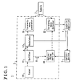
- Fig. 1 is a block diagram of an inspection system for inspecting multilayer ceramic according to an embodiment disclosed here;
- Fig. 2 is a schematic view of an optical system according to the embodiment disclosed here;
- Fig. 3 is a block diagram of a control device according to the embodiment disclosed here;
- Fig. 4 is a cross-sectional view of a sample including multilayer ceramic according to the embodiment disclosed here;
- Fig. 5 shows an example of peak patterns according to the embodiment disclosed here
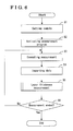
- Fig. 6 shows a flowchart for a method for measuring a layer thickness of multilayer ceramic according to the embodiment disclosed here;
- Fig. 7 shows a flowchart for a layer thickness measurement process according to the embodiment disclosed here
- Fig. 8A shows a flowchart for a peak detection processing according to the embodiment disclosed here;
- Fig. 8B shows the flowchart for the peak detection processing according to the embodiment disclosed here;
- Fig. 9 shows a waveform data of a terahertz wave according to the embodiment disclosed here.
- Fig. 10 shows a layer thickness measurement result according to the embodiment disclosed here.
- Fig. 1 shows a block diagram of an inspection system 1 for multilayer ceramic according to the embodiment.
- a broken line shows an optical path which laser beams or terahertz waves pass through and a solid line shows a physical connection.
- Directions of light and electric signals are indicated with arrows.
- the inspection system 1 includes an optical system 2 irradiating the terahertz wave to a sample 3 which includes the multilayer ceramic and detecting a reflective wave, a lock-in amplifier 4 synchronously amplifying detection signal of the reflective wave, and a control device 5 for controlling the optical system 2.
- the optical system 2 includes a laser 10, a splitter 11, a modulator 12, a terahertz wave generator 15, a terahertz wave detector 22, and an optical delay portion 25.
- the laser beam irradiated from the laser 10 is split by the splitter 11 into a fundamental wave A and a second harmonic B.
- the fundamental wave A is modulated into a pulse with a predetermined frequency by means of the modulator 12 to be incident on the terahertz wave generator 15 as a pumping light.
- the terahertz wave generated at the terahertz wave generator 15 is irradiated to the sample 3, and the reflective wave which is the terahertz wave reflected on the surface of the sample 3 assumes to be incident on, or enters the terahertz wave detector 22.
- the second harmonic B obtained by splitting the laser beam by the splitter 11 is applied as a probe light.
- the probe light is delayed by the optical delay portion 25 to be incident onto the terahertz wave detector 22.
- the terahertz wave detector 22 detects the reflective wave from the sample 3 at a timing when the probe light reaches.
- the lock-in amplifier 4 is configured to amplify signals with high signal-to-noise ratio by detecting and integrating detected electric current while being synchronized with modulation frequency.
- the signal amplified by the lock-in amplifier 4 is inputted into the control device 5 as measurement data.
- the control device 5 controls the optical delay portion 25 for varying delays of probe light (i.e., changing timings that the probe light reaches) and detects the reflective wave via the lock-in amplifier 4 to acquire a time waveform. Then, the control device 5 analyzes the time waveform of the reflective wave and calculates the layer thickness of the multilayer ceramic.
- the optical system 2 includes a femtosecond fiber laser 10, a dichroic mirror (splitter) 11, a chopper (modulator) 12, a mirror 13, a fundamental wave collecting parabolic mirror 14, a DAST (terahertz wave generator) 15, an off-axis parabolic mirrors 16, 17, 18, 20, an aperture 19, a terahertz wave detector 22, a condenser lens 23, an optical delay portion 25, and a mirror 26.
- the optical system 2 is sealed from the outside by means of a case. It is favorable that the inside of the case is dehumidified, the gas is charged into the case, or the inside of the case is vacuumed. According to the foregoing construction, it is prevented that the terahertz wave is absorbed by moisture in the air.
- the femtosecond fiber laser 10 is configured to generate the light at 1550nm wavelength by exciting an optical fiber doped with, for example, erbium (Er) by means of the excitation light.
- the generated light at 1550nm wavelength is resonated between a pair of mirrors, and outputted as a high-power light pulse via a polarized beam splitter.
- the outputted light pulse includes the fundamental wave corresponding to 1550nm component and the second harmonic corresponding to 780nm component.
- 1 micron band, or 1.5 micron band serves as the fundamental wave. It is favorable to generate the second harmonic serving as the probe light in a case where a dipole antenna with GaAs substrate is applied as the terahertz wave detector 22.
- the dichroic mirror 11 is structured by coating a white board glass with dielectric substances having different refractive indexes alternatively and splits the light pulse outputted from the femtosecond fiber laser 10 into the fundamental wave A corresponding to 1550nm component and the second harmonic B corresponding to 780nm component.
- the intensity of the fundamental wave A corresponding to 1550nm component is approximately 100mW, and a pulse width of the fundamental wave A is 17fs.
- the intensity of the second harmonic B corresponding to 780nm component is approximately 10mW, and a pulse width of the second harmonic B is 37fs.
- the fundamental wave A with 1550nm wavelength is used for generating a terahertz wave
- the second harmonic B with 780nm wavelength is used as a probe light at the terahertz wave detector.
- the wavelengths are not limited to the foregoing examples, and other numerical values, or wavelengths are applicable.
- a beam splitter for a fundamental wave may be applied and a wavelength conversion element may be positioned between the beam splitter and the optical delay portion 25.
- the wavelength bandwidth of the beam splitter is as broad as possible.
- a thickness of an element of the beam splitter is assumed to be equal to or smaller than 0.5mm.
- the fundamental wave may be split by the beam splitter.
- the chopper 12 is provided at an optical path of the fundamental wave A which transmits, or passes through the dichroic mirror 11.
- the chopper 12 may be replaced by an acosto-optic element (Acousto-Optic Modulator, AOM) or an electro-optic element (Electro-Optic Modulator, EOM).
- AOM Acoustic-Optic Modulator
- EOM Electro-Optic Modulator
- the modulation frequency by the chopper 12 is set at a relatively high level, for example, about one-tenth of repetition frequency of the laser (i.e., pulse repetition frequency), and the modulation frequency at 1 kHz is applied according to the embodiment.
- the chopper 12 is configured to output signals of the modulation frequency, and the modulation frequency is inputted to the lock-in amplifier 4. According to the foregoing construction, the lock-in amplifier 4 is allowed to perform detection synchronous to the modulation frequency.
- the mirror 13 directs the optical path of the fundamental wave modulated by the chopper 12 towards the fundamental wave collecting parabolic mirror 14.
- the fundamental wave collecting parabolic mirror 14 is arranged to collect, or to condense the fundamental wave reflected at the mirror 13 to the DAST 15.
- the DAST (4-dimethylamino-N- methyl-4-stilbazolium tosylate) 15 is an organic nonlinear optical crystal known as an organic nonlinear optical crystal having high optical constant.
- a femtosecond fiber laser which is an ultra short pulse laser, a terahertz wave equal to or greater than a few ten THz can be generated.
- the application is not limited to the DAST.
- a laser wavelength conversion nonlinear crystal for example, LiNbO 3 , MgO doped LiTaO 3 , BBO, LBO, KTP, and a semiconductor crystal, for example, ZnTe, GnSe, GaP, GaAs may be applicable.
- KDP, ADP, KNbO 3 , BaTiO 3 , and lead system or zirconium system ferrodielectric crystal may be applicable.
- lead system relaxor for example, PMN, PZN, PZT, and a quantum paraelectric system relaxor substance, for example, KT a1-x NbxO 3 , K 1-x Li x TaO 3 , Sr 1-x Ca x TiO 3 (0 ⁇ x ⁇ 1) may be applicable.
- a wave transmitting type or wave reflective type terahertz wave generating antenna may be applicable.
- the terahertz wave generated by the DAST 15 is reflected and collected at the off-axis parabolic mirrors 16, 17 to be radiated to the sample 3.
- the terahertz wave reflected at the sample 3 is reflected and collected at the off-axis parabolic mirrors 18, 20 to be incident to the terahertz wave detector 22.
- a window 2A is provided at a case which covers the optical system 2, the terahertz wave passes through the window 2A to be irradiated to the sample 3, and the terahertz wave reflected at the sample 3 passes through the window 2A to be incident on, or to enter the optical system 2.
- the window 2A is closed by a transparent member at least for the terahertz wave (i.e., a member transmitting at least terahertz wave) so that the sealing performance of the case for the optical system 2 is not impaired.
- a transparent member at least for the terahertz wave i.e., a member transmitting at least terahertz wave
- the off-axis parabolic mirrors 18, 20 collect the terahertz reflected at the sample 3 to the terahertz wave detector 22.
- the aperture 19 is provided between the off-axis parabolic mirrors 18, 20. Because a minute, or hyper fine protrusions and recesses exist on the sample 3, differences in length of path is generated between a reflective wave at a center portion of the terahertz wave (i.e., referred to as a regular reflection wave) and a reflective wave at a periphery portion of the terahertz wave. In consequence, detection resolution of the layer thickness may decline.
- the aperture 19 is adjusted to block the reflective wave at the periphery portion of the terahertz wave and to allow the regular reflection wave to enter, or to be incident on the terahertz wave detector 22.
- the aperture 19 may be provided between the sample 3 and the off-axis parabolic mirror 18. Further, alternatively, the plural apertures 19 may be provided on an optical path of the reflective wave.
- the terahertz wave detector 22 is formed as a dipole antenna by providing a metal electrode having a gap on a substrate made from a photoconductive semiconductor film (e.g., low-temperature-grown GaAs). On a first side of the substrate, that is, on the side to which the reflective wave from the sample 3 enters, or is incident, a hemispherical lens is provided, and the terahertz wave that is incident on the hemispherical lens converges, or focuses on the gap portion of the dipole antenna.
- a photoconductive semiconductor film e.g., low-temperature-grown GaAs
- the condenser lens 23 On a second side of the substrate, that is, on the side to which the probe light from the optical delay portion 25 enters, or is incident, the condenser lens 23 is provided, and the femtosecond probe light is condensed, or collected by the condenser lens 23.
- the condensed probe light is irradiated at the gap of the dipole antenna, and a carrier is generated at the substrate.
- the motion of the carrier is accelerated at the oscillatory electric field accompanied with the terahertz wave, and the instantaneous electric current proportional to the electric field of the terahertz wave is attained.
- the intensity of the electric field of the terahertz pulse wave can be measured.
- the mirror 26 is provided on an optical path of the second harmonic B serving as the probe light that transmits, or passes through the dichroic mirror 11.
- the second harmonic B reflects on the mirror 26 to enter, or to be incident on the optical delay portion 25.
- the optical delay portion 25 includes a fixed mirror and a movable mirror, and a delay of the probe light is determined in accordance with the position of the movable mirror. That is, by the changes in an optical path length of the probe light, timing that the probe light reaches the terahertz wave detector 22 can be determined. Thus, by the measurement of the electric field of the terahertz wave that repeatedly arrives while changing the timing that the probe light reaches the terahertz wave detector 22, sampling of waveforms of the terahertz wave can be performed.
- a drive portion for example, an actuator is provided at the movable mirror. The position of the movable mirror is changed in response to controlling of the drive portion by the control device 5.
- the optical delay portion 25 is provided on the optical path of the probe light (second harmonic).
- the optical delay portion 25 may be provided on an optical path of the pumping light (fundamental wave).
- the optical delay portion 25 may be provided on the optical paths of the probe light and the pumping light. Still further, the plural optical delay portions 25 may be provided.
- the lock-in amplifier 4 is configured to amplify signals with high signal-to-noise ratio by detecting and integrating detected electric current while being synchronized with modulation frequency. Namely, a signal of modulation frequency at the chopper 12 is inputted to the lock-in amplifier 4, and the lock-in amplifier 4 can amplify a feeble detected electric current from the terahertz wave detector 22 while being synchronized with the signal of the modulation frequency.
- the signal amplified by the lock-in amplifier 4 is inputted to the control device 5 as the measurement data showing the terahertz wave reflected on the sample 3.
- the control device 5 is structured with, for example, a computer, and includes a data bus 500, an interface 501, a CPU 502, a RAM 503, and a memory device 504. Further, the control device 5 includes an input device, for example a keyboard, a mouse, and a switch, for receiving an input from an operator, and a display device, for example, a liquid crystal display and an indicator lamp, for showing the information and situations to the operator.
- the data bus 500 serves as a path for transferring data to/from each portion, for example, the CPU 502 and the interface 501.
- the interface 501 is a port for inputting and outputting the data.
- the lock-in amplifier 4 and the optical delay portion 25 are connected to the interface 501.
- the control device 5 controls the lock-in amplifier 4 and the optical delay portion 25 via the interface 501.
- the CPU 502 reads out and executes a program pre-stored in the memory device 504, controls the optical system 2, and analyzes the measurement data.
- the RAM 503 is a memory serving as a work area for executing the program.
- the memory device 504 is a hard disc drive for storing the program and the measurement data.
- the memory device 504 may include a removable media, for example, a CD, a DVD, and a flush memory.
- Fig. 4 shows a cross section of the sample 3 including the multilayer ceramic.
- the sample 3 includes a porous yttria stabilized zirconia layer (porous YSZ layer) 31 and an yttria stabilized zirconia layer (YSZ layer) 32 formed on the porous YSZ layer 31 as multilayer ceramic.
- the porous YSZ layer 31 is made from porous yttria stabilized zirconia.
- the YSZ layer 32 is made from normal yttria stabilized zirconia which is not porous.
- the lamination of the porous YSZ layer 31 and the YSZ layer 32 is a multilayer ceramic which is formed by laminating ceramic layers made from the same material and having different porosities. Further, a coating layer 33 is formed on a surface of the YSZ layer 32 of the sample 3.
- the refractive index relative to the terahertz wave at the YSZ layer 32 is approximately 6.0
- the refractive index relative to the terahertz wave at the porous YSZ layer 31 is approximately 4.1
- the refractive index relative to the terahertz wave at the coating layer 33 is approximately 3.0.
- the refractive index of the layer can be attained in advance by experiments and simulations.
- the construction of the sample 3 whose layer thickness is measurable by means of the method for measuring layer thickness according to the embodiment is not limited to the foregoing.
- the multilayer ceramic may include two layers or may include plural layers. Each layer of the multilayer ceramic may include additives for the purpose of varying porosities. Further, each layer of the multilayer ceramic may be made from a ceramic material other than yttria stabilized zirconia (YSZ), and further alternatively, layers of the multilayer ceramic may be made from ceramic materials which are different from one another. Further, alternatively, in addition to the multilayer ceramic, the layers may include a layer made from a material other than the ceramic, for example, a metal substrate, a resin substrate, and a paint film, or coating film.
- YSZ yttria stabilized zirconia
- an interface C is an interface, or boundary between the coating layer 33 and the YSZ layer 32
- an interface D is an interface, or boundary between the YSZ layer 32 and the porous YSZ layer 31
- an interface E is an interface, or boundary between the porous YSZ layer 31 and the air.
- the terahertz wave When the terahertz wave is incident (i.e., incident terahertz wave) onto the sample 3, the reflections occur at respective interfaces. In consequence, the reflective waves at each of interfaces, or boundaries appear as peaks in a time waveform of the terahertz wave which is reflected on the sample 3. A time difference between the peaks in the time waveform is a reflection of the layer thickness.
- a time difference ⁇ t between the peaks corresponds to the time from the terahertz wave entering the incident interface (e.g., the interface C) until reaching the incident interface (e.g., the interface C) again after reflecting on the outgoing interface (e.g., the interface D), or boundary.
- the time from the incident of the terahertz wave at the incident interface until the terahertz wave reaches the outgoing interface, or boundary is defined as At/2, and by defining an incidence angle relative to the outgoing interface as ⁇ , the velocity of light as c, and a refractive index of the layer which is a measurement object as n, a layer thickness d of the layer which is the measurement object is described as Equation 1 shown below.
- d ⁇ ⁇ t ⁇ c ⁇ cos ⁇ / 2 ⁇ n
- the reflective waves at the interfaces, or boundaries of the sample 3 are determined by the reflection coefficient, or reflection factor at the interface, or boundary of two layers.
- the reflection coefficient, or reflection factor is known, the intensity of the peaks and a direction, or orientation of the peaks (positive peak, negative peak) which appear in the reflective wave can be estimated.
- the refractive index of the YSZ layer 32 is approximately 6.0
- the refractive index of the porous YSZ layer 31 is approximately 4.1
- the refractive index of the coating layer 33 is approximately 3.0
- the refractive index of the air is approximately 1.0.
- the reflection coefficients of the interfaces, C, D, E are assumed to be approximately -0.3, 0.2, and 0.6, respectively.
- Fig. 5 shows a schematic view of a pattern of the peaks (peak pattern) which is estimated from the reflection coefficients calculated from the Equation 2 using the pre-attained refractive index.
- the indication of the positive and negative of the pattern of the peaks are defined to be opposite to the positive and negative of the reflection coefficient for the explanatory purpose.
- the peak pattern in which the positive peak, negative peak, and negative peak appear in the mentioned order in the time waveform is estimated.
- the peak pattern may be determined on the basis of the actually measured value.
- a temporal range, or time range between the peaks which appear in the waveform can be estimated.
- the peak corresponding to the interface can be accurately detected among the numerous peaks which appear in the waveform.
- Fig. 6 shows a flowchart for the method for measuring layer thickness of the multilayer ceramic according to the embodiment.
- an operator sets the sample 3 including the multilayer ceramic which serves as an object of the inspection to the optical system 2 (Step S1).
- an angle of the sample 3 relative to the optical system 2 is adjusted so that the terahertz wave reflected on the sample 3 passes through the aperture 19.
- the CPU 502 executes the measurement program stored in the memory device 504 to initialize the optical system 2, the lock-in amplifier 4, and the control device 5 (Step S2).
- the control device 5 executes the measurement of the time waveform of the terahertz wave (Step S3).
- the optical pulse, or light pulse of the femtosecond fiber laser 10 is split into the fundamental wave corresponding to 1550nm component and the second harmonic corresponding to 780nm component at the dichroic mirror 11, the fundamental wave is incident on, or enters the chopper 12, and the second harmonic is incident on, or enters the optical delay portion 25.
- the chopper 12 modulates the fundamental wave at a predetermined modulation frequency (e.g., 1 kHz).
- the modulated fundamental wave is reflected on the mirror 13 and the fundamental wave collecting parabolic mirror 14, and is condensed at the DAST 15.
- the terahertz wave generated by the DAST 15 is reflected on the off-axis parabolic mirrors 16, 17 and is condensed, or collected at the sample 3.
- the terahertz wave reflected on the sample 3 is collimated by the off-axis parabolic mirror 18. Further, the terahertz wave passes through an opening portion of the aperture 19. According to the embodiment, by providing the aperture 19, the reflective wave at a periphery portion of the terahertz wave is blocked and the reflective wave at a center portion of the terahertz wave (regular reflection wave) only is allowed to pass through the aperture 19. According to the foregoing construction, the regular reflection wave of the terahertz wave which is reflected on the sample 3 only passes through the opening portion of the aperture 19 to be detected by the terahertz wave detector 22.
- the terahertz wave which passed through the aperture 19 is condensed, or collected at the gap of the dipole antenna provided at the terahertz wave detector 22 by means of the off-axis parabolic mirror 20.
- the pulse of the terahertz wave is repeatedly condensed, or collected at the terahertz wave detector 22 at the modulation frequency (1 kHz).
- the probe light which delays a predetermined time by means of the optical delay portion 25 is irradiated at the gap of the dipole antenna provided at the terahertz wave detector 22. In those circumstances, a feeble electric current which is proportional to the electric field of the terahertz wave flows and the feeble electric current is synchronously detected by the lock-in amplifier 4.
- the lock-in amplifier 4 converts the amplified electric current to the digital data by means of an analog-to-digital converter (A/D converter) and stores the data in the memory. Thus, the intensity at the predetermined timing of the waveform of the terahertz wave is measured.
- A/D converter analog-to-digital converter
- the electric field intensity at the terahertz wave detector 22 is measured while shifting, or changing timing of the probe light. That is, the control device 5 actuates the movable mirror of the optical delay portion 25 to set a delay of the probe light at a delay time t1.
- the probe light is condensed at the terahertz wave detector 22, and the electric filed intensity of the terahertz wave at the timing of the delay time t1 is measured.
- the control device 5 sets a delay time, or delay at the optical delay portion 25 at a delay time t2.
- the electric field intensity of the terahertz wave at the timing of the delay time t2 is detected by the terahertz wave detector 22.
- the delay at the optical delay portion 25 is shifted to a delay time t3, delay time t4, and delay time t5, for example, in the mentioned order, and thus the time waveform of the terahertz wave is sampled.
- the control device 5 imports the measured data which shows the waveform of the terahertz wave to store the measured data in the memory device 504 (Step S4).
- the control device 5 extracts the peaks from the measured data and measures the layer thickness on the basis of the peaks (Step S5).
- the obtained measurement results are displayed on a display device provided at the control device 5.
- the control device 5 After executing the foregoing processes, in a case where the measurement is continuously performed (i.e., NO at Step S6), the control device 5 repeatedly executes the processes of Steps S3 to S5. On the other hand, in a case where the measurement is completed (i.e., YES at Step S6), the control device 5 ends the processes, or transactions.
- Fig. 7 shows a flowchart explaining details of a layer thickness measurement process (Step S5) according to the embodiment.
- the operator inputs the information of layer structure (e.g., the number of layers, refraction index of each layer, refraction index of the air) included in the sample 3 (i.e., specifying types of layers)(Step S51).
- the refraction index of the air may be stored in the memory device 504 in advance.
- the control device 5 displays the pre-recorded layer structures on the display device so as to allow the operator to select a layer structure.
- the control device 5 determines the peak pattern using the Equation 2 on the basis of the inputted layer structure to display the peak pattern on the display device (Step S52).
- control device 5 substitutes the refractive index of each of the layers and the refractive index of the air that the operator inputted at Step S51 in the Equation 2 to calculate the reflection coefficient r of interfaces, and determines the peak pattern on the basis of the calculated reflection coefficient r relative to each of the interfaces, or boundaries.
- the operator inputs the intensity ratio range and the layer thickness range that each of the layers may have via an input device of the control device 5 (i.e., specifying layer thickness range and intensity ratio range)(Step S53).
- the layer thickness range is a range of values that the layer thickness may have (i.e., the minimum value and maximum value).
- the intensity ratio range is a range of values that a ratio of the intensity at a peak relative to the intensity at another peak may take (i.e., minimum value and maximum value).
- the intensity ratio may be determined on the basis of a ratio of the reflection coefficients between layers calculated by the Equation 2. Further, alternatively, an intensity ratio range based on the actually measured values may be inputted.
- the observed peak or the layer thickness calculated based on the observed peak do not match the inputted intensity ratio range and the layer thickness range, it is determined that the observed peak is not caused by the reflection of the terahertz wave on the interface, or boundary (e.g., noise, multipath reflection, or multi reflection), and the observed peak is excluded.
- the control device 5 removes the noise using a frequency filter, for example, a low-pass filter, from the measured waveform data (i.e., applying frequency filter)(Step S54). Thereafter, the control device 5 further removes noise components using a deconvolution filter which removes the noise components only (i.e., applying deconvolution filter)(Step S55). Regarding Step S54 and Step S55, alternatively, any filtering process may be performed as long as the noise is removable from the waveform data. Further, alternatively, in a case where the peak for calculating the layer thickness is detectable without removing the noise, the noise removing process may be omitted.
- a frequency filter for example, a low-pass filter
- the control device 5 After attaining signal components only of the waveform data by the filtering process, the control device 5 detects the peak from the waveform data (i.e., peak detection)(Step S56). Thereafter, the control device 5 substitutes the time difference, or differential time between the detected peaks in the Equation 1 to calculate the layer thickness (i.e., calculating layer thickness)(Step S57). When the calculation of the layer thickness is completed, the transaction returns to the main flowchart illustrated in Fig. 7 .
- Figs. 8A and 8B show a flowchart explaining details of a peak detection processing (Step S56) according to the embodiment.
- Figs. 8A and 8B show an example, and a flow of the peak detection processing varies depending on a peak pattern (i.e., the number of peaks and whether the peaks are positive or negative) of a sample which is an object to be measured.
- a peak pattern i.e., the number of peaks and whether the peaks are positive or negative
- the peak detection processing in accordance with the peak pattern of the sample of the object to be measured.
- the peak detection processing corresponding to each peak pattern is predefined, and the peak detection processing is selected in accordance with the peak pattern determined at Step S52.
- Figs. 8A and 8B show a flowchart for a case where the layer structure shown in Fig. 4 is inputted at Step S51 and the peak pattern is determined as illustrated in Fig. 5 at Step S52.
- the control device 5 scans the waveform data which is processed with the filtering at Step S54 and Step S55 (Step S101).
- the control device 5 detects the positive peak where the absolute value of the intensity is the maximum from the measurement data (i.e., waveform data) showing the time waveform of the terahertz wave scanned at Step S101 on the basis of the peak pattern determined at Step S52, and obtains time x1 corresponding to the peak (Step S102).
- the peak in this case is for the interface C between the coating layer 33 and the YSZ layer 32.
- control device 5 detects the negative peak where the absolute value of the intensity is the maximum, and obtains time x3 corresponding to the peak (Step S103).
- the peak in this case is for the interface E between the porous YSZ layer 31 and the air.
- the layer thickness range is the range inputted at Step S53, and corresponds to the range defined by the minimum value and the maximum value that the layer thickness can have.
- Step S104 In a case where the layer thickness obtained from the difference of the time x1 and the time x3 does not fall within the predetermined layer thickness range (i.e., NO at Step S104), there is a possibility that the peak is not detected properly. Thus, until fulfilling the condition defined at Step S104, the transaction is repeated deeming, or assuming that the negative peak where the absolute value of the intensity is next to the maximum corresponds to the interface E of the porous YSZ layer 31 and the air (Step S105).
- the control device 5 detects the peak where the absolute value of the intensity is the maximum among the negative peaks existing from time x1 to time x3 to obtain time x2 of the detected peak (Step S106).
- the peak in this case is for the interface D of the YSZ layer 32 and the porous YSZ layer 31.
- the control device 5 determines whether the layer thickness obtained from the difference of time x3 and time x2 (i.e., the layer thickness of the porous YSZ layer 31) and the layer thickness obtained from the difference of time x2 and time x1 (i.e., the layer thickness of the YSZ layer 32) are within the predetermined layer thickness ranges (Step S107).
- the layer thickness ranges are inputted at Step S53 and correspond to the range defined by the minimum values and the maximum values that each of the layer thicknesses of the porous YSZ layer 31 and the YSZ layer 32 can have.
- Step S107 In a case where the layer thicknesses do not fall within the predetermined layer thickness ranges (i.e., NO at Step S107), it is possible that the peak is not properly detected. Thus, until fulfilling the conditions defined in Step S107, the transactions are repeated deeming, or assuming that the negative peak where the absolute value of the intensity is next to the maximum corresponds to the interface D of the YSZ layer 32 and the porous YSZ layer 31 (Step S108).
- the control device 5 extracts peak values f(x1), f(x2), f(x3) of times x1, x2, x3, respectively, from the waveform data and determines whether each of intensity ratios f(x1)/f(x3), f(x2)/f(x3) of the peak values falls within the predetermined intensity ratio range (Step S109).
- f(x) shows the intensity at time x.
- f(x3) is applied as a reference for the intensity ratio
- other definitions of the intensity ratio applying f(x1) or f(x2) as a reference are applicable.
- the intensity ratio range here is inputted at Step S53.
- the control device 5 In a case where the conditions at Step S109 are satisfied, the control device 5 outputs time x1, time x2, and time x3 as times, or timing for peaks corresponding to the interfaces, respectively (Step S110). In a case where the conditions at Step S109 are not satisfied, it is possible that the measurement error occurs. Thus, the control device 5 outputs the time x1, time x2, and time x3 as times, or timing for peaks corresponding to the respective interfaces together with warning messages (Step S111).
- an erroneous detection of multipath reflection, or multi reflection and noise as the peak of the interface is avoidable. Further, by detecting the peaks in a descending order from the peak having greater amplitude, or oscillation in the waveform data, an erroneous detection of multipath reflection, or multi reflection and noise as the peak of the interface is avoidable. Further, by pre-inputting the layer thickness range and the intensity ratio range of the sample which is the object of the measurement, a measurement error caused by an erroneous detection of the peak is avoidable.
- control device 5 performs peak detection.
- the operator may determine the peak for calculating the layer thickness on the basis of the waveform data displayed on the display of the control device 5 to specify the peak by the input device of the control device 5.
- Fig. 9 shows the waveform data of the terahertz wave obtained according to the embodiment.
- Horizontal axis in Fig. 9 shows time (delay of pulse, delay (ps)) and vertical axis in Fig. 9 shows the intensity.
- the sample 3 which is applied as the object of the measurement includes the structure shown in Fig. 4 .
- the layer thickness of the coating layer 33 is 60 ⁇ m
- the layer thickness of the YSZ layer 32 is 20 ⁇ m
- the layer thickness of the porous YSZ layer 31 is 400 ⁇ m.
- the peak detection processing (Step S56), it is detected that the positive peak at time x1 corresponds to the interface C shown in Fig. 4 , the negative peak at time x2 corresponds to the interface D shown in Fig. 4 , and the negative peak at time x3 corresponds to the interface E shown in Fig. 4 .
- the peak detection processing is performed disregarding the significant positive peak indicated with "y” because the peak indicated with "y” corresponds to the interface of the air and the coating layer 33.
- Other peaks are presumed as caused by noises and multipath reflection, or multi reflection generated within the layer.
- the terahertz wave is significantly attenuated, or decayed because the porous YSZ layer 31 is thick, and the peak at the time x3 is significantly small compared to the peak pattern estimated from the refractive index (see Fig. 5 ).
- Fig. 10 shows a measurement result of the layer thickness calculated from the Equation 1 on the basis of the waveform shown in Fig. 9 .
- the delay of the YSZ layer 32 corresponds to the time difference, or differential time of the time x1 and the time x2 between the peaks
- the delay of the porous YSZ layer 31 corresponds to the time difference, or differential time of the time x2 and time x3 between the peaks.
- the estimated layer thicknesses (i.e., 17.5 ⁇ m at the YSZ layer 32, 401 ⁇ m at the porous YSZ layer 31) calculated on the basis of the delays are approximate to the values of actual layer thicknesses (i.e., 20 ⁇ m at the YSZ layer 32, 400 ⁇ m at the porous YSZ layer 31).
- the incidence angle of the terahertz wave to the sample 3 is approximately 10 degrees, which is deemed as small, and because the terahertz wave enters, or is incident on the sample 3 from the air to the sample 3 which includes large refractive index, the advancing angle of the terahertz wave in the sample 3 is assumed to be further smaller.
- cos ⁇ in the Equation 1 is calculated to be approximate to one (1). In a case where it is necessary to obtain the result with higher precision, alternatively, the accurate cos ⁇ may be calculated.
- a method for measuring a layer thickness includes a process for generating a terahertz wave, a process for irradiating the terahertz wave to a multilayer ceramic (3) having a plurality of ceramic layers, a process for obtaining a time waveform of the terahertz wave reflected on the multilayer ceramic (3), and a process for measuring a layer thickness of the ceramic layer on the basis of the time waveform.
Landscapes
- Physics & Mathematics (AREA)
- General Physics & Mathematics (AREA)
- Length Measuring Devices By Optical Means (AREA)
- Length-Measuring Devices Using Wave Or Particle Radiation (AREA)
Abstract
Description
- This disclosure relates to a method for measuring thickness of each layer included in multilayer ceramic.
- A multilayer ceramic formed by laminating plural ceramic layers is applied as electronic components, for example, condensers and substrates. The multilayer ceramic is formed by pressure bonding (joining) or heating the laminated, or stacked ceramic layers.
- In a normal multiple layers which is formed by laminating variety of materials, because physical properties, for example, refractive index, differ from one another at every layer, a thickness of each layer is measurable on the basis of the physical properties different from one another. On the other hand, with the multilayer ceramic which is formed by laminating plural ceramic layers each being made from the same material and having various porosities, because the physical properties of each layer are similar, it is difficult to measure the thickness by means of the known method which depends on physical properties of ceramic layers. In those circumstances, a region which has porosities within a predetermined range at the multilayer ceramic in which porosities vary in a thickness direction and which is made from the same material is defined as a layer.
- Because the thickness of each layer of the multilayer ceramic (i.e., the thickness of the region which includes the porosities within the predetermined range set at each layer) can serve as an important indicator for inspecting and evaluating products including multilayer ceramic, an applicable method for measuring a layer thickness of multilayer ceramic is needed.
-
JP2004-333366A - According to the method for measuring the layer thickness disclosed in
Patent reference 1, because the layer thickness is measured using a surface wave, a thickness of ceramic layer positioned at a surface only can be measured. Thus, a thickness of each layer included in the multilayer ceramic cannot be measured. - A thickness of each layer of multilayer ceramic may be measured by the observation using, for example, an electron microscope. However, because destruction of the sample is required in this method, this method is disadvantageous in terms of time consumption and manufacturing cost. Further, in this method, products to be marketed cannot be evaluated.
- At present, a technology for measuring each layer thickness included in the multilayer ceramic in a non-contact and nondestructive manner is not known.
- A need thus exists for a method for measuring a layer thickness for measuring a thickness of each layer included in multilayer ceramic in a non-contact and nondestructive manner.
- In light of the foregoing, the disclosure provides a method for measuring a layer thickness, which includes a process for generating a terahertz wave, a process for irradiating the terahertz wave to a multilayer ceramic having a plurality of ceramic layers, a process for obtaining a time waveform of the terahertz wave reflected on the multilayer ceramic, and a process for measuring a layer thickness of the ceramic layer on the basis of the time waveform.
- According to the construction of the disclosure, a layer thickness of each of the layers included in the multilayer ceramic is measurable in a non-contact and nondestructive manner.
- According to another aspect of the disclosure, the multilayer ceramic includes a first ceramic layer, and a second ceramic layer which is in contact with the first ceramic layer and includes a porosity different from a porosity of the first ceramic layer.
- According to still another aspect of the disclosure, the first ceramic layer and the second ceramic layer are formed using a same ceramic material.
- According to further aspect of the disclosure, the process for measuring the layer thickness includes a process for detecting two peaks corresponding to interfaces of the ceramic layers in the time waveform and a process for calculating the layer thickness on the basis of a time difference between said two peaks.
- The foregoing and additional features and characteristics of this disclosure will become more apparent from the following detailed description considered with the reference to the accompanying drawings, wherein:
-
Fig. 1 is a block diagram of an inspection system for inspecting multilayer ceramic according to an embodiment disclosed here; -
Fig. 2 is a schematic view of an optical system according to the embodiment disclosed here; -
Fig. 3 is a block diagram of a control device according to the embodiment disclosed here; -
Fig. 4 is a cross-sectional view of a sample including multilayer ceramic according to the embodiment disclosed here; -
Fig. 5 shows an example of peak patterns according to the embodiment disclosed here; -
Fig. 6 shows a flowchart for a method for measuring a layer thickness of multilayer ceramic according to the embodiment disclosed here; -
Fig. 7 shows a flowchart for a layer thickness measurement process according to the embodiment disclosed here; -
Fig. 8A shows a flowchart for a peak detection processing according to the embodiment disclosed here; -
Fig. 8B shows the flowchart for the peak detection processing according to the embodiment disclosed here; -
Fig. 9 shows a waveform data of a terahertz wave according to the embodiment disclosed here; and -
Fig. 10 shows a layer thickness measurement result according to the embodiment disclosed here. - Embodiments of a method for measuring a layer thickness of multilayer ceramic will be explained with reference to illustrations of drawing figures as follows. In the descriptions and drawings, the same numeral is provided for the members having the same function and the explanations may not be repeated for the members having the same function.
-
Fig. 1 shows a block diagram of aninspection system 1 for multilayer ceramic according to the embodiment. InFig. 1 , a broken line shows an optical path which laser beams or terahertz waves pass through and a solid line shows a physical connection. Directions of light and electric signals are indicated with arrows. Theinspection system 1 includes anoptical system 2 irradiating the terahertz wave to asample 3 which includes the multilayer ceramic and detecting a reflective wave, a lock-inamplifier 4 synchronously amplifying detection signal of the reflective wave, and acontrol device 5 for controlling theoptical system 2. Theoptical system 2 includes alaser 10, asplitter 11, amodulator 12, aterahertz wave generator 15, aterahertz wave detector 22, and anoptical delay portion 25. - The laser beam irradiated from the
laser 10 is split by thesplitter 11 into a fundamental wave A and a second harmonic B. The fundamental wave A is modulated into a pulse with a predetermined frequency by means of themodulator 12 to be incident on theterahertz wave generator 15 as a pumping light. The terahertz wave generated at theterahertz wave generator 15 is irradiated to thesample 3, and the reflective wave which is the terahertz wave reflected on the surface of thesample 3 assumes to be incident on, or enters theterahertz wave detector 22. - On the other hand, the second harmonic B obtained by splitting the laser beam by the
splitter 11 is applied as a probe light. The probe light is delayed by theoptical delay portion 25 to be incident onto theterahertz wave detector 22. Theterahertz wave detector 22 detects the reflective wave from thesample 3 at a timing when the probe light reaches. - The lock-in
amplifier 4 is configured to amplify signals with high signal-to-noise ratio by detecting and integrating detected electric current while being synchronized with modulation frequency. The signal amplified by the lock-inamplifier 4 is inputted into thecontrol device 5 as measurement data. - The
control device 5 controls theoptical delay portion 25 for varying delays of probe light (i.e., changing timings that the probe light reaches) and detects the reflective wave via the lock-inamplifier 4 to acquire a time waveform. Then, thecontrol device 5 analyzes the time waveform of the reflective wave and calculates the layer thickness of the multilayer ceramic. - As illustrated in
Fig. 2 , theoptical system 2 includes afemtosecond fiber laser 10, a dichroic mirror (splitter) 11, a chopper (modulator) 12, amirror 13, a fundamental wave collectingparabolic mirror 14, a DAST (terahertz wave generator) 15, an off-axisparabolic mirrors aperture 19, aterahertz wave detector 22, acondenser lens 23, anoptical delay portion 25, and amirror 26. Theoptical system 2 is sealed from the outside by means of a case. It is favorable that the inside of the case is dehumidified, the gas is charged into the case, or the inside of the case is vacuumed. According to the foregoing construction, it is prevented that the terahertz wave is absorbed by moisture in the air. - The
femtosecond fiber laser 10 is configured to generate the light at 1550nm wavelength by exciting an optical fiber doped with, for example, erbium (Er) by means of the excitation light. The generated light at 1550nm wavelength is resonated between a pair of mirrors, and outputted as a high-power light pulse via a polarized beam splitter. The outputted light pulse includes the fundamental wave corresponding to 1550nm component and the second harmonic corresponding to 780nm component. According to a general fiber laser, 1 micron band, or 1.5 micron band serves as the fundamental wave. It is favorable to generate the second harmonic serving as the probe light in a case where a dipole antenna with GaAs substrate is applied as theterahertz wave detector 22. - The
dichroic mirror 11 is structured by coating a white board glass with dielectric substances having different refractive indexes alternatively and splits the light pulse outputted from thefemtosecond fiber laser 10 into the fundamental wave A corresponding to 1550nm component and the second harmonic B corresponding to 780nm component. According to the embodiment, the intensity of the fundamental wave A corresponding to 1550nm component is approximately 100mW, and a pulse width of the fundamental wave A is 17fs. The intensity of the second harmonic B corresponding to 780nm component is approximately 10mW, and a pulse width of the second harmonic B is 37fs. The fundamental wave A with 1550nm wavelength is used for generating a terahertz wave, and the second harmonic B with 780nm wavelength is used as a probe light at the terahertz wave detector. The wavelengths are not limited to the foregoing examples, and other numerical values, or wavelengths are applicable. - In place of the dichroic mirror, alternatively, a beam splitter for a fundamental wave may be applied and a wavelength conversion element may be positioned between the beam splitter and the
optical delay portion 25. In those circumstances, it is favorable that the wavelength bandwidth of the beam splitter is as broad as possible. Further, in order not to extend the pulse width, it is favorable that a thickness of an element of the beam splitter is assumed to be equal to or smaller than 0.5mm. Further, in case of using a laser which oscillates with a single center wavelength, for example, a titanium-sapphire laser as a laser light source, the fundamental wave may be split by the beam splitter. - The
chopper 12 is provided at an optical path of the fundamental wave A which transmits, or passes through thedichroic mirror 11. Thechopper 12 may be replaced by an acosto-optic element (Acousto-Optic Modulator, AOM) or an electro-optic element (Electro-Optic Modulator, EOM). It is favorable that the modulation frequency by thechopper 12 is set at a relatively high level, for example, about one-tenth of repetition frequency of the laser (i.e., pulse repetition frequency), and the modulation frequency at 1 kHz is applied according to the embodiment. Thechopper 12 is configured to output signals of the modulation frequency, and the modulation frequency is inputted to the lock-inamplifier 4. According to the foregoing construction, the lock-inamplifier 4 is allowed to perform detection synchronous to the modulation frequency. - The
mirror 13 directs the optical path of the fundamental wave modulated by thechopper 12 towards the fundamental wave collectingparabolic mirror 14. The fundamental wave collectingparabolic mirror 14 is arranged to collect, or to condense the fundamental wave reflected at themirror 13 to theDAST 15. - The DAST (4-dimethylamino-N- methyl-4-stilbazolium tosylate) 15 is an organic nonlinear optical crystal known as an organic nonlinear optical crystal having high optical constant. Using a femtosecond fiber laser, which is an ultra short pulse laser, a terahertz wave equal to or greater than a few ten THz can be generated.
- According to the embodiment, the application is not limited to the DAST. Alternatively, for example, a laser wavelength conversion nonlinear crystal, for example, LiNbO3, MgO doped LiTaO3, BBO, LBO, KTP, and a semiconductor crystal, for example, ZnTe, GnSe, GaP, GaAs may be applicable. Further, alternatively, KDP, ADP, KNbO3, BaTiO3, and lead system or zirconium system ferrodielectric crystal may be applicable. Further, alternatively, lead system relaxor, for example, PMN, PZN, PZT, and a quantum paraelectric system relaxor substance, for example, KTa1-xNbxO3, K1-xLixTaO3, Sr1-xCaxTiO3 (0 < x < 1) may be applicable.
- Further, in order to generate the terahertz wave, instead of nonlinear crystal, a wave transmitting type or wave reflective type terahertz wave generating antenna may be applicable.
- The terahertz wave generated by the
DAST 15 is reflected and collected at the off-axis parabolic mirrors 16, 17 to be radiated to thesample 3. The terahertz wave reflected at thesample 3 is reflected and collected at the off-axis parabolic mirrors 18, 20 to be incident to theterahertz wave detector 22. Awindow 2A is provided at a case which covers theoptical system 2, the terahertz wave passes through thewindow 2A to be irradiated to thesample 3, and the terahertz wave reflected at thesample 3 passes through thewindow 2A to be incident on, or to enter theoptical system 2. In those circumstances, it is favorable that thewindow 2A is closed by a transparent member at least for the terahertz wave (i.e., a member transmitting at least terahertz wave) so that the sealing performance of the case for theoptical system 2 is not impaired. - The off-axis parabolic mirrors 18, 20 collect the terahertz reflected at the
sample 3 to theterahertz wave detector 22. Theaperture 19 is provided between the off-axis parabolic mirrors 18, 20. Because a minute, or hyper fine protrusions and recesses exist on thesample 3, differences in length of path is generated between a reflective wave at a center portion of the terahertz wave (i.e., referred to as a regular reflection wave) and a reflective wave at a periphery portion of the terahertz wave. In consequence, detection resolution of the layer thickness may decline. Theaperture 19 is adjusted to block the reflective wave at the periphery portion of the terahertz wave and to allow the regular reflection wave to enter, or to be incident on theterahertz wave detector 22. Alternatively, theaperture 19 may be provided between thesample 3 and the off-axisparabolic mirror 18. Further, alternatively, theplural apertures 19 may be provided on an optical path of the reflective wave. - The
terahertz wave detector 22 is formed as a dipole antenna by providing a metal electrode having a gap on a substrate made from a photoconductive semiconductor film (e.g., low-temperature-grown GaAs). On a first side of the substrate, that is, on the side to which the reflective wave from thesample 3 enters, or is incident, a hemispherical lens is provided, and the terahertz wave that is incident on the hemispherical lens converges, or focuses on the gap portion of the dipole antenna. On a second side of the substrate, that is, on the side to which the probe light from theoptical delay portion 25 enters, or is incident, thecondenser lens 23 is provided, and the femtosecond probe light is condensed, or collected by thecondenser lens 23. The condensed probe light is irradiated at the gap of the dipole antenna, and a carrier is generated at the substrate. The motion of the carrier is accelerated at the oscillatory electric field accompanied with the terahertz wave, and the instantaneous electric current proportional to the electric field of the terahertz wave is attained. By measuring the instantaneous electric current, the intensity of the electric field of the terahertz pulse wave can be measured. - The
mirror 26 is provided on an optical path of the second harmonic B serving as the probe light that transmits, or passes through thedichroic mirror 11. The second harmonic B reflects on themirror 26 to enter, or to be incident on theoptical delay portion 25. Theoptical delay portion 25 includes a fixed mirror and a movable mirror, and a delay of the probe light is determined in accordance with the position of the movable mirror. That is, by the changes in an optical path length of the probe light, timing that the probe light reaches theterahertz wave detector 22 can be determined. Thus, by the measurement of the electric field of the terahertz wave that repeatedly arrives while changing the timing that the probe light reaches theterahertz wave detector 22, sampling of waveforms of the terahertz wave can be performed. A drive portion, for example, an actuator is provided at the movable mirror. The position of the movable mirror is changed in response to controlling of the drive portion by thecontrol device 5. - According to the embodiment, the
optical delay portion 25 is provided on the optical path of the probe light (second harmonic). However, alternatively, theoptical delay portion 25 may be provided on an optical path of the pumping light (fundamental wave). Further, alternatively, theoptical delay portion 25 may be provided on the optical paths of the probe light and the pumping light. Still further, the pluraloptical delay portions 25 may be provided. - The lock-in
amplifier 4 is configured to amplify signals with high signal-to-noise ratio by detecting and integrating detected electric current while being synchronized with modulation frequency. Namely, a signal of modulation frequency at thechopper 12 is inputted to the lock-inamplifier 4, and the lock-inamplifier 4 can amplify a feeble detected electric current from theterahertz wave detector 22 while being synchronized with the signal of the modulation frequency. The signal amplified by the lock-inamplifier 4 is inputted to thecontrol device 5 as the measurement data showing the terahertz wave reflected on thesample 3. - As illustrated in
Fig. 3 , thecontrol device 5 is structured with, for example, a computer, and includes adata bus 500, aninterface 501, aCPU 502, aRAM 503, and amemory device 504. Further, thecontrol device 5 includes an input device, for example a keyboard, a mouse, and a switch, for receiving an input from an operator, and a display device, for example, a liquid crystal display and an indicator lamp, for showing the information and situations to the operator. - The
data bus 500 serves as a path for transferring data to/from each portion, for example, theCPU 502 and theinterface 501. Theinterface 501 is a port for inputting and outputting the data. The lock-inamplifier 4 and theoptical delay portion 25 are connected to theinterface 501. Thecontrol device 5 controls the lock-inamplifier 4 and theoptical delay portion 25 via theinterface 501. - The
CPU 502 reads out and executes a program pre-stored in thememory device 504, controls theoptical system 2, and analyzes the measurement data. TheRAM 503 is a memory serving as a work area for executing the program. - The
memory device 504 is a hard disc drive for storing the program and the measurement data. Thememory device 504 may include a removable media, for example, a CD, a DVD, and a flush memory. - Principles for the measurement of the layer thickness according to the embodiment will be explained as follows.
Fig. 4 shows a cross section of thesample 3 including the multilayer ceramic. Thesample 3 includes a porous yttria stabilized zirconia layer (porous YSZ layer) 31 and an yttria stabilized zirconia layer (YSZ layer) 32 formed on theporous YSZ layer 31 as multilayer ceramic. Theporous YSZ layer 31 is made from porous yttria stabilized zirconia. TheYSZ layer 32 is made from normal yttria stabilized zirconia which is not porous. That is, the lamination of theporous YSZ layer 31 and theYSZ layer 32 is a multilayer ceramic which is formed by laminating ceramic layers made from the same material and having different porosities. Further, acoating layer 33 is formed on a surface of theYSZ layer 32 of thesample 3. According to thesample 3 of the embodiment, the refractive index relative to the terahertz wave at theYSZ layer 32 is approximately 6.0, and the refractive index relative to the terahertz wave at theporous YSZ layer 31 is approximately 4.1, and the refractive index relative to the terahertz wave at thecoating layer 33 is approximately 3.0. The refractive index of the layer can be attained in advance by experiments and simulations. - The construction of the
sample 3 whose layer thickness is measurable by means of the method for measuring layer thickness according to the embodiment is not limited to the foregoing. The multilayer ceramic may include two layers or may include plural layers. Each layer of the multilayer ceramic may include additives for the purpose of varying porosities. Further, each layer of the multilayer ceramic may be made from a ceramic material other than yttria stabilized zirconia (YSZ), and further alternatively, layers of the multilayer ceramic may be made from ceramic materials which are different from one another. Further, alternatively, in addition to the multilayer ceramic, the layers may include a layer made from a material other than the ceramic, for example, a metal substrate, a resin substrate, and a paint film, or coating film. - As illustrated in
Fig. 4 , an interface C is an interface, or boundary between thecoating layer 33 and theYSZ layer 32, an interface D is an interface, or boundary between theYSZ layer 32 and theporous YSZ layer 31, and an interface E is an interface, or boundary between theporous YSZ layer 31 and the air. - When the terahertz wave is incident (i.e., incident terahertz wave) onto the
sample 3, the reflections occur at respective interfaces. In consequence, the reflective waves at each of interfaces, or boundaries appear as peaks in a time waveform of the terahertz wave which is reflected on thesample 3. A time difference between the peaks in the time waveform is a reflection of the layer thickness. That is, because the terahertz wave is reflected (i.e., reflective terahertz wave) on the outgoing interface within the layer which is an object of the measurement, a time difference Δt between the peaks corresponds to the time from the terahertz wave entering the incident interface (e.g., the interface C) until reaching the incident interface (e.g., the interface C) again after reflecting on the outgoing interface (e.g., the interface D), or boundary. Thus, the time from the incident of the terahertz wave at the incident interface until the terahertz wave reaches the outgoing interface, or boundary is defined as At/2, and by defining an incidence angle relative to the outgoing interface as θ, the velocity of light as c, and a refractive index of the layer which is a measurement object as n, a layer thickness d of the layer which is the measurement object is described asEquation 1 shown below.
- The reflective waves at the interfaces, or boundaries of the
sample 3 are determined by the reflection coefficient, or reflection factor at the interface, or boundary of two layers. Thus, in a case where the reflection coefficient, or reflection factor is known, the intensity of the peaks and a direction, or orientation of the peaks (positive peak, negative peak) which appear in the reflective wave can be estimated. Here, the reflection coefficient r is calculated based on the following equation from the refractive indexes n1, n2 of the two layers.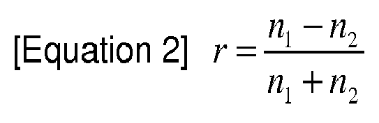
- By substituting the refractive index of each layer in the
Equation 2 to calculate the reflection coefficient at the interface, a pattern of the peaks which appear in the reflective wave can be estimated in advance. Referring to theEquation 2, according to thesample 3 of the embodiment, the refractive index of theYSZ layer 32 is approximately 6.0, the refractive index of theporous YSZ layer 31 is approximately 4.1, the refractive index of thecoating layer 33 is approximately 3.0, and the refractive index of the air is approximately 1.0. Thus, the reflection coefficients of the interfaces, C, D, E are assumed to be approximately -0.3, 0.2, and 0.6, respectively. -
Fig. 5 shows a schematic view of a pattern of the peaks (peak pattern) which is estimated from the reflection coefficients calculated from theEquation 2 using the pre-attained refractive index. According to theEquation 2, because the reflection coefficient is assumed to have negative value at the incident interface where the terahertz wave enters thesample 3 from the air, the indication of the positive and negative of the pattern of the peaks are defined to be opposite to the positive and negative of the reflection coefficient for the explanatory purpose. According to thesample 3 of the embodiment, the peak pattern in which the positive peak, negative peak, and negative peak appear in the mentioned order in the time waveform is estimated. Alternatively, the peak pattern may be determined on the basis of the actually measured value. - Further, in a case where a range of the layer thickness at the sample 3 (layer thickness range) is attained in advance, a temporal range, or time range between the peaks which appear in the waveform can be estimated. According to the embodiment, as explained hereinafter, by pre-determining the peak pattern and inputting the estimated value of the layer thickness range and an intensity ratio range, the peak corresponding to the interface can be accurately detected among the numerous peaks which appear in the waveform.
-
Fig. 6 shows a flowchart for the method for measuring layer thickness of the multilayer ceramic according to the embodiment. First, an operator sets thesample 3 including the multilayer ceramic which serves as an object of the inspection to the optical system 2 (Step S1). In this step, an angle of thesample 3 relative to theoptical system 2 is adjusted so that the terahertz wave reflected on thesample 3 passes through theaperture 19. Thereafter, upon the operation of thecontrol device 5 by the operator to activate a measurement program, theCPU 502 executes the measurement program stored in thememory device 504 to initialize theoptical system 2, the lock-inamplifier 4, and the control device 5 (Step S2). - Thereafter, the
control device 5 executes the measurement of the time waveform of the terahertz wave (Step S3). The optical pulse, or light pulse of thefemtosecond fiber laser 10 is split into the fundamental wave corresponding to 1550nm component and the second harmonic corresponding to 780nm component at thedichroic mirror 11, the fundamental wave is incident on, or enters thechopper 12, and the second harmonic is incident on, or enters theoptical delay portion 25. Thechopper 12 modulates the fundamental wave at a predetermined modulation frequency (e.g., 1 kHz). The modulated fundamental wave is reflected on themirror 13 and the fundamental wave collectingparabolic mirror 14, and is condensed at theDAST 15. The terahertz wave generated by theDAST 15 is reflected on the off-axis parabolic mirrors 16, 17 and is condensed, or collected at thesample 3. - The terahertz wave reflected on the
sample 3 is collimated by the off-axisparabolic mirror 18. Further, the terahertz wave passes through an opening portion of theaperture 19. According to the embodiment, by providing theaperture 19, the reflective wave at a periphery portion of the terahertz wave is blocked and the reflective wave at a center portion of the terahertz wave (regular reflection wave) only is allowed to pass through theaperture 19. According to the foregoing construction, the regular reflection wave of the terahertz wave which is reflected on thesample 3 only passes through the opening portion of theaperture 19 to be detected by theterahertz wave detector 22. - The terahertz wave which passed through the
aperture 19 is condensed, or collected at the gap of the dipole antenna provided at theterahertz wave detector 22 by means of the off-axisparabolic mirror 20. The pulse of the terahertz wave is repeatedly condensed, or collected at theterahertz wave detector 22 at the modulation frequency (1 kHz). On the other hand, the probe light which delays a predetermined time by means of theoptical delay portion 25 is irradiated at the gap of the dipole antenna provided at theterahertz wave detector 22. In those circumstances, a feeble electric current which is proportional to the electric field of the terahertz wave flows and the feeble electric current is synchronously detected by the lock-inamplifier 4. The lock-inamplifier 4 converts the amplified electric current to the digital data by means of an analog-to-digital converter (A/D converter) and stores the data in the memory. Thus, the intensity at the predetermined timing of the waveform of the terahertz wave is measured. - In order to sample the waveform of the terahertz wave, the electric field intensity at the
terahertz wave detector 22 is measured while shifting, or changing timing of the probe light. That is, thecontrol device 5 actuates the movable mirror of theoptical delay portion 25 to set a delay of the probe light at a delay time t1. The probe light is condensed at theterahertz wave detector 22, and the electric filed intensity of the terahertz wave at the timing of the delay time t1 is measured. Subsequently, thecontrol device 5 sets a delay time, or delay at theoptical delay portion 25 at a delay time t2. The electric field intensity of the terahertz wave at the timing of the delay time t2 is detected by theterahertz wave detector 22. Similarly, the delay at theoptical delay portion 25 is shifted to a delay time t3, delay time t4, and delay time t5, for example, in the mentioned order, and thus the time waveform of the terahertz wave is sampled. Thecontrol device 5 imports the measured data which shows the waveform of the terahertz wave to store the measured data in the memory device 504 (Step S4). - The
control device 5 extracts the peaks from the measured data and measures the layer thickness on the basis of the peaks (Step S5). The obtained measurement results are displayed on a display device provided at thecontrol device 5. After executing the foregoing processes, in a case where the measurement is continuously performed (i.e., NO at Step S6), thecontrol device 5 repeatedly executes the processes of Steps S3 to S5. On the other hand, in a case where the measurement is completed (i.e., YES at Step S6), thecontrol device 5 ends the processes, or transactions. -
Fig. 7 shows a flowchart explaining details of a layer thickness measurement process (Step S5) according to the embodiment. First, the operator inputs the information of layer structure (e.g., the number of layers, refraction index of each layer, refraction index of the air) included in the sample 3 (i.e., specifying types of layers)(Step S51). The refraction index of the air may be stored in thememory device 504 in advance. Alternatively, thecontrol device 5 displays the pre-recorded layer structures on the display device so as to allow the operator to select a layer structure. Thecontrol device 5 determines the peak pattern using theEquation 2 on the basis of the inputted layer structure to display the peak pattern on the display device (Step S52). That is, thecontrol device 5 substitutes the refractive index of each of the layers and the refractive index of the air that the operator inputted at Step S51 in theEquation 2 to calculate the reflection coefficient r of interfaces, and determines the peak pattern on the basis of the calculated reflection coefficient r relative to each of the interfaces, or boundaries. - Further, the operator inputs the intensity ratio range and the layer thickness range that each of the layers may have via an input device of the control device 5 (i.e., specifying layer thickness range and intensity ratio range)(Step S53). The layer thickness range is a range of values that the layer thickness may have (i.e., the minimum value and maximum value). The intensity ratio range is a range of values that a ratio of the intensity at a peak relative to the intensity at another peak may take (i.e., minimum value and maximum value). Alternatively, the intensity ratio may be determined on the basis of a ratio of the reflection coefficients between layers calculated by the
Equation 2. Further, alternatively, an intensity ratio range based on the actually measured values may be inputted. In a case where the observed peak or the layer thickness calculated based on the observed peak do not match the inputted intensity ratio range and the layer thickness range, it is determined that the observed peak is not caused by the reflection of the terahertz wave on the interface, or boundary (e.g., noise, multipath reflection, or multi reflection), and the observed peak is excluded. - The
control device 5 removes the noise using a frequency filter, for example, a low-pass filter, from the measured waveform data (i.e., applying frequency filter)(Step S54). Thereafter, thecontrol device 5 further removes noise components using a deconvolution filter which removes the noise components only (i.e., applying deconvolution filter)(Step S55). Regarding Step S54 and Step S55, alternatively, any filtering process may be performed as long as the noise is removable from the waveform data. Further, alternatively, in a case where the peak for calculating the layer thickness is detectable without removing the noise, the noise removing process may be omitted. - After attaining signal components only of the waveform data by the filtering process, the
control device 5 detects the peak from the waveform data (i.e., peak detection)(Step S56). Thereafter, thecontrol device 5 substitutes the time difference, or differential time between the detected peaks in theEquation 1 to calculate the layer thickness (i.e., calculating layer thickness)(Step S57). When the calculation of the layer thickness is completed, the transaction returns to the main flowchart illustrated inFig. 7 . -
Figs. 8A and8B show a flowchart explaining details of a peak detection processing (Step S56) according to the embodiment.Figs. 8A and8B show an example, and a flow of the peak detection processing varies depending on a peak pattern (i.e., the number of peaks and whether the peaks are positive or negative) of a sample which is an object to be measured. Thus, it is necessary to modify the peak detection processing in accordance with the peak pattern of the sample of the object to be measured. It is favorable that the peak detection processing corresponding to each peak pattern is predefined, and the peak detection processing is selected in accordance with the peak pattern determined at Step S52.Figs. 8A and8B show a flowchart for a case where the layer structure shown inFig. 4 is inputted at Step S51 and the peak pattern is determined as illustrated inFig. 5 at Step S52. - The
control device 5 scans the waveform data which is processed with the filtering at Step S54 and Step S55 (Step S101). Thecontrol device 5 detects the positive peak where the absolute value of the intensity is the maximum from the measurement data (i.e., waveform data) showing the time waveform of the terahertz wave scanned at Step S101 on the basis of the peak pattern determined at Step S52, and obtains time x1 corresponding to the peak (Step S102). The peak in this case is for the interface C between thecoating layer 33 and theYSZ layer 32. - Similarly, the
control device 5 detects the negative peak where the absolute value of the intensity is the maximum, and obtains time x3 corresponding to the peak (Step S103). The peak in this case is for the interface E between theporous YSZ layer 31 and the air. - Then, it is determined whether the layer thickness obtained from a difference of the time x1 and the time x3 on the basis of the Equation 1 (i.e., layer thickness of the lamination of the
YSZ layer 32 and the porous YSZ layer 31) is within a predetermined layer thickness range (Step S104). The layer thickness range is the range inputted at Step S53, and corresponds to the range defined by the minimum value and the maximum value that the layer thickness can have. - In a case where the layer thickness obtained from the difference of the time x1 and the time x3 does not fall within the predetermined layer thickness range (i.e., NO at Step S104), there is a possibility that the peak is not detected properly. Thus, until fulfilling the condition defined at Step S104, the transaction is repeated deeming, or assuming that the negative peak where the absolute value of the intensity is next to the maximum corresponds to the interface E of the
porous YSZ layer 31 and the air (Step S105). - Next, the
control device 5 detects the peak where the absolute value of the intensity is the maximum among the negative peaks existing from time x1 to time x3 to obtain time x2 of the detected peak (Step S106). The peak in this case is for the interface D of theYSZ layer 32 and theporous YSZ layer 31. Further, thecontrol device 5 determines whether the layer thickness obtained from the difference of time x3 and time x2 (i.e., the layer thickness of the porous YSZ layer 31) and the layer thickness obtained from the difference of time x2 and time x1 (i.e., the layer thickness of the YSZ layer 32) are within the predetermined layer thickness ranges (Step S107). The layer thickness ranges are inputted at Step S53 and correspond to the range defined by the minimum values and the maximum values that each of the layer thicknesses of theporous YSZ layer 31 and theYSZ layer 32 can have. - In a case where the layer thicknesses do not fall within the predetermined layer thickness ranges (i.e., NO at Step S107), it is possible that the peak is not properly detected. Thus, until fulfilling the conditions defined in Step S107, the transactions are repeated deeming, or assuming that the negative peak where the absolute value of the intensity is next to the maximum corresponds to the interface D of the
YSZ layer 32 and the porous YSZ layer 31 (Step S108). - Subsequently, the
control device 5 extracts peak values f(x1), f(x2), f(x3) of times x1, x2, x3, respectively, from the waveform data and determines whether each of intensity ratios f(x1)/f(x3), f(x2)/f(x3) of the peak values falls within the predetermined intensity ratio range (Step S109). Here, f(x) shows the intensity at time x. In those circumstances, although f(x3) is applied as a reference for the intensity ratio, in the embodiment, other definitions of the intensity ratio applying f(x1) or f(x2) as a reference are applicable. The intensity ratio range here is inputted at Step S53. - In a case where the conditions at Step S109 are satisfied, the
control device 5 outputs time x1, time x2, and time x3 as times, or timing for peaks corresponding to the interfaces, respectively (Step S110). In a case where the conditions at Step S109 are not satisfied, it is possible that the measurement error occurs. Thus, thecontrol device 5 outputs the time x1, time x2, and time x3 as times, or timing for peaks corresponding to the respective interfaces together with warning messages (Step S111). - As explained above, according to the construction of the embodiment, by detecting the plural peaks from the waveform data in accordance with the peak pattern determined by the
control device 5, an erroneous detection of multipath reflection, or multi reflection and noise as the peak of the interface is avoidable. Further, by detecting the peaks in a descending order from the peak having greater amplitude, or oscillation in the waveform data, an erroneous detection of multipath reflection, or multi reflection and noise as the peak of the interface is avoidable. Further, by pre-inputting the layer thickness range and the intensity ratio range of the sample which is the object of the measurement, a measurement error caused by an erroneous detection of the peak is avoidable. - According to the embodiment, the
control device 5 performs peak detection. Alternatively, the operator may determine the peak for calculating the layer thickness on the basis of the waveform data displayed on the display of thecontrol device 5 to specify the peak by the input device of thecontrol device 5. - Measurement of the layer thickness of a sample including multilayer ceramic using the method for measuring layer thickness according to the embodiment will be explained as follows.
Fig. 9 shows the waveform data of the terahertz wave obtained according to the embodiment. Horizontal axis inFig. 9 shows time (delay of pulse, delay (ps)) and vertical axis inFig. 9 shows the intensity. Thesample 3 which is applied as the object of the measurement includes the structure shown inFig. 4 . The layer thickness of thecoating layer 33 is 60µm, the layer thickness of theYSZ layer 32 is 20µm, and the layer thickness of theporous YSZ layer 31 is 400µm. - As illustrated in
Fig. 9 , in the peak detection processing (Step S56), it is detected that the positive peak at time x1 corresponds to the interface C shown inFig. 4 , the negative peak at time x2 corresponds to the interface D shown inFig. 4 , and the negative peak at time x3 corresponds to the interface E shown inFig. 4 . In those circumstances, the peak detection processing is performed disregarding the significant positive peak indicated with "y" because the peak indicated with "y" corresponds to the interface of the air and thecoating layer 33. Other peaks are presumed as caused by noises and multipath reflection, or multi reflection generated within the layer. According to thesample 3 of the embodiment, the terahertz wave is significantly attenuated, or decayed because theporous YSZ layer 31 is thick, and the peak at the time x3 is significantly small compared to the peak pattern estimated from the refractive index (seeFig. 5 ). -
Fig. 10 shows a measurement result of the layer thickness calculated from theEquation 1 on the basis of the waveform shown inFig. 9 . The delay of theYSZ layer 32 corresponds to the time difference, or differential time of the time x1 and the time x2 between the peaks, and the delay of theporous YSZ layer 31 corresponds to the time difference, or differential time of the time x2 and time x3 between the peaks. The estimated layer thicknesses (i.e., 17.5µm at theYSZ layer 32, 401µm at the porous YSZ layer 31) calculated on the basis of the delays are approximate to the values of actual layer thicknesses (i.e., 20µm at theYSZ layer 32, 400µm at the porous YSZ layer 31). According to the embodiment, the incidence angle of the terahertz wave to thesample 3 is approximately 10 degrees, which is deemed as small, and because the terahertz wave enters, or is incident on thesample 3 from the air to thesample 3 which includes large refractive index, the advancing angle of the terahertz wave in thesample 3 is assumed to be further smaller. Thus, according to the embodiment, cosθ in theEquation 1 is calculated to be approximate to one (1). In a case where it is necessary to obtain the result with higher precision, alternatively, the accurate cosθ may be calculated. - Thus, according to the method for measuring layer thickness of the embodiment, the layer thickness of each layer of the multilayer ceramic made from the same material and having different porosities can be measured.
A method for measuring a layer thickness includes a process for generating a terahertz wave, a process for irradiating the terahertz wave to a multilayer ceramic (3) having a plurality of ceramic layers, a process for obtaining a time waveform of the terahertz wave reflected on the multilayer ceramic (3), and a process for measuring a layer thickness of the ceramic layer on the basis of the time waveform.
Claims (4)
- A method for measuring a layer thickness, comprising
a process for generating a terahertz wave;
a process for irradiating the terahertz wave to a multilayer ceramic (3) having a plurality of ceramic layers;
a process for obtaining a time waveform of the terahertz wave reflected on the multilayer ceramic (3); and
a process for measuring a layer thickness of the ceramic layer on the basis of the time waveform. - The method for measuring the layer thickness according to claim 1, wherein
the multilayer ceramic (3) includes a first ceramic layer (31), and a second ceramic layer (32) which is in contact with the first ceramic layer (31) and includes a porosity different from a porosity of the first ceramic layer (31). - The method for measuring the layer thickness according to claim 2, wherein the first ceramic layer (31) and the second ceramic layer (32) are formed using a same ceramic material.
- The method for measuring the layer thickness according to claim 1, wherein the process for measuring the layer thickness includes a process for detecting two peaks corresponding to interfaces of the ceramic layers in the time waveform and a process for calculating the layer thickness on the basis of a time difference between said two peaks.
Applications Claiming Priority (1)
| Application Number | Priority Date | Filing Date | Title |
|---|---|---|---|
| JP2012229430A JP2014081285A (en) | 2012-10-17 | 2012-10-17 | Method of measuring film thickness of multilayer ceramic |
Publications (1)
| Publication Number | Publication Date |
|---|---|
| EP2722639A1 true EP2722639A1 (en) | 2014-04-23 |
Family
ID=49328420
Family Applications (1)
| Application Number | Title | Priority Date | Filing Date |
|---|---|---|---|
| EP13188420.7A Withdrawn EP2722639A1 (en) | 2012-10-17 | 2013-10-14 | Method for measuring layer thickness of multilayer ceramic |
Country Status (3)
| Country | Link |
|---|---|
| EP (1) | EP2722639A1 (en) |
| JP (1) | JP2014081285A (en) |
| CN (1) | CN103776382A (en) |
Cited By (8)
| Publication number | Priority date | Publication date | Assignee | Title |
|---|---|---|---|---|
| US20150176974A1 (en) * | 2013-12-20 | 2015-06-25 | Tokyo Electron Limited | Apparatus and method for measuring thickness and temperature and substrate processing system |
| EP2982932A1 (en) * | 2015-03-12 | 2016-02-10 | Proton Products International Limited | Measurement of industrial products manufactured by extrusion techniques using terahertz radiation |
| WO2017173533A1 (en) * | 2016-04-04 | 2017-10-12 | Tetechs Inc. | Methods and systems for thickness measurement of multi-layer structures |
| US20200209137A1 (en) * | 2018-12-31 | 2020-07-02 | Robert Bosch Gmbh | Mold detecting device using electromagnetic waves |
| US11060859B2 (en) | 2016-04-04 | 2021-07-13 | Tetechs Inc. | Methods and systems for thickness measurement of multi-layer structures |
| CN115507759A (en) * | 2022-07-22 | 2022-12-23 | 中国矿业大学 | Terahertz Measurement Method of Ceramic Layer Thickness Based on Adaptive Transfer Learning |
| US20230175960A1 (en) * | 2020-05-15 | 2023-06-08 | Helmut Fischer Gmbh Institut Fuer Elektronik Und Messtechnik | Apparatus for transmitting and/or receiving terahertz radiation, and control device therefor |
| US11726022B2 (en) | 2018-12-31 | 2023-08-15 | Robert Bosch Gmbh | Device for detecting mold |
Families Citing this family (13)
| Publication number | Priority date | Publication date | Assignee | Title |
|---|---|---|---|---|
| EP3265748B1 (en) * | 2015-03-03 | 2020-07-15 | Sikora Ag | Device and method for measuring the wall thickness of a tube |
| JP6589239B2 (en) * | 2015-09-25 | 2019-10-16 | 株式会社Screenホールディングス | Film thickness measuring apparatus and film thickness measuring method |
| KR101818416B1 (en) * | 2016-06-13 | 2018-01-16 | 한국전력공사 | Measurement method for porous combustion coating thickness |
| CN106370109A (en) * | 2016-08-19 | 2017-02-01 | 南开大学 | Bridge foundation pile steel reinforcement cage length detection apparatus and detection method |
| NL2020921A (en) * | 2017-06-07 | 2018-12-13 | Stichting Vu | Alignment Measurement System |
| CN107356599B (en) * | 2017-06-23 | 2020-02-18 | 厦门大学 | A terahertz nondestructive testing method for ceramic matrix composites |
| CN108332674B (en) * | 2018-02-11 | 2020-01-21 | 中国科学院电子学研究所 | Method for calculating thickness and porosity of porous film by single spectrum |
| CN108592805A (en) * | 2018-04-11 | 2018-09-28 | 青岛万龙智控科技有限公司 | The reflective On-line Measuring Method of THz wave of multifilm thickness |
| CN108535212A (en) * | 2018-04-11 | 2018-09-14 | 华东理工大学 | A kind of test method of the erosion pattern of the thermal barrier coating based on Terahertz Technology |
| KR102075356B1 (en) * | 2018-08-27 | 2020-02-10 | 한양대학교 산학협력단 | Specimen thickness measuring device and Specimen Thickness Measuring Method |
| CN109581133B (en) * | 2019-01-24 | 2020-10-09 | 黄河科技学院 | Performance testing device based on antiferroelectric material |
| CN110243296A (en) * | 2019-06-21 | 2019-09-17 | 上海理工大学 | Device and method for non-destructive measurement of pearl layer thickness |
| KR102167799B1 (en) * | 2019-07-24 | 2020-10-20 | 한양대학교 산학협력단 | Thickness measuring device |
Citations (7)
| Publication number | Priority date | Publication date | Assignee | Title |
|---|---|---|---|---|
| JP2004028618A (en) * | 2002-06-21 | 2004-01-29 | Osaka Industrial Promotion Organization | Paint film measurement method and device |
| JP2004333366A (en) | 2003-05-09 | 2004-11-25 | Toshiba Ceramics Co Ltd | Ceramics film thickness measurement method by ultrasonic diffraction method |
| US6828558B1 (en) * | 1999-06-04 | 2004-12-07 | Teraview Limited | Three dimensional imaging |
| WO2005052509A1 (en) * | 2003-11-25 | 2005-06-09 | Canon Kabushiki Kaisha | System and method for counting the number of layers of a multilayer object by means of electromagnetic waves |
| EP2196766A1 (en) * | 2008-12-12 | 2010-06-16 | Aisin Seiki Kabushiki Kaisha | Device and method for measuring thickness of paint film in non-contacting manner |
| US7876423B1 (en) * | 2008-06-27 | 2011-01-25 | The United States Of America As Represented By The National Aeronautics And Space Administration | Simultaneous noncontact precision imaging of microstructural and thickness variation in dielectric materials using terahertz energy |
| WO2011105040A1 (en) * | 2010-02-26 | 2011-09-01 | アイシン精機株式会社 | Coating film inspection apparatus and inspection method |
Family Cites Families (7)
| Publication number | Priority date | Publication date | Assignee | Title |
|---|---|---|---|---|
| JP4383062B2 (en) * | 2003-01-31 | 2009-12-16 | コバレントマテリアル株式会社 | Method for producing porous silicon carbide sintered body |
| JP2005043230A (en) * | 2003-07-23 | 2005-02-17 | Institute Of Physical & Chemical Research | Elongated member defect detection method and apparatus |
| JP5371293B2 (en) * | 2007-08-31 | 2013-12-18 | キヤノン株式会社 | Apparatus and method for obtaining information about terahertz waves |
| EP2202481A1 (en) * | 2007-10-16 | 2010-06-30 | Aisin Seiki Kabushiki Kaisha | Non-contact film thickness measurement method and device |
| JP5353121B2 (en) * | 2008-08-26 | 2013-11-27 | アイシン精機株式会社 | Terahertz wave generation apparatus and terahertz wave generation method |
| JP2010156544A (en) * | 2008-12-26 | 2010-07-15 | Aisin Seiki Co Ltd | Terahertz light measuring device |
| CN102620666A (en) * | 2012-03-29 | 2012-08-01 | 吴周令 | Detecting system for semiconductor wafer thickness and detecting method thereof |
-
2012
- 2012-10-17 JP JP2012229430A patent/JP2014081285A/en active Pending
-
2013
- 2013-09-29 CN CN201310455351.7A patent/CN103776382A/en active Pending
- 2013-10-14 EP EP13188420.7A patent/EP2722639A1/en not_active Withdrawn
Patent Citations (7)
| Publication number | Priority date | Publication date | Assignee | Title |
|---|---|---|---|---|
| US6828558B1 (en) * | 1999-06-04 | 2004-12-07 | Teraview Limited | Three dimensional imaging |
| JP2004028618A (en) * | 2002-06-21 | 2004-01-29 | Osaka Industrial Promotion Organization | Paint film measurement method and device |
| JP2004333366A (en) | 2003-05-09 | 2004-11-25 | Toshiba Ceramics Co Ltd | Ceramics film thickness measurement method by ultrasonic diffraction method |
| WO2005052509A1 (en) * | 2003-11-25 | 2005-06-09 | Canon Kabushiki Kaisha | System and method for counting the number of layers of a multilayer object by means of electromagnetic waves |
| US7876423B1 (en) * | 2008-06-27 | 2011-01-25 | The United States Of America As Represented By The National Aeronautics And Space Administration | Simultaneous noncontact precision imaging of microstructural and thickness variation in dielectric materials using terahertz energy |
| EP2196766A1 (en) * | 2008-12-12 | 2010-06-16 | Aisin Seiki Kabushiki Kaisha | Device and method for measuring thickness of paint film in non-contacting manner |
| WO2011105040A1 (en) * | 2010-02-26 | 2011-09-01 | アイシン精機株式会社 | Coating film inspection apparatus and inspection method |
Cited By (12)
| Publication number | Priority date | Publication date | Assignee | Title |
|---|---|---|---|---|
| US20150176974A1 (en) * | 2013-12-20 | 2015-06-25 | Tokyo Electron Limited | Apparatus and method for measuring thickness and temperature and substrate processing system |
| US9163931B2 (en) * | 2013-12-20 | 2015-10-20 | Tokyo Electron Limited | Apparatus and method for measuring thickness and temperature and substrate processing system |
| EP2982932A1 (en) * | 2015-03-12 | 2016-02-10 | Proton Products International Limited | Measurement of industrial products manufactured by extrusion techniques using terahertz radiation |
| WO2017173533A1 (en) * | 2016-04-04 | 2017-10-12 | Tetechs Inc. | Methods and systems for thickness measurement of multi-layer structures |
| US20190078873A1 (en) * | 2016-04-04 | 2019-03-14 | Tetechs Inc. | Methods and systems for thickness measurement of multi-layer structures |
| US11060859B2 (en) | 2016-04-04 | 2021-07-13 | Tetechs Inc. | Methods and systems for thickness measurement of multi-layer structures |
| US20200209137A1 (en) * | 2018-12-31 | 2020-07-02 | Robert Bosch Gmbh | Mold detecting device using electromagnetic waves |
| US11726022B2 (en) | 2018-12-31 | 2023-08-15 | Robert Bosch Gmbh | Device for detecting mold |
| US11867603B2 (en) * | 2018-12-31 | 2024-01-09 | Robert Bosch Gmbh | Mold detecting device using electromagnetic waves |
| US20230175960A1 (en) * | 2020-05-15 | 2023-06-08 | Helmut Fischer Gmbh Institut Fuer Elektronik Und Messtechnik | Apparatus for transmitting and/or receiving terahertz radiation, and control device therefor |
| US12571729B2 (en) * | 2020-05-15 | 2026-03-10 | Helmut Fischer Gmbh Institut Fuer Elektronik Und Messtechnik | Apparatus for transmitting and/or receiving terahertz radiation, and control device therefor |
| CN115507759A (en) * | 2022-07-22 | 2022-12-23 | 中国矿业大学 | Terahertz Measurement Method of Ceramic Layer Thickness Based on Adaptive Transfer Learning |
Also Published As
| Publication number | Publication date |
|---|---|
| JP2014081285A (en) | 2014-05-08 |
| CN103776382A (en) | 2014-05-07 |
Similar Documents
| Publication | Publication Date | Title |
|---|---|---|
| JP2014081285A (en) | Method of measuring film thickness of multilayer ceramic | |
| CN102770750B (en) | Coating film inspection apparatus and inspection method | |
| CN103348235B (en) | Device for detecting foreign matter and method for detecting foreign matter | |
| JP6096725B2 (en) | Film thickness measuring apparatus and film thickness measuring method | |
| US20100195090A1 (en) | Device for measuring thickness of paint film in non-contacting manner | |
| US10578555B2 (en) | Acoustic resonance spectrometry system and method | |
| CN110927121B (en) | Phase type SPR detection device and method based on white light interference spectrum | |
| JP6238058B2 (en) | Terahertz spectroscopy system | |
| US7755752B1 (en) | Combined modulated optical reflectance and photoreflectance system | |
| US7798000B1 (en) | Non-destructive imaging, characterization or measurement of thin items using laser-generated lamb waves | |
| JP2011127950A (en) | Liquid thin-film forming device | |
| US8450689B2 (en) | Device and method for measuring thickness of paint film in non-contacting manner | |
| CN103884683B (en) | Based on the optical sensor of F-P semiconductor laser and the cascade of film F-P optical filter | |
| JP5618119B2 (en) | Terahertz light detection element and optical equipment | |
| US6952261B2 (en) | System for performing ellipsometry using an auxiliary pump beam to reduce effective measurement spot size | |
| US10809189B2 (en) | Optical measurement device and optical measurement method | |
| CN102445328B (en) | Method for realizing absolute measurement of absorption loss of optical thin film element | |
| JP4474795B2 (en) | Film thickness measuring method, measuring apparatus and semiconductor device manufacturing method | |
| WO2015163298A1 (en) | Electromagnetic-wave measurement device, measurement method, program and recording medium | |
| Benis et al. | Nondegenerate, transient nonlinear refraction of indium tin oxide excited at epsilon-near-zero | |
| JP2012141473A (en) | Etalon filter, frequency calibration system using etalon filter, and frequency calibration method | |
| US10247659B2 (en) | Device for characterizing an interface of a structure and corresponding device | |
| JP2002181700A (en) | Surface plasmon resonance measuring apparatus | |
| JP2019023593A (en) | Laser displacement meter and laser ultrasonic inspection device using the same | |
| CN121276264A (en) | Partial discharge detection system based on Redberg atomic quantum coherence effect |
Legal Events
| Date | Code | Title | Description |
|---|---|---|---|
| PUAI | Public reference made under article 153(3) epc to a published international application that has entered the european phase |
Free format text: ORIGINAL CODE: 0009012 |
|
| AK | Designated contracting states |
Kind code of ref document: A1 Designated state(s): AL AT BE BG CH CY CZ DE DK EE ES FI FR GB GR HR HU IE IS IT LI LT LU LV MC MK MT NL NO PL PT RO RS SE SI SK SM TR |
|
| AX | Request for extension of the european patent |
Extension state: BA ME |
|
| 17P | Request for examination filed |
Effective date: 20140506 |
|
| RBV | Designated contracting states (corrected) |
Designated state(s): AL AT BE BG CH CY CZ DE DK EE ES FI FR GB GR HR HU IE IS IT LI LT LU LV MC MK MT NL NO PL PT RO RS SE SI SK SM TR |
|
| STAA | Information on the status of an ep patent application or granted ep patent |
Free format text: STATUS: THE APPLICATION HAS BEEN WITHDRAWN |
|
| 18W | Application withdrawn |
Effective date: 20160629 |